EP3637181B1 - Elektrodenkonfiguration für eine flüssigkristallanzeige - Google Patents
Elektrodenkonfiguration für eine flüssigkristallanzeige Download PDFInfo
- Publication number
- EP3637181B1 EP3637181B1 EP19202593.0A EP19202593A EP3637181B1 EP 3637181 B1 EP3637181 B1 EP 3637181B1 EP 19202593 A EP19202593 A EP 19202593A EP 3637181 B1 EP3637181 B1 EP 3637181B1
- Authority
- EP
- European Patent Office
- Prior art keywords
- slit
- electrode
- data line
- pixel
- pixel electrode
- Prior art date
- Legal status (The legal status is an assumption and is not a legal conclusion. Google has not performed a legal analysis and makes no representation as to the accuracy of the status listed.)
- Active
Links
Images






Classifications
-
- G—PHYSICS
- G02—OPTICS
- G02F—OPTICAL DEVICES OR ARRANGEMENTS FOR THE CONTROL OF LIGHT BY MODIFICATION OF THE OPTICAL PROPERTIES OF THE MEDIA OF THE ELEMENTS INVOLVED THEREIN; NON-LINEAR OPTICS; FREQUENCY-CHANGING OF LIGHT; OPTICAL LOGIC ELEMENTS; OPTICAL ANALOGUE/DIGITAL CONVERTERS
- G02F1/00—Devices or arrangements for the control of the intensity, colour, phase, polarisation or direction of light arriving from an independent light source, e.g. switching, gating or modulating; Non-linear optics
- G02F1/01—Devices or arrangements for the control of the intensity, colour, phase, polarisation or direction of light arriving from an independent light source, e.g. switching, gating or modulating; Non-linear optics for the control of the intensity, phase, polarisation or colour
- G02F1/13—Devices or arrangements for the control of the intensity, colour, phase, polarisation or direction of light arriving from an independent light source, e.g. switching, gating or modulating; Non-linear optics for the control of the intensity, phase, polarisation or colour based on liquid crystals, e.g. single liquid crystal display cells
- G02F1/133—Constructional arrangements; Operation of liquid crystal cells; Circuit arrangements
- G02F1/1333—Constructional arrangements; Manufacturing methods
- G02F1/1337—Surface-induced orientation of the liquid crystal molecules, e.g. by alignment layers
- G02F1/133707—Structures for producing distorted electric fields, e.g. bumps, protrusions, recesses, slits in pixel electrodes
-
- G—PHYSICS
- G02—OPTICS
- G02F—OPTICAL DEVICES OR ARRANGEMENTS FOR THE CONTROL OF LIGHT BY MODIFICATION OF THE OPTICAL PROPERTIES OF THE MEDIA OF THE ELEMENTS INVOLVED THEREIN; NON-LINEAR OPTICS; FREQUENCY-CHANGING OF LIGHT; OPTICAL LOGIC ELEMENTS; OPTICAL ANALOGUE/DIGITAL CONVERTERS
- G02F1/00—Devices or arrangements for the control of the intensity, colour, phase, polarisation or direction of light arriving from an independent light source, e.g. switching, gating or modulating; Non-linear optics
- G02F1/01—Devices or arrangements for the control of the intensity, colour, phase, polarisation or direction of light arriving from an independent light source, e.g. switching, gating or modulating; Non-linear optics for the control of the intensity, phase, polarisation or colour
- G02F1/13—Devices or arrangements for the control of the intensity, colour, phase, polarisation or direction of light arriving from an independent light source, e.g. switching, gating or modulating; Non-linear optics for the control of the intensity, phase, polarisation or colour based on liquid crystals, e.g. single liquid crystal display cells
- G02F1/133—Constructional arrangements; Operation of liquid crystal cells; Circuit arrangements
- G02F1/1333—Constructional arrangements; Manufacturing methods
- G02F1/1343—Electrodes
- G02F1/134309—Electrodes characterised by their geometrical arrangement
- G02F1/134363—Electrodes characterised by their geometrical arrangement for applying an electric field parallel to the substrate, i.e. in-plane switching [IPS]
-
- G—PHYSICS
- G02—OPTICS
- G02F—OPTICAL DEVICES OR ARRANGEMENTS FOR THE CONTROL OF LIGHT BY MODIFICATION OF THE OPTICAL PROPERTIES OF THE MEDIA OF THE ELEMENTS INVOLVED THEREIN; NON-LINEAR OPTICS; FREQUENCY-CHANGING OF LIGHT; OPTICAL LOGIC ELEMENTS; OPTICAL ANALOGUE/DIGITAL CONVERTERS
- G02F1/00—Devices or arrangements for the control of the intensity, colour, phase, polarisation or direction of light arriving from an independent light source, e.g. switching, gating or modulating; Non-linear optics
- G02F1/01—Devices or arrangements for the control of the intensity, colour, phase, polarisation or direction of light arriving from an independent light source, e.g. switching, gating or modulating; Non-linear optics for the control of the intensity, phase, polarisation or colour
- G02F1/13—Devices or arrangements for the control of the intensity, colour, phase, polarisation or direction of light arriving from an independent light source, e.g. switching, gating or modulating; Non-linear optics for the control of the intensity, phase, polarisation or colour based on liquid crystals, e.g. single liquid crystal display cells
- G02F1/133—Constructional arrangements; Operation of liquid crystal cells; Circuit arrangements
- G02F1/136—Liquid crystal cells structurally associated with a semi-conducting layer or substrate, e.g. cells forming part of an integrated circuit
- G02F1/1362—Active matrix addressed cells
- G02F1/136286—Wiring, e.g. gate line, drain line
-
- G—PHYSICS
- G02—OPTICS
- G02F—OPTICAL DEVICES OR ARRANGEMENTS FOR THE CONTROL OF LIGHT BY MODIFICATION OF THE OPTICAL PROPERTIES OF THE MEDIA OF THE ELEMENTS INVOLVED THEREIN; NON-LINEAR OPTICS; FREQUENCY-CHANGING OF LIGHT; OPTICAL LOGIC ELEMENTS; OPTICAL ANALOGUE/DIGITAL CONVERTERS
- G02F1/00—Devices or arrangements for the control of the intensity, colour, phase, polarisation or direction of light arriving from an independent light source, e.g. switching, gating or modulating; Non-linear optics
- G02F1/01—Devices or arrangements for the control of the intensity, colour, phase, polarisation or direction of light arriving from an independent light source, e.g. switching, gating or modulating; Non-linear optics for the control of the intensity, phase, polarisation or colour
- G02F1/13—Devices or arrangements for the control of the intensity, colour, phase, polarisation or direction of light arriving from an independent light source, e.g. switching, gating or modulating; Non-linear optics for the control of the intensity, phase, polarisation or colour based on liquid crystals, e.g. single liquid crystal display cells
- G02F1/133—Constructional arrangements; Operation of liquid crystal cells; Circuit arrangements
- G02F1/1333—Constructional arrangements; Manufacturing methods
- G02F1/133345—Insulating layers
-
- G—PHYSICS
- G02—OPTICS
- G02F—OPTICAL DEVICES OR ARRANGEMENTS FOR THE CONTROL OF LIGHT BY MODIFICATION OF THE OPTICAL PROPERTIES OF THE MEDIA OF THE ELEMENTS INVOLVED THEREIN; NON-LINEAR OPTICS; FREQUENCY-CHANGING OF LIGHT; OPTICAL LOGIC ELEMENTS; OPTICAL ANALOGUE/DIGITAL CONVERTERS
- G02F1/00—Devices or arrangements for the control of the intensity, colour, phase, polarisation or direction of light arriving from an independent light source, e.g. switching, gating or modulating; Non-linear optics
- G02F1/01—Devices or arrangements for the control of the intensity, colour, phase, polarisation or direction of light arriving from an independent light source, e.g. switching, gating or modulating; Non-linear optics for the control of the intensity, phase, polarisation or colour
- G02F1/13—Devices or arrangements for the control of the intensity, colour, phase, polarisation or direction of light arriving from an independent light source, e.g. switching, gating or modulating; Non-linear optics for the control of the intensity, phase, polarisation or colour based on liquid crystals, e.g. single liquid crystal display cells
- G02F1/133—Constructional arrangements; Operation of liquid crystal cells; Circuit arrangements
- G02F1/1333—Constructional arrangements; Manufacturing methods
- G02F1/1335—Structural association of cells with optical devices, e.g. polarisers or reflectors
- G02F1/133509—Filters, e.g. light shielding masks
- G02F1/133514—Colour filters
-
- G—PHYSICS
- G02—OPTICS
- G02F—OPTICAL DEVICES OR ARRANGEMENTS FOR THE CONTROL OF LIGHT BY MODIFICATION OF THE OPTICAL PROPERTIES OF THE MEDIA OF THE ELEMENTS INVOLVED THEREIN; NON-LINEAR OPTICS; FREQUENCY-CHANGING OF LIGHT; OPTICAL LOGIC ELEMENTS; OPTICAL ANALOGUE/DIGITAL CONVERTERS
- G02F1/00—Devices or arrangements for the control of the intensity, colour, phase, polarisation or direction of light arriving from an independent light source, e.g. switching, gating or modulating; Non-linear optics
- G02F1/01—Devices or arrangements for the control of the intensity, colour, phase, polarisation or direction of light arriving from an independent light source, e.g. switching, gating or modulating; Non-linear optics for the control of the intensity, phase, polarisation or colour
- G02F1/13—Devices or arrangements for the control of the intensity, colour, phase, polarisation or direction of light arriving from an independent light source, e.g. switching, gating or modulating; Non-linear optics for the control of the intensity, phase, polarisation or colour based on liquid crystals, e.g. single liquid crystal display cells
- G02F1/133—Constructional arrangements; Operation of liquid crystal cells; Circuit arrangements
- G02F1/1333—Constructional arrangements; Manufacturing methods
- G02F1/1343—Electrodes
-
- G—PHYSICS
- G02—OPTICS
- G02F—OPTICAL DEVICES OR ARRANGEMENTS FOR THE CONTROL OF LIGHT BY MODIFICATION OF THE OPTICAL PROPERTIES OF THE MEDIA OF THE ELEMENTS INVOLVED THEREIN; NON-LINEAR OPTICS; FREQUENCY-CHANGING OF LIGHT; OPTICAL LOGIC ELEMENTS; OPTICAL ANALOGUE/DIGITAL CONVERTERS
- G02F1/00—Devices or arrangements for the control of the intensity, colour, phase, polarisation or direction of light arriving from an independent light source, e.g. switching, gating or modulating; Non-linear optics
- G02F1/01—Devices or arrangements for the control of the intensity, colour, phase, polarisation or direction of light arriving from an independent light source, e.g. switching, gating or modulating; Non-linear optics for the control of the intensity, phase, polarisation or colour
- G02F1/13—Devices or arrangements for the control of the intensity, colour, phase, polarisation or direction of light arriving from an independent light source, e.g. switching, gating or modulating; Non-linear optics for the control of the intensity, phase, polarisation or colour based on liquid crystals, e.g. single liquid crystal display cells
- G02F1/133—Constructional arrangements; Operation of liquid crystal cells; Circuit arrangements
- G02F1/1333—Constructional arrangements; Manufacturing methods
- G02F1/1343—Electrodes
- G02F1/134309—Electrodes characterised by their geometrical arrangement
- G02F1/134336—Matrix
-
- G—PHYSICS
- G02—OPTICS
- G02F—OPTICAL DEVICES OR ARRANGEMENTS FOR THE CONTROL OF LIGHT BY MODIFICATION OF THE OPTICAL PROPERTIES OF THE MEDIA OF THE ELEMENTS INVOLVED THEREIN; NON-LINEAR OPTICS; FREQUENCY-CHANGING OF LIGHT; OPTICAL LOGIC ELEMENTS; OPTICAL ANALOGUE/DIGITAL CONVERTERS
- G02F1/00—Devices or arrangements for the control of the intensity, colour, phase, polarisation or direction of light arriving from an independent light source, e.g. switching, gating or modulating; Non-linear optics
- G02F1/01—Devices or arrangements for the control of the intensity, colour, phase, polarisation or direction of light arriving from an independent light source, e.g. switching, gating or modulating; Non-linear optics for the control of the intensity, phase, polarisation or colour
- G02F1/13—Devices or arrangements for the control of the intensity, colour, phase, polarisation or direction of light arriving from an independent light source, e.g. switching, gating or modulating; Non-linear optics for the control of the intensity, phase, polarisation or colour based on liquid crystals, e.g. single liquid crystal display cells
- G02F1/133—Constructional arrangements; Operation of liquid crystal cells; Circuit arrangements
- G02F1/136—Liquid crystal cells structurally associated with a semi-conducting layer or substrate, e.g. cells forming part of an integrated circuit
- G02F1/1362—Active matrix addressed cells
- G02F1/1368—Active matrix addressed cells in which the switching element is a three-electrode device
-
- G—PHYSICS
- G02—OPTICS
- G02F—OPTICAL DEVICES OR ARRANGEMENTS FOR THE CONTROL OF LIGHT BY MODIFICATION OF THE OPTICAL PROPERTIES OF THE MEDIA OF THE ELEMENTS INVOLVED THEREIN; NON-LINEAR OPTICS; FREQUENCY-CHANGING OF LIGHT; OPTICAL LOGIC ELEMENTS; OPTICAL ANALOGUE/DIGITAL CONVERTERS
- G02F1/00—Devices or arrangements for the control of the intensity, colour, phase, polarisation or direction of light arriving from an independent light source, e.g. switching, gating or modulating; Non-linear optics
- G02F1/01—Devices or arrangements for the control of the intensity, colour, phase, polarisation or direction of light arriving from an independent light source, e.g. switching, gating or modulating; Non-linear optics for the control of the intensity, phase, polarisation or colour
- G02F1/13—Devices or arrangements for the control of the intensity, colour, phase, polarisation or direction of light arriving from an independent light source, e.g. switching, gating or modulating; Non-linear optics for the control of the intensity, phase, polarisation or colour based on liquid crystals, e.g. single liquid crystal display cells
- G02F1/133—Constructional arrangements; Operation of liquid crystal cells; Circuit arrangements
- G02F1/136—Liquid crystal cells structurally associated with a semi-conducting layer or substrate, e.g. cells forming part of an integrated circuit
- G02F1/1362—Active matrix addressed cells
- G02F1/136218—Shield electrodes
-
- G—PHYSICS
- G02—OPTICS
- G02F—OPTICAL DEVICES OR ARRANGEMENTS FOR THE CONTROL OF LIGHT BY MODIFICATION OF THE OPTICAL PROPERTIES OF THE MEDIA OF THE ELEMENTS INVOLVED THEREIN; NON-LINEAR OPTICS; FREQUENCY-CHANGING OF LIGHT; OPTICAL LOGIC ELEMENTS; OPTICAL ANALOGUE/DIGITAL CONVERTERS
- G02F1/00—Devices or arrangements for the control of the intensity, colour, phase, polarisation or direction of light arriving from an independent light source, e.g. switching, gating or modulating; Non-linear optics
- G02F1/01—Devices or arrangements for the control of the intensity, colour, phase, polarisation or direction of light arriving from an independent light source, e.g. switching, gating or modulating; Non-linear optics for the control of the intensity, phase, polarisation or colour
- G02F1/13—Devices or arrangements for the control of the intensity, colour, phase, polarisation or direction of light arriving from an independent light source, e.g. switching, gating or modulating; Non-linear optics for the control of the intensity, phase, polarisation or colour based on liquid crystals, e.g. single liquid crystal display cells
- G02F1/133—Constructional arrangements; Operation of liquid crystal cells; Circuit arrangements
- G02F1/136—Liquid crystal cells structurally associated with a semi-conducting layer or substrate, e.g. cells forming part of an integrated circuit
- G02F1/1362—Active matrix addressed cells
- G02F1/136222—Colour filters incorporated in the active matrix substrate
-
- G—PHYSICS
- G02—OPTICS
- G02F—OPTICAL DEVICES OR ARRANGEMENTS FOR THE CONTROL OF LIGHT BY MODIFICATION OF THE OPTICAL PROPERTIES OF THE MEDIA OF THE ELEMENTS INVOLVED THEREIN; NON-LINEAR OPTICS; FREQUENCY-CHANGING OF LIGHT; OPTICAL LOGIC ELEMENTS; OPTICAL ANALOGUE/DIGITAL CONVERTERS
- G02F1/00—Devices or arrangements for the control of the intensity, colour, phase, polarisation or direction of light arriving from an independent light source, e.g. switching, gating or modulating; Non-linear optics
- G02F1/01—Devices or arrangements for the control of the intensity, colour, phase, polarisation or direction of light arriving from an independent light source, e.g. switching, gating or modulating; Non-linear optics for the control of the intensity, phase, polarisation or colour
- G02F1/13—Devices or arrangements for the control of the intensity, colour, phase, polarisation or direction of light arriving from an independent light source, e.g. switching, gating or modulating; Non-linear optics for the control of the intensity, phase, polarisation or colour based on liquid crystals, e.g. single liquid crystal display cells
- G02F1/137—Devices or arrangements for the control of the intensity, colour, phase, polarisation or direction of light arriving from an independent light source, e.g. switching, gating or modulating; Non-linear optics for the control of the intensity, phase, polarisation or colour based on liquid crystals, e.g. single liquid crystal display cells characterised by the electro-optical or magneto-optical effect, e.g. field-induced phase transition, orientation effect, guest-host interaction or dynamic scattering
- G02F1/139—Devices or arrangements for the control of the intensity, colour, phase, polarisation or direction of light arriving from an independent light source, e.g. switching, gating or modulating; Non-linear optics for the control of the intensity, phase, polarisation or colour based on liquid crystals, e.g. single liquid crystal display cells characterised by the electro-optical or magneto-optical effect, e.g. field-induced phase transition, orientation effect, guest-host interaction or dynamic scattering based on orientation effects in which the liquid crystal remains transparent
- G02F1/1393—Devices or arrangements for the control of the intensity, colour, phase, polarisation or direction of light arriving from an independent light source, e.g. switching, gating or modulating; Non-linear optics for the control of the intensity, phase, polarisation or colour based on liquid crystals, e.g. single liquid crystal display cells characterised by the electro-optical or magneto-optical effect, e.g. field-induced phase transition, orientation effect, guest-host interaction or dynamic scattering based on orientation effects in which the liquid crystal remains transparent the birefringence of the liquid crystal being electrically controlled, e.g. ECB-, DAP-, HAN-, PI-LC cells
-
- G—PHYSICS
- G02—OPTICS
- G02F—OPTICAL DEVICES OR ARRANGEMENTS FOR THE CONTROL OF LIGHT BY MODIFICATION OF THE OPTICAL PROPERTIES OF THE MEDIA OF THE ELEMENTS INVOLVED THEREIN; NON-LINEAR OPTICS; FREQUENCY-CHANGING OF LIGHT; OPTICAL LOGIC ELEMENTS; OPTICAL ANALOGUE/DIGITAL CONVERTERS
- G02F2201/00—Constructional arrangements not provided for in groups G02F1/00 - G02F7/00
- G02F2201/12—Constructional arrangements not provided for in groups G02F1/00 - G02F7/00 electrode
- G02F2201/123—Constructional arrangements not provided for in groups G02F1/00 - G02F7/00 electrode pixel
-
- G—PHYSICS
- G09—EDUCATION; CRYPTOGRAPHY; DISPLAY; ADVERTISING; SEALS
- G09G—ARRANGEMENTS OR CIRCUITS FOR CONTROL OF INDICATING DEVICES USING STATIC MEANS TO PRESENT VARIABLE INFORMATION
- G09G2300/00—Aspects of the constitution of display devices
- G09G2300/04—Structural and physical details of display devices
- G09G2300/0421—Structural details of the set of electrodes
- G09G2300/0426—Layout of electrodes and connections
-
- G—PHYSICS
- G09—EDUCATION; CRYPTOGRAPHY; DISPLAY; ADVERTISING; SEALS
- G09G—ARRANGEMENTS OR CIRCUITS FOR CONTROL OF INDICATING DEVICES USING STATIC MEANS TO PRESENT VARIABLE INFORMATION
- G09G2300/00—Aspects of the constitution of display devices
- G09G2300/04—Structural and physical details of display devices
- G09G2300/0439—Pixel structures
- G09G2300/0443—Pixel structures with several sub-pixels for the same colour in a pixel, not specifically used to display gradations
- G09G2300/0447—Pixel structures with several sub-pixels for the same colour in a pixel, not specifically used to display gradations for multi-domain technique to improve the viewing angle in a liquid crystal display, such as multi-vertical alignment [MVA]
-
- G—PHYSICS
- G09—EDUCATION; CRYPTOGRAPHY; DISPLAY; ADVERTISING; SEALS
- G09G—ARRANGEMENTS OR CIRCUITS FOR CONTROL OF INDICATING DEVICES USING STATIC MEANS TO PRESENT VARIABLE INFORMATION
- G09G2310/00—Command of the display device
- G09G2310/02—Addressing, scanning or driving the display screen or processing steps related thereto
- G09G2310/0202—Addressing of scan or signal lines
- G09G2310/0205—Simultaneous scanning of several lines in flat panels
-
- G—PHYSICS
- G09—EDUCATION; CRYPTOGRAPHY; DISPLAY; ADVERTISING; SEALS
- G09G—ARRANGEMENTS OR CIRCUITS FOR CONTROL OF INDICATING DEVICES USING STATIC MEANS TO PRESENT VARIABLE INFORMATION
- G09G3/00—Control arrangements or circuits, of interest only in connection with visual indicators other than cathode-ray tubes
- G09G3/20—Control arrangements or circuits, of interest only in connection with visual indicators other than cathode-ray tubes for presentation of an assembly of a number of characters, e.g. a page, by composing the assembly by combination of individual elements arranged in a matrix no fixed position being assigned to or needed to be assigned to the individual characters or partial characters
- G09G3/34—Control arrangements or circuits, of interest only in connection with visual indicators other than cathode-ray tubes for presentation of an assembly of a number of characters, e.g. a page, by composing the assembly by combination of individual elements arranged in a matrix no fixed position being assigned to or needed to be assigned to the individual characters or partial characters by control of light from an independent source
- G09G3/36—Control arrangements or circuits, of interest only in connection with visual indicators other than cathode-ray tubes for presentation of an assembly of a number of characters, e.g. a page, by composing the assembly by combination of individual elements arranged in a matrix no fixed position being assigned to or needed to be assigned to the individual characters or partial characters by control of light from an independent source using liquid crystals
- G09G3/3611—Control of matrices with row and column drivers
- G09G3/3614—Control of polarity reversal in general
Definitions
- Exemplary embodiments of the invention relate generally to a display device and, more specifically, to a liquid crystal display with improved display quality.
- Liquid crystal displays are widely used as a display device.
- a liquid crystal display includes two display panels and a liquid crystal layer disposed between field electrodes, such as a pixel electrode and a common electrode.
- field electrodes such as a pixel electrode and a common electrode.
- the voltage applied to field electrodes of a liquid crystal display to generate an electric field in the liquid crystal layer determines the inclination direction of liquid crystal molecules of the liquid crystal layer, and an image is displayed by controlling the polarization of incident light.
- wires transmitting signals may affect the electric field in the liquid crystal layer and deteriorate the display quality of the display device.
- the influence from the wires may be greater when more wires and electrodes are disposed in a limited region of the display device, such as a display device having a higher resolution.
- US 2018/095333 relates to a pixel structure for a liquid crystal display and discloses all the features of the preamble of the independent claims.
- US 2018/203319 relates to a display device.
- US 2017/038655 relates to a substrate for a liquid crystal display panel.
- Applicant discovered that the adverse effects caused by reducing the spacing between data wires and electrodes in a liquid crystal display, such as an undesired increase in pixel luminance, can be reduced or eliminated by shielding the liquid crystal layer from the electric field caused by activation of closely spaced data wires and electrodes.
- display devices constructed according to exemplary embodiments of the invention are capable of suppressing the increase in luminance from a data field to thereby improve the display quality of the display device.
- a display device as set out in claim 1. According to another aspect of the invention, there is provided a display device as set out in claim 9.
- a display device includes a first pixel electrode including a first electrode part having a first slit and a second electrode part having a second slit, and a first data line and a second data line, the first and second data lines being adjacent to each other in a first direction, wherein the first pixel electrode overlaps the first data line and the second data line, wherein the first electrode part and the first slit overlap the first data line, and the second electrode part and the second slit overlap the second data line, and a first area defined by a first overlapping region between the first slit and the first data line is different from a second area defined by a second overlapping region between the second slit and the second data line.
- the first slit has a first width and the second slit has a second width different from the first width.
- the first data line is electrically connected to the first pixel electrode, and the first width of the first slit is less than the second width of the second slit.
- the first slit includes a first slit portion having the first width and a second slit portion having a third width greater than the first width, and the first slit portion overlaps the first data line.
- the display device may further include a second pixel electrode adjacent to the first pixel electrode in a second direction intersecting the first direction, in which the second data line is electrically connected to the second pixel electrode.
- the second pixel electrode may include a first electrode part and a second electrode part respectively aligned with the first electrode part and the second electrode part of the first pixel electrode in the second direction, and in the second pixel electrode, the first electrode part may include a first slit, the second electrode part may include a second slit, and a width of the second slit may be less than a width of the first slit.
- the display device may further include a gate line extending substantially in the first direction, in which the gate line may include a first sub-gate line electrically connected to the first pixel electrode and a second sub-gate line electrically connected to the second pixel electrode.
- the first pixel electrode includes a transverse stem part, a longitudinal stem part intersecting the transverse stem part, and a plurality of branch parts extending from the transverse stem part or the longitudinal stem part, and the first electrode part is disposed at one side of the longitudinal stem part, and the second electrode part is disposed at the other side of the longitudinal stem part.
- the first slit and the second slit maybe spaced at an interval between adjacent branch parts of the plurality of branch parts.
- the first slit and the second slit are disposed symmetrically with respect to the longitudinal stem part.
- the first data line and the second data line may be configured to transmit data voltages having different polarities from each other during one frame.
- a first acute angle defined between the extending direction of the first slit and a second direction intersecting the first direction is different from a second acute angle defined between the extending direction of the second slit and the second direction.
- the first data line is electrically connected to the first pixel electrode, and the first acute angle is greater than the second acute angle.
- the display device may further include a second pixel electrode adjacent to the first pixel electrode in a second direction intersecting the first direction, in which the second data line may be electrically connected to the second pixel electrode, the second pixel electrode may include a first electrode part and a second electrode part respectively aligned with the first electrode part and the second electrode part of the first pixel electrode in the second direction, and in the second pixel electrode, the first electrode part may include a first slit, the second electrode part may include a second slit, and a third acute angle defined between the extending direction of the second slit and the second direction may be greater than a fourth acute angle defined between the extending direction of the first slit and the second direction.
- a display device includes a gate line extending in a first direction, a first transistor and a second transistor electrically connected to the gate line, a pixel electrode including a first subpixel electrode including a first slit and a second slit, and being electrically connected to the first transistor, and a second subpixel electrode including a third slit and a fourth slit, and being electrically connected to the second transistor, and a first data line and a second data line overlapping the first subpixel electrode and the second subpixel electrode and extending substantially in a second direction intersecting the first direction, in which the first data line overlaps the first slit and the third slit, the second data line overlaps the second slit and the fourth slit, a first area defined by a first overlapping region between the first slit and the first data line is different from a second area defined by a second overlapping region between the second slit and the second data line, and a third area defined by a third overlapping region between the third
- a width of the first slit may be different from a width of the second slit, and a width of the third slit is different from a width of the fourth slit.
- the first data line may be electrically connected to the first subpixel electrode and the second subpixel electrode, the width of the first slit may be less than the width of the second slit, and the width of the third slit may be less than the width of the fourth slit.
- the first data line may be electrically connected to the first subpixel electrode, and the second data line may be electrically connected to the second subpixel electrode, and the width of the first slit may be less than the width of the second slit, and the width of the fourth slit may be less than the width of the third slit.
- a first acute angle defined between the extending direction of the first slit and the second direction may be different from a second acute angle defined between the extending direction of the second slit and the second direction, and a third acute angle defined between the extending direction of the third slit and the second direction may be different from a fourth acute angle defined between the extending direction of the fourth slit and the second direction.
- the first data line may be electrically connected to the first subpixel electrode and the second subpixel electrode, and the first acute angle may be greater than the second acute angle, and the third acute angle may be greater than the fourth acute angle.
- the first data line may be electrically connected to the first subpixel electrode
- the second data line may be electrically connected to the second subpixel electrode
- the first acute angle may be greater than the second acute angle
- the fourth acute angle may be greater than the third acute angle
- a display device as set out in claim 1 or claim 9. Additional features are set out in claims 2 to 8 and 10.
- a luminance change due to a data field formed by the data line overlapping the pixel electrode may be suppressed, thereby improving display quality of the display device.
- the illustrated exemplary embodiments are to be understood as providing exemplary features of varying detail of some ways in which the inventive concepts may be implemented in practice. Therefore, unless otherwise specified, the features, components, modules, layers, films, panels, regions, and/or aspects, etc. (hereinafter individually or collectively referred to as "elements"), of the various embodiments may be otherwise combined, separated, interchanged, and/or rearranged without departing from the inventive concepts.
- an element such as a layer
- it may be directly on, connected to, or coupled to the other element or layer or intervening elements or layers may be present.
- an element or layer is referred to as being “directly on,” “directly connected to,” or “directly coupled to” another element or layer, there are no intervening elements or layers present.
- the term “connected” may refer to physical, electrical, and/or fluid connection, with or without intervening elements.
- the D1-axis, the D2-axis, and the D3-axis are not limited to three axes of a rectangular coordinate system, such as the x, y, and z - axes, and may be interpreted in a broader sense.
- the D1-axis, the D2-axis, and the D3-axis may be perpendicular to one another, or may represent different directions that are not perpendicular to one another.
- X, Y, and Z and "at least one selected from the group consisting of X, Y, and Z” may be construed as X only, Y only, Z only, or any combination of two or more of X, Y, and Z, such as, for instance, XYZ, XYY, YZ, and ZZ.
- the term “and/or” includes any and all combinations of one or more of the associated listed items.
- Spatially relative terms such as “beneath,” “below,” “under,” “lower,” “above,” “upper,” “over,” “higher,” “side” (e.g., as in “sidewall”), and the like, may be used herein for descriptive purposes, and, thereby, to describe one elements relationship to another element(s) as illustrated in the drawings.
- Spatially relative terms are intended to encompass different orientations of an apparatus in use, operation, and/or manufacture in addition to the orientation depicted in the drawings. For example, if the apparatus in the drawings is turned over, elements described as “below” or “beneath” other elements or features would then be oriented “above” the other elements or features.
- the exemplary term “below” can encompass both an orientation of above and below.
- the apparatus may be otherwise oriented (e.g., rotated 90 degrees or at other orientations), and, as such, the spatially relative descriptors used herein interpreted accordingly.
- FIG. 1 is a schematic layout view of a display device constructed according to an exemplary embodiment of the invention.
- the display device 1 includes a display panel 10, gate drivers 20a and 20b, and a data driver 30.
- the display device 1 also includes a signal controller 40 controlling the gate drivers 20a and 20b and the data driver 30, and may further include a backlight unit for providing light to the display panel 10.
- the display panel 10 includes a display area DA, and a non-display area NA around the display area DA.
- the display area DA is a region corresponding to a screen in which an image is displayed and pixels PX, gate lines 121, and data lines 171a and 171b are arranged.
- the pixel PX may be a basic unit configuring the screen. Each pixel PX may display a color and a contrast thereof, and the pixels PX may be combined to display an image.
- the pixels PX may be arranged in a substantially matrix form. As used herein, a group of the pixels PX arranged in a row direction are referred to as a pixel row PXR, and a group of the pixels PX arranged in a column direction are referred to as a pixel column PXC.
- the row direction corresponds to a first direction "x"
- the column direction corresponds to a second direction "y" crossing the first direction "x".
- Each pixel PX includes at least one switching element electrically connected to the gate line 121 and the data lines 171a and 171b, and at least one pixel electrode connected thereto.
- the term "electrically connected to” refers to an element making an electrical connection to another element directly or indirectly, such as through a switching element.
- the switching element may be an electronic element, such as a transistor integrated in the display panel 10, which may include a gate terminal, an input terminal, and an output terminal. The switching element may be turned on or off according to the gate signal of the gate line 121 to selectively transmit the data voltage from the data lines 171a and 171b to the pixel electrode.
- the pixel PX may display a predetermined gray level depending on the data voltage applied to the pixel electrode.
- Each pixel PX may represent one of primary colors.
- the primary colors may be three primary colors of, for example, red, green, and blue, and may further include white in some exemplary embodiments.
- the pixels PX of each pixel column PXC may display the same primary color.
- the pixels PX of each pixel row PXR may represent the same primary color, or four adjacent pixels PX arranged in a substantially rectangular shape may display two or more different primary colors.
- the gate line 121 may transmit gate signals, such as a gate-on voltage and a gate-off voltage.
- Each gate line 121 may extend substantially in the first direction x, and the gate lines 121 may be arranged substantially in the second direction y.
- the gate line 121 transmitting a gate signal may include a first sub-gate line 121a and a second sub-gate line 121b electrically connected to each other.
- Each of the first and second sub-gate lines 121a and 121b may entirely extend substantially in the first direction x, and the first sub-gate line 121a and the second sub-gate line 121b may be substantially parallel to each other in the display area DA.
- the first sub-gate line 121a and the second sub-gate line 121b are arranged substantially in the second direction y.
- the first sub-gate line 121a and the second sub-gate line 121b in one gate line 121 may be electrically connected to pixels PX of two pixel rows PXR different from each other.
- the two different pixel rows PXR may be pixel rows PXR adjacent in the second direction y.
- the first sub-gate line 121a and the second sub-gate line 121b included in one gate line 121 may be connected to each other near the right/left edge of the display area DA or in the non-display area NA to transmit the same gate signal.
- the data lines 171a and 171b may transmit a data voltage corresponding to an image signal input to the display device.
- Each data line 171a and 171b may extend substantially in a second direction y, and the data lines 171a and 171b may be arranged substantially in a first direction x.
- a pair of data lines 171a and 171b may be arranged for each pixel column PXC.
- a pair of data lines 171a and 171b corresponding to one pixel column PXC may traverse the pixels PX of the corresponding pixel column PXC, and may overlap the pixel electrode.
- a pair of data lines 171a and 171b includes a first data line 171a and a second data line 171b.
- the first data line 171a and the second data line 171b may transmit data voltages of different polarities.
- the first data line 171a may transmit the data voltage of a positive polarity
- the second data line 171b may transmit the data voltage of a negative polarity.
- the "positive polarity” refers to a voltage higher than a common voltage
- the “negative polarity” refers to a voltage lower than the common voltage.
- the polarity of the data voltage transmitted through the first data line 171a and the second data line 171b may vary from frame to frame.
- the first data line 171a and the second data line 171b may be alternately arranged in the first direction x.
- the first data lines 171a may be adjacent to each other, or the second data lines 171b may be adjacent to each other, in the pairs of the data lines 171a and 171b adjacent to each other in the first direction x.
- a pair of data lines 171a and 171b corresponding to one pixel column PXC are electrically connected to the pixels PX thereof. More specifically, in one pixel column PXC, two pixels PX that are respectively and electrically connected to the first sub-gate line 121a and the second sub-gate line 121b of one gate line 121 may be electrically connected to a different one of a pair of data lines 171a and 171b, respectively. For example, in each pixel column PXC, the pixels PX arranged in the second direction y may each be electrically connected to one of a pair of data lines 171a and 171b in an alternating sequence, as shown in FIG.1 .
- the pixels PX of the odd-numbered pixel columns PXC may be electrically connected to the first data line 171a, and the pixels PX of the even-numbered pixel columns PXC may be electrically connected to the second data line 171b.
- the pixels PX of the odd-numbered pixel columns PXC may be electrically connected to the second data line 171b, and the pixels PX of the even-numbered pixel columns PXC may be electrically connected to the first data line 171a.
- adjacent pixels PX connected to one gate line 121 may receive the data voltage with different polarities through the data lines 171a and 171b at the same time (e.g., in the same frame).
- the number of gate lines 121 may be approximately half the number of all pixel rows PXR, and the number of data lines 171a and 171b may be approximately twice the number of all pixel columns PXC in some exemplary embodiments.
- the gate drivers 20a and 20b and the signal lines for transmitting various signals applied to the display area DA and the gate drivers 20a and 20b are disposed in the non-display area NA.
- the gate drivers 20a and 20b are connected to the gate lines 121, and may receive a control signal GCS from the signal controller 40 to generate a gate signal and apply the gate signal to the gate lines 121.
- the gate drivers 20a and 20b may include a first gate driver 20a and a second gate driver 20b disposed on respective sides of the display area DA.
- Each of the gate drivers 20a and 20b may include stages arranged substantially in the second direction y, and each stage may be connected to each gate line 121 to transmit the gate signal.
- the stages may sequentially output a gate signal in the second direction y or in a direction opposite to the second direction y.
- one of the two gate drivers 20a and 20b may be omitted.
- the gate drivers 20a and 20b may be integrated in the non-display area NA of the display panel 10 along with other electrical components, such as the transistors in the display area, through substantially the same process.
- the data driver 30 is connected with the data lines 171a and 171b.
- the data driver 30 may receive a control signal DCS and image data from the signal controller 40, convert the image data to a data voltage by using a gray voltage generated by a gray voltage generator, and transmit the data voltage to the data lines 171a and 171b.
- the data driver 30 may be mounted in a form of an integrated circuit chip on a flexible printed circuit film or a printed circuit board (PCB) that is electrically connected to the display panel 10, or may be mounted on the non-display area NA of the display panel 10.
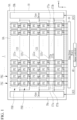
- FIG. 2 is a top layout view of two pixels of a display device constructed according to an example.
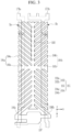
- FIG. 3 is a top plan view of a pixel electrode and data lines of FIG. 2 .
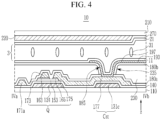
- FIG. 4 is a cross-sectional view taken along line IVa-IVb of the display device of FIG. 2 .
- the display panel 10 of the display device 1 includes a first substrate 110 and a second substrate 210 facing each other, and a liquid crystal layer 3 disposed between the first substrate 110 and the second substrate 210.
- a gate conductive layer including a gate line 121, a gate electrode 124, and a storage electrode line 131 may be disposed.
- the gate conductive layer may include metal, such as molybdenum (Mo), copper (Cu), aluminum (Al), magnesium (Mg), silver (Ag), gold (Au), platinum (Pt), palladium (Pd), nickel (Ni), neodymium (Nd), iridium (Ir), tungsten (W), titanium (Ti), chromium (Cr), tantalum (Ta), and alloys thereof.
- One gate line 121 may include a pair of line portions 122 and 123.
- a pair of line portions 122 and 123 may extend substantially in parallel to each other in the first direction x.
- the gate electrodes 124 are disposed between a pair of line portions 122 and 123, and the gate electrodes 124 may be directly connected to a pair of line portions 122 and 123.
- a pair of line portions 122 and 123 may be electrically connected to each other by the gate electrodes 124, and may transmit the same gate signal as each other.
- An opening 25 is formed in the gate line 121 between two neighboring gate electrodes 124 in the first direction x.
- a pair of line portions 122 and 123 of the gate line 121 may face and be substantially parallel with each other across the openings 25 in a region where the gate electrodes 124 are not disposed.
- the storage electrode line 131 is spaced apart from the gate line 121 and the gate electrode 124 in a plan view.
- the storage electrode line 131 may transmit a constant voltage, such as a common voltage.
- the storage electrode line 131 may include a main line 131a extending substantially in the first direction x, extensions 131b substantially extending in the second direction y and connected to the main line 131a, and extension portions 131c extending from a portion of the main line 131a.
- a pitch of the extensions 131b connected to the main line 131a in the first direction x and a pitch of the extension portions 131c in the first direction x may be substantially the same as the pitch of the pixels PX in the first direction x.
- a first insulating layer 140 may be disposed on the gate conductive layer.
- the first insulating layer 140 may include an inorganic insulating material, such as a silicon oxide (SiOx), a silicon nitride (SiNx), and the like.
- the first insulating layer 140 may also be referred to as a gate insulating layer.
- a semiconductor layer including semiconductors 153 and 156 are disposed on the first insulating layer 140.
- the semiconductor layer may include amorphous silicon, polysilicon, or an oxide semiconductor material.
- the semiconductor 153 may substantially overlap the gate electrode 124 in a plan view.
- Ohmic contact layers 163 and 165 may be disposed on the semiconductor 153.
- the ohmic contact layers 163 and 165 may include a material, such as n+ hydrogenated amorphous silicon, in which an n-type impurity such as a phosphor is doped at a high density, or a silicide.
- the ohmic contact layers 163 and 165 may be omitted.
- a data conductive layer including data lines 171a and 171b, a source electrode 173, and a drain electrode 175, may be disposed on the ohmic contact layers 163 and 165 and the first insulating layer 140.
- the data conductive layer may include metal, such as aluminum (Al), copper (Cu), magnesium (Mg), silver (Ag), gold (Au), platinum (Pt), palladium (Pd), nickel (Ni), neodymium (Nd), iridium (Ir), molybdenum (Mo), tungsten (W), titanium (Ti), chromium (Cr), tantalum (Ta), and alloys thereof.
- the data lines 171a and 171b extend substantially in the second direction y and may intersect the gate line 121.
- the data lines 171a and 171b may include a curved portion CV, and the curved portion CV may include a portion extending substantially in the first direction x and a portion extending substantially in the second direction y.
- One of the data lines 171a and 171b may be directly connected with the source electrodes 173.
- the source electrode 173 may extend from one of the data lines 171a and 171b toward the gate electrode 124 and may have a substantially "U" shape.
- the drain electrode 175 may include a portion that faces the source electrode 173 in a region overlapping with gate electrode 124, and an extension portion 177.
- the extension portion 177 may be disposed above the gate line 121 and the gate electrode 124 in a plan view. Most of the region between the drain electrode 175 and the source electrode 173 facing each other may overlap the semiconductor 153.
- the extension portion 177 may overlap the extension portion 131c of the storage electrode line 131.
- the extension portion 177 overlaps the extension portion 131c of the storage electrode line 131 via the first insulating layer 140 interposed therebetween to form a storage capacitor Cst.
- the storage capacitor Cst may maintain the voltage applied to the drain electrode 175 and a pixel electrode 191 connected thereto when no data voltage is applied to the data lines 171a and 171b.
- the gate electrode 124, the source electrode 173, and the drain electrode 175 form a transistor Q, which may function as a switching element, together with the semiconductor 153.
- the channel of the transistor Q is formed in the semiconductor 153 between the source electrode 173 and the drain electrode 175.
- One pixel PX may be electrically connected to at least one of the first data line 171a and the second data line 171b by the transistor Q.
- FIG. 2 exemplarily shows that the pixel PX is connected to the first data line 171a.
- the openings 25 in the gate line 121 overlap the data lines 171a and 171b in a planar view to reduce a signal delay due to coupling between the gate line 121 and the data lines 171a and 171b.
- Each semiconductor 156 may be disposed in a portion where the gate line 121, the gate electrode 124, or the storage electrode line 131, and the data lines 171a and 171b, are intersected, to prevent an electrical short between the gate conductive layer and the data conductive layer.
- the ohmic contact layers 163 and 165 may be only formed between the underlying semiconductor 153 and the data conductive layer thereon to reduce the contact resistance therebetween.
- the semiconductor 153 may have a portion that is not covered by the data conductive layer, such as a portion between the source electrode 173 and the drain electrode 175.
- a second insulating layer 180a may be disposed on the data conductive layer, and a third insulating layer 180b may be disposed on the second insulating layer 180a.
- the second insulating layer 180a and the third insulating layer 180b may include the inorganic insulating material and/or the organic insulating material.
- the second insulating layer 180a and the third insulating layer 180b include a contact hole 185 overlapping the extension portion 177 of the drain electrode 175.
- a color filter layer 230 may be disposed between the second insulating layer 180a and the third insulating layer 180b.
- the color filter layer 230 includes color filters having different colors, and each color filter may include a pigment that has the color represented by the corresponding pixel PX.
- the third insulating layer 180b may prevent a material of the color filter layer 230 from penetrating into the liquid crystal layer 3.
- the color filter layer 230 may include an opening 235 overlapping the contact hole 185 of the second insulating layer 180a and the third insulating layer 180b.
- the contact hole 185 may be disposed in the opening 235.
- two adjacent color filter layers 230 may partially overlap each other at the boundary between the pixels PX. More particularly, when each color filter layer 230 extends along each pixel column PXC, and one color filter layer 230 is disposed on one pixel column PXC, two color filter layers 230 may be partially overlapped with each other between the adjacent pixel columns PXC, and the region where two color filter layers 230 overlaps may overlap the extension 131b of the storage electrode line 131.
- a pixel electrode layer including a pixel electrode 191 and a shielding electrode 199 may be disposed on the third insulating layer 180b.
- the pixel electrode layer may include a transparent conductive material, such as ITO (indium tin oxide) and IZO (indium zinc oxide), or aluminum, silver, chromium, or alloys thereof.
- the pixel electrode 191 may have a substantially quadrangular shape with patterns formed therein.
- the pixel electrode 191 includes a transverse stem part 192, a longitudinal stem part 193, and branch parts 194.
- An extension 196 and an extension portion 197 may be connected to the pixel electrode 191.
- the transverse stem part 192 extends substantially in the first direction x, and the longitudinal stem part 193 extends substantially in the second direction y.
- the transverse stem part 192 includes a first transverse stem part 192a and a second transverse stem part 192b disposed on the left and right sides of the longitudinal stem part 193, respectively.
- the second transverse stem part 192b protrudes from the longitudinal stem part 193 substantially in the first direction x
- the first transverse stem part 192a protrudes from the longitudinal stem part 193 substantially in a direction opposite to the first direction x.
- the pixel electrode 191 may be divided into four sub-regions by the transverse stem part 192 and the longitudinal stem part 193. When the electric field is applied, the liquid crystal molecules 31 of the liquid crystal layer 3 in the four sub-regions may be inclined in different directions from each other, thus realizing a wide viewing angle.
- the width of the longitudinal stem part 193 in the first direction x may be substantially constant or may vary along the second direction y.
- the width of the transverse stem part 192 in the second direction y may be substantially constant or may vary along the first direction x.
- the branch parts 194 are disposed in four sub-regions and are connected to the transverse stem part 192 or the longitudinal stem part 193.
- the branch parts 194 may extend substantially in an oblique direction with respect to the first direction x and the second direction y, and from an acute angle of about 30° to about 60°, about 40° to about 50°, or about 45° with the first direction x or the second direction y.
- the branch parts 194 include first branch parts 194a and second branch parts 194b disposed on the left and right sides of the longitudinal stem part 193, respectively.
- the first branch parts 194a and the second branch parts 194b which face each other via the longitudinal stem part 193 therebetween, extend in different directions.
- the extending direction of the first branch parts 194a and the extending direction of the second branch parts 194b may be substantially symmetrical with respect to the longitudinal stem part 193.
- a first slit Sa which is the spacing slit, is disposed between neighboring first branch parts 194a.
- a second slit Sb is disposed between neighboring second branch parts 194b.
- the first slit Sa and the second slit Sb may have a substantially parallelogramical shape, respectively.
- the first electrode part 191a when the portion of the pixel electrode 191 disposed on the left of the longitudinal stem part 193 is referred to as a first electrode part 191a, the first electrode part 191a includes a first transverse stem part 192a and first branch parts 194a, and the first slits Sa are formed on the first electrode part 191a.
- the second electrode part 191b When the portion of the pixel electrode 191 disposed on the right of the longitudinal stem part 193 is referred to as a second electrode part 191b, the second electrode part 191b includes a second transverse stem part 192b and second branch parts 194b, and the second slits Sb are formed on the second electrode part 191b.
- the first electrode part 191a overlaps the first data line 171a and the second electrode part 191b overlaps the second data line 171b.
- the first slits Sa overlap the first data line 171a and the second slits Sb overlap the second data line 171b.
- a first width Wa of the first slits Sa is different from a second width Wb of the second slits Sb.
- the first width Wa refers to the width measured in a direction substantially perpendicular to the extending direction of the first slit Sa.
- the extending direction of the first slit Sa may be substantially parallel to the extending direction of the neighboring first branch parts 194a interposing the first slit Sa.
- the second width Wb refers to the width measured in a direction substantially perpendicular to the extending direction of the second slit Sb, and the extending direction of the second slit Sb may be substantially parallel to an extending direction of the neighboring second branch parts 194b interposing the second slit Sb.
- the width of the first branch parts 194a may be different from the width of the second branch parts 194b.
- the first electrode part 191a and the second electrode part 191b may have a substantially symmetrical shape, except that the first width Wa of the first slits Sa and the second width Wb of the second slits Sb are different.
- the first slits Sa and the second slits Sb may be substantially symmetric with respect to the longitudinal stem part 193, except that the first width Wa and the second width Wb are different.
- embodiments of the inventive concept are not limited thereto.
- the first slits Sa and the second slits Sb may be asymmetric with respect to the longitudinal stem part 193.
- the first width Wa of the first slits Sa may be substantially constant in the first electrode part 191a, and may be different depending on the position.
- the second width Wb of the second slits Sb may be substantially constant in the second electrode part 191b, and may be different depending on the position.
- the first width Wa and the second width Wb may be formed differently from each other to reduce the overlapping area between the slit and the data line, thereby suppressing the increase of the luminance due to the data field, which will be described in more detail below.
- the extension 196 includes a first extension 196a and a second extension 196b connected to the first electrode part 191a and the second electrode part 191b, respectively.
- the first extension 196a may extend from the first branch part 194a of first electrode part 191a
- the second extension 196b may extend from the second branch part 194b of the second electrode part 191b.
- the first extension 196a and the second extension 196b are connected to the extension portion 197 disposed therebetween.
- the extension portion 197 overlaps the extension portion 177 of the drain electrode 175 of the transistor Q in a plan view, and is connected to the extension portion 177 of the drain electrode 175 via the contact hole 185 to receive the data voltage.
- the end portions of the left and right edges of the pixel electrode 191 may not overlap the extensions 131b as shown in FIG. 2 , but in some exemplary embodiments, they may overlap with each other.
- the extensions 131b may include extensions overlapping the longitudinal stem part 193 of the pixel electrode 191 in some exemplary embodiments.
- the shielding electrode 199 is spaced apart from the pixel electrode 191 and may extend substantially in the first direction x, and may be positioned between two pixel rows PXR neighboring in the second direction y.
- the shielding electrode 199 overlaps at least part of the gate line 121 to prevent light leakage that may occur near the gate line 121.
- the shielding electrode which may be formed of the pixel electrode layer, may also be disposed on the extensions 131b of the storage electrode line 131.
- a light blocking member 220 may be disposed below the second substrate 210.
- the light blocking member 220 may block the light leakage between neighboring pixel electrodes 191.
- the light blocking member 220 may be disposed in a region between the pixel electrodes 191 neighboring in the second direction y, and may extend substantially in the first direction x. In a plan view, the light blocking member 220 may prevent the light leakage by covering most of the region where the transistor Q, the gate line 121, and the drain electrode 175 are disposed.
- the extension 131b of the storage electrode line 131 may block the light leakage between neighboring pixel electrodes 191 by overlapping most of the space between two pixel electrodes 191 neighboring in the first direction x.
- a common electrode 270 may be disposed under the second substrate 210 and the light blocking member 220.
- the common electrode 270 may be formed continuously at the portion of the region corresponding to the display area DA.
- the common electrode 270 may include the transparent conductive material, such as ITO or IZO, or aluminum, silver, chromium, or alloys thereof.
- the color filter layer 230 may be disposed below the second substrate 210, for example, between the second substrate 210 and the common electrode 270.
- the liquid crystal layer 3 may include liquid crystal molecules 31 having negative dielectric anisotropy. In some exemplary embodiments, however, the light crystal molecules 31 may have positive dielectric anisotropy.
- the liquid crystal molecules 31 may be oriented such that long axes thereof are substantially perpendicular or acute with respect to the surfaces of the first substrate 110 and the second substrate 210, when electric field is not applied in the liquid crystal layer 3.
- the liquid crystal molecules 31 may be pretilted according to the patterned portions of the pixel electrode 191 (e.g., a fringe field between the edge of the branch parts 194 and the common electrode 270).
- An alignment layer 11 may be disposed on the pixel electrode 191, and an alignment layer 21 may be disposed under the common electrode 270. Both alignment layers 11 and 21 may be vertical alignment layers. Polymer protrusions (bumps) including reactive mesogens reacting with light, such as ultraviolet rays, may be disposed on surfaces of the alignment layers 11 and 21 adjacent to the liquid crystal layer 3, such that the pretilt of the liquid crystal molecules 31 of the liquid crystal layer 3 may be maintained through the polymer protrusions.
- bumps including reactive mesogens reacting with light, such as ultraviolet rays
- the display device 1 when the data voltage is applied to the pixel electrode 191 and the common voltage is applied to the common electrode 270, an electric field is generated on the liquid crystal layer 3.
- the electric field includes a vertical component that is substantially perpendicular to the surfaces of the first substrate 110 and the second substrate 210, and a fringe field component that may be formed by the edge of the pattern of the transverse stem part 192, the longitudinal stem part 193, and the branch parts 194 of the pixel electrode 191.
- the liquid crystal molecules 31 may be tilted in a direction substantially parallel to the surfaces of the first substrate 110 and the second substrate 210 in response to the applied electric field, and in the region where the branch parts 194 are formed, the liquid crystal molecules 31 may be inclined toward the inside of each branch part 194 by the fringe field, and eventually be tilted in the direction substantially parallel to the extending direction of the branch parts 194. Accordingly, the liquid crystal layer 3 corresponding to each pixel electrode 191 may be divided into four regions having different directions in which the liquid crystal molecules 31 may be inclined. These four regions correspond to four sub-regions of the pixel electrode 191 described above.
- a pair of data lines 171a and 171b may be disposed to overlap the pixel electrode 191 in the corresponding pixel column PXC, which may reduce the risk of causing short and the crosstalk between the data lines 171a and 171b, and the change of the parasitic capacitance between the data lines 171a and 171b and pixel electrode 191 may be reduced or prevented.
- the electric field (hereinafter may be referred to as a "data field") caused by the data voltage transmitted through the data lines 171a and 171b may affect the liquid crystal layer 3 and distort the electric field in the liquid crystal layer 3. As such, the luminance of a specific region of the screen may be increased or decreased.
- FIG. 5 is a schematic view exemplarily illustrating the influence of a data field in a display device according to the principles of the invention.
- FIG. 6 is a schematic view exemplarily illustrating the relation of a slit of a pixel electrode and a data line in a display device according to the principles of the invention.
- FIG. 5 schematically shows only the relevant configurations to illustrate the effect of the data fields of the data lines 171a and 171b.
- the first data line 171a and the second data line 171b overlap the first electrode part 191a and the second electrode part 191b
- the first data line 171a and the second data line 171b overlap the first slits Sa and the second slits Sb, respectively.
- the data fields of the first data line 171a and the second data line 171b are not completely shielded due to the first slits Sa and the second slits Sb, and thus, may affect the electric field in the liquid crystal layer 3 through the first slits Sa and the second slits Sb. For example, when displaying a high gray after displaying a low gray in the second direction y, which is a sequential output direction of the gate signal, the effect of this data field may appear as an increase in luminance in the low gray display area.
- the first data line 171a may transmit a positive data voltage and the second data line 171b may transmit a negative data voltage.
- the pixel PX (hereinafter referred to as "a previous pixel") connected to the first data line 171a and receiving the positive data voltage (e.g., the data voltage of 10 V when the common voltage is 7.5 V) to display the low gray (e.g., about a gray of 25 to 32 in 255 grays) may be charged with the positive data voltage.
- the first region overlapping the first data line 171a may have an increased potential by a further higher positive data voltage (e.g., 15 V) applied to a different pixel PX (hereinafter "the next pixel") displaying the high gray, and thus, the luminance of the first region may be increased.
- the second region overlapping the second data line 171b may have a decreased potential by a lower negative data voltage (e.g., 0 V) applied to the next pixel displaying the high gray, and thus, the luminance of the second region may be decreased.
- the luminance of the second region overlapping the second data line 171b may be increased and the luminance of the first region overlapping the first data line 171a may be decreased.
- the influence of the luminance increase is greater than the luminance decrease, so the luminance of the previous pixel may be increased overall.
- the effect from the increase in luminance of the previous pixel is substantially the same when the electrically connected data line transmits the negative data voltage and the neighboring data line transmits the positive data voltage.
- the first data line 171a transmits the negative data voltage
- the second data line 171b transmits the positive data voltage.
- the potential of the first region may be decreased by the further lower negative data voltage applied to the next pixel. This is because the negative data voltage is charged in the previous pixel, the intensity of the electric field is increased. As such, the luminance of the first region may be increased.
- the potential of the second region may be increased by the further higher positive data voltage applied to the next pixel. This is because the negative data voltage is charged in the previous pixel, the intensity of the electric field decreases. As such, the luminance of the second region may be decreased. Accordingly, the luminance of the corresponding pixel PX may be increased overall, thereby deteriorating the image quality.
- the first width Wa is formed to be different from the second width Wb to prevent deterioration of an image from increased luminance caused by the overlap between the pixel electrode 191 with a pair of data lines 171a and 171b. More particularly, when the first width Wa is formed to be less than the second width Wb, the data field may be reduced in the region (e.g., the first region overlapping the first data line 171a electrically connected to the corresponding pixel PX among a pair of data lines 171a and 171b) that may have the increased luminance. When the corresponding pixel is electrically connected to the second data line 171b, the second width Wb may be formed to be less than the first width Wa, thereby suppressing the increase of the luminance.
- the influence of the data field may be controlled by varying the thickness of the insulating layer between a pair of data lines 171a and 171 b and the pixel electrode 191.
- the insulating layer of the region overlapping the data line electrically connected to the corresponding pixel may be formed thicker than the insulating layer of the region overlapping the data line that is not electrically connected to the corresponding pixel.
- the data field from the data line that is electrically connected to the corresponding pixel may be reduced.
- the thickness of the second insulating layer 180a and/or the third insulating layer 180b may be formed thicker in the region overlapping the first electrode part 191a than in the region overlapping the second electrode part 191b.
- the first width Wa of the first slit Sa is less than the second width Wb of the second slit Sb, and the area of the region Aa where the first slit Sa overlaps the first data line 171a is smaller than the area of the region Ab where the second slit Sb and the second data line 171b are overlapped. Accordingly, the first electrode part 191a formed with the first slit Sa may further shield from the data field than the second electrode part 191b formed with the second slit Sb.
- the influence from the increased luminance in the region overlapping the first data line 171a may be reduced, thereby substantially offsetting or reducing the change of luminance in the corresponding pixel.
- the above-described problem from increased luminance may also appear in the low gray display area, when displaying the low gray after displaying the high gray in the sequence output direction of the gate signal.
- the low gray display area of the particular frame increases or decreases the potential of the first region due to the higher positive data voltage or the lower negative data voltage applied to the high gray display area of the next frame, thereby increasing the luminance.
- the first width Wa of the first slit Sa and the second width Wb of the second slit Sb may be varied according to the principles of the invention described above to substantially offset or reduce the change of luminance in the corresponding pixel.
- FIG. 7 is a top layout view of four adjacent pixels of the display device 1 constructed according to an example, which is not falling under the scope of the claimed invention.
- FIG. 7 shows the structure in which the pixel electrodes 191 disposed in the pixel rows PXR are connected to a pair of data lines 171a and 171b as in FIG. 1 .
- the pixel electrode 191 of the upper pixel row PXR is electrically connected to the first transistor Qa electrically connected to the first sub-gate line 121a and the first data line 171a
- the pixel electrode 191 of the lower pixel row PXR is electrically connected to the second transistor Qb electrically connected to the second sub-gate line 121b and the second data line 171b.
- the width of the second slits Sb overlapping the second data line 171b may be less than the width of the first slits Sa overlapping the first data line 171a.
- the first sub-gate line 121a and the second sub-gate line 121b are electrically connected to each other to transmit the same gate signal.
- the pixel electrodes 191 of two pixel rows PXR neighboring in the second direction y may be alternately connected to the different data lines 171a and 171b through the transistors Qa and Qb.
- a pair of data lines 171a and 171b corresponding to one pixel column PXC may extend substantially in the second direction y across the pixel electrodes 191 of the corresponding pixel column PXC.
- FIG. 8 is a top plan view of a pixel electrode and data lines of one pixel of a display device of FIG. 7 according to an exemplary embodiment.
- the display device is substantially the same as the display device 1 described above, except the widths Wa1 and Wa2 of the first slit Sa of the first electrode part 191a are not substantially the same when the first data line 171a is electrically connected to the pixel electrode 191. More specifically, the first slit Sa includes a portion with a relatively wider width Wa1 and a portion with a relatively narrower width Wa2. In the first slit Sa, the portion with the width Wa2 overlaps the first data line 171a. The portion with the width Wa1 in the first slit Sa may not overlap the first data line 171a.
- the width Wa1 may be equal to or substantially equal to the width Wb of the second slit Sb of the second electrode part 191b.
- the widths Wa1 and Wa2 of the first slit Sa are formed relatively narrow only in the region overlapping the first data line 171a, while minimizing the design changes of the branch parts 194a and 194b of the pixel electrode 191, the area of the portion overlapping the first data line 171a in the first slit Sa may be reduced, thereby reducing the influence of the data field due to the first data line 171a electrically connected to the corresponding pixel PX.
- the widths Wa1 and Wa2 of the first slit Sa of the first electrode part 191a may be substantially the same as each other, and the width Wb of the second slit Sb of the second electrode part 191b may be formed to have at least two different widths, in which a relatively narrower one disposed in portion overlapping the second data line 171b.
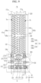
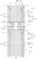
- FIG. 9 is a top layout view of one pixel of a display device of FIG. 7 according to an exemplary embodiment
- FIG. 10 is a top plan view of the pixel electrode and data lines in the pixel of FIG. 9
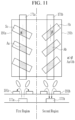
- FIG. 11 is a schematic view exemplary illustrating the relationship of a slit of a pixel electrode and a data line in a display device according to the principles of the invention.
- the display device is substantially the same as the display device of FIG. 2 and FIG. 3 , except for the shape of the pixel electrode 191.
- a first angle ⁇ which is an acute angle formed between the extending direction of the first slit Sa of the first electrode part 191a and the second direction y, is different from a second angle ⁇ formed between the extending direction of the second slit Sb of the second electrode part 191b and the second direction y.
- the extending direction of the first slit Sa corresponds to the extending direction of the first branch part 194a adjacent to the first slit Sa
- the extending direction of the second slit Sb corresponds to the extending direction of the second branch part 194b adjacent to the second slit Sb.
- the first angle ⁇ may be greater than the second angle ⁇ .
- the first branch parts 194a and the first slit Sa are more inclined toward the transverse stem part 192 than the second branch parts 194b and the second slit Sb.
- the first angle ⁇ may be greater than the second angle ⁇ by about 1° to about 30°, or about 5° to about 20°.
- the area of the first slit Sa overlapping the first data line 171a and the area of the second slit Sb overlapping the second data line 171b may also be different from each other.
- the width of the first slit Sa and the width of the second slit Sb are the same, when the first angle ⁇ is greater than the second angle ⁇ , the area of the region Aa where the first slit Sa and the first data line 171a are overlapped is smaller than the area of the region Ab where the second slit Sb and the second data line 171b are overlapped.
- the first electrode part 191a formed with the first slit Sa may shield the data field more than the second electrode part 191b formed with the second slit Sb, when the pixel electrode 191 is electrically connected to the first data line 171a to receive the data voltage from the first data line 171a, the luminance increase may be suppressed in the region overlapping the first data line 171a.
- the second angle ⁇ may be greater than the inclination first angle ⁇ of the first slit Sa.
- the first angle ⁇ and the second angle ⁇ are formed to be different with each other as shown in FIG. 9 and FIG. 10
- the first width Wa and the second width Wb are formed to be different with each other as shown in FIG. 2 and FIG. 3 , to suppress the luminance increase in the region overlapping the electrically connected data line of a pair of data lines 171a and 171b.
- the first angle ⁇ may be greater than the second angle ⁇ and the first width Wa may be less than the second width Wb.
- FIG. 12 is a top layout view of one pixel of a display device according to an example, which is not falling under the scope of the claimed invention
- FIG. 13 is an equivalent circuit diagram of a representative pixel shown in FIG. 12 .
- the display device according to this illustrated example is substantially similar to the display device described above, and thus, descriptions of substantially similar components will be omitted to avoid redundancy, and the differences will be mainly described.
- one pixel PX is divided into two subpixels sPX1 and sPX2, and the first data line 171a of a pair of data lines 171a and 171b overlapping the pixel PX is electrically connected to the pixel PX to improve lateral visibility.
- a first subpixel electrode 1911 and the second subpixel electrode 1912 are electrically connected to the first data line 171a.
- the pixel PX is connected to the gate line 121, the first data line 171a, and a reference voltage line 172.
- the pixel PX incudes the first subpixel sPX1 and the second subpixel sPX2.
- the first subpixel sPX1 includes the first transistor Qa, the first liquid crystal capacitor Clc1, and the first storage capacitor Cst1
- the second subpixel sPX2 includes the second transistor Qb, the third transistor Qc, the second liquid crystal capacitor Clc2, and the second storage capacitor Cst2.
- the first transistor Qa and the second transistor Qb are connected to the gate line 121 and the first data line 171a, respectively, and the third transistor Qc is connected to the output terminal of the second transistor Qb and the reference voltage line 172.
- the output terminal of the first transistor Qa is connected to the first liquid crystal capacitor Clc1 and the first storage capacitor Cst1, and the output terminal of the second transistor Qb is connected to the second liquid crystal capacitor Clc2, the second storage capacitor Cst2, and the input terminal of the third transistor Qc.
- the control terminal of the third transistor Qc is connected to the gate line 121, the input terminal thereof is connected to the second liquid crystal capacitor Clc2 and the second storage capacitor Cst2, and the output terminal is connected to the reference voltage line 172.
- the gate-on voltage is applied to the gate line 121, the first transistor Qa, the second transistor Qb, and the third transistor Qc are turned on.
- the data voltage applied to the first data line 171a is applied to the first liquid crystal capacitor Clc1 and the second liquid crystal capacitor Clc2 through the turned-on first transistor Qa and second transistor Qb, respectively, and the first liquid crystal capacitor Clc1 and the second liquid crystal capacitor Clc2 are charged to the difference between the data voltage and the common voltage.
- the same data voltage is applied to the first liquid crystal capacitor Clc1 and the second liquid crystal capacitor Clc2 through the first transistor Qa and the second transistor Qb, respectively, while the charging voltage of the second liquid crystal capacitor Clc2 is divided through the third transistor Qc. Therefore, the charging voltage of the second liquid crystal capacitor Clc2 becomes less than the charging voltage of the first liquid crystal capacitor Clc1, thereby differentiating the luminance of the two subpixels sPX1 and sPX2.
- the image viewed from the side may be made as close as possible to the image viewed from the front, thereby improving the lateral visibility.
- the first subpixel sPX1 includes the first subpixel electrode 1911
- the second subpixel sPX2 includes the second subpixel electrode 1912.
- the first subpixel electrode 1911 corresponds to one electrode of the first liquid crystal capacitor Clc1 described above
- the second subpixel electrode 1912 corresponds to one electrode of the second liquid crystal capacitor Clc2 described above.
- the gate line 121 which may include a pair of line portions 122 and 123, is disposed between the first subpixel electrode 1911 and the second subpixel electrode 1912.
- the first subpixel electrode 1911 includes a transverse stem part 1921, a longitudinal stem part 1931, and branch parts 1941.
- the transverse stem part 1921 includes a first transverse stem part 1921a and a second transverse stem part 1921b disposed on the left and right sides of the longitudinal stem part 1931, respectively.
- the branch parts 1941 include first branch parts 1941a and second branch parts 1941b disposed on the left and right sides of the longitudinal stem part 1931, respectively.
- the first slit S1a is disposed between neighboring first branch parts 1941a
- the second slit S1b is disposed between neighboring second branch parts 1941b.
- the first electrode part 1911a When a portion of the first subpixel electrode 1911 disposed on the left side of the longitudinal stem part 1931 is referred to as a first electrode part 1911a, the first electrode part 1911a includes the first transverse stem part 1921a and the first branch parts 1941a, and the first slits S1a are formed in the first electrode part 1911a.
- the second electrode part 1911b When a portion of the first subpixel electrode 1911 disposed on the right side of the longitudinal stem part 1931 is referred to as a second electrode part 1911b, the second electrode part 1911b includes the second transverse stem part 1921b and the second branch parts 1941b, and the second slits S1b are formed in the second electrode part 1911b.
- the second subpixel electrode 1912 includes a transverse stem part 1922, a longitudinal stem part 1932, and branch parts 1942.
- the transverse stem part 1922 includes a first transverse stem part 1922a and a second transverse stem part 1922b disposed on the left and right sides of the longitudinal stem part 1932, respectively.
- the branch parts 1942 include first branch parts 1942a and second branch parts 1942b disposed on the left and right sides of the longitudinal stem part 1932, respectively.
- the third slit S2a is disposed between neighboring first branch parts 1942a and the fourth slit S2b is disposed between neighboring second branch parts 1942b.
- a third electrode part 1912a includes the first transverse stem part 1922a and the first branch parts 1942a, and the third electrode part 1912a has the third slits S2a.
- a fourth electrode part 1912b includes the second transverse stem part 1922b and the second branch parts 1942b, and the fourth electrode part 1912b includes the fourth slits S2b.
- the first data line 171a overlaps the first electrode part 1911a and the first slits S1a of the first subpixel electrode 1911, and overlaps the third electrode part 1912a and the third slits S2a of the second subpixel electrode 1912.
- the second data line 171b overlaps the second electrode part 1911b and the second slits S1b of the first subpixel electrode 1911, and overlaps the fourth electrode part 1912b and the fourth slit S2b of the second subpixel electrode 1912).
- the first width W1a of the first slit S1a on the first subpixel electrode 1911 is different from the second width W1b of the second slit S1b.
- the third width S2a of the third slit S2a is different from the fourth width W2b of the fourth slit S2b.
- the second width W1b may be less than the first width W1a
- the fourth width W2b may be less than the third width W2a.
- the overlapping area between the slit and the data line may be reduced, for example, by relatively narrowing the width of the slit overlapping the data line which is electrically connected to the corresponding pixel PX among a pair of data lines 171a and 171b, and thus, the low gray display area may suppress the increase of the luminance due to the data field that may be caused by the data voltage applied to the high gray display area.
- FIG. 14 is a top layout view of one pixel of a display device according to an exemplary embodiment.
- the display device is substantially the same as the display device shown in FIG. 12 , except for the shapes of the first subpixel electrode 1911 and the second subpixel electrode 1912.
- the first angle ⁇ 1 as the acute angle between the extending direction of the first slit S1a of the first electrode part 1911a and the second direction y is different from the second angle ⁇ 1 as the acute angle between the extending direction of the second slit S1b of the second electrode part 1911b and the second direction y.
- the third angle ⁇ 2 as the acute angle between the extending direction of the third slit S2a of the third electrode part 1912a and the second direction y is different from the fourth angle ⁇ 2 as the acute angle between the extending direction of the fourth slit S2b of the fourth electrode part 1912b and the second direction y.
- the first angle ⁇ 1 may be greater than the second angle ⁇ 1
- the third angle ⁇ 2 maybe greater than the fourth angle ⁇ 2.
- the second angle ⁇ 1 may be greater than the first angle ⁇ 1
- the fourth angle ⁇ 2 may be greater than the third angle ⁇ 2.
- relatively increasing the angle of the slit overlapping the data line which is electrically connected to the corresponding pixel PX among a pair of data lines 171a and 171b may reduce the overlapping area between the slit and the data line, and thus, the low gray display area may suppress the increase of the luminance that may be caused from to the data voltage applied to the high gray display area.
- FIG. 15 is a top layout view of one pixel of a display device according to an example, which is not falling under the scope of the claimed invention
- FIG. 16 is an equivalent circuit diagram of a representative pixel shown in FIG. 15 .
- the display device according to this illustrated example is substantially similar to the display device described above, and thus, descriptions of substantially similar components will be omitted to avoid redundancy, and the differences will be mainly described.
- one pixel PX is divided into two subpixels sPX1 and sPX2, the first data line 171a of a pair of data lines 171a and 171b overlapping the pixel PX is electrically connected to the first subpixel sPX1, and the second data line 171b is electrically connected to the second subpixel sPX2 to improve side visibility.
- the pixel PX is connected to the gate line 121, the first data line 171a, and the second data line 171b.
- the pixel PX includes the first subpixel sPX1 and the second subpixel sPX2.
- the first subpixel sPX1 includes the first transistor Qa, the first liquid crystal capacitor Clc1, and the first storage capacitor Cst1
- the second subpixel sPX2 includes the second transistor Qb, the third transistor Qc, the second liquid crystal capacitor Clc2, and the second storage capacitor Cst2.
- the first transistor Qa includes the control terminal connected to the gate line 121 and the input terminal connected to the first data line 171a.
- the output terminal of the first transistor Qa is connected to the first liquid crystal capacitor Clc1 and the first storage capacitor Cst1.
- the second transistor Qb includes the control terminal connected to the gate line 121 and the input terminal connected to the second data line 171b.
- the output terminal of the second transistor Qb is connected to the second liquid crystal capacitor Clc2 and the second storage capacitor Cst2.
- the first liquid crystal capacitor Clc1 and the second liquid crystal capacitor Clc2 may receive different data voltages based on one image signal through the first transistor Qa and the second transistor Qb connected to the first data line 171a and the second data line 171b, respectively.
- the image viewed from the side may be made as close as possible to the image viewed from the front, thereby improving the lateral visibility.
- the first subpixel sPX1 includes the first subpixel electrode 1911
- the second subpixel sPX2 includes the second subpixel electrode 1912.
- the first subpixel electrode 1911 corresponds to one electrode of the first liquid crystal capacitor Clc1 described above
- the second subpixel electrode 1912 corresponds to one electrode of the second liquid crystal capacitor Clc2 described above.
- the first subpixel electrode 1911 includes a transverse stem part 1921, a longitudinal stem part 1931, and branch parts 1941.
- the transverse stem part 1921 includes a first transverse stem part 1921a and a second transverse stem part 1921b disposed on the left and right sides of the longitudinal stem part 1931, respectively.
- the branch parts 1941 include first branch parts 1941a and second branch parts 1941b disposed on the left and right sides of the longitudinal stem part 1931, respectively.
- a first slit S1a is disposed between neighboring first branch parts 1941a and a second slit S1b is disposed between neighboring second branch parts 1941b.
- the first electrode part 1911a When a portion of the first subpixel electrode 1911 disposed on the left side of the longitudinal stem part 1931 is referred to as a first electrode part 1911a, the first electrode part 1911a includes a first transverse stem part 1921a and first branch parts 1941a, and the first slits S1a are formed on the first electrode part 1911a.
- the second electrode part 1911b When a portion of the first subpixel electrode 1911 disposed on the right side of the longitudinal stem part 1931 is referred to as the second electrode part 1911b, the second electrode part 1911b includes a second transverse stem part 1921b and second branch parts 1941b, and the slits S1b are formed on the second electrode part 1911b.
- the second subpixel electrode 1912 includes the transverse stem part 1922, the longitudinal stem part 1932, and branch parts 1942.
- the transverse stem part 1922 includes a first transverse stem part 1922a and a second transverse stem part 1922b disposed on the left and right sides of the longitudinal stem part 1932, respectively.
- the branch parts 1942 include first branch parts 1942a and second branch parts 1942b disposed on the left and right sides of the longitudinal stem part 1932, respectively.
- a third slit S2a is disposed between neighboring first branch parts 1942a, and a fourth slit S2b is disposed between neighboring second branch parts 1942b.
- the third electrode part 1912a includes a first transverse stem part 1922a and first branch parts 1942a, and the third electrode part 1912a has third slits S2a.
- the fourth electrode part 1912b includes the second transverse stem part 1922b and the second branch parts 1942b, and the fourth electrode part 1912b includes the fourth slits S2b.
- the first data line 171a overlaps the first electrode part 1911a and the first slits S1a of the first subpixel electrode 1911, and overlaps the third electrode part 1912a and the third slits S2a of the second subpixel electrode 1912.
- the second data line 171b overlaps the second electrode part 1911b and the second slits S1b of the first subpixel electrode 1911, and overlaps the fourth electrode part 1912b and the fourth slit S2b of the second subpixel electrode 1912.
- the first width W1a of the first slit S1a in the first subpixel electrode 1911 is different from the second width W1b of the second slit S1b.
- the third width W2a of the third slit S2a in the second subpixel electrode 1912 is different from the fourth the width W2b of the fourth slit S2b.
- the first data line 171a is electrically connected to the first subpixel electrode 1911, and the second data line 171b is electrically connected to the second subpixel electrode 1912.
- the first subpixel sPX1 increases the luminance in the region overlapping the first data line 171a
- the second subpixel sPX2 increases the luminance in the region overlapping the second data line 171b.
- Such an increase in the luminance increase may be particularly problematic when the first data line 171a and the second data line 171b transmit the data voltages of different polarities, for substantially the same reasons described above with reference to FIG. 5 .
- the first width W1a may be less than the second width W1b, and the fourth width W2b may be less than the third width W2a, to suppress the increase in luminance.
- the second width W1b when the second data line 171b is electrically connected to the first subpixel electrode 1911 and the first data line 171a is electrically connected to the second subpixel electrode 1912, the second width W1b may be less than the first width W1a and the third the width W2a may be smaller than the fourth width W2b.
- the low gray display area may suppress the increase of the luminance due to the data field which may be caused from the data voltage applied to the high gray display area.
- FIG. 17 is a top layout view of one pixel of a display device according to an exemplary embodiment.
- the display device is substantially the same as the display device shown in FIG. 15 , except for the shapes of the first subpixel electrode 1911 and the second subpixel electrode 1912.
- the first angle ⁇ 1 as the acute angle between the extending direction of the first slit S1a of the first electrode part 1911a and the second direction y is different from the second angle ⁇ 1 as the acute angle between the extending direction of the second slit S1b of the second electrode part 1911b and the second direction y.
- the third angle ⁇ 2 as the acute angle between the extending direction of the third slit S2a of the third electrode part 1912a and the second direction y is different from the fourth angle ⁇ 2 as the acute angle between the extending direction of the fourth slit S2b of the fourth electrode part 1912b and the second direction y.
- the first angle ⁇ 1 may be greater than the second angle ⁇ 1
- the fourth angle ⁇ 2 may be greater than the third angle ⁇ 2.
- the second angle ⁇ 1 may be greater than the first angle ⁇ 1
- the third angle ⁇ 2 may be greater than the fourth angle ⁇ 2.
- the low gray display area may suppress the increase of the luminance due to the data voltage applied to the high gray display area, thereby preventing deterioration in the image quality of a display device.
- Embodiments of the invention provide a display device comprising: a first pixel electrode including a first electrode part having a first slit and a second electrode part having a second slit; and a first data line and a second data line overlapping the first pixel electrode, the first and second data lines being adjacent to each other in a first direction, wherein: the first data line overlaps the first electrode part and the first slit, and the second data line overlaps the second electrode part and the second slit; and a first area defined by a first overlapping region between the first slit and the first data line is different from a second area defined by a second overlapping region between the second slit and the second data line.
- the first pixel electrode may comprise a longitudinal stem part and a plurality of first branch parts extending from one side of the longitudinal stem part and a plurality of second branch parts extending from another side of the longitudinal stem part.
- the first slit may be formed between two adjacent first branch parts, and the second slit may be formed between two adjacent second branch parts. There may be a plurality of first and second slits.
- the longitudinal stem part may generally extend in the same direction as the first and second data line.
- the first pixel electrode may further includes a transverse stem part extending in a direction crossing the longitudinal stem part.
- One or more first branch parts and/or one or more second branch parts may extend from the transverse stem part.
Landscapes
- Physics & Mathematics (AREA)
- Nonlinear Science (AREA)
- Mathematical Physics (AREA)
- Chemical & Material Sciences (AREA)
- Crystallography & Structural Chemistry (AREA)
- General Physics & Mathematics (AREA)
- Optics & Photonics (AREA)
- Engineering & Computer Science (AREA)
- Microelectronics & Electronic Packaging (AREA)
- Spectroscopy & Molecular Physics (AREA)
- Geometry (AREA)
- Liquid Crystal (AREA)
- Devices For Indicating Variable Information By Combining Individual Elements (AREA)
Claims (10)
- Anzeigevorrichtung (1), umfassend:eine erste Pixelelektrode (191), die einen ersten Elektrodenteil (191a) mit einem ersten Spalt (Sa) und einen zweiten Elektrodenteil (191b) mit einem zweiten Spalt (Sb) aufweist; undeine erste Datenleitung (171a) und eine zweite Datenleitung (171b), wobei die erste und die zweite Datenleitung (171a, 171b) in einer ersten Richtung zueinander benachbart sind, wobei die erste Pixelelektrode (191) die erste Datenleitung (171a) und die zweite Datenleitung (171b) überlappt,wobei:der erste Elektrodenteil (191a) und der erste Spalt (Sa) die erste Datenleitung (171a) überlappen und der zweite Elektrodenteil (191b) und der zweite Spalt (Sb) die zweite Datenleitung (171b) überlappen;eine erste Fläche, definiert durch einen ersten Überlappungsbereich (Aa) zwischen dem ersten Spalt (Sa) und der ersten Datenleitung (171a), sich von einer zweiten Fläche, definiert durch einen zweiten Überlappungsbereich (Ab) zwischen dem zweiten Spalt (Sb) und der zweiten Datenleitung (171b), unterscheidet;die erste Datenleitung (171a) elektrisch an die erste Pixelelektrode (191a) angeschlossen ist; undder erste Spalt (Sa) eine erste Breite (Wa) aufweist und der zweite Spalt (Sb) eine zweite Breite (Wb) aufweist, wobei die erste Breite (Wa) des ersten Spaltes (Sa) kleiner als die zweite Breite (Wb) des zweiten Spaltes (Sb) ist,dadurch gekennzeichnet, dass der erste Spalt (Sa) einen ersten Spaltabschnitt mit der ersten Breite (Wa2) und einen zweiten Spaltabschnitt mit einer dritten Breite (Wa1), die größer als die erste Breite ist, aufweist; undder erste Spaltabschnitt die erste Datenleitung (171a) überlappt und der zweite Spaltabschnitt die erste Datenleitung (171a) nicht überlappt.
- Anzeigevorrichtung (1) nach Anspruch 1, ferner umfassend eine zweite Pixelelektrode, die der ersten Pixelelektrode in einer zweiten Richtung, die die erste Richtung schneidet, benachbart ist,
wobei die zweite Datenleitung (171b) elektrisch an die zweite Pixelelektrode angeschlossen ist. - Anzeigevorrichtung (1) nach Anspruch 2, wobei:die zweite Pixelelektrode einen ersten Elektrodenteil und einen zweiten Elektrodenteil aufweist, die in der zweiten Richtung entsprechend auf den ersten Elektrodenteil und den zweiten Elektrodenteil der ersten Pixelelektrode ausgerichtet sind; undin der zweiten Pixelelektrode der erste Elektrodenteil einen ersten Spalt aufweist, der zweite Elektrodenteil einen zweiten Spalt aufweist und eine Breite des zweiten Spaltes kleiner als eine Breite des ersten Spaltes ist.
- Anzeigevorrichtung (1) nach Anspruch 2 oder 3, ferner umfassend eine Gate-Leitung (121), sie sich im Wesentlichen in die erste Richtung erstreckt,
wobei die Gate-Leitung eine erste Unter-Gate-Leitung (121a), die elektrisch an die erste Pixelelektrode angeschlossen ist, und eine zweite Unter-Gate-Leitung (121b), die elektrisch an die zweite Pixelelektrode angeschlossen ist, aufweist. - Anzeigevorrichtung (1) nach einem der Ansprüche 1 bis 4, wobei:die erste Pixelelektrode (191) ferner einen Querstammteil (192), einen Längsstammteil (193), der den Querstammteil schneidet, und eine Mehrzahl von Zweigteilen (194), die sich von dem Querstammteil oder dem Längsstammteil aus erstrecken, aufweist; undder erste Elektrodenteil (191a) auf einer Seite des Längsstammteils angeordnet ist und der zweite Elektrodenteil (191b) auf der anderen Seite des Längsstammteils angeordnet ist.
- Anzeigevorrichtung (1) nach Anspruch 5, wobei der erste Spalt (Sa) und der zweite Spalt (Sb) in einem Abstand zwischen benachbarten Zweigteilen der Mehrzahl von Zweigteilen (194) beabstandet sind.
- Anzeigevorrichtung (1) nach Anspruch 5 oder 6, wobei der erste Spalt (Sa) und der zweite Spalt (Sb) bezüglich des Längsstammteils (193) symmetrisch angeordnet sind.
- Anzeigevorrichtung (1) nach einem der Ansprüche 1 bis 7, wobei die erste Datenleitung (171a) und die zweite Datenleitung (171b) dazu ausgestaltet sind, Datenspannungen mit Polaritäten, die sich voneinander unterscheiden, während eines Frames zu übertragen.
- Anzeigevorrichtung (1), umfassend:eine erste Pixelelektrode (191), die einen ersten Elektrodenteil (191a) mit einem ersten Spalt (Sa) und einen zweiten Elektrodenteil (191b) mit einem zweiten Spalt (Sb) aufweist; undeine erste Datenleitung (171a) und eine zweite Datenleitung (171b), wobei die erste und die zweite Datenleitung (171a, 171b) in einer ersten Richtung zueinander benachbart sind, wobei die erste Pixelelektrode (191) die erste Datenleitung (171a) und die zweite Datenleitung (171b) überlappt,wobei:die erste Pixelelektrode ferner aufweist: einen Querstammteil (192), einen Längsstammteil (193), der den Querstammteil schneidet, und eine Mehrzahl von Zweigteilen (194), die sich von dem Querstammteil oder dem Längsstammteil aus erstrecken;der erste Elektrodenteil (191a) auf einer Seite des Längsstammteils (193) angeordnet ist und der zweite Elektrodenteil (191b) auf der anderen Seite des Längsstammteils (193) angeordnet ist;der erste Spalt und der zweite Spalt bezüglich des Längsstammteils symmetrisch angeordnet sind;der erste Elektrodenteil und der erste Spalt die erste Datenleitung überlappen und der zweite Elektrodenteil und der zweite Spalt die zweite Datenleitung überlappen;eine erste Fläche, definiert durch einen ersten Überlappungsbereich (Aa) zwischen dem ersten Spalt und der ersten Datenleitung, sich von einer zweiten Fläche, definiert durch einen zweiten Überlappungsbereich (Ab) zwischen dem zweiten Spalt und der zweiten Datenleitung, unterscheidet;die erste Datenleitung (171a) elektrisch an die erste Pixelelektrode (191) angeschlossen ist;dadurch gekennzeichnet, dass ein erster spitzer Winkel (α), definiert zwischen der Erstreckungsrichtung des ersten Spaltes und einer zweiten Richtung, die lotrecht zu der ersten Richtung verläuft, sich von einem zweiten spitzen Winkel (β), definiert zwischen der Erstreckungsrichtung des zweiten Spaltes und der zweiten Richtung, unterscheidet;
undder erste spitze Winkel größer als der zweite spitze Winkel ist. - Anzeigevorrichtung (1) nach Anspruch 9, ferner umfassend:eine zweite Pixelelektrode (1912), die der ersten Pixelelektrode in der zweiten Richtung, die die erste Richtung schneidet, benachbart ist,wobei:die zweite Datenleitung (171b) elektrisch an die zweite Pixelelektrode angeschlossen ist;die zweite Pixelelektrode (1912) einen ersten Elektrodenteil (1912a) und einen zweiten Elektrodenteil (1912b) aufweist, die in der zweiten Richtung entsprechend auf den ersten Elektrodenteil und den zweiten Elektrodenteil der ersten Pixelelektrode ausgerichtet sind; undin der zweiten Pixelelektrode der erste Elektrodenteil einen ersten Spalt (S2a) aufweist, der zweite Elektrodenteil einen zweiten Spalt (S2b) aufweist und ein dritter spitzer Winkel, definiert zwischen der Erstreckungsrichtung des zweiten Spaltes und der zweiten Richtung, größer ist als ein vierter spitzer Winkel, definiert zwischen der Erstreckungsrichtung des ersten Spaltes und der zweiten Richtung.
Applications Claiming Priority (1)
| Application Number | Priority Date | Filing Date | Title |
|---|---|---|---|
| KR1020180121117A KR102583805B1 (ko) | 2018-10-11 | 2018-10-11 | 표시 장치 |
Publications (2)
| Publication Number | Publication Date |
|---|---|
| EP3637181A1 EP3637181A1 (de) | 2020-04-15 |
| EP3637181B1 true EP3637181B1 (de) | 2023-09-20 |
Family
ID=68280777
Family Applications (1)
| Application Number | Title | Priority Date | Filing Date |
|---|---|---|---|
| EP19202593.0A Active EP3637181B1 (de) | 2018-10-11 | 2019-10-10 | Elektrodenkonfiguration für eine flüssigkristallanzeige |
Country Status (4)
| Country | Link |
|---|---|
| US (1) | US20200117062A1 (de) |
| EP (1) | EP3637181B1 (de) |
| KR (2) | KR102583805B1 (de) |
| CN (1) | CN111045258B (de) |
Families Citing this family (8)
| Publication number | Priority date | Publication date | Assignee | Title |
|---|---|---|---|---|
| KR102567013B1 (ko) * | 2018-10-17 | 2023-08-14 | 삼성디스플레이 주식회사 | 액정 표시 장치 |
| KR20210044340A (ko) * | 2019-10-14 | 2021-04-23 | 삼성디스플레이 주식회사 | 표시 장치 |
| KR102848665B1 (ko) * | 2020-04-27 | 2025-08-25 | 삼성디스플레이 주식회사 | 표시 장치 |
| CN112750853B (zh) * | 2021-02-09 | 2022-09-20 | 南昌广恒电子中心(有限合伙) | 像素结构、显示基板和显示装置 |
| CN121122183A (zh) * | 2021-04-30 | 2025-12-12 | 京东方科技集团股份有限公司 | 显示基板以及显示装置 |
| CN114879418A (zh) * | 2022-07-11 | 2022-08-09 | 惠科股份有限公司 | 阵列基板及显示面板 |
| CN114879419B (zh) * | 2022-07-11 | 2022-10-25 | 惠科股份有限公司 | 阵列基板及显示面板 |
| CN115877618B (zh) * | 2022-12-29 | 2024-11-01 | Tcl华星光电技术有限公司 | 显示面板及显示装置 |
Family Cites Families (10)
| Publication number | Priority date | Publication date | Assignee | Title |
|---|---|---|---|---|
| KR101215512B1 (ko) * | 2006-08-21 | 2012-12-26 | 삼성디스플레이 주식회사 | 액정표시장치 |
| JP5103494B2 (ja) * | 2010-03-05 | 2012-12-19 | 株式会社ジャパンディスプレイイースト | 液晶表示装置 |
| CN102955300B (zh) * | 2011-08-31 | 2015-05-27 | 群康科技(深圳)有限公司 | 液晶面板 |
| TWI542932B (zh) | 2014-07-22 | 2016-07-21 | 友達光電股份有限公司 | 顯示面板及曲面顯示器 |
| KR102242229B1 (ko) * | 2014-07-29 | 2021-04-21 | 삼성디스플레이 주식회사 | 액정표시장치 |
| CN204406004U (zh) * | 2015-03-06 | 2015-06-17 | 京东方科技集团股份有限公司 | 阵列基板和显示装置 |
| TWI564641B (zh) * | 2015-05-22 | 2017-01-01 | 友達光電股份有限公司 | 畫素結構及具有此畫素結構的畫素陣列 |
| KR102446004B1 (ko) * | 2015-12-31 | 2022-09-22 | 삼성디스플레이 주식회사 | 액정 표시 장치 |
| TWI581043B (zh) | 2016-10-04 | 2017-05-01 | 友達光電股份有限公司 | 畫素結構 |
| CN110178170B (zh) * | 2017-01-16 | 2021-12-07 | 株式会社半导体能源研究所 | 显示装置 |
-
2018
- 2018-10-11 KR KR1020180121117A patent/KR102583805B1/ko active Active
-
2019
- 2019-10-10 EP EP19202593.0A patent/EP3637181B1/de active Active
- 2019-10-10 US US16/598,073 patent/US20200117062A1/en not_active Abandoned
- 2019-10-11 CN CN201910963025.4A patent/CN111045258B/zh active Active
-
2023
- 2023-09-22 KR KR1020230127130A patent/KR102650551B1/ko active Active
Also Published As
| Publication number | Publication date |
|---|---|
| KR102583805B1 (ko) | 2023-09-27 |
| CN111045258B (zh) | 2025-05-16 |
| EP3637181A1 (de) | 2020-04-15 |
| CN111045258A (zh) | 2020-04-21 |
| KR20230142412A (ko) | 2023-10-11 |
| KR20200041410A (ko) | 2020-04-22 |
| US20200117062A1 (en) | 2020-04-16 |
| KR102650551B1 (ko) | 2024-03-22 |
Similar Documents
| Publication | Publication Date | Title |
|---|---|---|
| EP3637181A1 (de) | Elektrodenkonfiguration für eine flüssigkristallanzeige | |
| USRE46497E1 (en) | Liquid crystal display apparatus having data lines with curved portions and method | |
| US8941789B2 (en) | Liquid crystal display | |
| CN110297368B (zh) | 显示装置 | |
| KR101319595B1 (ko) | 액정 표시 장치 | |
| US11054706B2 (en) | Display device | |
| US20040085495A1 (en) | Liquid crystal display | |
| US9395592B2 (en) | Display device | |
| US9551905B2 (en) | Display device | |
| US10775676B2 (en) | Display device | |
| US9989818B2 (en) | Liquid crystal display device | |
| US20170192312A1 (en) | Liquid crystal display device | |
| US9373647B2 (en) | Thin film transistor array panel and liquid crystal display including the same | |
| US11579502B2 (en) | Display device | |
| KR101502358B1 (ko) | 액정 표시 장치 | |
| KR102756672B1 (ko) | 액정 표시 장치 | |
| US11106094B2 (en) | Liquid crystal display | |
| US11215892B2 (en) | Display device |
Legal Events
| Date | Code | Title | Description |
|---|---|---|---|
| PUAI | Public reference made under article 153(3) epc to a published international application that has entered the european phase |
Free format text: ORIGINAL CODE: 0009012 |
|
| STAA | Information on the status of an ep patent application or granted ep patent |
Free format text: STATUS: THE APPLICATION HAS BEEN PUBLISHED |
|
| AK | Designated contracting states |
Kind code of ref document: A1 Designated state(s): AL AT BE BG CH CY CZ DE DK EE ES FI FR GB GR HR HU IE IS IT LI LT LU LV MC MK MT NL NO PL PT RO RS SE SI SK SM TR |
|
| AX | Request for extension of the european patent |
Extension state: BA ME |
|
| STAA | Information on the status of an ep patent application or granted ep patent |
Free format text: STATUS: REQUEST FOR EXAMINATION WAS MADE |
|
| 17P | Request for examination filed |
Effective date: 20201013 |
|
| RBV | Designated contracting states (corrected) |
Designated state(s): AL AT BE BG CH CY CZ DE DK EE ES FI FR GB GR HR HU IE IS IT LI LT LU LV MC MK MT NL NO PL PT RO RS SE SI SK SM TR |
|
| STAA | Information on the status of an ep patent application or granted ep patent |
Free format text: STATUS: EXAMINATION IS IN PROGRESS |
|
| 17Q | First examination report despatched |
Effective date: 20220210 |
|
| GRAP | Despatch of communication of intention to grant a patent |
Free format text: ORIGINAL CODE: EPIDOSNIGR1 |
|
| STAA | Information on the status of an ep patent application or granted ep patent |
Free format text: STATUS: GRANT OF PATENT IS INTENDED |
|
| INTG | Intention to grant announced |
Effective date: 20230414 |
|
| P01 | Opt-out of the competence of the unified patent court (upc) registered |
Effective date: 20230516 |
|
| GRAS | Grant fee paid |
Free format text: ORIGINAL CODE: EPIDOSNIGR3 |
|
| GRAA | (expected) grant |
Free format text: ORIGINAL CODE: 0009210 |
|
| STAA | Information on the status of an ep patent application or granted ep patent |
Free format text: STATUS: THE PATENT HAS BEEN GRANTED |
|
| AK | Designated contracting states |
Kind code of ref document: B1 Designated state(s): AL AT BE BG CH CY CZ DE DK EE ES FI FR GB GR HR HU IE IS IT LI LT LU LV MC MK MT NL NO PL PT RO RS SE SI SK SM TR |
|
| REG | Reference to a national code |
Ref country code: GB Ref legal event code: FG4D |
|
| REG | Reference to a national code |
Ref country code: CH Ref legal event code: EP |
|
| REG | Reference to a national code |
Ref country code: NL Ref legal event code: FP |
|
| REG | Reference to a national code |
Ref country code: IE Ref legal event code: FG4D |
|
| REG | Reference to a national code |
Ref country code: DE Ref legal event code: R096 Ref document number: 602019037733 Country of ref document: DE |
|
| REG | Reference to a national code |
Ref country code: LT Ref legal event code: MG9D |
|
| PG25 | Lapsed in a contracting state [announced via postgrant information from national office to epo] |
Ref country code: GR Free format text: LAPSE BECAUSE OF FAILURE TO SUBMIT A TRANSLATION OF THE DESCRIPTION OR TO PAY THE FEE WITHIN THE PRESCRIBED TIME-LIMIT Effective date: 20231221 |
|
| PG25 | Lapsed in a contracting state [announced via postgrant information from national office to epo] |
Ref country code: SE Free format text: LAPSE BECAUSE OF FAILURE TO SUBMIT A TRANSLATION OF THE DESCRIPTION OR TO PAY THE FEE WITHIN THE PRESCRIBED TIME-LIMIT Effective date: 20230920 Ref country code: RS Free format text: LAPSE BECAUSE OF FAILURE TO SUBMIT A TRANSLATION OF THE DESCRIPTION OR TO PAY THE FEE WITHIN THE PRESCRIBED TIME-LIMIT Effective date: 20230920 Ref country code: NO Free format text: LAPSE BECAUSE OF FAILURE TO SUBMIT A TRANSLATION OF THE DESCRIPTION OR TO PAY THE FEE WITHIN THE PRESCRIBED TIME-LIMIT Effective date: 20231220 Ref country code: LV Free format text: LAPSE BECAUSE OF FAILURE TO SUBMIT A TRANSLATION OF THE DESCRIPTION OR TO PAY THE FEE WITHIN THE PRESCRIBED TIME-LIMIT Effective date: 20230920 Ref country code: LT Free format text: LAPSE BECAUSE OF FAILURE TO SUBMIT A TRANSLATION OF THE DESCRIPTION OR TO PAY THE FEE WITHIN THE PRESCRIBED TIME-LIMIT Effective date: 20230920 Ref country code: HR Free format text: LAPSE BECAUSE OF FAILURE TO SUBMIT A TRANSLATION OF THE DESCRIPTION OR TO PAY THE FEE WITHIN THE PRESCRIBED TIME-LIMIT Effective date: 20230920 Ref country code: GR Free format text: LAPSE BECAUSE OF FAILURE TO SUBMIT A TRANSLATION OF THE DESCRIPTION OR TO PAY THE FEE WITHIN THE PRESCRIBED TIME-LIMIT Effective date: 20231221 Ref country code: FI Free format text: LAPSE BECAUSE OF FAILURE TO SUBMIT A TRANSLATION OF THE DESCRIPTION OR TO PAY THE FEE WITHIN THE PRESCRIBED TIME-LIMIT Effective date: 20230920 |
|
| REG | Reference to a national code |
Ref country code: AT Ref legal event code: MK05 Ref document number: 1613853 Country of ref document: AT Kind code of ref document: T Effective date: 20230920 |
|
| PG25 | Lapsed in a contracting state [announced via postgrant information from national office to epo] |
Ref country code: IS Free format text: LAPSE BECAUSE OF FAILURE TO SUBMIT A TRANSLATION OF THE DESCRIPTION OR TO PAY THE FEE WITHIN THE PRESCRIBED TIME-LIMIT Effective date: 20240120 |
|
| PG25 | Lapsed in a contracting state [announced via postgrant information from national office to epo] |
Ref country code: AT Free format text: LAPSE BECAUSE OF FAILURE TO SUBMIT A TRANSLATION OF THE DESCRIPTION OR TO PAY THE FEE WITHIN THE PRESCRIBED TIME-LIMIT Effective date: 20230920 |
|
| PG25 | Lapsed in a contracting state [announced via postgrant information from national office to epo] |
Ref country code: ES Free format text: LAPSE BECAUSE OF FAILURE TO SUBMIT A TRANSLATION OF THE DESCRIPTION OR TO PAY THE FEE WITHIN THE PRESCRIBED TIME-LIMIT Effective date: 20230920 |
|
| PG25 | Lapsed in a contracting state [announced via postgrant information from national office to epo] |
Ref country code: SM Free format text: LAPSE BECAUSE OF FAILURE TO SUBMIT A TRANSLATION OF THE DESCRIPTION OR TO PAY THE FEE WITHIN THE PRESCRIBED TIME-LIMIT Effective date: 20230920 Ref country code: RO Free format text: LAPSE BECAUSE OF FAILURE TO SUBMIT A TRANSLATION OF THE DESCRIPTION OR TO PAY THE FEE WITHIN THE PRESCRIBED TIME-LIMIT Effective date: 20230920 Ref country code: IS Free format text: LAPSE BECAUSE OF FAILURE TO SUBMIT A TRANSLATION OF THE DESCRIPTION OR TO PAY THE FEE WITHIN THE PRESCRIBED TIME-LIMIT Effective date: 20240120 Ref country code: ES Free format text: LAPSE BECAUSE OF FAILURE TO SUBMIT A TRANSLATION OF THE DESCRIPTION OR TO PAY THE FEE WITHIN THE PRESCRIBED TIME-LIMIT Effective date: 20230920 Ref country code: EE Free format text: LAPSE BECAUSE OF FAILURE TO SUBMIT A TRANSLATION OF THE DESCRIPTION OR TO PAY THE FEE WITHIN THE PRESCRIBED TIME-LIMIT Effective date: 20230920 Ref country code: CZ Free format text: LAPSE BECAUSE OF FAILURE TO SUBMIT A TRANSLATION OF THE DESCRIPTION OR TO PAY THE FEE WITHIN THE PRESCRIBED TIME-LIMIT Effective date: 20230920 Ref country code: AT Free format text: LAPSE BECAUSE OF FAILURE TO SUBMIT A TRANSLATION OF THE DESCRIPTION OR TO PAY THE FEE WITHIN THE PRESCRIBED TIME-LIMIT Effective date: 20230920 Ref country code: SK Free format text: LAPSE BECAUSE OF FAILURE TO SUBMIT A TRANSLATION OF THE DESCRIPTION OR TO PAY THE FEE WITHIN THE PRESCRIBED TIME-LIMIT Effective date: 20230920 Ref country code: PT Free format text: LAPSE BECAUSE OF FAILURE TO SUBMIT A TRANSLATION OF THE DESCRIPTION OR TO PAY THE FEE WITHIN THE PRESCRIBED TIME-LIMIT Effective date: 20240122 |
|
| PG25 | Lapsed in a contracting state [announced via postgrant information from national office to epo] |
Ref country code: PL Free format text: LAPSE BECAUSE OF FAILURE TO SUBMIT A TRANSLATION OF THE DESCRIPTION OR TO PAY THE FEE WITHIN THE PRESCRIBED TIME-LIMIT Effective date: 20230920 Ref country code: IT Free format text: LAPSE BECAUSE OF FAILURE TO SUBMIT A TRANSLATION OF THE DESCRIPTION OR TO PAY THE FEE WITHIN THE PRESCRIBED TIME-LIMIT Effective date: 20230920 |
|
| REG | Reference to a national code |
Ref country code: CH Ref legal event code: PL |
|
| REG | Reference to a national code |
Ref country code: BE Ref legal event code: MM Effective date: 20231031 |
|
| PG25 | Lapsed in a contracting state [announced via postgrant information from national office to epo] |
Ref country code: LU Free format text: LAPSE BECAUSE OF NON-PAYMENT OF DUE FEES Effective date: 20231010 |
|
| REG | Reference to a national code |
Ref country code: DE Ref legal event code: R097 Ref document number: 602019037733 Country of ref document: DE |
|
| PG25 | Lapsed in a contracting state [announced via postgrant information from national office to epo] |
Ref country code: LU Free format text: LAPSE BECAUSE OF NON-PAYMENT OF DUE FEES Effective date: 20231010 |
|
| PG25 | Lapsed in a contracting state [announced via postgrant information from national office to epo] |
Ref country code: MC Free format text: LAPSE BECAUSE OF FAILURE TO SUBMIT A TRANSLATION OF THE DESCRIPTION OR TO PAY THE FEE WITHIN THE PRESCRIBED TIME-LIMIT Effective date: 20230920 |
|
| PG25 | Lapsed in a contracting state [announced via postgrant information from national office to epo] |
Ref country code: DK Free format text: LAPSE BECAUSE OF FAILURE TO SUBMIT A TRANSLATION OF THE DESCRIPTION OR TO PAY THE FEE WITHIN THE PRESCRIBED TIME-LIMIT Effective date: 20230920 |
|
| PG25 | Lapsed in a contracting state [announced via postgrant information from national office to epo] |
Ref country code: CH Free format text: LAPSE BECAUSE OF NON-PAYMENT OF DUE FEES Effective date: 20231031 |
|
| PLBE | No opposition filed within time limit |
Free format text: ORIGINAL CODE: 0009261 |
|
| STAA | Information on the status of an ep patent application or granted ep patent |
Free format text: STATUS: NO OPPOSITION FILED WITHIN TIME LIMIT |
|
| PG25 | Lapsed in a contracting state [announced via postgrant information from national office to epo] |
Ref country code: MC Free format text: LAPSE BECAUSE OF FAILURE TO SUBMIT A TRANSLATION OF THE DESCRIPTION OR TO PAY THE FEE WITHIN THE PRESCRIBED TIME-LIMIT Effective date: 20230920 Ref country code: DK Free format text: LAPSE BECAUSE OF FAILURE TO SUBMIT A TRANSLATION OF THE DESCRIPTION OR TO PAY THE FEE WITHIN THE PRESCRIBED TIME-LIMIT Effective date: 20230920 Ref country code: CH Free format text: LAPSE BECAUSE OF NON-PAYMENT OF DUE FEES Effective date: 20231031 |
|
| 26N | No opposition filed |
Effective date: 20240621 |
|
| PG25 | Lapsed in a contracting state [announced via postgrant information from national office to epo] |
Ref country code: BE Free format text: LAPSE BECAUSE OF NON-PAYMENT OF DUE FEES Effective date: 20231031 |
|
| PG25 | Lapsed in a contracting state [announced via postgrant information from national office to epo] |
Ref country code: IE Free format text: LAPSE BECAUSE OF NON-PAYMENT OF DUE FEES Effective date: 20231010 |
|
| PG25 | Lapsed in a contracting state [announced via postgrant information from national office to epo] |
Ref country code: SI Free format text: LAPSE BECAUSE OF FAILURE TO SUBMIT A TRANSLATION OF THE DESCRIPTION OR TO PAY THE FEE WITHIN THE PRESCRIBED TIME-LIMIT Effective date: 20230920 |
|
| PG25 | Lapsed in a contracting state [announced via postgrant information from national office to epo] |
Ref country code: SI Free format text: LAPSE BECAUSE OF FAILURE TO SUBMIT A TRANSLATION OF THE DESCRIPTION OR TO PAY THE FEE WITHIN THE PRESCRIBED TIME-LIMIT Effective date: 20230920 Ref country code: IE Free format text: LAPSE BECAUSE OF NON-PAYMENT OF DUE FEES Effective date: 20231010 |
|
| PG25 | Lapsed in a contracting state [announced via postgrant information from national office to epo] |
Ref country code: BG Free format text: LAPSE BECAUSE OF FAILURE TO SUBMIT A TRANSLATION OF THE DESCRIPTION OR TO PAY THE FEE WITHIN THE PRESCRIBED TIME-LIMIT Effective date: 20230920 |
|
| PG25 | Lapsed in a contracting state [announced via postgrant information from national office to epo] |
Ref country code: BG Free format text: LAPSE BECAUSE OF FAILURE TO SUBMIT A TRANSLATION OF THE DESCRIPTION OR TO PAY THE FEE WITHIN THE PRESCRIBED TIME-LIMIT Effective date: 20230920 |
|
| PG25 | Lapsed in a contracting state [announced via postgrant information from national office to epo] |
Ref country code: CY Free format text: LAPSE BECAUSE OF FAILURE TO SUBMIT A TRANSLATION OF THE DESCRIPTION OR TO PAY THE FEE WITHIN THE PRESCRIBED TIME-LIMIT; INVALID AB INITIO Effective date: 20191010 |
|
| PG25 | Lapsed in a contracting state [announced via postgrant information from national office to epo] |
Ref country code: HU Free format text: LAPSE BECAUSE OF FAILURE TO SUBMIT A TRANSLATION OF THE DESCRIPTION OR TO PAY THE FEE WITHIN THE PRESCRIBED TIME-LIMIT; INVALID AB INITIO Effective date: 20191010 |
|
| PGFP | Annual fee paid to national office [announced via postgrant information from national office to epo] |
Ref country code: NL Payment date: 20250922 Year of fee payment: 7 |
|
| PGFP | Annual fee paid to national office [announced via postgrant information from national office to epo] |
Ref country code: GB Payment date: 20250922 Year of fee payment: 7 |
|
| PGFP | Annual fee paid to national office [announced via postgrant information from national office to epo] |
Ref country code: FR Payment date: 20250925 Year of fee payment: 7 |
|
| PG25 | Lapsed in a contracting state [announced via postgrant information from national office to epo] |
Ref country code: TR Free format text: LAPSE BECAUSE OF FAILURE TO SUBMIT A TRANSLATION OF THE DESCRIPTION OR TO PAY THE FEE WITHIN THE PRESCRIBED TIME-LIMIT Effective date: 20230920 |
|
| PGFP | Annual fee paid to national office [announced via postgrant information from national office to epo] |
Ref country code: DE Payment date: 20250922 Year of fee payment: 7 |