EP3633941B1 - Korrekturvorrichtung und korrekturverfahren - Google Patents
Korrekturvorrichtung und korrekturverfahren Download PDFInfo
- Publication number
- EP3633941B1 EP3633941B1 EP17915766.4A EP17915766A EP3633941B1 EP 3633941 B1 EP3633941 B1 EP 3633941B1 EP 17915766 A EP17915766 A EP 17915766A EP 3633941 B1 EP3633941 B1 EP 3633941B1
- Authority
- EP
- European Patent Office
- Prior art keywords
- module
- channel
- analog
- adjustment
- signal
- Prior art date
- Legal status (The legal status is an assumption and is not a legal conclusion. Google has not performed a legal analysis and makes no representation as to the accuracy of the status listed.)
- Active
Links
Images


Classifications
-
- H—ELECTRICITY
- H04—ELECTRIC COMMUNICATION TECHNIQUE
- H04B—TRANSMISSION
- H04B7/00—Radio transmission systems, i.e. using radiation field
- H04B7/02—Diversity systems; Multi-antenna system, i.e. transmission or reception using multiple antennas
- H04B7/04—Diversity systems; Multi-antenna system, i.e. transmission or reception using multiple antennas using two or more spaced independent antennas
- H04B7/06—Diversity systems; Multi-antenna system, i.e. transmission or reception using multiple antennas using two or more spaced independent antennas at the transmitting station
- H04B7/0686—Hybrid systems, i.e. switching and simultaneous transmission
-
- H—ELECTRICITY
- H04—ELECTRIC COMMUNICATION TECHNIQUE
- H04L—TRANSMISSION OF DIGITAL INFORMATION, e.g. TELEGRAPHIC COMMUNICATION
- H04L25/00—Baseband systems
- H04L25/38—Synchronous or start-stop systems, e.g. for Baudot code
- H04L25/40—Transmitting circuits; Receiving circuits
- H04L25/49—Transmitting circuits; Receiving circuits using code conversion at the transmitter; using predistortion; using insertion of idle bits for obtaining a desired frequency spectrum; using three or more amplitude levels ; Baseband coding techniques specific to data transmission systems
-
- H—ELECTRICITY
- H04—ELECTRIC COMMUNICATION TECHNIQUE
- H04B—TRANSMISSION
- H04B7/00—Radio transmission systems, i.e. using radiation field
- H04B7/02—Diversity systems; Multi-antenna system, i.e. transmission or reception using multiple antennas
- H04B7/04—Diversity systems; Multi-antenna system, i.e. transmission or reception using multiple antennas using two or more spaced independent antennas
- H04B7/06—Diversity systems; Multi-antenna system, i.e. transmission or reception using multiple antennas using two or more spaced independent antennas at the transmitting station
- H04B7/0613—Diversity systems; Multi-antenna system, i.e. transmission or reception using multiple antennas using two or more spaced independent antennas at the transmitting station using simultaneous transmission
- H04B7/0615—Diversity systems; Multi-antenna system, i.e. transmission or reception using multiple antennas using two or more spaced independent antennas at the transmitting station using simultaneous transmission of weighted versions of same signal
- H04B7/0617—Diversity systems; Multi-antenna system, i.e. transmission or reception using multiple antennas using two or more spaced independent antennas at the transmitting station using simultaneous transmission of weighted versions of same signal for beam forming
-
- H—ELECTRICITY
- H04—ELECTRIC COMMUNICATION TECHNIQUE
- H04L—TRANSMISSION OF DIGITAL INFORMATION, e.g. TELEGRAPHIC COMMUNICATION
- H04L27/00—Modulated-carrier systems
- H04L27/32—Carrier systems characterised by combinations of two or more of the types covered by groups H04L27/02, H04L27/10, H04L27/18 or H04L27/26
- H04L27/34—Amplitude- and phase-modulated carrier systems, e.g. quadrature-amplitude modulated carrier systems
- H04L27/36—Modulator circuits; Transmitter circuits
- H04L27/366—Arrangements for compensating undesirable properties of the transmission path between the modulator and the demodulator
- H04L27/367—Arrangements for compensating undesirable properties of the transmission path between the modulator and the demodulator using predistortion
-
- H—ELECTRICITY
- H03—ELECTRONIC CIRCUITRY
- H03F—AMPLIFIERS
- H03F1/00—Details of amplifiers with only discharge tubes, only semiconductor devices or only unspecified devices as amplifying elements
- H03F1/32—Modifications of amplifiers to reduce non-linear distortion
-
- H—ELECTRICITY
- H03—ELECTRONIC CIRCUITRY
- H03F—AMPLIFIERS
- H03F1/00—Details of amplifiers with only discharge tubes, only semiconductor devices or only unspecified devices as amplifying elements
- H03F1/32—Modifications of amplifiers to reduce non-linear distortion
- H03F1/3241—Modifications of amplifiers to reduce non-linear distortion using predistortion circuits
-
- H—ELECTRICITY
- H03—ELECTRONIC CIRCUITRY
- H03F—AMPLIFIERS
- H03F3/00—Amplifiers with only discharge tubes or only semiconductor devices as amplifying elements
- H03F3/20—Power amplifiers, e.g. Class B amplifiers, Class C amplifiers
- H03F3/24—Power amplifiers, e.g. Class B amplifiers, Class C amplifiers of transmitter output stages
-
- H—ELECTRICITY
- H04—ELECTRIC COMMUNICATION TECHNIQUE
- H04L—TRANSMISSION OF DIGITAL INFORMATION, e.g. TELEGRAPHIC COMMUNICATION
- H04L27/00—Modulated-carrier systems
- H04L27/32—Carrier systems characterised by combinations of two or more of the types covered by groups H04L27/02, H04L27/10, H04L27/18 or H04L27/26
- H04L27/34—Amplitude- and phase-modulated carrier systems, e.g. quadrature-amplitude modulated carrier systems
- H04L27/36—Modulator circuits; Transmitter circuits
- H04L27/362—Modulation using more than one carrier, e.g. with quadrature carriers, separately amplitude modulated
- H04L27/364—Arrangements for overcoming imperfections in the modulator, e.g. quadrature error or unbalanced I and Q levels
Definitions
- This application relates to the field of communications technologies, and in particular, to a correction apparatus and a correction method.
- the non-ideal channel may be, for example, a circuit with features such as nonlinearity, IQ imbalance, channel flatness, a channel delay error, a channel group delay ripple.
- Some elements in the circuit are easily affected by factors such as an environment and work in an abnormal state. Therefore, a signal in the circuit may be interfered, and an interference signal is introduced.
- a typical correction method is to dispose a correction circuit between an input end of the single signal channel and each non-ideal channel.
- a correction calculation module in the correction circuit obtains, through calculation, a correction parameter to adjust the global circuit, and then sends the correction parameter to a correction unit on the single signal channel, so that the correction unit uses the correction parameter to adjust an obtained signal, to adjust output signals of all the non-ideal channels and alleviate interference from the interference signal.
- US 2011/235749 A1 describes an antenna array having analogue transmitter linearization.
- Embodiments of this application provide a correction apparatus and a correction method, to improve efficiency of adjusting an error value of circuit signal.
- the embodiments of this application provide a correction apparatus and a correction method, to improve efficiency of adjusting an error value of circuit signal.
- the correction apparatus and the correction method provided in the embodiments of this application may be applied to a plurality of architectures.
- a feature of these architectures is that a plurality of non-ideal channels are driven by a single signal channel.
- the architectures each include one channel for transmitting a drive signal, and the channel is connected to the plurality of non-ideal channels.
- the non-ideal channel is such a channel that an output signal obtained in response to a drive signal has an error value.
- a response from an actual hardware circuit of the non-ideal channel within an operating frequency band is not an expected fixed value but is affected by a noise factor. After the non-ideal channel obtains the drive signal, the output signal of the non-ideal channel has the error value.
- the noise factor includes but is not limited to one or more factors such as a frequency (a frequency response), a time (a time change and a memory effect), a temperature (a temperature change), and a size of an input signal (nonlinear).
- the non-ideal channel includes but is not limited to channels of nonlinearity, IQ (quadrature complex signal) imbalance, channel flatness, a channel delay error, a channel group delay ripple, and the like.
- the architecture is decomposed into a channel for transmitting a drive signal and a plurality of analog channels, and adjustment is separately performed on the channel for transmitting a drive signal and the plurality of non-ideal channels, so that error values of output signals of the non-ideal channels are corrected.
- Such a model decomposition manner can reduce resource consumption and improve correction performance.
- correction parts of the non-ideal channels can reduce differences between the non-ideal channels, to further improve correction performance.
- the non-ideal channel having the nonlinearity may be, for example, an analog channel.
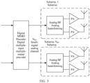
- an HBF Hybrid Beamforming, hybrid beamforming
- the HBF architecture includes a digital channel and a plurality of analog channels connected to the digital channel. An output end of the analog channel is connected to an antenna.
- the analog channel includes a power amplifier. Because the power amplifier has nonlinearity, the analog channel has nonlinearity. In other words, after the analog channel obtains a drive signal, an output response of the analog channel has nonlinearity.
- the nonlinearity of the power amplifier indicates that: nonlinear distortion is gradually generated as an input power of the power amplifier increases, and further a new frequency component is generated, affecting signal quality and interfering with another device.
- Linearization of the power amplifier means alleviating impact of nonlinearity on radio frequency performance by using various means, and maintaining relatively high amplifier efficiency as much as possible.
- a signal obtained by the analog channel in the embodiments of this application is a radio frequency signal. Therefore, the power amplifier disposed on the analog channel may be a radio frequency power amplifier.
- Main methods include a power back-off technology, an analog predistortion technology, and a DPD (Digital Pre-Distortion, digital predistortion) technology.
- the digital predistortion technology can not only greatly improve device efficiency, but also can ensure relatively good signal quality. Therefore, the digital predistortion technology is most widely applied.
- a linearization technology for a multi-channel architecture is required due to application of a MIMO (Multi-Input Multi-Output, multiple-input multiple-output) technology.
- MIMO in the 3rd/4th mobile communications systems widely uses a DBF (Digital Beamforming, digital beamforming) architecture. Therefore, linearization of a multi-channel architecture can be implemented through simple extension of a single-channel architecture.
- DBF Digital Beamforming, digital beamforming
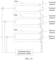
- FIG. 2 For a schematic diagram of the DBF architecture, refer to FIG. 2 .
- FIG. 1 For the schematic diagram of the HBF architecture, refer to FIG. 1 .
- FIG. 3 For detailed illustration of the HBF architecture, refer to FIG. 3 .
- beamforming and MIMO in a device of the HBF architecture are implemented through two-level weighting.
- a first level is digital weighting, and a second level may be analog weighting or digital weighting.
- the device of the HBF architecture includes the following network elements:
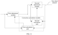
- FIG. 4 is a schematic structural diagram of a correction apparatus according to an embodiment of this application.
- the correction apparatus includes a first adjustment module, a plurality of second adjustment modules, a correction calculation module, and a plurality of non-ideal channels.
- One second adjustment module is disposed on one non-ideal channel.
- the first adjustment module is connected to each non-ideal channel.
- the correction calculation module is separately connected to the first adjustment module and the plurality of second adjustment modules.
- the correction calculation module is connected to an output end of each non-ideal channel.
- the non-ideal channel is such a channel that an output signal output in response to a drive signal has an error value.
- There are a plurality of factors that cause the error value of the output signal of the non-ideal channel for example, an ambient temperature and a circuit cable layout length. For details, refer to the foregoing descriptions of some specific scenarios of the non-ideal channel.
- the correction calculation module is configured to obtain a first adjustment parameter and a second adjustment parameter through calculation based on the output signal of the non-ideal channel and a reference signal.
- the reference signal is obtained based on the drive signal.
- the reference signal may be the drive signal or a signal from the drive signal.
- the first adjustment module is configured to adjust the drive signal based on the first adjustment parameter, to uniformly correct error values of output signals of the plurality of non-ideal channels.
- the second adjustment module on each non-ideal channel is configured to adjust a channel signal based on the second adjustment parameter, to correct a part that is of the error value and that is not corrected by the first adjustment module.
- the channel signal is a signal that is input to the non-ideal channel after the first adjustment module adjusts the drive signal.
- signals first pass through the first adjustment module, and are adjusted by the first adjustment module; and then, separately enter different non-ideal channels, and are adjusted by the second adjustment modules on the non-ideal channels, so that the output signals are output from the non-ideal channels in response to the signals adjusted by the first adjustment module and the second adjustment module.
- a channel on which the first adjustment module is located may be referred to as a drive channel.
- the drive channel is connected to the plurality of non-ideal channels, and provides channel signals for the plurality of non-ideal channels.
- the correction calculation module in the correction apparatus further performs a correction method. As shown in FIG. 5 , the method includes the following steps.
- Step 501 The correction calculation module obtains the output signal of the non-ideal channel and the reference signal.
- the reference signal is obtained based on the drive signal.
- the reference signal may be, for example, a drive signal obtained by a digital predistortion module, or the reference signal includes the drive signal and the input signal of the non-ideal channel.
- the input signal of the non-ideal channel comes from the drive signal adjusted by the first adjustment module.
- Step 502 The correction calculation module obtains the first adjustment parameter and the second adjustment parameter through calculation based on the output signal of the non-ideal channel and the reference signal.
- the output signal of the non-ideal channel is an actual output signal of the non-ideal channel.
- the reference signal belongs to a signal that has not yet been input to the non-ideal channel.
- the output signal is obtained based on the reference signal, so that a preset output signal of the non-ideal channel can be obtained based on the reference signal.
- the preset output signal is an output signal that does not have an error value on the non-ideal channel. Therefore, correction parameters: the first adjustment parameter and the second adjustment parameter are obtained based on the preset output signal and the actual output signal of the non-ideal channel.
- the reference signal includes the drive signal.
- the correction calculation may obtain the first adjustment parameter and the second adjustment parameter through calculation based on the output signal of the non-ideal channel and the drive signal obtained by the first adjustment module.
- the reference signal includes the drive signal and the input signal of the non-ideal channel.
- the correction calculation may obtain the first adjustment parameter through calculation based on the output signal of the non-ideal channel and the drive signal obtained by the first adjustment module, and the correction calculation module may obtain the second adjustment parameter through calculation based on an output signal and an input signal that belong to a same non-ideal channel.
- different non-ideal channels may have different second adjustment parameters.
- the first adjustment module is connected to the plurality of non-ideal channels, the first adjustment module adjusts a same error value of the plurality of non-ideal channels by adjusting the drive signal, and after the adjustment performed by the first adjustment module, the second adjustment module further adjusts an error value of a non-ideal channel to which the second adjustment module belongs. Therefore, the correction calculation module may output different second adjustment parameters to different non-ideal channels.
- the correction calculation needs to obtain different second adjustment parameters through calculation based on parameters (for example, output signals or input signals) of different non-ideal channels and output the second adjustment parameters to corresponding non-ideal channels.
- Step 503 The correction calculation module outputs the first adjustment parameter to the first adjustment module.
- the correction calculation module outputs the first adjustment parameter to the first adjustment module, so that the first adjustment module adjusts the drive signal based on the first adjustment parameter, to uniformly correct the error values of the output signals of the plurality of non-ideal channels.
- Step 504 The correction calculation module outputs the second adjustment parameter to the second adjustment module on each non-ideal channel.
- the correction calculation module outputs the second adjustment parameter to the second adjustment module on each non-ideal channel, so that the second adjustment module on each non-ideal channel adjusts the channel signal based on the second adjustment parameter, to correct a part that is of the error value and that is not corrected by the first adjustment module.
- the channel signal is a signal that is input to the non-ideal channel after the first adjustment module adjusts the drive signal.
- the first adjustment module adjusts the drive signal based on the first adjustment parameter, to uniformly correct the error values of the output signals of the plurality of non-ideal channels in advance, so that the first adjustment module performs error adjustment for the first time on the output signals of the plurality of non-ideal channels connected to the first adjustment module.
- the non-ideal channels may be different, and the error values of the output signals of the different non-ideal channels may be different.
- the first adjustment module can only uniformly adjust the error values for the plurality of non-ideal channels, that is, perform the same correction on the error values for the plurality of non-ideal channels.
- the second adjustment module on each non-ideal channel adjusts the channel signal based on the second adjustment parameter, to correct in advance the part that is of the error value and that is not corrected by the first adjustment module.
- complementary correction is performed on the error value of the output signal of each non-ideal channel, to eliminate the differences between the error values for the plurality of non-ideal channels.
- the first adjustment parameter and the second adjustment parameter are obtained by the correction calculation module through calculation based on the output signal of the non-ideal channel and the reference signal obtained based on the drive signal.
- the first adjustment module and the second adjustment module respectively obtain the first adjustment parameter and the second adjustment parameter from the correction calculation module.
- the first adjustment module uniformly corrects the error values of the output signals of the plurality of non-ideal channels.
- the second adjustment module performs complementary correction on the error value of the output signal of a non-ideal channel to which the second adjustment module belongs, to correct the part that is of the error value and that is not corrected by the first adjustment module. In this way, the error values of the output signals of the plurality of non-ideal channels are eliminated.
- the two adjustment modules cooperate with each other, to improve efficiency of adjusting an error value of circuit signal.
- Signal adjustment performed by the first adjustment module and the second adjustment module belongs to pre-adjustment.
- the signal of the correction apparatus is adjusted, so that a signal with a reduced error value is output on the non-ideal channel based on the adjusted signal. For example, if an output response of a non-ideal channel is not made based on the signal pre-adjusted by the first adjustment module and the second adjustment module, an error value of the output signal of the non-ideal channel is an increase of a preset value X when being affected by a noise factor.
- the signal in the correction apparatus is pre-adjusted by the first adjustment module and the second adjustment module.
- the error value of the output signal of the non-ideal channel based on the pre-adjusted signal is a decrease of a preset value X. Therefore, pre-adjustment operations of the first adjustment module and the second adjustment module may alleviate impact of the noise factor on an output result.
- the error value of the output signal of the non-ideal channel based on the signal pre-adjusted by the first adjustment module and the second adjustment module is neutralized in the effect of the noise factor, to reduce or eliminate the error value.
- the first adjustment module needs to obtain the first adjustment parameter, to adjust the obtained drive signal based on the first adjustment parameter.
- the first adjustment module needs to obtain the first adjustment parameter from the correction calculation module.
- the correction calculation module obtains the first adjustment parameter through calculation based on the output signal of the non-ideal channel and the reference signal.
- the reference signal is obtained based on the drive signal.
- the reference signal may be the drive signal obtained by the first adjustment module.
- the second adjustment module needs to obtain the second adjustment parameter, to adjust the channel signal based on the second adjustment parameter.
- the second adjustment module needs to obtain the second adjustment parameter from the correction calculation module.
- the correction calculation module may obtain the second adjustment parameter through calculation based on the output signal of the non-ideal channel and the reference signal.
- the reference signal is the drive signal obtained by the first adjustment module.
- the reference signal is the input signal of the non-ideal channel, and the input signal of the non-ideal channel comes from the drive signal adjusted by the first adjustment module.
- the correction calculation module analyzes the output signal of the non-ideal channel and the reference signal, determines whether the output signal of the non-ideal channel has the error value and how to adjust the error value, indicates, by using the first and the second adjustment parameters, information about adjusting the error value, outputs the first adjustment parameter to the first adjustment module, and outputs the second adjustment parameter to the second adjustment module.
- the two adjustment modules may adjust the signal, and accurately correct the error value of the output signal of the non-ideal channel.
- the correction calculation module is specifically implemented in a plurality of manners, for example, in an integrated manner or in a separated manner.
- the correction calculation module may obtain the first adjustment parameter and the second adjustment parameter through calculation on a same module.
- the correction calculation module is a chip.
- the correction calculation module may include two calculation units. One calculation unit is configured to calculate the first adjustment parameter, and the other calculation unit is configured to calculate the second adjustment parameter.
- the reference signal includes the drive signal and the input signal of the non-ideal channel.
- the correction calculation module includes a first calculation unit and a second calculation unit. The first calculation unit is connected to the first adjustment module. The second calculation unit is connected to the second adjustment module, and the second calculation unit is further connected to an input end of the non-ideal channel.
- the first calculation unit is configured to obtain the first adjustment parameter through calculation based on the output signal of the non-ideal channel and the drive signal.
- the second calculation unit is configured to obtain the second adjustment parameter through calculation based on an output signal and an input signal that belong to a same non-ideal channel.
- first calculation unit and the second calculation unit may be independent of each other and are not connected with a line, or the first calculation unit and the second calculation unit may be connected to each other with and exchange data, to cooperate with each other to more accurately calculate the first adjustment parameter and the second adjustment parameter.
- FIG. 6 shows only one non-ideal channel.
- the second adjustment module on each non-ideal channel is connected to the second calculation unit.
- the second calculation unit may be connected to a plurality of second adjustment modules and connected to input ends and output ends of the plurality of non-ideal channels.
- the second calculation unit obtains the second adjustment parameter through calculation based on the output signal and the input signal that belong to the same non-ideal channel; and then outputs, to the second adjustment module on the non-ideal channel, the second adjustment parameter obtained based on the signal of the non-ideal channel.
- the correction calculation module may include a plurality of second calculation units.
- one second calculation unit is configured for the second adjustment module on each non-ideal channel.
- One non-ideal channel is used as an example.
- a target second calculation unit is connected to an input end and an output end of a target non-ideal channel.
- the target second calculation unit is further connected to a target second adjustment module on the target non-ideal channel.
- the target second calculation unit obtains a second adjustment parameter through calculation based on an output signal and an input signal of the target non-ideal channel, and then outputs the second adjustment parameter to the target second adjustment module, so that the second adjustment module adjusts an error value on the target non-ideal channel based on the second adjustment parameter.
- the second calculation unit may not be connected to the input end of the non-ideal channel.
- the second calculation unit cooperates with the first calculation unit, and obtains a second adjustment parameter applicable to the target non-ideal channel through calculation based on the drive signal and the output signal of the target non-ideal channel.
- the second calculation obtains a preset output signal of the target non-ideal channel through calculation based on the drive signal; compares the preset output signal with an actual output signal of the non-ideal channel to obtain a value that needs to be adjusted; then obtains a correction parameter of the first calculation unit for the drive signal, for example, the first adjustment parameter; and obtains the second adjustment parameter through calculation based on the correction parameter and the value that needs to be adjusted.
- the correction calculation module may be connected to the input end of each non-ideal channel, or may not be connected to the input end.
- the step in which the correction calculation module obtains the first adjustment parameter and the second adjustment parameter through calculation based on the output signal of the non-ideal channel and the reference signal includes: obtaining, by the first calculation unit, the first adjustment parameter through calculation based on the output signal of the non-ideal channel and the drive signal; and obtaining, by the second calculation unit, the second adjustment parameter through calculation based on the output signal and the input signal that belong to the same non-ideal channel.
- the correction apparatus disposed in the separated manner can make the correction apparatus and the correction method provided in the embodiments of this application more flexible to implement and can facilitate circuit manufacturing.
- the correction apparatus and the correction method in the embodiments of this application may be applied in a plurality of scenarios, for example, the foregoing described scenarios of nonlinearity, IQ imbalance, channel flatness, a channel delay error, a channel group delay ripple, and the like.
- correction apparatus in this embodiment of this application may be applied to devices such as a base station and a Wi-Fi (Wireless-Fidelity, wireless fidelity) router.
- Wi-Fi Wireless-Fidelity, wireless fidelity
- the correction apparatus in the embodiment shown in FIG. 4 may be applied to the HBF architecture.
- the correction apparatus and the correction method in the embodiments of this application are used in the HBF architecture, to improve output linearity and efficiency of a power amplifier.
- the first adjustment module is a digital predistortion module
- the second adjustment module is a nonlinear adjustment module
- the correction calculation module is a hybrid beamforming HBF predistortion calculation module
- the first adjustment parameter is a digital predistortion parameter
- the second adjustment parameter is an analog nonlinear correction parameter
- the drive signal is a digital I/Q complex signal
- the non-ideal channel is an analog channel
- the channel signal is a radio frequency signal.
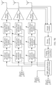
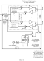
- the correction apparatus includes a digital channel and a plurality of analog channels.
- the digital channel is separately connected to the plurality of analog channels.
- the correction apparatus further includes a correction channel.
- the correction channel may obtain an output signal of an analog channel.
- a digital gain adjustment module, a digital phase adjustment module, a digital predistortion module, a digital-to-analog converter, and an up-converter are sequentially connected on the digital channel.
- An input end of the digital channel is connected to a digital signal transmitter, and an output end of the digital channel is connected to the plurality of analog channels.
- An input end of the digital-to-analog converter is connected to the digital predistortion module, and an output end of the digital-to-analog converter is separately connected to a plurality of nonlinear adjustment module.
- the digital-to-analog converter is connected to the plurality of nonlinear adjustment modules on the analog channels by using the up-converter.
- a location of the digital gain adjustment module and that of the digital phase adjustment module may be changed on the digital channel.
- the digital signal transmitter is configured to generate a digital I (in-phase, in-phase)/Q (quadrature, quadrature) complex signal.
- the digital gain adjustment module is configured to adjust a gain of the digital I/Q complex signal on the digital channel.
- the digital phase adjustment module is configured to adjust a phase of the digital I/Q complex signal on the digital channel.
- the digital predistortion module is configured to perform predistortion adjustment on the digital I/Q complex signal based on the digital predistortion parameter, to uniformly compensate for nonlinearity of a plurality of power amplifiers, and implement linearization of the power amplifiers.
- the DAC Digital-Analog Converter, digital-to-analog converter
- the DAC is configured to convert a digital signal to an analog signal.
- the up-converter is configured to convert an input signal with a specific frequency to an output signal with a higher frequency.
- Information content and a modulation scheme of a signal are usually not changed.
- a nonlinear adjustment module, an analog gain adjustment module, an analog phase adjustment module, and a power amplifier are sequentially disposed on each analog channel.
- the analog gain adjustment module and the analog phase adjustment module are close to an input end of the power amplifier.
- the analog gain adjustment is connected to the HBF predistortion calculation module.
- the analog phase adjustment module is connected to the HBF predistortion calculation module.
- One power amplifier is disposed on one analog channel.
- the power amplifier is connected to an output end of the nonlinear adjustment module.
- An output end of each power amplifier is further connected to an antenna.
- Each analog channel obtains a radio frequency signal from the digital channel.
- the nonlinear adjustment module, the analog gain adjustment module, and the phase adjustment module sequentially adjust the radio frequency signal, and then the power amplifier amplifies the radio frequency signal and outputs the radio frequency signal to the antenna.
- the output signal of the analog channel is the output signal of the power amplifier. Because the power amplifier has nonlinearity, the output signal of the power amplifier has nonlinear distortion. Therefore, the output signal of the power amplifier has an error value. In other words, a factor in generation of the error value of the output signal of the analog channel includes the nonlinearity of the power amplifier.
- analog gain adjustment module may be adjusted on each analog channel.
- analog phase adjustment module may be adjusted on each analog channel.
- nonlinear adjustment module may be adjusted on each analog channel.
- the nonlinear adjustment module is configured to perform nonlinear adjustment on the radio frequency signal based on the analog nonlinear correction parameter, to compensate for a part that is of the nonlinearity of the power amplifier and that is not compensated by the digital predistortion module.
- the nonlinear adjustment module on each analog channel compensates again for the nonlinearity of the power amplifier that belongs to the same analog channel with the nonlinear adjustment module, to compensate for the part that is of the nonlinearity and that is not compensated by the digital predistortion module.
- the analog gain adjustment module is configured to perform gain adjustment on the radio frequency signal based on the analog gain adjustment parameter, so that gain responses of radio frequency signals of different analog channels are consistent after the adjustment performed by the analog gain adjustment module.
- the analog phase adjustment module is configured to perform phase adjustment on the radio frequency signal based on the analog phase adjustment parameter, so that phase responses of radio frequency signals of different analog channels are consistent after the adjustment performed by the analog phase adjustment module.
- the power amplifier is configured to amplify and output a high-power radio frequency signal.
- the correction apparatus further includes the correction channel.
- the correction channel includes the HBF predistortion calculation module, an analog-to-digital converter, a down-converter, and a switch module.
- the switch module is disposed between the HBF predistortion calculation module and output ends of the plurality of power amplifiers. Specifically, the switch module is coupled to the output end of each power amplifier, or is coupled to the last stage of antenna port of each analog channel.
- the down-converter is connected to the switch module. An input end of the analog-to-digital converter is connected to the down-converter, and an output end of the analog-to-digital converter is connected to the HBF predistortion calculation module.
- the HBF predistortion calculation module is further separately connected to the digital predistortion module, the nonlinear adjustment module, the analog gain adjustment module, and the analog phase adjustment module.
- the HBF predistortion calculation module may further obtain the digital I/Q complex signal input to the digital predistortion module.
- the switch module is configured to: select an output signal of one of the plurality of analog channels in a time-division manner, and output the output signal of the power amplifier to the down-converter, so that the HBF predistortion calculation module obtains the output signal of the analog channel.
- the down-converter is configured to: reduce a carrier frequency of a signal, or directly remove a carrier frequency to obtain a baseband signal.
- the ADC Analog-Digital Converter, analog-to-digital converter
- the ADC is configured to convert an analog signal to a digital signal.
- the HBF predistortion calculation module is configured to obtain parameters through calculation.
- the parameters may be different in different embodiments.
- the HBF predistortion calculation module may obtain a digital predistortion parameter, an analog nonlinear correction parameter, an analog gain adjustment parameter, and an analog phase adjustment parameter through calculation.
- the calculated parameters refer to a correction method in the following embodiments.
- a work procedure of the correction apparatus is as follows:
- the digital signal transmitter generates the digital I/Q complex signal, and the digital signal transmitter inputs the digital I/Q complex signal to the digital channel.
- the digital I/Q complex signal is the drive signal of the correction apparatus in this embodiment of this application.
- the digital gain adjustment module and the digital phase adjustment module adjust the digital I/Q complex signal, and then, the adjusted signal is separately input to the digital predistortion module and the HBF predistortion calculation module.
- the digital predistortion module performs predistortion adjustment on the obtained digital I/Q complex signal, to compensate for the nonlinearity of the power amplifiers on the plurality of analog channels connected to the digital predistortion module. Then, the digital predistortion module outputs the adjusted digital I/Q complex signal to the digital-to-analog converter, and the digital-to-analog converter converts the digital I/Q complex signal to an analog I/Q signal.
- the up-converter performs up-conversion on the analog I/Q signal to obtain a radio frequency signal, and outputs the radio frequency signal to each analog channel. It may be learned that the radio frequency signal is obtained based on the digital I/Q complex signal adjusted by the digital predistortion module.
- the nonlinear adjustment module performs nonlinear adjustment on the obtained radio frequency signal, to further compensate for the nonlinearity of the power amplifier on the analog channel to which the nonlinear adjustment module belongs.
- the analog gain adjustment module further performs gain adjustment on the radio frequency signal adjusted by the nonlinear adjustment module, and the analog phase adjustment module performs phase adjustment on the radio frequency signal.
- the radio frequency signal is input to the power amplifier.
- the power amplifier amplifies the radio frequency signal and outputs the radio frequency signal to the antenna.
- the antenna sends the signal.
- the power amplifier has nonlinearity. As an input power increases, nonlinear distortion generally occurs on the output signal.
- a feedback signal is obtained by sampling the output signal of the power amplifier.
- the feedback signal is the output signal of the analog channel.
- the switch module collects and obtains the feedback signal of each analog channel.
- the feedback signal is obtained by collecting the output signal of the power amplifier. Then, the switch module outputs the collected feedback signal to the HBF predistortion calculation module in a time-division manner through the down-converter and the analog-to-digital converter, so that the HBF predistortion calculation module obtains the feedback signal.
- the feedback signal is adjusted by the down-converter, and the adjusted signal is converted to a digital signal by the analog-to-digital converter.
- the HBF predistortion calculation module obtains the feedback signal in a digital form.
- the HBF predistortion calculation module is further connected to an output end of the digital phase adjustment module, so that the predistortion calculation module further obtains the digital I/Q complex signal output by the digital phase adjustment module.
- the digital predistortion module is also connected to the output end of the digital phase adjustment module, to obtain the digital I/Q complex signal. Therefore, the digital I/Q complex signal obtained by the HBF predistortion calculation module is the same as the digital I/Q complex signal obtained by the digital predistortion module.
- the HBF predistortion calculation module may obtain feedback signals of the plurality of analog channels and the digital I/Q complex signal input to the digital predistortion module.
- the HBF predistortion calculation module may be configured to obtain the digital predistortion parameter, the analog gain adjustment parameter, the analog phase adjustment parameter, and the analog nonlinear correction parameter through calculation.
- the HBF predistortion calculation module may obtain the digital predistortion parameter through calculation based on the feedback signal of any analog channel and the digital I/Q complex signal.
- the HBF predistortion calculation module outputs the digital predistortion parameter to the digital predistortion module, so that the digital predistortion module performs predistortion adjustment on the digital I/Q complex signal based on the digital predistortion parameter, to uniformly compensate for the nonlinearity of the plurality of power amplifiers.
- the digital predistortion module uniformly adjusts the nonlinearity of the plurality of power amplifiers connected to the digital predistortion module.
- the HBF predistortion calculation module may further obtain the analog gain adjustment parameter and/or the analog phase adjustment parameter through calculation based on the feedback signal.
- the analog gain adjustment parameter and the analog phase adjustment parameter may be obtained through calculation based on the obtained feedback signals of the plurality of analog channels, or the analog gain adjustment parameter and the analog phase adjustment parameter may be obtained through calculation based on the obtained digital I/Q complex signal and the feedback signal.
- the analog gain adjustment parameter and the analog phase adjustment parameter may be obtained through calculation based on the obtained digital I/Q complex signal and the feedback signal.
- the HBF predistortion calculation module outputs the analog gain adjustment parameter to the analog gain adjustment module, so that the analog gain adjustment module performs gain adjustment on the radio frequency signal based on the analog gain adjustment parameter; and the HBF predistortion calculation module outputs the analog phase adjustment parameter to the analog phase adjustment module, so that the analog phase adjustment module performs phase adjustment on the radio frequency signal based on the analog phase adjustment parameter.
- gain correction and phase correction for the plurality of analog channels may be implemented, thereby ensuring a beam direction and nulling performance.
- the HBF predistortion calculation module may further obtain the nonlinear correction parameter through calculation, may obtain the nonlinear correction parameter through calculation based on the digital I/Q complex signal and the feedback signal of the analog channel, or may obtain the nonlinear correction parameter through calculation based on an input signal and an output signal that belong to a same analog channel.
- the HBF predistortion calculation module may further obtain the nonlinear correction parameter through calculation, may obtain the nonlinear correction parameter through calculation based on the digital I/Q complex signal and the feedback signal of the analog channel, or may obtain the nonlinear correction parameter through calculation based on an input signal and an output signal that belong to a same analog channel.
- the HBF predistortion calculation module may be implemented in an integrated manner, or in a separated manner.
- the HBF predistortion calculation module includes a first calculation unit and a second calculation unit.
- the first calculation unit is connected to the digital predistortion module.
- the second calculation unit is connected to the nonlinear adjustment module, and the second calculation unit is further connected to the input end of each analog channel.
- the first calculation unit is configured to obtain the digital predistortion parameter through calculation based on the output signal of the analog channel and the digital I/Q complex signal.
- the second calculation unit is configured to obtain the analog nonlinear correction parameter through calculation based on an output signal and an input signal that belong to a same analog channel.
- the HBF predistortion calculation module may obtain the digital predistortion parameter and the analog nonlinear correction parameter through calculation by using two different calculation modules. In this case, the first calculation module and the second calculation module may not be connected to each other.
- the first calculation unit and the second calculation unit may alternatively be connected to each other to exchange data.
- the two calculation modules perform joint processing to obtain better performance. For example, a compensation parameter for the first adjustment module may be learned when a parameter for the second adjustment module is calculated. In this case, during calculation modeling, a response for this part may be added, so that joint calculation can achieve a better nonlinear correction effect.
- the power amplifier has nonlinearity.
- the correction apparatus provided in this embodiment of this application can compensate for the nonlinearity of the power amplifier, that is, perform a linearization operation on the power amplifier.
- Input signals of the plurality of analog channels come from the same digital channel. Therefore, on the digital channel, after the digital predistortion module adjusts the digital I/Q complex signal, signals obtained by the power amplifiers on the plurality of analog channels all come from signals output after the adjustment performed by the digital predistortion module.
- the digital predistortion module may uniformly adjust the nonlinearity of the plurality of power amplifiers connected to the digital predistortion module on the digital channel, to improve efficiency of nonlinearity compensation.
- each analog channel may be subject to a different noise factor.
- power amplifiers on different analog channels are in different ambient temperatures. Therefore, the different power amplifiers have different nonlinearity.
- the digital predistortion module uniformly adjusts, on the digital channel, the nonlinearity of the plurality of different power amplifiers, and differences between the nonlinearity of the different power amplifiers cannot be adjusted by the digital predistortion module.
- the nonlinear adjustment module may perform nonlinearity compensation again for the power amplifier on the analog channel to which the nonlinear adjustment module belongs.
- the nonlinear adjustment module performs, based on the analog nonlinear adjustment parameter, nonlinear adjustment on the radio frequency signal obtained by the analog channel to which the nonlinear adjustment module belongs, to compensate for a difference of the nonlinearity of the power amplifier on the analog channel.
- the difference of the nonlinearity is a part that is of the nonlinearity of the power amplifier and that is not compensated by the digital predistortion module, namely, nonlinearity that is of the power amplifier on the analog channel and that is not compensated after the adjustment performed by the digital predistortion module.
- the nonlinear adjustment module may further compensate for the nonlinearity of the power amplifier on the analog channel.
- the nonlinear adjustment module performs nonlinearity compensation on the radio frequency signal based on the analog nonlinear correction parameter, to further compensate for the nonlinearity of the power amplifier on this analog channel after the compensation performed by the digital predistortion module. After the adjustment performed by the nonlinear adjustment module, the differences that are of the nonlinearity of the power amplifiers on the different analog channels and that are not compensated by the digital predistortion module are compensated, to improve an effect of nonlinearity compensation.
- the correction apparatus in this embodiment of this application compensation efficiency is improved, and the nonlinearity of each power amplifier is adaptively compensated, to improve accuracy of nonlinearity compensation.
- the architecture of combining the single digital channel and the plurality of analog channels nonlinear distortion of the plurality of analog channels in HBF can be corrected with high performance, and nonlinear correction performance and consistency performance of PAs on a plurality of channels can be ensured.
- hardware implementation resources are greatly reduced.
- a requirement for a quantity of digital channels is lowered.
- the quantity of digital channels may be far less than a quantity of PAs and a quantity of antennas at a front end.
- a complex model is decomposed into a single-channel digital predistortion model and a multi-channel analog nonlinear model, that is, decomposed into a digital channel for digital predistortion adjustment and a plurality of analog channels for nonlinear adjustment, thereby reducing global modeling complexity of the correction apparatus.
- a model decomposition manner a global optimal convergence solution is avoided, and DPD modeling resources can be further reduced.
- the correction apparatus in this embodiment of this application can compensate for differences between different PAs, and final correction performance is better than that of the global optimal convergence solution.
- the switch module that collects the output signals of the power amplifiers through coupling in a time-division manner is disposed, so that time-division feedback of the plurality of power amplifiers can be implemented.
- the correction apparatus in this embodiment of this application can still obtain ideal correction performance.
- the correction apparatus may not include the analog gain adjustment module or the analog phase adjustment module, or includes either the analog gain adjustment module or the analog phase adjustment module.
- the correction apparatus may not include the up-converter or the down-converter.
- a digital-to-analog converter with a high sampling rate directly converts a digital signal to a radio frequency signal, and the up-converter is not needed.
- an analog-to-digital converter with a high sampling rate directly converts a radio frequency signal to a digital signal, and the down-converter is not needed.
- the correction apparatus may include a plurality of drive channels, where each drive channel is connected to a plurality of non-ideal channels, one drive channel and the plurality of non-ideal channels connected to the drive channel form a unit, and the unit is the correction apparatus in the embodiment shown in FIG. 4 .
- the correction apparatus includes a plurality of digital channels, each digital channel is connected to a plurality of analog channels, and one digital channel and the plurality of analog channels connected to the digital channel form the correction apparatus in the embodiment shown in FIG. 7A and FIG. 7B .
- the digital predistortion module can implement high-performance nonlinear correction for the plurality of analog channels
- the plurality of nonlinear adjustment modules can implement correction on nonlinearity differences between the PAs on the plurality of analog channels
- the plurality of analog gain adjustment modules and the plurality of analog phase adjustment modules can implement gain calibration and phase calibration for the plurality of analog channels.
- the foregoing parameters are mainly calculated by the correction calculation module or the HBF predistortion calculation module.
- an embodiment of this application further provides a correction method.
- the correction method in this embodiment of this application is described by using an HBF architecture of nonlinear imbalance.
- For the correction method refer to the content shown in the embodiment shown in FIG. 7A and FIG. 7B .
- the correction method in this embodiment of this application is a specific implementation of the correction method in FIG. 5 .
- a first adjustment module is a digital predistortion module
- a second adjustment module is a nonlinear adjustment module
- a correction calculation module is a hybrid beamforming HBF predistortion calculation module
- a first adjustment parameter is a digital predistortion parameter
- a second adjustment parameter is an analog nonlinear correction parameter
- a drive signal is a digital I/Q complex signal
- a non-ideal channel is an analog channel
- a channel signal is a radio frequency signal.
- the correction method in this embodiment of this application is applied to the hybrid beamforming HBF predistortion calculation module in a correction apparatus.
- the correction apparatus includes the digital predistortion module, a plurality of nonlinear adjustment modules, the HBF predistortion calculation module, and a plurality of analog channels.
- One nonlinear adjustment module is disposed on one analog channel.
- the digital predistortion module is connected to each analog channel.
- the HBF predistortion calculation module is separately connected to the digital distortion module and the plurality of nonlinear adjustment module.
- the HBF predistortion calculation module is connected to an output end of each analog channel.
- Step 801 The HBF predistortion calculation module obtains the digital I/Q complex signal.
- the HBF predistortion calculation module may obtain the digital I/Q complex signal.
- the digital I/Q complex signal is the same as a digital I/Q complex signal obtained by the digital predistortion module.
- the HBF predistortion calculation module is connected to an output end of the digital phase adjustment module.
- the output end of the digital phase adjustment module is further connected to the digital predistortion module, so that the digital phase adjustment module can output the digital I/Q complex signal to the digital predistortion module and the HBF predistortion calculation module.
- Step 802 The HBF predistortion calculation module obtains a feedback signal of an analog channel.
- the feedback signal of the analog channel is an output signal of the analog channel.
- the output signal of the analog channel is an output signal of a power amplifier. Because the power amplifier has nonlinearity, the output signal of the power amplifier has an error value.
- the feedback signal is obtained by sampling the output signal of the analog channel.
- a correction channel is connected to the plurality of analog channels.
- the HBF predistortion calculation module on the correction channel may obtain feedback signals of the plurality of analog channels.
- the HBF predistortion calculation module needs to calculate the nonlinear correction parameter based on the feedback signal.
- Nonlinear adjustment modules on different analog channels need to adjust radio frequency signals based on different nonlinear correction parameters. Therefore, to obtain a nonlinear correction parameter applicable to an analog channel through calculation, the HBF predistortion calculation module needs to obtain a feedback signal of the analog channel.
- the HBF predistortion calculation module needs to calculate different analog nonlinear correction parameters based on feedback signals of different analog channels. For example, to obtain a nonlinear correction parameter applicable to a target analog channel through calculation in step 807, the HBF predistortion calculation module needs to obtain a feedback signal of the target analog channel in step 802.
- the target analog channel is one of the plurality of analog channels.
- the HBF predistortion calculation module needs to calculate the digital predistortion parameter based on the feedback signal.
- the digital predistortion module may uniformly perform, based on the digital predistortion parameter, nonlinearity compensation for the plurality of power amplifiers connected to the digital predistortion module.
- the feedback signal obtained by the HBF predistortion calculation module may be a feedback signal of any one of the plurality of analog channels.
- Step 803 The HBF predistortion calculation module obtains the digital predistortion parameter through calculation based on the feedback signal and the digital I/Q complex signal.
- the HBF predistortion calculation module may obtain the digital predistortion parameter through calculation based on the two signals.
- a specific calculation method may be:
- the HBF predistortion calculation module obtains an ideal output signal of the power amplifier through calculation based on the digital I/Q complex signal.
- the ideal output signal may be a signal with a preset value, and the feedback signal is an output signal actually output by the power amplifier. Then, the ideal output signal is compared with the obtained feedback signal to obtain a comparison result.
- the digital predistortion parameter may be obtained through calculation based on the comparison result.
- the digital predistortion module performs reverse compensation on the digital I/Q complex signal in advance based on the digital predistortion parameter, so that the digital I/Q complex signal passes through the digital predistortion module and then passes through the power amplifier, and the output signal of the power amplifier can obtain a linear amplification result.
- Step 804 The HBF predistortion calculation module outputs the digital predistortion parameter to the digital predistortion module.
- the HBF predistortion calculation module After obtaining the digital predistortion parameter through calculation, the HBF predistortion calculation module outputs the digital predistortion parameter to the digital predistortion module, so that the digital predistortion module performs predistortion adjustment on the digital I/Q complex signal based on the digital predistortion parameter, to uniformly compensate for nonlinearity of the plurality of power amplifiers.
- Step 805 The HBF predistortion calculation module iterates the digital predistortion parameter until convergence.
- the HBF predistortion calculation module outputs the digital predistortion parameter to the digital predistortion module, and then a digital predistortion parameter of the digital predistortion module may be updated.
- the digital predistortion parameter initially obtained by the HBF predistortion calculation module through calculation may have no enough precision.
- Predistortion adjustment performed on the digital I/Q complex signal by the digital predistortion module based on the digital predistortion parameter that has no enough precision may be not ideal.
- the HBF predistortion calculation module needs to perform calculation for a plurality of times based on the feedback signals and the digital I/Q complex signal, to obtain a plurality of digital predistortion parameters, so that the digital predistortion module obtains digital predistortion parameters for a plurality of times to perform predistortion adjustment for a plurality of times.
- the HBF predistortion calculation module repeats the foregoing step 801 to step 805, to achieve a best linearization effect of the power amplifiers.
- step 805 may be not included in some embodiments.
- Step 801 to step 805 are a manner of obtaining the digital predistortion parameter.
- the HBF predistortion calculation module calculates the digital predistortion parameter.
- the digital predistortion module may obtain the digital predistortion parameter from the HBF predistortion calculation module, to perform predistortion adjustment on the obtained digital I/Q complex signal based on the digital predistortion parameter.
- the digital predistortion parameter is calculated based on the feedback signal and the digital I/Q complex signal.
- the feedback signal is the output signal of the power amplifier.
- a signal amplified by the power amplifier comes from the digital I/Q complex signal, so that the predistortion adjustment performed by the digital predistortion module based on the digital predistortion parameter corresponds to predistortion characteristics of the power amplifier.
- the radio frequency signals obtained on the plurality of analog channels come from the same digital I/Q complex signal. Therefore, the nonlinearity of the plurality of power amplifiers connected to the digital predistortion module are compensated through predistortion adjustment performed by the digital predistortion module.
- a specific implementation of calculating the digital predistortion parameter by the HBF predistortion calculation module may alternatively be implemented in the following manner.
- the HBF predistortion calculation module obtains an output signal of any analog channel.
- the HBF predistortion calculation module obtains the digital predistortion parameter through calculation based on the output signal of any analog channel and the digital I/Q complex signal.
- the HBF predistortion calculation module can obtain the digital predistortion parameter through calculation based on the feedback signal of any analog channel and the digital I/Q complex signal, without obtaining the feedback signals of all the analog channels.
- a switch module performs selection in a time-division manner.
- the switch module may collect an output signal of a power amplifier on any channel as a feedback signal.
- the collected feedback signal passes through a down-converter and an analog-to-digital converter and then is output to the HBF predistortion calculation module, so that the HBF predistortion calculation module obtains a feedback signal of any analog channel.
- One digital channel corresponds to a plurality of analog channels.
- the radio frequency signal input to the plurality of analog channels comes from the digital I/Q complex signal on the digital channel.
- the digital predistortion module on the digital channel performs predistortion adjustment on the obtained digital I/Q complex signal based on the digital predistortion parameter, and implements uniform compensation for the nonlinearity of the power amplifiers on the plurality of analog channels, that is, compensates for a same part of the nonlinearity of the power amplifiers on the different analog channels. Because a feedback signal of a power amplifier on any analog channel includes the same part of the nonlinearity, the HBF predistortion calculation module may obtain the needed digital predistortion parameter based on the feedback signal of any power amplifier.
- the nonlinear adjustment module to needs to perform nonlinearity compensation for the power amplifier for the second time.
- the nonlinear adjustment module obtains the nonlinear correction parameter from the HBF predistortion calculation module.
- the HBF predistortion calculation module further needs to perform the following steps: Step 806: The HBF predistortion calculation module obtains an input signal of the target analog channel.
- the HBF predistortion calculation module needs to perform specific calculation based on parameters of different analog channels.
- the input signal of the analog channel may be a radio frequency signal input to the analog channel.
- the target analog channel is one of the plurality of analog channels connected to the digital channel.
- a manner in which the HBF predistortion calculation module obtains the input signal may be:
- the HBF predistortion calculation module is coupled to an input end of the analog channel to collect the input signal of the analog channel.
- output signals of the plurality of analog channels need to be obtained to compensate for the nonlinearity of the power amplifiers on the plurality of analog channels.
- analog channels may be different, power amplifiers on the analog channels have different nonlinearity.
- an output signal and an input signal that belong to a same analog channel need to be obtained, to obtain a nonlinear correction parameter applicable to the analog channel based on the output signal and the input signal that belong to the same analog channel.
- this embodiment shown in FIG. 8 describes one of the plurality of analog channels.
- the selected analog channel is referred to as the target analog channel.
- the HBF predistortion calculation module further needs to calculate a nonlinear correction parameter for another analog channel.
- a process of calculating the nonlinear correction parameter for the another analog channel is the same as a process of calculating the nonlinear correction parameter for the target analog channel. Another case may be analogous thereto.
- Step 807 The HBF predistortion calculation module obtains the analog nonlinear correction parameter through calculation based on the input signal of the target analog channel and the feedback signal of the target analog channel.
- a specific calculation method may be:
- the HBF predistortion calculation module obtains the ideal output signal of the power amplifier on the target analog channel through calculation based on the input signal of the target analog channel.
- the ideal output signal may be a signal with a preset value.
- the feedback signal of the target analog channel is the output signal of the power amplifier.
- the HBF predistortion calculation module compares the ideal output signal with the feedback signal, to obtain a comparison result.
- the analog nonlinear correction parameter is obtained through calculation based on the comparison result.
- the nonlinear adjustment module may adjust the radio frequency signal of the target analog channel based on the analog nonlinear correction parameter, so that the signal output by the power amplifier based on the adjusted radio frequency signal obtains a linearization effect.
- step 807 includes the following steps.
- Step A1 The HBF predistortion calculation module obtains a difference value through calculation based on the output signal and the input signal that belong to the same analog channel.
- the difference value is a difference between the output signal of the power amplifier on the analog channel and the preset output signal in step A1.
- the output signal of the power amplifier is the output signal of the analog channel.
- the output signal of the power amplifier is an actual output signal.
- the preset output signal is a linearized output signal of the power amplifier, and may be an ideal output signal.
- the preset output signal may be obtained through calculation based on the input signal of the analog channel. The difference value obtained in such a way reflects a degree to which the radio frequency signal of the analog channel is to be adjusted.
- Step A2 The HBF predistortion calculation module obtains the analog nonlinear correction parameter through calculation by applying a cascaded predistortion PD model to the difference value.
- the HBF predistortion calculation module After obtaining the difference value, the HBF predistortion calculation module obtains the analog nonlinear correction parameter through calculation based on the difference value, and outputs the nonlinear correction parameter to the nonlinear adjustment module, so that the nonlinear adjustment module performs, based on an indication of the analog nonlinear correction parameter, predistortion adjustment on the radio frequency signal on the analog channel to which the nonlinear adjustment module belongs.
- Step 808 The HBF predistortion calculation module outputs the analog nonlinear correction parameter to the nonlinear adjustment module on the target analog channel.
- the HBF predistortion calculation module After obtaining the nonlinear correction parameter through calculation, the HBF predistortion calculation module outputs the nonlinear correction parameter to the nonlinear adjustment module on the target analog channel, so that the nonlinear adjustment module performs nonlinear adjustment on the radio frequency signal based on the analog nonlinear correction parameter, to compensate for the part that is of the nonlinearity of the power amplifier on the target analog channel and that is not compensated by the digital predistortion module.
- Step 809 The HBF predistortion calculation module iterates the nonlinear correction parameter until convergence.
- the HBF predistortion calculation module needs to iterate the nonlinear correction parameter until convergence, to make the nonlinear correction parameter obtained by the HBF predistortion calculation module through calculation more accurate, so that a better linearization effect is obtained based on the nonlinear correction parameter.
- the HBF predistortion calculation module outputs the nonlinear correction parameter to the nonlinear adjustment module, and then a nonlinear correction parameter of the nonlinear adjustment module may be updated.
- the nonlinear correction parameter initially obtained by the HBF predistortion calculation module through calculation may have no enough precision.
- Nonlinear adjustment performed on the radio frequency signal by the nonlinear adjustment module based on the nonlinear correction parameter that has no enough precision may be not ideal.
- the HBF predistortion calculation module needs to perform calculation for a plurality of times based on the input signal and the feedback signal, to obtain a plurality of nonlinear correction parameters, so that the nonlinear adjustment module obtains nonlinear correction parameters for a plurality of times to perform nonlinear adjustment for a plurality of times.
- the HBF predistortion calculation module repeats the foregoing step 802 in which the HBF predistortion calculation module obtains the feedback signal of the target analog channel, and step 806 to step 808, to achieve a best linearization effect of the power amplifiers.
- Step 809 may be not included in some embodiments of this application.
- step 802 and step 806 to step 809 are separately performed for different analog channels.
- the HBF predistortion calculation module can obtain the analog nonlinear correction parameter through calculation based on the output signal and the input signal that belong to the same analog channel, and output the analog nonlinear correction parameter to the nonlinear adjustment module on the analog channel.
- the HBF predistortion calculation module can obtain the digital predistortion parameter and the analog nonlinear correction parameter through calculation. Therefore, the digital predistortion module adjusts a signal based on the digital predistortion parameter, to compensate for the nonlinearity of the plurality of power amplifiers; the nonlinear adjustment module adjusts, based on the analog nonlinear correction parameter, the radio frequency signal of the analog channel on which the digital predistortion module is located, to further compensate for the nonlinearity of the power amplifier on the analog channel.
- the HBF predistortion calculation module may obtain the digital predistortion parameter and the analog nonlinear correction parameter through calculation by using a same component, or may separately obtain the digital predistortion parameter and the analog nonlinear correction parameter through calculation by using separate components. For example,
- the HBF predistortion calculation module includes a first calculation unit and a second calculation unit.
- the first calculation unit is connected to the digital predistortion module.
- the second calculation unit is connected to the nonlinear adjustment module, and the second calculation unit is further connected to an input end of each analog channel.
- the HBF predistortion calculation module obtains the output signal of the analog channel and the reference signal includes: The first calculation unit obtains the output signal of the analog channel and the digital I/Q complex signal; and the second calculation unit obtains the output signal of the analog channel and the input signal of the analog channel.
- different parameters are separately obtained by using the first calculation unit and the second calculation unit.
- the digital predistortion parameter and the analog nonlinear correction parameter are separately calculated by different calculation units.
- the first calculation unit obtains the digital predistortion parameter through calculation based on the output signal of the analog channel and the digital I/Q complex signal; and the second calculation unit obtains the analog nonlinear correction parameter through calculation based on the output signal and the input signal that belong to the same analog channel.
- the step in which the second calculation unit obtains the analog nonlinear correction parameter through calculation based on the output signal and the input signal that belong to the same analog channel may include: The second calculation unit obtains the difference value through calculation based on the output signal and the input signal that belong to the same analog channel; and the second calculation unit obtains the analog nonlinear correction parameter by applying the cascaded predistortion PD model to the difference value.
- the analog nonlinear correction parameter may be calculated by using the digital I/Q complex signal on the digital channel and the output signal of the analog channel.
- the digital I/Q complex signal is the same as the digital I/Q complex signal used to calculate the digital predistortion parameter.
- the correction method may not include step 806.
- An implementation of step 807 is: The HBF predistortion calculation module obtains the analog nonlinear correction parameter through calculation based on the digital I/Q complex signal and the feedback signal of the target analog channel. Then, the analog nonlinear correction parameter may be output to the nonlinear adjustment module on the target analog channel.
- the HBF predistortion calculation module may obtain the analog nonlinear parameter through calculation based on the output signal of the analog channel and the reference signal.
- the reference signal may be the digital I/Q complex signal or the input signal of the analog channel.
- the correction apparatus further includes an analog gain adjustment module and/or an analog phase adjustment module.
- the analog gain adjustment module and/or the analog phase adjustment module are/is close to an input end of the power amplifier.
- the analog gain adjustment module is connected to the HBF predistortion calculation module, and the analog phase adjustment module is connected to the HBF predistortion calculation module.
- the correction method in this embodiment of this application further includes the following steps:
- the analog gain adjustment module performs gain adjustment on the radio frequency signal and can compensate for a gain difference of each analog channel, so that gains of the analog channels are consistent.
- the analog phase adjustment module performs phase adjustment on the radio frequency signal and compensates for a phase difference of each analog channel, so that phases of the analog channels are consistent.
- analog gain adjustment parameter and the analog phase adjustment parameter may be implemented in the following manners.
- the analog gain adjustment is to make gains of different analog channels consistent.
- the analog gain adjustment parameter is specifically obtained in a plurality of manners. Two examples of the manners are listed herein.
- Example 1 Calculated based on the feedback signal
- Step C1 The HBF predistortion calculation module obtains the feedback signals of the plurality of analog channels.
- the HBF predistortion calculation module may obtain feedback signals of different analog channels in the foregoing described manner, for example, obtain the feedback signals of the different analog channels in a time-division manner by using the switch module.
- Step C2 The HBF predistortion calculation module calculates gain values of different analog channels based on each feedback signal.
- Step C3 The HBF predistortion calculation module calculates the analog gain adjustment parameter of the analog channel based on the plurality of gain values.
- the HBF predistortion calculation module After obtaining the gain values of the plurality of analog channels, the HBF predistortion calculation module compares the plurality of gain values, and calculates analog gain adjustment parameters belonging to different analog channels.
- Step C4 The HBF predistortion calculation module outputs the analog gain adjustment parameters to analog gain adjustment modules on the different analog channels.
- the HBF predistortion calculation module After obtaining, through calculation, the analog gain parameters belonging to the different analog channels, the HBF predistortion calculation module outputs the analog gain parameters of the different analog channels to the analog gain adjustment modules on the corresponding analog channels. In this way, after the analog gain adjustment module performs gain adjustment on the radio frequency signal based on the obtained gain adjustment parameter, the gain values of the different analog channels are the same.
- Example 2 Calculated based on the feedback signal and the digital I/Q complex signal
- Step D1 The HBF predistortion calculation module obtains the digital I/Q complex signal.
- the HBF predistortion calculation module obtains the digital I/Q complex signal before the digital predistortion module. Radio frequency signals of the plurality of analog channels come from the digital I/Q complex signal.
- Step D2 The HBF predistortion calculation module obtains the feedback signals of the plurality of analog channels.
- the HBF predistortion calculation module obtains the feedback signals of the plurality of analog channels.
- the plurality of feedback signals come from the digital I/Q complex signal in the foregoing step D1.
- the correction channel collects the feedback signal of each analog channel, and the feedback signal is selected in a time-division manner by using the switch module, and is input to the HBF predistortion calculation module after being processed by the down-converter and the digital-to-analog converter.
- Step D3 The HBF predistortion calculation module obtains the analog gain adjustment parameter of each analog channel through calculation based on the feedback signal and the digital I/Q complex signal.
- the HBF predistortion calculation module performs calculation based on the plurality of feedback signals by using the digital I/Q complex signal as the reference signal, to obtain the plurality of gain adjustment parameters through calculation. Different analog channels correspond to different gain adjustment parameters.
- Step D4 The HBF predistortion calculation module outputs the analog gain adjustment parameter to the analog gain adjustment module.
- the HBF predistortion calculation module outputs the corresponding analog gain adjustment parameters to the analog gain adjustment modules on the analog channels. After obtaining the analog gain adjustment parameter, the analog gain adjustment module performs analog gain adjustment on the radio frequency signal on the analog channel based on the analog gain adjustment parameter, to compensate for an analog gain difference, so that analog gains of radio frequency signals of different analog channels are consistent.
- the analog phase adjustment is to make phases of different analog channels consistent.
- the analog phase adjustment parameter is specifically obtained in a plurality of manners. Two examples of the manners are listed herein.
- Example 1 Calculated based on the feedback signal
- Step E1 The HBF predistortion calculation module obtains the feedback signals of the plurality of analog channels.
- the HBF predistortion calculation module may obtain feedback signals of different analog channels in the foregoing described manner, for example, obtain the feedback signals of the different analog channels in a time-division manner by using the switch module.
- Step E2 The HBF predistortion calculation module calculates phase values of different analog channels based on each feedback signal.
- Step E3 The HBF predistortion calculation module calculates the analog phase adjustment parameter of the analog channel based on the plurality of phase values.
- the HBF predistortion calculation module After obtaining the phase values of the plurality of analog channels, the HBF predistortion calculation module compares the plurality of phase values, and calculates analog phase adjustment parameters belonging to different analog channels.
- Step E4 The HBF predistortion calculation module outputs the analog phase adjustment parameters to the analog phase adjustment modules on the different analog channels.
- the HBF predistortion calculation module After obtaining, through calculation, the analog phase parameters belonging to the different analog channels, the HBF predistortion calculation module outputs the analog phase parameters of the different analog channels to the analog phase adjustment modules on the corresponding analog channels. In this way, after the analog phase adjustment module performs phase adjustment on the radio frequency signal based on the obtained phase adjustment parameter, the phase values of the different analog channels are the same.
- Example 2 Calculated based on the feedback signal and the digital I/Q complex signal
- Step F1 The HBF predistortion calculation module obtains the digital I/Q complex signal.
- the HBF predistortion calculation module obtains the digital I/Q complex signal of the digital predistortion module. Radio frequency signals of the plurality of analog channels come from the digital I/Q complex signal.
- Step F2 The HBF predistortion calculation module obtains the feedback signals of the plurality of analog channels.
- the HBF predistortion calculation module obtains the feedback signals of the plurality of analog channels.
- the plurality of feedback signals come from the digital I/Q complex signal in the foregoing step F 1.
- the correction channel collects the feedback signal of each analog channel, and the feedback signal is selected in a time-division manner by using the switch module, and is input to the HBF predistortion calculation module after being processed by the down-converter and the digital-to-analog converter.
- Step F3 The HBF predistortion calculation module obtains the analog phase adjustment parameter of each analog channel through calculation based on the feedback signal and the digital I/Q complex signal.
- the HBF predistortion calculation module performs calculation based on the plurality of feedback signals by using the digital I/Q complex signal as the reference signal, to obtain the plurality of phase adjustment parameters through calculation. Different analog channels correspond to different phase adjustment parameters.
- Step F4 The HBF predistortion calculation module outputs the analog phase adjustment parameter to the analog phase adjustment module.
- the HBF predistortion calculation module outputs the corresponding analog phase adjustment parameters to the analog phase adjustment modules on the analog channels. After obtaining the analog phase adjustment parameter, the analog phase adjustment module performs analog phase adjustment on the radio frequency signal on the analog channel based on the analog phase adjustment parameter, to compensate for an analog phase difference, so that analog phases of radio frequency signals of different analog channels are consistent.
- obtaining the analog phase adjustment parameter and the analog gain adjustment parameter, and the analog phase adjustment and the analog gain adjustment may alternatively be completed in an offline static tabulating manner. For example, tests in different operating temperatures and states are conducted during equipment manufacturing (for each device or for a representative device, depending on consistency of processing devices), to record various compensation values. During actual work, a table is read based on an operating state reported by each sensor. Gain compensation and phase compensation are performed based on a table reading result.
- the analog phase adjustment module and the analog gain adjustment module on each analog channel may not need to be connected to the HBF predistortion calculation module.
- the correction apparatus in this embodiment of this application may adjust the phase and the gain for the analog channel, so that the output signals of the analog channels have the consistent phases and the consistent gains, to ensure a beam direction and nulling performance.
- the correction apparatus further includes an amplitude phase correction module, a plurality of transmit channels, and a plurality of receive channels.
- the transmit channel and the receive channel each are connected to an antenna.
- the transmit channel is the foregoing analog channel.
- the transmit channel is used to transmit a radio frequency signal to the antenna.
- the receive channel is an analog channel used to receive an antenna signal.
- One end of the amplitude phase correction module is connected to a port of the antenna; and the other end of the amplitude phase correction module is connected to a channel on which a signal is output to the plurality of transmit channels, and the other end of the amplitude phase correction module is further connected to a channel on which a signal is obtained from the plurality of receive channels.
- the amplitude phase correction module is configured to: perform amplitude phase calibration on the plurality of transmit channels, and perform amplitude phase calibration on the plurality of receive channels.
- a specific amplitude phase calibration procedure is as follows: Calibration of a transmit channel is used as an example. Calibration for a plurality of channels may be implemented by gradually enabling the transmit channels. The first two transmit channels are enabled, and then corresponding phase weights are adjusted to maximize and minimize down-converted signals. It may be considered that in this case, phase differences of a channel 2 and a channel 1 are 0° and 180°, respectively. In addition, an amplitude value of the channel 2 is adjusted, so that the following formula is met: max imize output @ 0 ° delta • phase output @ 180 ° delta • phase
- maximize represents a maximum value
- output represents an output
- delta represents a difference
- phase represents a phase
- the formula is interpreted as follows: @ indicates when ...; a numerator in the formula represents an output signal when a phase difference of the two channels is 0°; and a denominator represents an output signal when a phase difference of the two channels is 180°.
- the amplitude value is adjusted in a calibration process, and a ratio of the two signals is recorded after comparison. When the signal ratio reaches a maximum value (maximize), it is considered that amplitude calibration is completed.
- For amplitude phase calibration of the receive channel refer to the foregoing amplitude phase calibration of the transmit channel.
- the foregoing correction apparatus may be constructed by using electrical components.
- the foregoing correction apparatus may alternatively be constructed in a form of a chip.
- the correction apparatus in this embodiment of this application is constructed in a form of a multi-channel chip.
- the correction apparatus shown in FIG. 7A and FIG. 7B is implemented in a separated manner.
- nonlinear adjustment modules, analog gain adjustment modules, analog phase adjustment modules, power amplifiers, and the like on the plurality of analog channels may be packaged into the chip.
- the transmit channel and the receive channel are packaged in a form of a chip.
- parts such as a coupler and the switch module may be further packaged into the chip.
- the correction channel is packaged into the chip.
- FIG. 11 An example is shown in FIG. 11 .
- the transmit channel and the receive channel of the correction apparatus in this embodiment of this application are packaged into the chip.
- the transmit channel is used to transmit a signal
- the receive channel is used to receive a signal.
- the plurality of analog channels of the correction apparatus shown in FIG. 7A and FIG. 7B are a part of the transmit channel.
- the transmit channel and the receive channel are packaged in a form of a chip, the chip includes the transmit channel and the receive channel, and the amplitude phase correction module is separately connected to the transmit channel and the receive channel by using a switching switch.
- the switching switch is configured to connect the amplitude phase correction module to the transmit channel and the receive channel in a time-division manner, so that the amplitude phase correction module performs amplitude phase calibration on the plurality of transmit channels and performs amplitude phase calibration on the plurality of receive channels in a time-division manner.
- FIG. 9 An example is shown in FIG. 9
- FIG. 11 is a specific example. In this way, a same part used during amplitude phase calibration performed on the transmit channel and used during amplitude phase calibration performed on the receive channel may be shared, thereby reducing setting of the same part and reducing device costs.
- the transmit channel and the receive channel are packaged in a form of a chip, there are a plurality of chips, and each chip includes a plurality of transmit channels or a plurality of receive channels.
- the chip is a multi-channel chip, as shown in FIG. 10 .
- FIG. 11 is a specific example.
- the amplitude phase correction module is configured to: first perform amplitude phase calibration on the plurality of transmit channels or the plurality of receive channels in the chip, and then perform amplitude phase calibration on the transmit channels or the receive channels in different chips. In this way, efficiency of amplitude phase calibration can be improved.
- Nonlinear adj represents a nonlinear adjustment compensation part
- Analog weight represents an analog weight of a phased array
- a specific value specified for the analog weight is expressed as WTX1, WRX1, or the like
- Coupler represents a coupler
- LO represents a local oscillator.
- a multi-channel chip is used in the correction apparatus, and a plurality of transmit channels and a plurality of receive channels may be packaged into a plurality of chips.
- an amplitude phase correction module is connected to the plurality of chips.
- amplitude phase calibration may be performed on the transmit channel and the receive channel in the chip, and then amplitude phase calibration is performed on two channels in chips.
- calibration in the chip is first completed by using an integrated circuit in the chip, then calibration in different chips is completed by using the amplitude phase calibration module, and finally calibration of all the transmit channels and receive channels is implemented.
- Such a manner simplifies an entire calibration process, and can improve amplitude phase calibration efficiency of the transmit channel and the receive channel in this embodiment of this application.
- a chip/circuit design combined with a self-calibration technology ensures that amplitudes of signals output by PAs on a plurality of channels are similar.
- one DAC is connected to subsequent M chips, and each chip has N channels.
- one DAC is connected to subsequent M x N transmit channels.
- calibration may be performed in the following manner, where M and N are positive integers.
- the amplitude phase calibration of the analog channels of the correction apparatus takes N-1+M-1 moments in total. If a conventional manner is used, N x (M-1) moments are required for calibration. When values of N and M are large, calibration efficiency is significantly improved.
- Packaging a channel such as the analog channel of the correction apparatus into a chip can improve consistency of the power amplifiers, to obtain better calibration performance.
- the power amplifier can be linearized with better performance through inter-device calibration.
- phase differences of a channel 2 and a channel 1 are 0° and 180°, respectively
- phase differences of a channel 2 and a channel 1 may alternatively be simplified as only minimizing the signal and then recording the value as 180°, and a reverse configuration value of the analog phase adjustment module is 0° by default.
- All or some of the foregoing embodiments may be implemented by using software, hardware, firmware, or any combination thereof.
- the embodiments may be implemented completely or partially in a form of a computer program product.
- the computer program product includes one or more computer instructions.
- the computer may be a general-purpose computer, a dedicated computer, a computer network, or another programmable apparatus.
- the computer instructions may be stored in a computer-readable storage medium or may be transmitted from one computer-readable storage medium to another computer-readable storage medium.
- the computer instructions may be transmitted from a website, computer, server, or data center to another website, computer, server, or data center in a wired (for example, a coaxial cable, an optical fiber, or a digital subscriber line (DSL)) or wireless (for example, infrared, radio, or microwave) manner.
- a wired for example, a coaxial cable, an optical fiber, or a digital subscriber line (DSL)
- wireless for example, infrared, radio, or microwave
- the computer-readable storage medium may be any usable medium accessible by a computer, or a data storage device integrating one or more usable media, such as a server or a data center.
- the usable medium may be a magnetic medium (for example, a floppy disk, a hard disk, or a magnetic tape), an optical medium (for example, a DVD), a semiconductor medium (for example, a solid-state disk, Solid State Disk (SSD)), or the like.
Landscapes
- Engineering & Computer Science (AREA)
- Computer Networks & Wireless Communication (AREA)
- Signal Processing (AREA)
- Physics & Mathematics (AREA)
- Power Engineering (AREA)
- Nonlinear Science (AREA)
- Spectroscopy & Molecular Physics (AREA)
- Amplifiers (AREA)
- Transmitters (AREA)
Claims (12)
- Korrekturvorrichtung, wobeidie Korrekturvorrichtung ein erstes Anpassungsmodul, eine Vielzahl von zweiten Anpassungsmodulen, ein Korrekturberechnungsmodul und eine Vielzahl von nicht idealen Kanälen umfasst,das erste Anpassungsmodul ein digitales Vorverzerrungsmodul ist;das zweite Anpassungsmodul ein nicht lineares Anpassungsmodul ist;der nicht ideale Kanal ein analoger Kanal ist;das Korrekturberechnungsmodul ein Hybridstrahlformungs-Vorverzerrungsberechnungsmodul, HBF-Vorverzerrungsberechnungsmodul, ist;die Korrekturvorrichtung ferner einen Digital-Analog-Wandler und eine Vielzahl von Leistungsverstärkern umfasst, ein Leistungsverstärker an einem analogen Kanal angeordnet ist, der Leistungsverstärker mit einem Ausgangsende des nicht linearen Anpassungsmoduls verbunden ist, ein Eingangsende des Digital-Analog-Wandlers mit dem digitalen Vorverzerrungsmodul verbunden ist, ein Ausgangsende des Digital-Analog-Wandlers separat mit der Vielzahl von nicht linearen Anpassungsmodulen verbunden ist,das Korrekturberechnungsmodul separat mit dem ersten Anpassungsmodul und der Vielzahl von zweiten Anpassungsmodulen verbunden ist, das Korrekturberechnungsmodul mit einem Ausgangsende jedes nicht idealen Kanals verbunden ist und der nicht ideale Kanal ein solcher Kanal ist, dass ein Ausgangssignal, das als Reaktion auf ein Antriebssignal ausgegeben wird, einen Fehlerwert aufweist; das Korrekturberechnungsmodul konfiguriert ist, um einen ersten Anpassungsparameter und einen zweiten Anpassungsparameter mittels einer Berechnung basierend auf dem Ausgangssignal des nicht idealen Kanals und einem Referenzsignal zu erhalten, wobei das Referenzsignal basierend auf dem Antriebssignal erhalten wird;der erste Anpassungsparameter ein digitaler Vorverzerrungsparameter ist;der zweite Anpassungsparameter ein analoger nicht linearer Korrekturparameter ist;das Antriebssignal ein digitales I/Q-Komplexsignal ist;ein Faktor bei der Erzeugung des Fehlerwerts des Ausgangssignals des analogen Kanals eine Nichtlinearität des Leistungsverstärkers umfasst und das Ausgangssignal des analogen Kanals ein Ausgangssignal des Leistungsverstärkers ist;das digitale Vorverzerrungsmodul konfiguriert ist, um eine Vorverzerrungsanpassung an dem digitalen I/Q-Komplexsignal basierend auf dem digitalen Vorverzerrungsparameter durchzuführen, um eine Nichtlinearität der Vielzahl von Leistungsverstärkern gleichmäßig zu kompensieren;das erste Anpassungsmodul konfiguriert ist, um das Antriebssignal basierend auf dem ersten Anpassungsparameter anzupassen, um Fehlerwerte von Ausgangssignalen der Vielzahl von nicht idealen Kanälen gleichmäßig zu korrigieren;das zweite Anpassungsmodul an jedem nicht idealen Kanal konfiguriert ist, um ein Kanalsignal basierend auf dem zweiten Anpassungsparameter anzupassen, um einen Teil, der den Fehlerwert aufweist und der nicht durch das erste Anpassungsmodul korrigiert wird, zu korrigieren, wobei das Kanalsignal ein Signal ist, das in den nicht idealen Kanal eingegeben wird, nachdem das erste Anpassungsmodul das Antriebssignal angepasst hat;das Kanalsignal ein Hochfrequenzsignal ist;das nicht lineare Anpassungsmodul konfiguriert ist, um eine nicht lineare Anpassung an dem Hochfrequenzsignal basierend auf dem analogen nicht linearen Korrekturparameter durchzuführen, um einen Teil, der die Nichtlinearität des Leistungsverstärkers aufweist und der nicht durch das digitale Vorverzerrungsmodul kompensiert wird, zu kompensieren;an jedem analogen Kanal die Korrekturvorrichtung ferner ein analoges Gewinnanpassungsmodul und/oder ein analoges Phasenanpassungsmodul umfasst, sich das analoge Gewinnanpassungsmodul und/oder das analoge Phasenanpassungsmodul zwischen dem Ausgangsende des nicht linearen Anpassungsmoduls und einem Eingangsende des Leistungsverstärkers befindet, das analoge Gewinnanpassungsmodul mit dem HBF-Vorverzerrungsberechnungsmodul verbunden ist und das analoge Phasenanpassungsmodul mit dem HBF-Vorverzerrungsberechnungsmodul verbunden ist;das analoge Gewinnanpassungsmodul konfiguriert ist, um eine Gewinnanpassung an dem Hochfrequenzsignal basierend auf einem analogen Gewinnanpassungsparameter derart durchzuführen, dass Gewinnwerte der Vielzahl von unterschiedlichen analogen Kanälen gleich sind;das analoge Phasenanpassungsmodul konfiguriert ist, um eine Phasenanpassung an dem Hochfrequenzsignal basierend auf einem analogen Phasenanpassungsparameter derart durchzuführen, dass Phasenwerte der Vielzahl von unterschiedlichen analogen Kanälen gleich sind; unddas HBF-Vorverzerrungsberechnungsmodul ferner konfiguriert ist, um den analogen Gewinnanpassungsparameter und/oder den analogen Phasenanpassungsparameter mittels einer Berechnung basierend auf dem Ausgangssignal des analogen Kanals zu erhalten.
- Korrekturvorrichtung nach Anspruch 1, wobeidas Referenzsignal das Antriebssignal und das Eingangssignal des nicht idealen Kanals umfasst;das Korrekturberechnungsmodul eine erste Berechnungseinheit und eine zweite Berechnungseinheit umfasst, die erste Berechnungseinheit mit dem ersten Anpassungsmodul verbunden ist, die zweite Berechnungseinheit mit dem zweiten Anpassungsmodul verbunden ist und die zweite Berechnungseinheit ferner mit einem Eingangsende des nicht idealen Kanals verbunden ist;die erste Berechnungseinheit konfiguriert ist, um den ersten Anpassungsparameter mittels einer Berechnung basierend auf dem Ausgangssignal des nicht idealen Kanals und dem Antriebssignal zu erhalten; unddie zweite Berechnungseinheit konfiguriert ist, um den zweiten Anpassungsparameter mittels einer Berechnung basierend auf einem Ausgangssignal und einem Eingangssignal, die zu dem gleichen nicht idealen Kanal gehören, zu erhalten.
- Korrekturvorrichtung nach Anspruch 1, wobei
das HBF-Vorverzerrungsberechnungsmodul ferner konfiguriert ist, um den digitalen Vorverzerrungsparameter mittels einer Berechnung basierend auf einem Ausgangssignal eines beliebigen analogen Kanals und dem digitalen I/Q-Komplexsignal zu erhalten. - Korrekturvorrichtung nach Anspruch 1, wobeidas Referenzsignal das digitale I/Q-Komplexsignal und das Eingangssignal des analogen Kanals umfasst;das HBF-Vorverzerrungsberechnungsmodul eine erste Berechnungseinheit und eine zweite Berechnungseinheit umfasst, die erste Berechnungseinheit mit dem digitalen Vorverzerrungsmodul verbunden ist, die zweite Berechnungseinheit mit dem nicht linearen Anpassungsmodul verbunden ist und die zweite Berechnungseinheit ferner mit einem Eingangsende jedes analogen Kanals verbunden ist;die erste Berechnungseinheit konfiguriert ist, um den digitalen Vorverzerrungsparameter mittels einer Berechnung basierend auf dem Ausgangssignal des analogen Kanals und dem digitalen I/Q-Komplexsignal zu erhalten; unddie zweite Berechnungseinheit konfiguriert ist, um den analogen nicht linearen Korrekturparameter mittels einer Berechnung basierend auf einem Ausgangssignal und einem Eingangssignal, die zu dem gleichen analogen Kanal gehören, zu erhalten.
- Korrekturvorrichtung nach Anspruch 1, wobeiein Schaltermodul ferner zwischen dem HBF-Vorverzerrungsberechnungsmodul und den Ausgangsenden der Vielzahl von Leistungsverstärkern in der Korrekturvorrichtung angeordnet ist; unddas Schaltermodul konfiguriert ist, um ein Ausgangssignal von einem der Vielzahl von analogen Kanälen in einer Zeitmultiplexweise auszuwählen, sodass das HBF-Vorverzerrungsberechnungsmodul das Ausgangssignal des analogen Kanals erhält.
- Korrekturvorrichtung nach einem der Ansprüche 1 bis 5, wobeidie Korrekturvorrichtung ferner das Amplitudenphasenkorrekturmodul, eine Vielzahl von Sendekanälen und eine Vielzahl von Empfangskanälen umfasst, der Sendekanal und der Empfangskanal jeweils mit einer Antenne verbunden sind, der Sendekanal der analoge Kanal ist, der Empfangskanal ein analoger Kanal ist, der verwendet wird, um ein Antennensignal zu empfangen, ein Ende des Amplitudenphasenkorrekturmoduls mit einem Anschluss der Antenne verbunden ist, das andere Ende des Amplitudenphasenkorrekturmoduls mit einem Kanal verbunden ist, an dem ein Signal an die Vielzahl von Sendekanälen ausgegeben wird, und das andere Ende des Amplitudenphasenkorrekturmoduls ferner mit einem Kanal verbunden ist, an dem ein Signal von der Vielzahl von Empfangskanälen erhalten wird; unddas Amplitudenphasenkorrekturmodul konfiguriert ist zum: Durchführen einer Amplitudenphasenkalibrierung an der Vielzahl von Sendekanälen und Durchführen einer Amplitudenphasenkalibrierung an der Vielzahl von Empfangskanälen.
- Korrekturvorrichtung nach Anspruch 6, wobeider Sendekanal und der Empfangskanal in einer Form eines Chips verpackt sind; der Chip den Sendekanal und den Empfangskanal umfasst und das Amplitudenphasenkorrekturmodul separat mit dem Sendekanal und dem Empfangskanal durch Verwenden eines schaltenden Schalters verbunden ist; undder schaltende Schalter konfiguriert ist, um das Amplitudenphasenkorrekturmodul mit dem Sendekanal und dem Empfangskanal in einer Zeitmultiplexweise zu verbinden, sodass das Amplitudenphasenkorrekturmodul eine Amplitudenphasenkalibrierung an der Vielzahl von Sendekanälen durchführt und eine Amplitudenphasenkalibrierung an der Vielzahl von Empfangskanälen in einer Zeitmultiplexweise durchführt.
- Korrekturvorrichtung nach Anspruch 6, wobeider Sendekanal und der Empfangskanal in einer Form eines Chips verpackt sind; eine Vielzahl von Chips vorhanden ist, und jeder Chip die Vielzahl von Sendekanälen oder die Vielzahl von Empfangskanälen umfasst; unddas Amplitudenphasenkorrekturmodul konfiguriert ist zum: zuerst Durchführen einer Amplitudenphasenkalibrierung an der Vielzahl von Sendekanälen oder der Vielzahl von Empfangskanälen in dem Chip und dann Durchführen einer Amplitudenphasenkalibrierung an den Sendekanälen oder den Empfangskanälen in unterschiedlichen Chips.
- Korrekturverfahren, wobeidas Verfahren auf ein Korrekturberechnungsmodul in einer Korrekturvorrichtung angewendet wird;die Korrekturvorrichtung ein erstes Anpassungsmodul, eine Vielzahl von zweiten Anpassungsmodulen, das Korrekturberechnungsmodul und eine Vielzahl von nicht idealen Kanälen umfasst, ein zweites Anpassungsmodul an einem nicht idealen Kanal angeordnet ist, das erste Anpassungsmodul mit jedem nicht idealen Kanal verbunden ist, das Korrekturberechnungsmodul getrennt mit dem ersten Anpassungsmodul und der Vielzahl von zweiten Anpassungsmodulen verbunden ist, das Korrekturberechnungsmodul mit einem Ausgangsende jedes nicht idealen Kanals verbunden ist und der nicht ideale Kanal ein solcher Kanal ist, dass ein Ausgangssignal, das als Reaktion auf ein Antriebssignal ausgegeben wird, einen Fehlerwert aufweist; undwobei das Verfahren umfasst:Erhalten (501), durch das Korrekturberechnungsmodul, des Ausgangssignals des nicht idealen Kanals und eines Referenzsignals, wobei das Referenzsignal basierend auf dem Antriebssignal erhalten wird;Erhalten (502), durch das Korrekturberechnungsmodul, eines ersten Anpassungsparameters und eines zweiten Anpassungsparameters mittels einer Berechnung basierend auf dem Ausgangssignal des nicht idealen Kanals und dem Referenzsignal;Ausgeben (503), durch das Korrekturberechnungsmodul, des ersten Anpassungsparameters an das erste Anpassungsmodul, sodass das erste Anpassungsmodul das Antriebssignal basierend auf dem ersten Anpassungsparameter anpasst, um Fehlerwerte von Ausgangssignalen der Vielzahl von nicht idealen Kanälen gleichmäßig zu korrigieren; undAusgeben (504), durch das Korrekturberechnungsmodul, des zweiten Anpassungsparameters an das zweite Anpassungsmodul an jedem nicht idealen Kanal, sodass das zweite Anpassungsmodul an jedem nicht idealen Kanal ein Kanalsignal basierend auf dem zweiten Anpassungsparameter anpasst, um einen Teil, der den Fehlerwert aufweist und der nicht durch das erste Anpassungsmodul korrigiert wird, zu korrigieren, wobei das Kanalsignal ein Signal ist, das in den nicht idealen Kanal eingegeben wird, nachdem das erste Anpassungsmodul das Antriebssignal angepasst hat;wobeidas erste Anpassungsmodul ein digitales Vorverzerrungsmodul ist;das zweite Anpassungsmodul ein nicht lineares Anpassungsmodul ist;der nicht ideale Kanal ein analoger Kanal ist;das Korrekturberechnungsmodul ein Hybridstrahlformungs-Vorverzerrungsberechnungsmodul, HBF-Vorverzerrungsberechnungsmodul, ist;die Korrekturvorrichtung ferner einen Digital-Analog-Wandler und eine Vielzahl von Leistungsverstärkern umfasst, ein Leistungsverstärker an einem analogen Kanal angeordnet ist, der Leistungsverstärker mit einem Ausgangsende des nicht linearen Anpassungsmoduls verbunden ist, ein Eingangsende des Digital-Analog-Wandlers mit dem digitalen Vorverzerrungsmodul verbunden ist, ein Ausgangsende des Digital-Analog-Wandlers separat mit der Vielzahl von nicht linearen Anpassungsmodulen verbunden ist,das Kanalsignal ein Hochfrequenzsignal ist;an jedem analogen Kanal die Korrekturvorrichtung ferner ein analoges Gewinnanpassungsmodul und/oder ein analoges Phasenanpassungsmodul umfasst, sich das analoge Gewinnanpassungsmodul und/oder das analoge Phasenanpassungsmodul zwischen dem Ausgangsende des nicht linearen Anpassungsmoduls und einem Eingangsende des Leistungsverstärkers befindet, das analoge Gewinnanpassungsmodul mit dem HBF-Vorverzerrungsberechnungsmodul verbunden ist und das analoge Phasenanpassungsmodul mit dem HBF-Vorverzerrungsberechnungsmodul verbunden ist;das analoge Gewinnanpassungsmodul konfiguriert ist, um eine Gewinnanpassung an dem Hochfrequenzsignal basierend auf einem analogen Gewinnanpassungsparameter derart durchzuführen, dass Gewinnwerte der Vielzahl von unterschiedlichen analogen Kanälen gleich sind;das analoge Phasenanpassungsmodul konfiguriert ist, um eine Phasenanpassung an dem Hochfrequenzsignal basierend auf einem analogen Phasenanpassungsparameter derart durchzuführen, dass Phasenwerte der Vielzahl von unterschiedlichen analogen Kanälen gleich sind; unddas Verfahren ferner Erhalten, durch das Korrekturberechnungsmodul, des analogen Gewinnanpassungsparameters und/oder des analogen Phasenanpassungsparameters mittels einer Berechnung basierend auf dem Ausgangssignal des analogen Kanals umfasst;der erste Anpassungsparameter ein digitaler Vorverzerrungsparameter ist;der zweite Anpassungsparameter ein analoger nicht linearer Korrekturparameter ist;das Antriebssignal ein digitales I/Q-Komplexsignal ist;ein Faktor bei der Erzeugung des Fehlerwerts des Ausgangssignals des analogen Kanals eine Nichtlinearität des Leistungsverstärkers umfasst und das Ausgangssignal des analogen Kanals ein Ausgangssignal des Leistungsverstärkers ist;das Ausgeben, durch das Korrekturberechnungsmodul, des ersten Anpassungsparameters an das erste Anpassungsmodul umfasst:Ausgeben, durch das HBF-Vorverzerrungsberechnungsmodul, des digitalen Vorverzerrungsparameters an das digitale Vorverzerrungsmodul, sodass das digitale Vorverzerrungsmodul eine Vorverzerrungsanpassung an dem digitalen I/Q-Komplexsignal basierend auf dem digitalen Vorverzerrungsparameter durchführt, um eine Nichtlinearität der Vielzahl von Leistungsverstärkern gleichmäßig zu kompensieren; unddas Ausgeben, durch das Korrekturberechnungsmodul, des zweiten Anpassungsparameters an das zweite Anpassungsmodul an jedem nicht idealen Kanal umfasst:
Ausgeben, durch das HBF-Vorverzerrungsberechnungsmodul, des analogen nicht linearen Korrekturparameters an das nicht lineare Anpassungsmodul an jedem analogen Kanal, sodass das nicht lineare Anpassungsmodul eine nicht lineare Anpassung an dem Hochfrequenzsignal basierend auf dem analogen nicht linearen Korrekturparameter durchführt, um einen Teil, der die Nichtlinearität des Leistungsverstärkers aufweist und der nicht durch das digitale Vorverzerrungsmodul kompensiert wird, zu kompensieren. - Verfahren nach Anspruch 9, wobeidas Referenzsignal das Antriebssignal und das Eingangssignal des nicht idealen Kanals umfasst;das Korrekturberechnungsmodul eine erste Berechnungseinheit und eine zweite Berechnungseinheit umfasst, die erste Berechnungseinheit mit dem ersten Anpassungsmodul verbunden ist, die zweite Berechnungseinheit mit dem zweiten Anpassungsmodul verbunden ist und die zweite Berechnungseinheit ferner mit einem Eingangsende des nicht idealen Kanals verbunden ist; unddas Erhalten, durch das Korrekturberechnungsmodul, eines ersten Anpassungsparameters und eines zweiten Anpassungsparameters mittels einer Berechnung basierend auf dem Ausgangssignal des nicht idealen Kanals und dem Referenzsignal umfasst:Erhalten, durch die erste Berechnungseinheit, des ersten Anpassungsparameters mittels einer Berechnung basierend auf dem Ausgangssignal des nicht idealen Kanals und dem Antriebssignal; undErhalten, durch die zweite Berechnungseinheit, des zweiten Anpassungsparameters mittels einer Berechnung basierend auf einem Ausgangssignal und einem Eingangssignal, die zu dem gleichen nicht idealen Kanal gehören.
- Verfahren nach Anspruch 9, wobei
das Erhalten, durch das Korrekturberechnungsmodul, eines Ausgangssignals des nicht idealen Kanals umfasst:Erhalten, durch das HBF-Vorverzerrungsberechnungsmodul, eines Ausgangssignals eines beliebigen analogen Kanals; unddas Erhalten, durch das Korrekturberechnungsmodul, eines ersten Anpassungsparameters mittels einer Berechnung basierend auf dem Ausgangssignal des nicht idealen Kanals und dem Referenzsignal umfasst:
Erhalten, durch das HBF-Vorverzerrungsberechnungsmodul, des digitalen Vorverzerrungsparameters mittels einer Berechnung basierend auf dem Ausgangssignal eines beliebigen analogen Kanals und dem digitalen I/Q-Komplexsignal. - Computerlesbares Speichermedium, das konfiguriert ist, um Programmcode zu speichern, und wobei der Programmcode Anweisungen einschließt, um die Vorrichtung nach Anspruch 1 zu veranlassen, die Schritte des Verfahrens nach einem der Ansprüche 9 bis 11 auszuführen.
Applications Claiming Priority (1)
| Application Number | Priority Date | Filing Date | Title |
|---|---|---|---|
| PCT/CN2017/090008 WO2019000168A1 (zh) | 2017-06-26 | 2017-06-26 | 校正装置和校正方法 |
Publications (3)
| Publication Number | Publication Date |
|---|---|
| EP3633941A1 EP3633941A1 (de) | 2020-04-08 |
| EP3633941A4 EP3633941A4 (de) | 2020-05-27 |
| EP3633941B1 true EP3633941B1 (de) | 2023-11-29 |
Family
ID=64742727
Family Applications (1)
| Application Number | Title | Priority Date | Filing Date |
|---|---|---|---|
| EP17915766.4A Active EP3633941B1 (de) | 2017-06-26 | 2017-06-26 | Korrekturvorrichtung und korrekturverfahren |
Country Status (7)
| Country | Link |
|---|---|
| US (1) | US11265061B2 (de) |
| EP (1) | EP3633941B1 (de) |
| JP (1) | JP7013574B2 (de) |
| KR (1) | KR102301001B1 (de) |
| CN (2) | CN113300996A (de) |
| CA (1) | CA3068079C (de) |
| WO (1) | WO2019000168A1 (de) |
Families Citing this family (22)
| Publication number | Priority date | Publication date | Assignee | Title |
|---|---|---|---|---|
| GB2569121A (en) * | 2017-12-05 | 2019-06-12 | Nokia Technologies Oy | Method, apparatus and arrangement for linearizing of a transmitter array |
| FR3087306B1 (fr) * | 2018-10-11 | 2025-01-03 | Thales Sa | Systeme d'emission multi-voies auto calibre pour charge utile de satellite |
| JP7279391B2 (ja) * | 2019-02-14 | 2023-05-23 | 富士通株式会社 | 電力増幅回路及びアンテナ装置 |
| CN111698007B (zh) * | 2019-03-15 | 2021-04-16 | 大唐移动通信设备有限公司 | 一种基于混合波束赋形架构的校准补偿方法及装置 |
| CN111865228B (zh) * | 2019-04-30 | 2025-04-01 | 中兴通讯股份有限公司 | 一种信号失真预校正方法及装置、系统及复合系统 |
| JP7320622B2 (ja) * | 2019-05-17 | 2023-08-03 | テレフオンアクチーボラゲット エルエム エリクソン(パブル) | プリコーダを用いるビームフォーミングされた送信 |
| CN112312535A (zh) * | 2019-07-31 | 2021-02-02 | 中兴通讯股份有限公司 | 基站多通道相位同步装置、方法及基站 |
| CN112671681B (zh) * | 2020-02-03 | 2022-03-01 | 腾讯科技(深圳)有限公司 | 边带抑制方法、装置、计算机设备和存储介质 |
| CN111505555B (zh) * | 2020-03-26 | 2022-08-12 | 中国航天系统科学与工程研究院 | 一种非相参电磁侦测外场自动标校系统及方法 |
| CN111726173B (zh) * | 2020-06-29 | 2022-02-01 | 中国电子科技集团公司第五十四研究所 | 一种用于收发双工相控阵天线的内校准系统及方法 |
| CN111835297A (zh) * | 2020-07-16 | 2020-10-27 | 中国联合网络通信集团有限公司 | 数字预失真校正方法、装置及存储介质 |
| CN113972936B (zh) | 2020-07-23 | 2023-01-06 | 华为技术有限公司 | 下行发射系统和切换方法 |
| CN112615687A (zh) * | 2020-12-10 | 2021-04-06 | 上海移远通信技术股份有限公司 | 接收通道的相位校准方法、装置和网络设备 |
| CN112763997B (zh) * | 2021-02-02 | 2022-05-10 | 北京理工大学 | 数字单脉冲雷达自动幅相校准方法、系统、装置及介质 |
| TWI750053B (zh) * | 2021-03-08 | 2021-12-11 | 瑞昱半導體股份有限公司 | 訊號預失真電路架構 |
| US11387961B2 (en) * | 2021-06-14 | 2022-07-12 | Ultralogic 6G, Llc | Short-form demodulation reference for improved reception in 5G and 6G |
| US11637581B2 (en) * | 2021-09-23 | 2023-04-25 | Qualcomm Incorporated | System and method for power amplifier control in a millimeter wave communication system |
| US12113295B2 (en) * | 2021-12-03 | 2024-10-08 | Kymeta Corporation | Flexible multi-beam, multi frequency, wideband RF and digital transceiver architecture for modular metasurface antenna |
| CN114779153B (zh) * | 2022-03-15 | 2026-02-03 | 国网江西省电力有限公司供电服务管理中心 | 电能表动态误差测量装置、系统及动态误差标定方法 |
| CN115575910A (zh) * | 2022-08-31 | 2023-01-06 | 上海机电工程研究所 | 宽带目标阵列的校准系统、装置及其校准方法 |
| US12284020B2 (en) * | 2022-09-19 | 2025-04-22 | International Business Machines Corporation | Amplitude and phase alignment of phased array elements |
| CN120301368A (zh) * | 2024-01-11 | 2025-07-11 | 中兴通讯股份有限公司 | 数字预失真电路、天线装置 |
Family Cites Families (16)
| Publication number | Priority date | Publication date | Assignee | Title |
|---|---|---|---|---|
| CN1166138C (zh) * | 2000-07-20 | 2004-09-08 | 华为技术有限公司 | 一种宽带发射机的自适应数字预失真方法和装置 |
| US7280848B2 (en) | 2002-09-30 | 2007-10-09 | Andrew Corporation | Active array antenna and system for beamforming |
| CN100563225C (zh) * | 2005-05-27 | 2009-11-25 | 华为技术有限公司 | 对基带数字信号进行预失真处理的通用装置 |
| WO2008119164A1 (en) | 2007-03-30 | 2008-10-09 | Nortel Networks Limited | Amplifier pre-distortion systems and methods |
| US8351543B2 (en) | 2009-12-21 | 2013-01-08 | Ubidyne, Inc. | Active antenna array with modulator-based pre-distortion |
| US20110235749A1 (en) * | 2010-03-26 | 2011-09-29 | Peter Kenington | Active antenna array having analogue transmitter linearisation and a method for predistortion of radio signals |
| CN102055411B (zh) * | 2010-12-22 | 2013-06-05 | 成都凯腾四方数字广播电视设备有限公司 | 基于多通道反馈的功率放大器线性化校正电路及方法 |
| CN102143107B (zh) | 2011-02-25 | 2013-10-09 | 华为技术有限公司 | 一种实现数字基带预失真的方法及装置 |
| CN102594749A (zh) | 2012-02-28 | 2012-07-18 | 中兴通讯股份有限公司 | 一种数字预失真处理方法及装置 |
| CN103513998B (zh) * | 2012-06-25 | 2018-05-04 | 中兴通讯股份有限公司 | 升级包生成方法和装置、动态文件差分升级的方法和终端 |
| CN103716119B (zh) * | 2012-09-29 | 2016-12-28 | 晨星软件研发(深圳)有限公司 | 错误校正装置与错误校正方法 |
| KR101389880B1 (ko) * | 2012-10-31 | 2014-05-07 | 한국과학기술원 | 포락선 검출 궤환 방식의 저비용 디지털 전치왜곡 장치 및 그 방법 |
| US9025575B2 (en) | 2012-11-15 | 2015-05-05 | Telefonaktiebolaget Lm Ericsson (Publ) | Antenna array calibration using traffic signals |
| US9306506B1 (en) * | 2014-11-24 | 2016-04-05 | Analog Devices Global | Apparatus and methods for dual loop power amplifier digital pre-distortion systems |
| CN106664269B (zh) * | 2015-05-30 | 2019-11-29 | 华为技术有限公司 | 一种模拟预失真apd校正系统及方法 |
| CN105897188B (zh) * | 2016-03-29 | 2019-12-20 | 上海联影医疗科技有限公司 | 功率放大器的非线性校正方法及系统 |
-
2017
- 2017-06-26 CN CN202110383197.1A patent/CN113300996A/zh active Pending
- 2017-06-26 CA CA3068079A patent/CA3068079C/en active Active
- 2017-06-26 KR KR1020207001787A patent/KR102301001B1/ko active Active
- 2017-06-26 JP JP2020520692A patent/JP7013574B2/ja active Active
- 2017-06-26 EP EP17915766.4A patent/EP3633941B1/de active Active
- 2017-06-26 CN CN201780091574.6A patent/CN110915174B/zh active Active
- 2017-06-26 WO PCT/CN2017/090008 patent/WO2019000168A1/zh not_active Ceased
-
2019
- 2019-12-26 US US16/727,364 patent/US11265061B2/en active Active
Also Published As
| Publication number | Publication date |
|---|---|
| CA3068079A1 (en) | 2019-01-03 |
| US20200136706A1 (en) | 2020-04-30 |
| KR102301001B1 (ko) | 2021-09-09 |
| EP3633941A1 (de) | 2020-04-08 |
| JP7013574B2 (ja) | 2022-01-31 |
| WO2019000168A1 (zh) | 2019-01-03 |
| KR20200019724A (ko) | 2020-02-24 |
| JP2020526150A (ja) | 2020-08-27 |
| EP3633941A4 (de) | 2020-05-27 |
| US11265061B2 (en) | 2022-03-01 |
| CN113300996A (zh) | 2021-08-24 |
| CA3068079C (en) | 2022-11-29 |
| CN110915174A (zh) | 2020-03-24 |
| CN110915174B (zh) | 2021-04-09 |
Similar Documents
| Publication | Publication Date | Title |
|---|---|---|
| EP3633941B1 (de) | Korrekturvorrichtung und korrekturverfahren | |
| EP2517362B1 (de) | Aktive antennengruppe mit modulatorbasierter vorverzerrung | |
| US12028188B2 (en) | Digital predistortion with hybrid basis-function-based actuator and neural network | |
| US8542766B2 (en) | Time alignment algorithm for transmitters with EER/ET amplifiers and others | |
| US20110235734A1 (en) | Active antenna array having a single dpd lineariser and a method for predistortion of radio signals | |
| US11563408B2 (en) | Active array antenna linearization | |
| US9793871B1 (en) | Apparatus and method for controlling wireless transmission | |
| US20120195392A1 (en) | Predistortion in split-mount wireless communication systems | |
| US12107608B2 (en) | Signal distortion pre-correction method, device and non-volatile storage medium | |
| CN112953409B (zh) | 一种适用于5g宽带mimo系统的dpd装置及方法 | |
| US20220115991A1 (en) | Device and method for compensating for nonlinearity of power amplifier | |
| KR102298431B1 (ko) | 전치왜곡 처리 방법 및 장치 | |
| US10680664B2 (en) | Device and method for compensating nonlinearity of a transmitter | |
| US20240291508A1 (en) | Systems and methods for multiband linearization architecture using kernel regression | |
| CN105227507B (zh) | 非线性系统失真校正装置及方法 | |
| CN109995393B (zh) | 一种校正装置及方法 | |
| CN114257186A (zh) | 基于高效dpd预失真算法的5g毫米波射频功率放大器 | |
| WO2025148642A1 (zh) | 数字预失真电路、天线装置 | |
| EP3780388B1 (de) | Hochfrequenzempfänger, hochfrequenzsender und kommunikationsvorrichtung | |
| EP2602931B1 (de) | Verstärker | |
| EP4163647B1 (de) | 5g-millimeterwellen-ota-messsystem | |
| JP2005203925A (ja) | 歪補償増幅装置 | |
| Deng et al. | Design and Experimental Validation of Digital Pre-distortion Techniques for mmWave OTA with Multiple Nonlinear Power Amplifiers | |
| KR20180122850A (ko) | 위성단말 송신부의 주파수 응답 평탄도를 향상시키기 위한 모뎀 전력 조절 방법 | |
| KR20240036360A (ko) | 무선 통신 장치 및 무선 통신 장치의 동작 방법 |
Legal Events
| Date | Code | Title | Description |
|---|---|---|---|
| STAA | Information on the status of an ep patent application or granted ep patent |
Free format text: STATUS: THE INTERNATIONAL PUBLICATION HAS BEEN MADE |
|
| PUAI | Public reference made under article 153(3) epc to a published international application that has entered the european phase |
Free format text: ORIGINAL CODE: 0009012 |
|
| STAA | Information on the status of an ep patent application or granted ep patent |
Free format text: STATUS: REQUEST FOR EXAMINATION WAS MADE |
|
| 17P | Request for examination filed |
Effective date: 20200102 |
|
| AK | Designated contracting states |
Kind code of ref document: A1 Designated state(s): AL AT BE BG CH CY CZ DE DK EE ES FI FR GB GR HR HU IE IS IT LI LT LU LV MC MK MT NL NO PL PT RO RS SE SI SK SM TR |
|
| AX | Request for extension of the european patent |
Extension state: BA ME |
|
| A4 | Supplementary search report drawn up and despatched |
Effective date: 20200428 |
|
| RIC1 | Information provided on ipc code assigned before grant |
Ipc: H04L 25/03 20060101ALI20200421BHEP Ipc: H03F 1/32 20060101ALI20200421BHEP Ipc: H04L 25/49 20060101AFI20200421BHEP Ipc: H04B 7/06 20060101ALI20200421BHEP |
|
| DAV | Request for validation of the european patent (deleted) | ||
| DAX | Request for extension of the european patent (deleted) | ||
| STAA | Information on the status of an ep patent application or granted ep patent |
Free format text: STATUS: EXAMINATION IS IN PROGRESS |
|
| 17Q | First examination report despatched |
Effective date: 20211105 |
|
| GRAP | Despatch of communication of intention to grant a patent |
Free format text: ORIGINAL CODE: EPIDOSNIGR1 |
|
| STAA | Information on the status of an ep patent application or granted ep patent |
Free format text: STATUS: GRANT OF PATENT IS INTENDED |
|
| INTG | Intention to grant announced |
Effective date: 20230620 |
|
| GRAS | Grant fee paid |
Free format text: ORIGINAL CODE: EPIDOSNIGR3 |
|
| GRAA | (expected) grant |
Free format text: ORIGINAL CODE: 0009210 |
|
| STAA | Information on the status of an ep patent application or granted ep patent |
Free format text: STATUS: THE PATENT HAS BEEN GRANTED |
|
| AK | Designated contracting states |
Kind code of ref document: B1 Designated state(s): AL AT BE BG CH CY CZ DE DK EE ES FI FR GB GR HR HU IE IS IT LI LT LU LV MC MK MT NL NO PL PT RO RS SE SI SK SM TR |
|
| REG | Reference to a national code |
Ref country code: GB Ref legal event code: FG4D |
|
| REG | Reference to a national code |
Ref country code: CH Ref legal event code: EP |
|
| REG | Reference to a national code |
Ref country code: DE Ref legal event code: R096 Ref document number: 602017077125 Country of ref document: DE |
|
| REG | Reference to a national code |
Ref country code: IE Ref legal event code: FG4D |
|
| REG | Reference to a national code |
Ref country code: LT Ref legal event code: MG9D |
|
| REG | Reference to a national code |
Ref country code: NL Ref legal event code: MP Effective date: 20231129 |
|
| PG25 | Lapsed in a contracting state [announced via postgrant information from national office to epo] |
Ref country code: GR Free format text: LAPSE BECAUSE OF FAILURE TO SUBMIT A TRANSLATION OF THE DESCRIPTION OR TO PAY THE FEE WITHIN THE PRESCRIBED TIME-LIMIT Effective date: 20240301 |
|
| PG25 | Lapsed in a contracting state [announced via postgrant information from national office to epo] |
Ref country code: IS Free format text: LAPSE BECAUSE OF FAILURE TO SUBMIT A TRANSLATION OF THE DESCRIPTION OR TO PAY THE FEE WITHIN THE PRESCRIBED TIME-LIMIT Effective date: 20240329 |
|
| PG25 | Lapsed in a contracting state [announced via postgrant information from national office to epo] |
Ref country code: LT Free format text: LAPSE BECAUSE OF FAILURE TO SUBMIT A TRANSLATION OF THE DESCRIPTION OR TO PAY THE FEE WITHIN THE PRESCRIBED TIME-LIMIT Effective date: 20231129 |
|
| PG25 | Lapsed in a contracting state [announced via postgrant information from national office to epo] |
Ref country code: ES Free format text: LAPSE BECAUSE OF FAILURE TO SUBMIT A TRANSLATION OF THE DESCRIPTION OR TO PAY THE FEE WITHIN THE PRESCRIBED TIME-LIMIT Effective date: 20231129 |
|
| PG25 | Lapsed in a contracting state [announced via postgrant information from national office to epo] |
Ref country code: LT Free format text: LAPSE BECAUSE OF FAILURE TO SUBMIT A TRANSLATION OF THE DESCRIPTION OR TO PAY THE FEE WITHIN THE PRESCRIBED TIME-LIMIT Effective date: 20231129 Ref country code: IS Free format text: LAPSE BECAUSE OF FAILURE TO SUBMIT A TRANSLATION OF THE DESCRIPTION OR TO PAY THE FEE WITHIN THE PRESCRIBED TIME-LIMIT Effective date: 20240329 Ref country code: GR Free format text: LAPSE BECAUSE OF FAILURE TO SUBMIT A TRANSLATION OF THE DESCRIPTION OR TO PAY THE FEE WITHIN THE PRESCRIBED TIME-LIMIT Effective date: 20240301 Ref country code: ES Free format text: LAPSE BECAUSE OF FAILURE TO SUBMIT A TRANSLATION OF THE DESCRIPTION OR TO PAY THE FEE WITHIN THE PRESCRIBED TIME-LIMIT Effective date: 20231129 Ref country code: BG Free format text: LAPSE BECAUSE OF FAILURE TO SUBMIT A TRANSLATION OF THE DESCRIPTION OR TO PAY THE FEE WITHIN THE PRESCRIBED TIME-LIMIT Effective date: 20240229 |
|
| REG | Reference to a national code |
Ref country code: AT Ref legal event code: MK05 Ref document number: 1637258 Country of ref document: AT Kind code of ref document: T Effective date: 20231129 |
|
| PG25 | Lapsed in a contracting state [announced via postgrant information from national office to epo] |
Ref country code: NL Free format text: LAPSE BECAUSE OF FAILURE TO SUBMIT A TRANSLATION OF THE DESCRIPTION OR TO PAY THE FEE WITHIN THE PRESCRIBED TIME-LIMIT Effective date: 20231129 |
|
| PG25 | Lapsed in a contracting state [announced via postgrant information from national office to epo] |
Ref country code: SE Free format text: LAPSE BECAUSE OF FAILURE TO SUBMIT A TRANSLATION OF THE DESCRIPTION OR TO PAY THE FEE WITHIN THE PRESCRIBED TIME-LIMIT Effective date: 20231129 Ref country code: RS Free format text: LAPSE BECAUSE OF FAILURE TO SUBMIT A TRANSLATION OF THE DESCRIPTION OR TO PAY THE FEE WITHIN THE PRESCRIBED TIME-LIMIT Effective date: 20231129 Ref country code: PL Free format text: LAPSE BECAUSE OF FAILURE TO SUBMIT A TRANSLATION OF THE DESCRIPTION OR TO PAY THE FEE WITHIN THE PRESCRIBED TIME-LIMIT Effective date: 20231129 Ref country code: NO Free format text: LAPSE BECAUSE OF FAILURE TO SUBMIT A TRANSLATION OF THE DESCRIPTION OR TO PAY THE FEE WITHIN THE PRESCRIBED TIME-LIMIT Effective date: 20240229 Ref country code: NL Free format text: LAPSE BECAUSE OF FAILURE TO SUBMIT A TRANSLATION OF THE DESCRIPTION OR TO PAY THE FEE WITHIN THE PRESCRIBED TIME-LIMIT Effective date: 20231129 Ref country code: LV Free format text: LAPSE BECAUSE OF FAILURE TO SUBMIT A TRANSLATION OF THE DESCRIPTION OR TO PAY THE FEE WITHIN THE PRESCRIBED TIME-LIMIT Effective date: 20231129 Ref country code: HR Free format text: LAPSE BECAUSE OF FAILURE TO SUBMIT A TRANSLATION OF THE DESCRIPTION OR TO PAY THE FEE WITHIN THE PRESCRIBED TIME-LIMIT Effective date: 20231129 |
|
| PG25 | Lapsed in a contracting state [announced via postgrant information from national office to epo] |
Ref country code: DK Free format text: LAPSE BECAUSE OF FAILURE TO SUBMIT A TRANSLATION OF THE DESCRIPTION OR TO PAY THE FEE WITHIN THE PRESCRIBED TIME-LIMIT Effective date: 20231129 |
|
| PG25 | Lapsed in a contracting state [announced via postgrant information from national office to epo] |
Ref country code: AT Free format text: LAPSE BECAUSE OF FAILURE TO SUBMIT A TRANSLATION OF THE DESCRIPTION OR TO PAY THE FEE WITHIN THE PRESCRIBED TIME-LIMIT Effective date: 20231129 Ref country code: CZ Free format text: LAPSE BECAUSE OF FAILURE TO SUBMIT A TRANSLATION OF THE DESCRIPTION OR TO PAY THE FEE WITHIN THE PRESCRIBED TIME-LIMIT Effective date: 20231129 |
|
| PG25 | Lapsed in a contracting state [announced via postgrant information from national office to epo] |
Ref country code: SK Free format text: LAPSE BECAUSE OF FAILURE TO SUBMIT A TRANSLATION OF THE DESCRIPTION OR TO PAY THE FEE WITHIN THE PRESCRIBED TIME-LIMIT Effective date: 20231129 |
|
| PG25 | Lapsed in a contracting state [announced via postgrant information from national office to epo] |
Ref country code: SM Free format text: LAPSE BECAUSE OF FAILURE TO SUBMIT A TRANSLATION OF THE DESCRIPTION OR TO PAY THE FEE WITHIN THE PRESCRIBED TIME-LIMIT Effective date: 20231129 Ref country code: SK Free format text: LAPSE BECAUSE OF FAILURE TO SUBMIT A TRANSLATION OF THE DESCRIPTION OR TO PAY THE FEE WITHIN THE PRESCRIBED TIME-LIMIT Effective date: 20231129 Ref country code: RO Free format text: LAPSE BECAUSE OF FAILURE TO SUBMIT A TRANSLATION OF THE DESCRIPTION OR TO PAY THE FEE WITHIN THE PRESCRIBED TIME-LIMIT Effective date: 20231129 Ref country code: IT Free format text: LAPSE BECAUSE OF FAILURE TO SUBMIT A TRANSLATION OF THE DESCRIPTION OR TO PAY THE FEE WITHIN THE PRESCRIBED TIME-LIMIT Effective date: 20231129 Ref country code: EE Free format text: LAPSE BECAUSE OF FAILURE TO SUBMIT A TRANSLATION OF THE DESCRIPTION OR TO PAY THE FEE WITHIN THE PRESCRIBED TIME-LIMIT Effective date: 20231129 Ref country code: DK Free format text: LAPSE BECAUSE OF FAILURE TO SUBMIT A TRANSLATION OF THE DESCRIPTION OR TO PAY THE FEE WITHIN THE PRESCRIBED TIME-LIMIT Effective date: 20231129 Ref country code: CZ Free format text: LAPSE BECAUSE OF FAILURE TO SUBMIT A TRANSLATION OF THE DESCRIPTION OR TO PAY THE FEE WITHIN THE PRESCRIBED TIME-LIMIT Effective date: 20231129 Ref country code: AT Free format text: LAPSE BECAUSE OF FAILURE TO SUBMIT A TRANSLATION OF THE DESCRIPTION OR TO PAY THE FEE WITHIN THE PRESCRIBED TIME-LIMIT Effective date: 20231129 |
|
| PG25 | Lapsed in a contracting state [announced via postgrant information from national office to epo] |
Ref country code: PT Free format text: LAPSE BECAUSE OF FAILURE TO SUBMIT A TRANSLATION OF THE DESCRIPTION OR TO PAY THE FEE WITHIN THE PRESCRIBED TIME-LIMIT Effective date: 20240401 |
|
| PG25 | Lapsed in a contracting state [announced via postgrant information from national office to epo] |
Ref country code: PT Free format text: LAPSE BECAUSE OF FAILURE TO SUBMIT A TRANSLATION OF THE DESCRIPTION OR TO PAY THE FEE WITHIN THE PRESCRIBED TIME-LIMIT Effective date: 20240401 |
|
| REG | Reference to a national code |
Ref country code: DE Ref legal event code: R097 Ref document number: 602017077125 Country of ref document: DE |
|
| PLBE | No opposition filed within time limit |
Free format text: ORIGINAL CODE: 0009261 |
|
| STAA | Information on the status of an ep patent application or granted ep patent |
Free format text: STATUS: NO OPPOSITION FILED WITHIN TIME LIMIT |
|
| PG25 | Lapsed in a contracting state [announced via postgrant information from national office to epo] |
Ref country code: SI Free format text: LAPSE BECAUSE OF FAILURE TO SUBMIT A TRANSLATION OF THE DESCRIPTION OR TO PAY THE FEE WITHIN THE PRESCRIBED TIME-LIMIT Effective date: 20231129 |
|
| PG25 | Lapsed in a contracting state [announced via postgrant information from national office to epo] |
Ref country code: SI Free format text: LAPSE BECAUSE OF FAILURE TO SUBMIT A TRANSLATION OF THE DESCRIPTION OR TO PAY THE FEE WITHIN THE PRESCRIBED TIME-LIMIT Effective date: 20231129 |
|
| 26N | No opposition filed |
Effective date: 20240830 |
|
| PG25 | Lapsed in a contracting state [announced via postgrant information from national office to epo] |
Ref country code: MC Free format text: LAPSE BECAUSE OF FAILURE TO SUBMIT A TRANSLATION OF THE DESCRIPTION OR TO PAY THE FEE WITHIN THE PRESCRIBED TIME-LIMIT Effective date: 20231129 |
|
| REG | Reference to a national code |
Ref country code: CH Ref legal event code: PL |
|
| PG25 | Lapsed in a contracting state [announced via postgrant information from national office to epo] |
Ref country code: LU Free format text: LAPSE BECAUSE OF NON-PAYMENT OF DUE FEES Effective date: 20240626 |
|
| PG25 | Lapsed in a contracting state [announced via postgrant information from national office to epo] |
Ref country code: IE Free format text: LAPSE BECAUSE OF NON-PAYMENT OF DUE FEES Effective date: 20240626 |
|
| PG25 | Lapsed in a contracting state [announced via postgrant information from national office to epo] |
Ref country code: CH Free format text: LAPSE BECAUSE OF NON-PAYMENT OF DUE FEES Effective date: 20240630 Ref country code: BE Free format text: LAPSE BECAUSE OF NON-PAYMENT OF DUE FEES Effective date: 20240630 |
|
| PG25 | Lapsed in a contracting state [announced via postgrant information from national office to epo] |
Ref country code: FR Free format text: LAPSE BECAUSE OF NON-PAYMENT OF DUE FEES Effective date: 20240630 |
|
| REG | Reference to a national code |
Ref country code: BE Ref legal event code: MM Effective date: 20240630 |
|
| PGFP | Annual fee paid to national office [announced via postgrant information from national office to epo] |
Ref country code: DE Payment date: 20250429 Year of fee payment: 9 |
|
| PGFP | Annual fee paid to national office [announced via postgrant information from national office to epo] |
Ref country code: GB Payment date: 20250508 Year of fee payment: 9 |
|
| PG25 | Lapsed in a contracting state [announced via postgrant information from national office to epo] |
Ref country code: FI Free format text: LAPSE BECAUSE OF FAILURE TO SUBMIT A TRANSLATION OF THE DESCRIPTION OR TO PAY THE FEE WITHIN THE PRESCRIBED TIME-LIMIT Effective date: 20231129 |
|
| PG25 | Lapsed in a contracting state [announced via postgrant information from national office to epo] |
Ref country code: CY Free format text: LAPSE BECAUSE OF FAILURE TO SUBMIT A TRANSLATION OF THE DESCRIPTION OR TO PAY THE FEE WITHIN THE PRESCRIBED TIME-LIMIT; INVALID AB INITIO Effective date: 20170626 |