EP3624180A1 - Semiconductor device and method for manufacturing same - Google Patents
Semiconductor device and method for manufacturing same Download PDFInfo
- Publication number
- EP3624180A1 EP3624180A1 EP18797540.4A EP18797540A EP3624180A1 EP 3624180 A1 EP3624180 A1 EP 3624180A1 EP 18797540 A EP18797540 A EP 18797540A EP 3624180 A1 EP3624180 A1 EP 3624180A1
- Authority
- EP
- European Patent Office
- Prior art keywords
- terminal portion
- lead frame
- ground terminal
- semiconductor device
- die
- Prior art date
- Legal status (The legal status is an assumption and is not a legal conclusion. Google has not performed a legal analysis and makes no representation as to the accuracy of the status listed.)
- Withdrawn
Links
Images




Classifications
-
- H—ELECTRICITY
- H10—SEMICONDUCTOR DEVICES; ELECTRIC SOLID-STATE DEVICES NOT OTHERWISE PROVIDED FOR
- H10W—GENERIC PACKAGES, INTERCONNECTIONS, CONNECTORS OR OTHER CONSTRUCTIONAL DETAILS OF DEVICES COVERED BY CLASS H10
- H10W42/00—Arrangements for protection of devices
- H10W42/20—Arrangements for protection of devices protecting against electromagnetic or particle radiation, e.g. light, X-rays, gamma-rays or electrons
-
- H—ELECTRICITY
- H10—SEMICONDUCTOR DEVICES; ELECTRIC SOLID-STATE DEVICES NOT OTHERWISE PROVIDED FOR
- H10W—GENERIC PACKAGES, INTERCONNECTIONS, CONNECTORS OR OTHER CONSTRUCTIONAL DETAILS OF DEVICES COVERED BY CLASS H10
- H10W42/00—Arrangements for protection of devices
- H10W42/20—Arrangements for protection of devices protecting against electromagnetic or particle radiation, e.g. light, X-rays, gamma-rays or electrons
- H10W42/261—Arrangements for protection of devices protecting against electromagnetic or particle radiation, e.g. light, X-rays, gamma-rays or electrons characterised by their shapes or dispositions
- H10W42/276—Arrangements for protection of devices protecting against electromagnetic or particle radiation, e.g. light, X-rays, gamma-rays or electrons characterised by their shapes or dispositions the arrangements being on an external surface of the package, e.g. on the outer surface of an encapsulation
-
- H—ELECTRICITY
- H10—SEMICONDUCTOR DEVICES; ELECTRIC SOLID-STATE DEVICES NOT OTHERWISE PROVIDED FOR
- H10W—GENERIC PACKAGES, INTERCONNECTIONS, CONNECTORS OR OTHER CONSTRUCTIONAL DETAILS OF DEVICES COVERED BY CLASS H10
- H10W70/00—Package substrates; Interposers; Redistribution layers [RDL]
- H10W70/01—Manufacture or treatment
- H10W70/04—Manufacture or treatment of leadframes
- H10W70/042—Etching
-
- H—ELECTRICITY
- H10—SEMICONDUCTOR DEVICES; ELECTRIC SOLID-STATE DEVICES NOT OTHERWISE PROVIDED FOR
- H10W—GENERIC PACKAGES, INTERCONNECTIONS, CONNECTORS OR OTHER CONSTRUCTIONAL DETAILS OF DEVICES COVERED BY CLASS H10
- H10W70/00—Package substrates; Interposers; Redistribution layers [RDL]
- H10W70/40—Leadframes
- H10W70/421—Shapes or dispositions
-
- H—ELECTRICITY
- H10—SEMICONDUCTOR DEVICES; ELECTRIC SOLID-STATE DEVICES NOT OTHERWISE PROVIDED FOR
- H10W—GENERIC PACKAGES, INTERCONNECTIONS, CONNECTORS OR OTHER CONSTRUCTIONAL DETAILS OF DEVICES COVERED BY CLASS H10
- H10W70/00—Package substrates; Interposers; Redistribution layers [RDL]
- H10W70/40—Leadframes
- H10W70/421—Shapes or dispositions
- H10W70/424—Cross-sectional shapes
-
- H—ELECTRICITY
- H10—SEMICONDUCTOR DEVICES; ELECTRIC SOLID-STATE DEVICES NOT OTHERWISE PROVIDED FOR
- H10W—GENERIC PACKAGES, INTERCONNECTIONS, CONNECTORS OR OTHER CONSTRUCTIONAL DETAILS OF DEVICES COVERED BY CLASS H10
- H10W70/00—Package substrates; Interposers; Redistribution layers [RDL]
- H10W70/40—Leadframes
- H10W70/421—Shapes or dispositions
- H10W70/442—Shapes or dispositions of multiple leadframes in a single chip
-
- H—ELECTRICITY
- H10—SEMICONDUCTOR DEVICES; ELECTRIC SOLID-STATE DEVICES NOT OTHERWISE PROVIDED FOR
- H10W—GENERIC PACKAGES, INTERCONNECTIONS, CONNECTORS OR OTHER CONSTRUCTIONAL DETAILS OF DEVICES COVERED BY CLASS H10
- H10W70/00—Package substrates; Interposers; Redistribution layers [RDL]
- H10W70/40—Leadframes
- H10W70/456—Materials
- H10W70/458—Materials of insulating layers on leadframes
-
- H—ELECTRICITY
- H10—SEMICONDUCTOR DEVICES; ELECTRIC SOLID-STATE DEVICES NOT OTHERWISE PROVIDED FOR
- H10W—GENERIC PACKAGES, INTERCONNECTIONS, CONNECTORS OR OTHER CONSTRUCTIONAL DETAILS OF DEVICES COVERED BY CLASS H10
- H10W74/00—Encapsulations, e.g. protective coatings
- H10W74/01—Manufacture or treatment
-
- H—ELECTRICITY
- H10—SEMICONDUCTOR DEVICES; ELECTRIC SOLID-STATE DEVICES NOT OTHERWISE PROVIDED FOR
- H10W—GENERIC PACKAGES, INTERCONNECTIONS, CONNECTORS OR OTHER CONSTRUCTIONAL DETAILS OF DEVICES COVERED BY CLASS H10
- H10W70/00—Package substrates; Interposers; Redistribution layers [RDL]
- H10W70/01—Manufacture or treatment
- H10W70/04—Manufacture or treatment of leadframes
- H10W70/048—Mechanical treatments, e.g. punching, cutting, deforming or cold welding
-
- H—ELECTRICITY
- H10—SEMICONDUCTOR DEVICES; ELECTRIC SOLID-STATE DEVICES NOT OTHERWISE PROVIDED FOR
- H10W—GENERIC PACKAGES, INTERCONNECTIONS, CONNECTORS OR OTHER CONSTRUCTIONAL DETAILS OF DEVICES COVERED BY CLASS H10
- H10W70/00—Package substrates; Interposers; Redistribution layers [RDL]
- H10W70/40—Leadframes
- H10W70/411—Chip-supporting parts, e.g. die pads
- H10W70/417—Bonding materials between chips and die pads
-
- H—ELECTRICITY
- H10—SEMICONDUCTOR DEVICES; ELECTRIC SOLID-STATE DEVICES NOT OTHERWISE PROVIDED FOR
- H10W—GENERIC PACKAGES, INTERCONNECTIONS, CONNECTORS OR OTHER CONSTRUCTIONAL DETAILS OF DEVICES COVERED BY CLASS H10
- H10W72/00—Interconnections or connectors in packages
- H10W72/01—Manufacture or treatment
- H10W72/011—Apparatus therefor
- H10W72/0113—Apparatus for manufacturing die-attach connectors
-
- H—ELECTRICITY
- H10—SEMICONDUCTOR DEVICES; ELECTRIC SOLID-STATE DEVICES NOT OTHERWISE PROVIDED FOR
- H10W—GENERIC PACKAGES, INTERCONNECTIONS, CONNECTORS OR OTHER CONSTRUCTIONAL DETAILS OF DEVICES COVERED BY CLASS H10
- H10W72/00—Interconnections or connectors in packages
- H10W72/01—Manufacture or treatment
- H10W72/013—Manufacture or treatment of die-attach connectors
- H10W72/01371—Cleaning, e.g. oxide removal or de-smearing
-
- H—ELECTRICITY
- H10—SEMICONDUCTOR DEVICES; ELECTRIC SOLID-STATE DEVICES NOT OTHERWISE PROVIDED FOR
- H10W—GENERIC PACKAGES, INTERCONNECTIONS, CONNECTORS OR OTHER CONSTRUCTIONAL DETAILS OF DEVICES COVERED BY CLASS H10
- H10W72/00—Interconnections or connectors in packages
- H10W72/01—Manufacture or treatment
- H10W72/015—Manufacture or treatment of bond wires
- H10W72/01551—Changing the shapes of bond wires
-
- H—ELECTRICITY
- H10—SEMICONDUCTOR DEVICES; ELECTRIC SOLID-STATE DEVICES NOT OTHERWISE PROVIDED FOR
- H10W—GENERIC PACKAGES, INTERCONNECTIONS, CONNECTORS OR OTHER CONSTRUCTIONAL DETAILS OF DEVICES COVERED BY CLASS H10
- H10W72/00—Interconnections or connectors in packages
- H10W72/01—Manufacture or treatment
- H10W72/0198—Manufacture or treatment batch processes
-
- H—ELECTRICITY
- H10—SEMICONDUCTOR DEVICES; ELECTRIC SOLID-STATE DEVICES NOT OTHERWISE PROVIDED FOR
- H10W—GENERIC PACKAGES, INTERCONNECTIONS, CONNECTORS OR OTHER CONSTRUCTIONAL DETAILS OF DEVICES COVERED BY CLASS H10
- H10W72/00—Interconnections or connectors in packages
- H10W72/071—Connecting or disconnecting
- H10W72/0711—Apparatus therefor
- H10W72/07141—Means for applying energy, e.g. ovens or lasers
-
- H—ELECTRICITY
- H10—SEMICONDUCTOR DEVICES; ELECTRIC SOLID-STATE DEVICES NOT OTHERWISE PROVIDED FOR
- H10W—GENERIC PACKAGES, INTERCONNECTIONS, CONNECTORS OR OTHER CONSTRUCTIONAL DETAILS OF DEVICES COVERED BY CLASS H10
- H10W72/00—Interconnections or connectors in packages
- H10W72/071—Connecting or disconnecting
- H10W72/073—Connecting or disconnecting of die-attach connectors
-
- H—ELECTRICITY
- H10—SEMICONDUCTOR DEVICES; ELECTRIC SOLID-STATE DEVICES NOT OTHERWISE PROVIDED FOR
- H10W—GENERIC PACKAGES, INTERCONNECTIONS, CONNECTORS OR OTHER CONSTRUCTIONAL DETAILS OF DEVICES COVERED BY CLASS H10
- H10W72/00—Interconnections or connectors in packages
- H10W72/071—Connecting or disconnecting
- H10W72/073—Connecting or disconnecting of die-attach connectors
- H10W72/07311—Treating the bonding area before connecting, e.g. by applying flux or cleaning
-
- H—ELECTRICITY
- H10—SEMICONDUCTOR DEVICES; ELECTRIC SOLID-STATE DEVICES NOT OTHERWISE PROVIDED FOR
- H10W—GENERIC PACKAGES, INTERCONNECTIONS, CONNECTORS OR OTHER CONSTRUCTIONAL DETAILS OF DEVICES COVERED BY CLASS H10
- H10W72/00—Interconnections or connectors in packages
- H10W72/071—Connecting or disconnecting
- H10W72/073—Connecting or disconnecting of die-attach connectors
- H10W72/07331—Connecting techniques
- H10W72/07336—Soldering or alloying
-
- H—ELECTRICITY
- H10—SEMICONDUCTOR DEVICES; ELECTRIC SOLID-STATE DEVICES NOT OTHERWISE PROVIDED FOR
- H10W—GENERIC PACKAGES, INTERCONNECTIONS, CONNECTORS OR OTHER CONSTRUCTIONAL DETAILS OF DEVICES COVERED BY CLASS H10
- H10W72/00—Interconnections or connectors in packages
- H10W72/071—Connecting or disconnecting
- H10W72/073—Connecting or disconnecting of die-attach connectors
- H10W72/07331—Connecting techniques
- H10W72/07337—Connecting techniques using a polymer adhesive, e.g. an adhesive based on silicone or epoxy
-
- H—ELECTRICITY
- H10—SEMICONDUCTOR DEVICES; ELECTRIC SOLID-STATE DEVICES NOT OTHERWISE PROVIDED FOR
- H10W—GENERIC PACKAGES, INTERCONNECTIONS, CONNECTORS OR OTHER CONSTRUCTIONAL DETAILS OF DEVICES COVERED BY CLASS H10
- H10W72/00—Interconnections or connectors in packages
- H10W72/071—Connecting or disconnecting
- H10W72/073—Connecting or disconnecting of die-attach connectors
- H10W72/07331—Connecting techniques
- H10W72/07337—Connecting techniques using a polymer adhesive, e.g. an adhesive based on silicone or epoxy
- H10W72/07338—Connecting techniques using a polymer adhesive, e.g. an adhesive based on silicone or epoxy hardening the adhesive by curing, e.g. thermosetting
-
- H—ELECTRICITY
- H10—SEMICONDUCTOR DEVICES; ELECTRIC SOLID-STATE DEVICES NOT OTHERWISE PROVIDED FOR
- H10W—GENERIC PACKAGES, INTERCONNECTIONS, CONNECTORS OR OTHER CONSTRUCTIONAL DETAILS OF DEVICES COVERED BY CLASS H10
- H10W72/00—Interconnections or connectors in packages
- H10W72/071—Connecting or disconnecting
- H10W72/075—Connecting or disconnecting of bond wires
-
- H—ELECTRICITY
- H10—SEMICONDUCTOR DEVICES; ELECTRIC SOLID-STATE DEVICES NOT OTHERWISE PROVIDED FOR
- H10W—GENERIC PACKAGES, INTERCONNECTIONS, CONNECTORS OR OTHER CONSTRUCTIONAL DETAILS OF DEVICES COVERED BY CLASS H10
- H10W72/00—Interconnections or connectors in packages
- H10W72/071—Connecting or disconnecting
- H10W72/075—Connecting or disconnecting of bond wires
- H10W72/07511—Treating the bonding area before connecting, e.g. by applying flux or cleaning
-
- H—ELECTRICITY
- H10—SEMICONDUCTOR DEVICES; ELECTRIC SOLID-STATE DEVICES NOT OTHERWISE PROVIDED FOR
- H10W—GENERIC PACKAGES, INTERCONNECTIONS, CONNECTORS OR OTHER CONSTRUCTIONAL DETAILS OF DEVICES COVERED BY CLASS H10
- H10W72/00—Interconnections or connectors in packages
- H10W72/071—Connecting or disconnecting
- H10W72/075—Connecting or disconnecting of bond wires
- H10W72/07531—Techniques
- H10W72/07532—Compression bonding, e.g. thermocompression bonding
- H10W72/07533—Ultrasonic bonding, e.g. thermosonic bonding
-
- H—ELECTRICITY
- H10—SEMICONDUCTOR DEVICES; ELECTRIC SOLID-STATE DEVICES NOT OTHERWISE PROVIDED FOR
- H10W—GENERIC PACKAGES, INTERCONNECTIONS, CONNECTORS OR OTHER CONSTRUCTIONAL DETAILS OF DEVICES COVERED BY CLASS H10
- H10W72/00—Interconnections or connectors in packages
- H10W72/50—Bond wires
- H10W72/551—Materials of bond wires
- H10W72/552—Materials of bond wires comprising metals or metalloids, e.g. silver
-
- H—ELECTRICITY
- H10—SEMICONDUCTOR DEVICES; ELECTRIC SOLID-STATE DEVICES NOT OTHERWISE PROVIDED FOR
- H10W—GENERIC PACKAGES, INTERCONNECTIONS, CONNECTORS OR OTHER CONSTRUCTIONAL DETAILS OF DEVICES COVERED BY CLASS H10
- H10W72/00—Interconnections or connectors in packages
- H10W72/50—Bond wires
- H10W72/551—Materials of bond wires
- H10W72/552—Materials of bond wires comprising metals or metalloids, e.g. silver
- H10W72/5522—Materials of bond wires comprising metals or metalloids, e.g. silver comprising gold [Au]
-
- H—ELECTRICITY
- H10—SEMICONDUCTOR DEVICES; ELECTRIC SOLID-STATE DEVICES NOT OTHERWISE PROVIDED FOR
- H10W—GENERIC PACKAGES, INTERCONNECTIONS, CONNECTORS OR OTHER CONSTRUCTIONAL DETAILS OF DEVICES COVERED BY CLASS H10
- H10W72/00—Interconnections or connectors in packages
- H10W72/50—Bond wires
- H10W72/551—Materials of bond wires
- H10W72/552—Materials of bond wires comprising metals or metalloids, e.g. silver
- H10W72/5525—Materials of bond wires comprising metals or metalloids, e.g. silver comprising copper [Cu]
-
- H—ELECTRICITY
- H10—SEMICONDUCTOR DEVICES; ELECTRIC SOLID-STATE DEVICES NOT OTHERWISE PROVIDED FOR
- H10W—GENERIC PACKAGES, INTERCONNECTIONS, CONNECTORS OR OTHER CONSTRUCTIONAL DETAILS OF DEVICES COVERED BY CLASS H10
- H10W72/00—Interconnections or connectors in packages
- H10W72/851—Dispositions of multiple connectors or interconnections
- H10W72/874—On different surfaces
- H10W72/884—Die-attach connectors and bond wires
-
- H—ELECTRICITY
- H10—SEMICONDUCTOR DEVICES; ELECTRIC SOLID-STATE DEVICES NOT OTHERWISE PROVIDED FOR
- H10W—GENERIC PACKAGES, INTERCONNECTIONS, CONNECTORS OR OTHER CONSTRUCTIONAL DETAILS OF DEVICES COVERED BY CLASS H10
- H10W74/00—Encapsulations, e.g. protective coatings
-
- H—ELECTRICITY
- H10—SEMICONDUCTOR DEVICES; ELECTRIC SOLID-STATE DEVICES NOT OTHERWISE PROVIDED FOR
- H10W—GENERIC PACKAGES, INTERCONNECTIONS, CONNECTORS OR OTHER CONSTRUCTIONAL DETAILS OF DEVICES COVERED BY CLASS H10
- H10W74/00—Encapsulations, e.g. protective coatings
- H10W74/10—Encapsulations, e.g. protective coatings characterised by their shape or disposition
-
- H—ELECTRICITY
- H10—SEMICONDUCTOR DEVICES; ELECTRIC SOLID-STATE DEVICES NOT OTHERWISE PROVIDED FOR
- H10W—GENERIC PACKAGES, INTERCONNECTIONS, CONNECTORS OR OTHER CONSTRUCTIONAL DETAILS OF DEVICES COVERED BY CLASS H10
- H10W74/00—Encapsulations, e.g. protective coatings
- H10W74/10—Encapsulations, e.g. protective coatings characterised by their shape or disposition
- H10W74/111—Encapsulations, e.g. protective coatings characterised by their shape or disposition the semiconductor body being completely enclosed
-
- H—ELECTRICITY
- H10—SEMICONDUCTOR DEVICES; ELECTRIC SOLID-STATE DEVICES NOT OTHERWISE PROVIDED FOR
- H10W—GENERIC PACKAGES, INTERCONNECTIONS, CONNECTORS OR OTHER CONSTRUCTIONAL DETAILS OF DEVICES COVERED BY CLASS H10
- H10W90/00—Package configurations
- H10W90/701—Package configurations characterised by the relative positions of pads or connectors relative to package parts
- H10W90/731—Package configurations characterised by the relative positions of pads or connectors relative to package parts of die-attach connectors
- H10W90/736—Package configurations characterised by the relative positions of pads or connectors relative to package parts of die-attach connectors between a chip and a stacked lead frame, conducting package substrate or heat sink
-
- H—ELECTRICITY
- H10—SEMICONDUCTOR DEVICES; ELECTRIC SOLID-STATE DEVICES NOT OTHERWISE PROVIDED FOR
- H10W—GENERIC PACKAGES, INTERCONNECTIONS, CONNECTORS OR OTHER CONSTRUCTIONAL DETAILS OF DEVICES COVERED BY CLASS H10
- H10W90/00—Package configurations
- H10W90/701—Package configurations characterised by the relative positions of pads or connectors relative to package parts
- H10W90/751—Package configurations characterised by the relative positions of pads or connectors relative to package parts of bond wires
- H10W90/756—Package configurations characterised by the relative positions of pads or connectors relative to package parts of bond wires between a chip and a stacked lead frame, conducting package substrate or heat sink
Definitions
- the present invention relates to a semiconductor device and a method of manufacturing the semiconductor device, and particularly to a semiconductor device in which a semiconductor element having a high frequency circuit formed thereon is housed, and a method of manufacturing the semiconductor device.
- a semiconductor device In order to facilitate fabrication of high-frequency applicable equipment formed by mounting the semiconductor device thereon, a semiconductor device allowing fabrication of high-frequency applicable equipment by a surface mount technology is required. Also, a mounting area occupied by a semiconductor device is required to be reduced in order to downsize high-frequency applicable equipment.
- joining material 4 may be any one selected from the group consisting of: sintered gold paste formed of gold powder particles each having a particle size less than 1 ⁇ m; sintered silver paste formed of silver powder particles each having a particle size equal to or greater than 1 nm and equal to or less than 10 nm, for example; and sintered copper paste formed of copper fine powder particles each having a surface subjected to a rust preventive process.
- joining material 4 may be made of an electrically conductive silver paste formed of silver powder particles each having a particle size equal to or greater than 1 ⁇ m and equal to or less than 100 ⁇ m, for example.
- ground terminal portion 13 of lead frame 1 is disposed so as to include at least a part of the outermost circumference of mold material 3 in a plan view.
- joining material 4 is cooled to a temperature lower than the melting point of solder, so that joining material 4 is solidified.
- the cooling rate at the temperature around the melting point of solder is set to be equal to or higher than 4 °C and equal to or lower than 6 °C per second. This can reduce the difference between the solder solidifying timings, which is caused in response to the temperature difference between the outer circumference portion and the inside of joining material 4 that is located between die-attach portion 11 and semiconductor element 2 in a plan view. Thereby, the state of joining by joining material 4 can be excellently improved.
- a flux in a liquid state or in a paste state may be supplied to string-shaped wire solder or plate-shaped ribbon solder.
- solder paste obtained by mixing powdered solder and a flux in advance may be used.
- lead frame 1 having semiconductor element 2 joined thereto is immersed in a flux cleaning solution. Then, the flux is dissolved.
- lead frame 1 having semiconductor element 2 soldered thereto is shaken in the flux cleaning solution, the flux cleaning solution is caused to flow, or ultrasonic vibrations are applied to the flux cleaning solution. In this way, all of the flux residue can be readily removed.
- it is preferable to warm the flux cleaning solution in advance in order to improve the solubility of the flux in the flux cleaning solution.
- ground terminal portion 13 is disposed on the outside of die-attach portion 11 and signal terminal portion 12 in a plan view. In the step in FIG. 8 , ground terminal portion 13 is disposed on the outer circumferential portion of mold material 3 in a plan view.
- the thin film of electrically conductive material 7 is made of a thin metal film of a copper alloy, a nickel alloy or the like, it is preferable that electrically conductive material 7 is formed by a processing method selected from the group consisting of: vapor deposition; sputtering; electroplating; and electroless plating.
- a processing method selected from the group consisting of: vapor deposition; sputtering; electroplating; and electroless plating.
- the thin film of electrically conductive material 7 is formed of a thin film of an electrically conductive adhesive such as a silver paste, it is preferable to form this thin film of electrically conductive material 7 by using an oven or the like to thermally harden electrically conductive material 7 applied onto the surface and the like of mold material 3 by any one method selected from the group consisting of: screen printing; spraying; and electro-deposition coating.
- the mask member when a pressure-sensitive adhesive tape is affixed in advance as a mask member onto the other main surface 1b of lead frame 1, the mask member can be readily removed after a silver paste is applied. This can suppress occurrence of defects that may be caused when the completed semiconductor device 100 is surface-mounted on high frequency equipment.
- groove portion 6 is provided so as to reach the inside of mold material 3 that is in contact with the portion of tie bar 14 of lead frame 1 in the Z direction in an overlapping manner.
- groove portion 6 is provided by partially removing mold material 3 in a region overlapping with the removed portion of lead frame 1 in a plan view, as shown in FIG. 11 . Also in other words, groove portion 6 extends from lead frame 1 to the inside of mold material 3 in the Z direction.
- an oxide film formation step (S70) is performed, in which oxide film 9 is formed on side surface 1c (the second side surface) along which die-attach portion 11, signal terminal portion 12 and ground terminal portion 13 adjoin to groove portion 6.
- side surface 1c the second side surface
- lead frame 1 is heat-treated in an oven with atmospheric air. Thereby, a fine oxide film 9 is formed on the second side surface along which each of die-attach portion 11, signal terminal portion 12 and ground terminal portion 13 of lead frame 1 adjoins to groove portion 6.
- FIG. 13 is a schematic cross-sectional view showing the state in one step at some midpoint in a process of forming a semiconductor device in the second comparative example.
- a semiconductor device 902 according to the second comparative example the same components as those in semiconductor device 100 according to the present Embodiment will be designated by the same reference characters, and the description thereof will not be repeated.
- two lead frames including a first lead frame 10 and a second lead frame 19 are disposed as lead frames. These two lead frames are overlapped with each other in the Z direction in the step of manufacturing semiconductor device 902.
- semiconductor device 902. In this semiconductor device 902, each of signal terminal portion 12 and ground terminal portion 13 is exposed from the lowermost surface of mold material 3 after the above-mentioned removal. This can eliminate the problem that the entire area is increased by a lead frame as in semiconductor device 901.
- semiconductor device 902 has a configuration in which two lead frames are assembled, thereby complicating the step of assembling these two lead frames.
- fitted region 17 and the like are eventually removed. Thus, only a small portion of the produced lead frames eventually remains in semiconductor device 902, which leads to a problem that the utilization efficiency of the lead frame materials for a product is deteriorated.
- semiconductor device 100 is formed only of single lead frame 1. This eliminates the need to employ the manufacturing method of assembling two lead frames as in semiconductor device 902, so that the manufacturing step can be simplified. Also, fitted region 17 and a region to be removed are eliminated, so that the utilization efficiency of the lead-frame forming material for a product can be improved.
- the semiconductor device according to the present Embodiment has basically the same configuration as that of semiconductor device 100 according to the first embodiment, the detailed explanation thereof will not be repeated.
- the present Embodiment is different partially in the manufacturing method from the first embodiment. In the following, the method of manufacturing a semiconductor device in the present Embodiment will be described with reference to FIG. 14 .
- oxide film 9 can be formed on the second side surface of groove portion 6 in the step of drying moisture. Accordingly, in the present embodiment, the oxide film formation step (S70) can be substantially eliminated.
- the semiconductor device according to the present Embodiment has basically the same configuration as that of semiconductor device 100 according to the first embodiment, the same components as those in semiconductor device 100 will be hereinafter designated by the same reference characters, and the description thereof will not be repeated. It is to be noted that the present Embodiment is different partially in configuration from the first embodiment. In the following, structural differences between the semiconductor device in the present Embodiment and semiconductor device 100 will be described with reference to FIG. 15 .
- FIG. 15 is a schematic cross-sectional view of a semiconductor device according to the third embodiment.
- a semiconductor device 200 according to the present Embodiment is different in configuration of groove portion 6 from semiconductor device 100.
- groove portion 6 in semiconductor device 200 is approximately barrel-shaped in such a manner that a width W1 in the X direction (and the Y direction) in the center portion in the Z direction is greater in a cross-sectional view than a width W2 in the X direction (and the Y direction) at each of the upper end portion and the lower end portion in the Z direction.
- groove portion 6 in semiconductor device 200 includes: a first region 61 in the center portion in the Z direction in a cross-sectional view; and a second region 62 excluding the first region, that is, located at the upper end portion and the lower end portion in the Z direction in a cross-sectional view.
- Groove portion 6 is provided such that its second side surface 1c bulges outward in such a manner that width W1 in the X direction and the Y direction along one main surface 1a in first region 61 is greater than width W2 in the X direction and the Y direction along one main surface 1a in second region 62.
- FIG. 15 shows an example in which groove portion 6 between signal terminal portion 12 and ground terminal portion 13 has a barrel shape.
- groove portion 6 between die-attach portion 11 and ground terminal portion 13 may also be similarly formed to have a barrel shape.
- FIG. 17 is a schematic cross-sectional view showing the state of the lead frame in the step subsequent to the step (S50) in the first embodiment, that is, the step of forming electrically conductive material 7 shown in FIG. 10 .
- a surface treatment coating removal step (S60A) is performed, in which coating film 8 as a surface treatment coating formed in the step (S40) is partially removed.
- the surface treatment coating removal step (S60A) is performed as a part of the step of providing groove portion 6, and performed to remove coating film 8 formed so as to overlap with tie bar 14 on the region in which groove portion 6 is to be provided, that is, on the other main surface 1b of tie bar 14.
- the following process is performed.
- a mask member (not shown) is attached to the lower surface of coating film 8 in the Z direction that is formed in the region other than the region directly below tie bar 14.
- lead frame 1 is introduced and immersed in the first chemical solution.
- the first chemical solution used herein is a chemical solution that can readily dissolve coating film 8 but cannot readily dissolve lead frame 1. This leads to dissolution and removal of coating film 8 formed on tie bar 14 that is exposed because a mask member is not attached thereto. Consequently, the state shown in FIG. 17 is achieved.
- FIG. 18 is a schematic cross-sectional view showing the state of the lead frame in the step subsequent to FIG. 17 .
- lead frame 1 is introduced and immersed in the second chemical solution in the state where coating film removed region 81 is provided directly below tie bar 14.
- the second chemical solution used herein is a chemical solution that cannot readily dissolve coating film 8 but can readily dissolve lead frame 1. Thereby, a portion of lead frame 1 that overlaps with coating film removed region 81 is removed without removing coating film 8.
- the width used herein means a width in the direction along one main surface 1a of lead frame 1 along the X direction (or the Y direction) in FIG. 18 .
Landscapes
- Lead Frames For Integrated Circuits (AREA)
- Physics & Mathematics (AREA)
- Structures Or Materials For Encapsulating Or Coating Semiconductor Devices Or Solid State Devices (AREA)
- Geometry (AREA)
- Health & Medical Sciences (AREA)
- Electromagnetism (AREA)
- Toxicology (AREA)
Abstract
Description
- The present invention relates to a semiconductor device and a method of manufacturing the semiconductor device, and particularly to a semiconductor device in which a semiconductor element having a high frequency circuit formed thereon is housed, and a method of manufacturing the semiconductor device.
- In a semiconductor device in which a semiconductor element having a high frequency circuit formed thereon is housed, a metal cover is provided over the semiconductor device for the purpose of suppressing radiation of electromagnetic waves to the outside of the semiconductor device, and for the purpose of blocking the electromagnetic waves applied from outside, for example, as disclosed in Japanese Patent Laying-Open No.
2006-319014 2006-319014 - Furthermore, for example, Japanese Patent Laying-Open No.
2010-40854 -
- PTL 1: Japanese Patent Laying-Open No.
2006-319014 - PTL 2: Japanese Patent Laying-Open No.
2010-40854 - In order to facilitate fabrication of high-frequency applicable equipment formed by mounting the semiconductor device thereon, a semiconductor device allowing fabrication of high-frequency applicable equipment by a surface mount technology is required. Also, a mounting area occupied by a semiconductor device is required to be reduced in order to downsize high-frequency applicable equipment.
- The semiconductor device disclosed in Japanese Patent Laying-Open No.
2006-319014 - On the other hand, the semiconductor device disclosed in Japanese Patent Laying-Open No.
2010-40854 2010-40854 - The present invention has been made in light of the above-described problems. An object of the present invention is to provide a semiconductor device having a reduced mounting area and achieving higher utilization efficiency of the entire lead frame material, and a method of manufacturing the semiconductor device.
- A semiconductor device of the present invention includes a single lead frame, a semiconductor element, and a mold material. The semiconductor element is joined onto one main surface of the lead frame. The mold material covers the one main surface of the lead frame and seals the semiconductor element. The lead frame includes a die-attach portion, a signal terminal portion, and a ground terminal portion. The die-attach portion, the signal terminal portion and the ground terminal portion are disposed directly below the mold material so as to be arranged in a direction along the one main surface. The lead frame is provided with a groove portion by partially removing the lead frame so as to allow the groove portion to pass through the lead frame. The groove portion is provided between the die-attach portion and the ground terminal portion that are adjacent to each other and between the signal terminal portion and the ground terminal portion that are adjacent to each other.
- A method of manufacturing a semiconductor device of the present invention includes preparing a single lead frame. A groove portion is provided by partially removing the lead frame so as to allow the groove portion to pass through the lead frame. The groove portion is provided between the die-attach portion and the ground terminal portion that are adjacent to each other and between the signal terminal portion and the ground terminal portion that are adjacent to each other. By a mold material, one main surface of the lead frame is covered and the semiconductor element is sealed. The mold material is supplied so as to be overlaid directly above the die-attach portion, the signal terminal portion and the ground terminal portion. The ground terminal portion is disposed on an outer circumferential portion of the mold material in a plan view.
- According to the present invention, each of the terminals of the lead frame is disposed on a region overlapping with the mold material in a plan view, and does not extend to the outside thereof, with the result that the area occupied by the entire components is reduced. Also, each of the terminals is formed of a single lead frame, which eliminates the need to assemble two lead frames, with the result that the utilization efficiency of the entire lead frame material is enhanced.
-
- FIG. 1
- is a schematic plan view of a semiconductor device according to the first embodiment.
- FIG. 2
- is a schematic cross-sectional view of the semiconductor device according to the first embodiment.
- FIG. 3
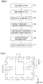
- is a flowchart illustrating a method of manufacturing a semiconductor device according to the first embodiment.
- FIG. 4
- is a schematic plan view showing the first step of the method of manufacturing a semiconductor device according to the first embodiment.
- FIG. 5
- is a schematic cross-sectional view showing the first step of the method of manufacturing a semiconductor device according to the first embodiment.
- FIG. 6
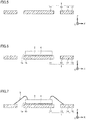
- is a schematic cross-sectional view showing the second step of the method of manufacturing a semiconductor device according to the first embodiment.
- FIG. 7
- is a schematic cross-sectional view showing the third step of the method of manufacturing a semiconductor device according to the first embodiment.
- FIG. 8
- is a schematic cross-sectional view showing the fourth step of the method of manufacturing a semiconductor device according to the first embodiment.
- FIG. 9
- is a schematic cross-sectional view showing the fifth step of the method of manufacturing a semiconductor device according to the first embodiment.
- FIG. 10
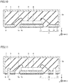
- is a schematic cross-sectional view showing the sixth step of the method of manufacturing a semiconductor device according to the first embodiment.
- FIG. 11
- is a schematic cross-sectional view showing the seventh step of the method of manufacturing a semiconductor device according to the first embodiment.
- FIG. 12
- is a schematic cross-sectional view of a semiconductor device in the first comparative example.
- FIG. 13
- is a schematic cross-sectional view showing the state in one step at some midpoint in a process of forming a semiconductor device in the second comparative example.
- FIG. 14
- is a flowchart illustrating a method of manufacturing a semiconductor device according to the second embodiment.
- FIG. 15
- is a schematic cross-sectional view of a semiconductor device according to the third embodiment.
- FIG. 16
- is a flowchart illustrating a method of manufacturing a semiconductor device according to the third embodiment.
- FIG. 17
- is a schematic cross-sectional view showing the seventh step subsequent to the step in
FIG. 10 of the method of manufacturing a semiconductor device according to the third embodiment. - FIG. 18
- is a schematic cross-sectional view showing the eighth step subsequent to the step in
FIG. 17 of the method of manufacturing a semiconductor device according to the third embodiment. - In the following, an Embodiment will be described with reference to the accompanying drawings.
- First, the configuration of a semiconductor device according to the present Embodiment will be hereinafter described with reference to
FIGS. 1 and 2. FIG. 1 is a schematic plan view of a semiconductor device according to the present embodiment.FIG. 2 is a schematic cross-sectional view of a portion of the semiconductor device according to the present embodiment, which is particularly taken along a line II-II inFIG. 1 . It is to be noted that some of regions such as an electrically conductive material shown inFIG. 2 are not shown inFIG. 1 . In each of the figures, an X direction, a Y direction and a Z direction are employed for convenience of explanation. Referring toFIGS. 1 and 2 , asemiconductor device 100 according to the present Embodiment mainly includes: alead frame 1; asemiconductor element 2; and amold material 3 as a plastic mold material. - Lead
frame 1 is formed as a base platform for theentire semiconductor device 100, provided as a flat plate-shaped member on which other members are placed, and preferably made of copper, for example. Alternatively,lead frame 1 may be made of an alloy of iron and nickel. Leadframe 1 includes, for example, onemain surface 1a on the upper side in the Z direction and the othermain surface 1b on the opposite side of onemain surface 1a, that is, on the lower side in the Z direction. As shown inFIG. 1 , onesemiconductor device 100 basically includes only asingle lead frame 1. - Furthermore,
lead frame 1 includes a die-attachportion 11, asignal terminal portion 12, and aground terminal portion 13. Die-attachportion 11 serves as a region on whichsemiconductor element 2 is placed so as to be joined thereto. Conversely,semiconductor element 2 is joined onto a part on onemain surface 1a oflead frame 1, particularly onto onemain surface 1a of die-attachportion 11. Die-attachportion 11 andsemiconductor element 2 are joined to each other with a joiningmaterial 4 interposed therebetween. It is preferable that joiningmaterial 4 is for example made of a solder material selected from the group consisting of: gold-tin alloy solder; lead-tin alloy solder; tin-silver-copper alloy solder; gold-germanium alloy solder; and gold-silicon alloy solder. Alternatively, joiningmaterial 4 may be any one selected from the group consisting of: sintered gold paste formed of gold powder particles each having a particle size less than 1 µm; sintered silver paste formed of silver powder particles each having a particle size equal to or greater than 1 nm and equal to or less than 10 nm, for example; and sintered copper paste formed of copper fine powder particles each having a surface subjected to a rust preventive process. Furthermore, joiningmaterial 4 may be made of an electrically conductive silver paste formed of silver powder particles each having a particle size equal to or greater than 1 µm and equal to or less than 100 µm, for example. - Signal
terminal portion 12 is electrically joined through athin metal wire 5 tosemiconductor element 2 that is joined to die-attachportion 11. Signalterminal portion 12 also allows electrical connection to the outside ofsemiconductor device 100. It is preferable thatthin metal wire 5 is any one selected from the group consisting of a gold wire, a silver wire and a copper wire, each of which has a cross section intersecting with the extending direction ofthin metal wire 5 and having a diameter of 10 µm or more and 50 µm or less. -
Ground terminal portion 13 is provided as a terminal connected to a ground potential (not shown). Basically, die-attachportion 11, signalterminal portion 12 andground terminal portion 13 are disposed so as to be arranged in the direction (for example, the X direction) along onemain surface 1a oflead frame 1, but the order of arrangement thereof is not particularly limited. Also, each of die-attachportion 11, signalterminal portion 12 andground terminal portion 13 may be provided in any number, and may be disposed at any position. However, as shown inFIGS. 1 and 2 , it is preferable that die-attachportion 11, signalterminal portion 12 andground terminal portion 13 are disposed so as to be arranged in this order, for example, in the X direction from the inside to the outside in a plan view. InFIG. 1 , die-attachportion 11, signalterminal portion 12 andground terminal portion 13 are arranged in this order from the inside to the outside in the X direction. In other words, signalterminal portion 12 is disposed on the outside of die-attachportion 11, andground terminal portion 13 is disposed on the outside ofsignal terminal portion 12. Also inFIG. 1 , die-attachportion 11 andground terminal portion 13 are arranged in this order from the inside to the outside in the Y direction. - It is to be noted that
ground terminal portion 13 is disposed on the outer circumferential portion ofmold material 3 in a plan view, irrespective of the above-described arrangement of die-attachportion 11, signalterminal portion 12 andground terminal portion 13. Specifically,ground terminal portion 13 is disposed on the outside of die-attachportion 11 and signalterminal portion 12 insemiconductor device 100 in a plan view. Furthermore,ground terminal portion 13 is disposed so as to surroundsignal terminal portion 12. Leadframe 1 has a schematic configuration as described above. -
Semiconductor element 2 is provided as a chip-shaped member made of any material selected from the group consisting of; silicon; silicon germanium; gallium arsenide; gallium nitride; and silicon carbide, for example. On the above-mentioned chip-shaped member ofsemiconductor element 2, a transistor, a circuit wiring interconnection and the like are integrated using the semiconductor wafer process technique. -
Mold material 3 is a member that covers onemain surface 1a oflead frame 1 and sealssemiconductor element 2. In other words,mold material 3 is disposed so as to cover and surroundlead frame 1,semiconductor element 2 andthin metal wire 5 from above in the Z direction. Also in other words, die-attachportion 11, signalterminal portion 12 andground terminal portion 13 are disposed directly below mold material 3 (below in the Z direction) so as to be arranged in the direction along onemain surface 1a oflead frame 1. - It is preferable that
mold material 3 is made of a material obtained by adding an inorganic filler such as spherical silica or pulverized silica to a thermosetting resin material such as an epoxy resin. By addition of an inorganic filler, the value of the coefficient of linear expansion ofmold material 3 and the value of the coefficient of linear expansion oflead frame 1 can be brought closer to each other, which can reduce the deformation and the internal stress that occur when an environmental temperature changes. - Lead
frame 1 is provided with agroove portion 6 between die-attachportion 11 andground terminal portion 13 that are adjacent to each other, and also betweensignal terminal portion 12 andground terminal portion 13 that are adjacent to each other. In other words,groove portion 6 is provided betweenground terminal portion 13 and one of die-attachportion 11 and signalterminal portion 12 that are adjacent to groundterminal portion 13.Groove portion 6 is provided as a region extending in the Z direction, which is provided by partially removinglead frame 1 so as to allowgroove portion 6 to pass throughlead frame 1 in the Z direction. As shown inFIG. 2 ,groove portion 6 passes throughlead frame 1 from the othermain surface 1b thereof so as to reach onemain surface 1a, and extends therefrom further upward in the Z direction. Thereby,groove portion 6 extends upward in the Z direction so as to reach the inside ofmold material 3 that is in contact with the upper side oflead frame 1 in the Z direction in an overlapping manner. - In addition,
semiconductor device 100 according to the present Embodiment includes an electricallyconductive material 7, acoating film 8, and anoxide film 9. Electricallyconductive material 7 is formed on the outside ofmold material 3 so as to cover at least a part ofmold material 3. InFIG. 2 , electricallyconductive material 7 is provided as a thin film formed so as to cover the upper surface ofmold material 3 that faces upward in the Z direction and to cover almost the entire surface of each of the side surfaces ofmold material 3 that face in the X direction (and in the Y direction, though not shown). - As described above, in
lead frame 1,ground terminal portion 13 is disposed on the outside of die-attachportion 11 and signalterminal portion 12 in a plan view, and also disposed on the outer circumferential portion ofmold material 3 in a plan view. Accordingly, the thin film of electricallyconductive material 7 that covers the outermost surface ofmold material 3 in the X direction and the Y direction is in contact with at least the side surface (the first side surface) ofground terminal portion 13 disposed on the outer circumferential portion ofmold material 3 in a plan view. In this case, the first side surface ofground terminal portion 13 faces in the X direction or the Y direction. Thus, the thin film of electricallyconductive material 7 is in contact with the surface ofground terminal portion 13 oflead frame 1 that extends in the Z direction corresponding to the thickness direction ofground terminal portion 13. For the purpose of allowing connection to electricallyconductive material 7,ground terminal portion 13 oflead frame 1 is disposed so as to include at least a part of the outermost circumference ofmold material 3 in a plan view. - It is preferable that electrically
conductive material 7 is formed of any one selected from the group consisting of: a thin metal film made of a copper alloy, a nickel alloy or the like; a thin film of an electrically conductive adhesive made of a silver paste or the like; and a plating film made of a copper alloy, a nickel alloy or the like. -
Coating film 8 is provided as a thin film formed on the othermain surface 1b of each of die-attachportion 11, signalterminal portion 12 andground terminal portion 13 inlead frame 1.Coating film 8 is basically formed for rust prevention oflead frame 1.Coating film 8 is any one selected from the group consisting of: a rust preventive film made of imidazole or the like; an electroless nickel plating film; an electroless nickel-gold plating film formed by layers of an electroless nickel plating film and an electroless gold plating film; and an electroless nickel-palladium-gold plating film formed by layers of an electroless nickel plating film, an electroless palladium plating film and an electroless gold plating film. Thereby, die-attachportion 11, signalterminal portion 12 andground terminal portion 13 inlead frame 1 can be protected from the othermain surface 1b side. -
Oxide film 9 is provided as a thin film formed on aside surface 1c (the second side surface) along which each of die-attachportion 11, signalterminal portion 12 andground terminal portion 13 oflead frame 1 adjoins to grooveportion 6. In other words,groove portion 6 oflead frame 1 hasside surface 1c adjoining to each of die-attachportion 11, signalterminal portion 12 andground terminal portion 13, and a fine oxide film is formed on thisside surface 1c. - Then, a method of manufacturing a semiconductor device according to the present Embodiment will be described with reference to the flowchart in
FIG. 3 and the schematic diagrams inFIGS. 4 to 11 andFIG. 2 . -
FIG. 3 is a flowchart illustrating the steps included in the method of manufacturing asemiconductor device 100 according to the present embodiment. Referring toFIG. 3 , a die-bonding step (S10), that is, the step of joiningsemiconductor element 2 to die-attachportion 11 oflead frame 1, is performed. It is to be noted that a lead frame is prepared before this step. -
FIG. 4 is a schematic plan view of a lead frame used in the method of manufacturing asemiconductor device 100 according to the present embodiment.FIG. 5 is a schematic cross-sectional view of a portion of the lead frame inFIG. 4 , which is taken along a line V-V inFIG. 4 . Thus, the arrangement of each of members inFIG. 4 is basically the same as the arrangement of each of the members in the semiconductor device according to the present Embodiment inFIG. 1 . Referring toFIGS. 4 and5 ,lead frame 1 including die-attachportion 11, signalterminal portion 12 andground terminal portion 13 is first prepared. In this case, basically, only asingle lead frame 1 is prepared for onesemiconductor device 100. - As described above, basically, die-attach
portion 11, signalterminal portion 12 andground terminal portion 13 are disposed so as to be arranged in the direction (for example, the X direction) along onemain surface 1a oflead frame 1. Also inFIG. 4 , die-attachportion 11, signalterminal portion 12 andground terminal portion 13 are arranged in this order from the inside to the outside in the X direction. In other words, signalterminal portion 12 is disposed on the outside of die-attachportion 11, andground terminal portion 13 is disposed on the outside ofsignal terminal portion 12. Also inFIG. 4 , die-attachportion 11 andground terminal portion 13 are arranged in this order from the inside to the outside in the Y direction. - In
lead frame 1, initially, die-attachportion 11 andground terminal portion 13 that are located adjacent to each other at a distance from each other in the Y direction inFIG. 4 are coupled to each other through atie bar 14 located therebetween. Also, signalterminal portion 12 andground terminal portion 13 that are located adjacent to each other at a distance from each other in the X direction inFIG. 4 are coupled to each other throughtie bar 14 located therebetween. In other words,lead frame 1 is initially (before the step of removing tie bar 14 (described below)) is formed as a flat plate-shaped member formed by integrating all of die-attachportion 11, signalterminal portion 12,ground terminal portion 13, and tiebar 14, as shown in the figure. Accordingly, for example, as compared with the case where thesemembers 11 to 14 are distinct members that are separate from each other,lead frame 1 in each step is readily handled, so thatsemiconductor device 100 can be efficiently fabricated. This is because all of thesemembers 11 to 14 are integrated with each other, so that the positional relation among these members is maintained. - Lead
frame 1 is made of an alloy of copper or iron and nickel as described above and formed in a flat plate shape. In the step of forminglead frame 1, for example, a copper material such as tough pitch copper or oxygen-free copper is subjected to cold rolling or the like, so that a metal member is formed in a flat plate shape having onemain surface 1a and the othermain surface 1b. Then, by wire electric discharge machining, press working and the like, die-attachportion 11, signalterminal portion 12,ground terminal portion 13 and the like are formed to be provided in any number and in any arrangement. The portion oftie bar 14 that is located betweenground terminal portion 13 and die-attachportion 11 or signalterminal portion 12 may be provided with a conveyance margin, a positioning hole, a pilot hole or the like used for handling oflead frame 1 in the steps and between the steps. -
FIG. 6 is a schematic cross-sectional view showing the state of the lead frame in the step subsequent toFIG. 5 . Referring toFIGS. 6 and3 ,semiconductor element 2 is joined onto onemain surface 1a of a portion allocated as die-attachportion 11 inlead frame 1 formed as shown inFIGS. 4 and5 (S10). When a solder material is used as joiningmaterial 4 in this case, an appropriate amount of string-shaped wire solder or plate-shaped ribbon solder is cut and used. - When the step in
FIG. 6 is performed using joiningmaterial 4 made of solder without using a flux in this case, the concentration of oxygen such as nitrogen around die-attachportion 11 is first lowered to about 200 ppm, and then heated to a temperature equal to or higher by about 20 °C and equal to or lower by about 30 °C than the melting point of solder. Thereby, the solder is melted, so that joiningmaterial 4 is sufficiently fitted between die-attachportion 11 oflead frame 1 andsemiconductor element 2. In this case, it is preferable to movesemiconductor element 2 in the horizontal direction, that is, in the direction along an X-Y plane. This allows joiningmaterial 4 to be more excellently fitted between die-attachportion 11 andsemiconductor element 2. Heating is ended when the solder of joiningmaterial 4 is sufficiently fitted. Then, joiningmaterial 4 is cooled to a temperature lower than the melting point of solder, so that joiningmaterial 4 is solidified. In this case, it is preferable that the cooling rate at the temperature around the melting point of solder is set to be equal to or higher than 4 °C and equal to or lower than 6 °C per second. This can reduce the difference between the solder solidifying timings, which is caused in response to the temperature difference between the outer circumference portion and the inside of joiningmaterial 4 that is located between die-attachportion 11 andsemiconductor element 2 in a plan view. Thereby, the state of joining by joiningmaterial 4 can be excellently improved. - When the step in
FIG. 6 is performed using joiningmaterial 4 made of solder also using a flux in this case, a flux in a liquid state or in a paste state may be supplied to string-shaped wire solder or plate-shaped ribbon solder. Alternatively, solder paste obtained by mixing powdered solder and a flux in advance may be used. In order to remove the residue of the flux adhering around the solder after the soldering step ends,lead frame 1 havingsemiconductor element 2 joined thereto is immersed in a flux cleaning solution. Then, the flux is dissolved. In this case, it is preferable thatlead frame 1 havingsemiconductor element 2 soldered thereto is shaken in the flux cleaning solution, the flux cleaning solution is caused to flow, or ultrasonic vibrations are applied to the flux cleaning solution. In this way, all of the flux residue can be readily removed. Also, it is preferable to warm the flux cleaning solution in advance in order to improve the solubility of the flux in the flux cleaning solution. - Also when the step in
FIG. 6 is performed using an electrically conductive adhesive as joiningmaterial 4 in this case, a dispensing scheme may be employed in which an electrically conductive adhesive filled in a syringe container is pushed out with air pressure, or a stamp scheme may be employed in which an electrically conductive adhesive spread over a transfer pan is transferred in a manner of a stamp. Thereby, a desired amount of electrically conductive adhesive is supplied to die-attachportion 11, on whichsemiconductor element 2 is then mounted, and then, the electrically conductive adhesive is pressed and spread. Then, the electrically conductive adhesive is heated by an oven and thereby thermally hardened, so thatlead frame 1 to whichsemiconductor element 2 is joined is formed. -
FIG. 7 is a schematic cross-sectional view showing the state of the lead frame in the step subsequent toFIG. 6 . Referring toFIGS. 7 and3 , a wire bonding step (S20) is performed, in whichsemiconductor element 2 joined to leadframe 1 as shown inFIG. 6 and signalterminal portion 12 are electrically joined throughthin metal wire 5.Thin metal wire 5 is provided as a thin wire made of aluminum, for example. In the wire bonding step,thin metal wire 5 is first placed through a cylindrical capillary tool. Then, the tip end ofthin metal wire 5 is heated and melted to form an initial ball. Thereby,thin metal wire 5 is ultrasonic heated and pressure bonded tosemiconductor element 2 and the like. -
FIG. 8 is a schematic cross-sectional view showing the state of the lead frame in the step subsequent toFIG. 7 . Referring toFIGS. 8 and3 , a plastic mold sealing step (S30) is performed, in whichmold material 3 serves to cover onemain surface 1a oflead frame 1 and sealsemiconductor element 2. Specifically, in the state where a metal mold having an inner wall surface to which a mold release material is thinly applied is heated in advance,lead frame 1 havingsemiconductor element 2 andthin metal wire 5 joined thereto as described above is placed inside the metal mold. Then, for example, by the transfer mold method,mold material 3 made of heated and softened plastic is pushed and introduced into the metal mold. Thereby, the inside of the metal mold is filled withmold material 3. Then,mold material 3 is hardened while maintaining the state where the metal mold is pressurized therein. Since the mold release material adheres to the inner wall surface of the metal mold, thehardened mold material 3 is readily removed without fixedly adhering to the metal mold. - By this step,
mold material 3 is supplied so as to be overlaid directly above die-attachportion 11, signalterminal portion 12 andground terminal portion 13. Thus, die-attachportion 11, signalterminal portion 12 andground terminal portion 13 inlead frame 1 are disposed directly belowmold material 3 so as to be arranged in the direction along onemain surface 1a. Also, each of the surfaces of die-attachportion 11, signalterminal portion 12 andground terminal portion 13 that are located on themain surface 1a side is covered withmold material 3 so as to be sealed. - As described above,
ground terminal portion 13 is disposed on the outside of die-attachportion 11 and signalterminal portion 12 in a plan view. In the step inFIG. 8 ,ground terminal portion 13 is disposed on the outer circumferential portion ofmold material 3 in a plan view. -
FIG. 9 is a schematic cross-sectional view showing the state of the lead frame in the step subsequent toFIG. 8 . Referring toFIGS. 9 and3 , a surface treatment coating formation step (S40) is performed, in whichcoating film 8 is formed on the othermain surface 1b on the opposite side of onemain surface 1a of each of die-attachportion 11, signalterminal portion 12 andground terminal portion 13. In this step,coating film 8 is formed entirely over the othermain surface 1b oflead frame 1, so that coatingfilm 8 is formed also on the othermain surface 1b of the portion corresponding to tiebar 14, for example.Coating film 8 may be formed, for example, due to adhesion of a rust preventive film made of imidazole as a result of immersion in a liquid phase of a rust preventive material such as imidazole. - Alternatively, when a plating film is formed as
coating film 8, the following process is performed. First,lead frame 1 includingsemiconductor element 2 and the like sealing bymold material 3 is washed by an acid cleaning solution. This leads to removal of the oxide film on the othermain surface 1b of the portion particularly corresponding to each of die-attachportion 11, signalterminal portion 12,ground terminal portion 13, and tiebar 14 inlead frame 1. Then,lead frame 1 is immersed in an electroless plating solution, so that an electroless plating film is deposited on the othermain surface 1b. When an electroless nickel gold plating film is formed in this step, it is preferable that the layered films forming this electroless nickel gold plating film include: an electroless nickel plating film having a thickness of 5 µm or more; and an electroless gold plating film having a thickness of 0.05 µm or more. This can suppress occurrence of defects that may be caused when the completedsemiconductor device 100 is surface-mounted on high frequency equipment. -
FIG. 10 is a schematic cross-sectional view showing the state of the lead frame in the step subsequent toFIG. 9 . Referring toFIGS. 10 and3 , an electrically conductive material formation step (S50) is performed, in which electricallyconductive material 7 is formed to cover at least a part ofmold material 3 and to be in contact with at least the side surface (the first side surface) ofground terminal portion 13. In this case, a mold release material on the inner wall surface of the metal mold used in the sealing step adheres to the surface ofmold material 3. Accordingly, it is preferable that a thin film of electricallyconductive material 7 is formed after the adhering mold release material is sufficiently removed. It is preferable that electricallyconductive material 7 is formed after the othermain surface 1b oflead frame 1 is covered in advance with a mask member. This can suppress adhesion of electricallyconductive material 7 to the othermain surface 1b. - When the thin film of electrically
conductive material 7 is made of a thin metal film of a copper alloy, a nickel alloy or the like, it is preferable that electricallyconductive material 7 is formed by a processing method selected from the group consisting of: vapor deposition; sputtering; electroplating; and electroless plating. Alternatively, when the thin film of electricallyconductive material 7 is formed of a thin film of an electrically conductive adhesive such as a silver paste, it is preferable to form this thin film of electricallyconductive material 7 by using an oven or the like to thermally harden electricallyconductive material 7 applied onto the surface and the like ofmold material 3 by any one method selected from the group consisting of: screen printing; spraying; and electro-deposition coating. In this case, when a pressure-sensitive adhesive tape is affixed in advance as a mask member onto the othermain surface 1b oflead frame 1, the mask member can be readily removed after a silver paste is applied. This can suppress occurrence of defects that may be caused when the completedsemiconductor device 100 is surface-mounted on high frequency equipment. -
FIG. 11 is a schematic cross-sectional view showing the state of the lead frame in the step subsequent toFIG. 10 . Referring toFIGS. 11 and3 , a groove portion providing step (S60) is performed, in whichgroove portion 6 is provided by partially removinglead frame 1 so as to allowgroove portion 6 to pass throughlead frame 1 such thatgroove portion 6 is provided between die-attachportion 11 andground terminal portion 13 that are adjacent to each other and betweensignal terminal portion 12 andground terminal portion 13 that are adjacent to each other. Specifically, the portion oftie bar 14 inlead frame 1 and the portion ofcoating film 8 that overlaps therewith are removed to provide a groove portion so as to pass throughlead frame 1 from the othermain surface 1b to onemain surface 1a. Thereby, die-attachportion 11 andground terminal portion 13 that are spaced apart from each other are separated from each other whilesignal terminal portion 12 andground terminal portion 13 that are spaced apart from each other are separated from each other. Furthermore,groove portion 6 is provided so as to reach the inside ofmold material 3 that is in contact with the portion oftie bar 14 oflead frame 1 in the Z direction in an overlapping manner. In other words,groove portion 6 is provided by partially removingmold material 3 in a region overlapping with the removed portion oflead frame 1 in a plan view, as shown inFIG. 11 . Also in other words,groove portion 6 extends fromlead frame 1 to the inside ofmold material 3 in the Z direction. - As the means for providing
groove portion 6, cutting processing such as blade saw processing using a disc-shaped saw and router processing using a cylindrical drill may be used, or laser beam machining using a laser beam may be used. - Again referring to
FIGS. 2 and3 , an oxide film formation step (S70) is performed, in whichoxide film 9 is formed onside surface 1c (the second side surface) along which die-attachportion 11, signalterminal portion 12 andground terminal portion 13 adjoin to grooveportion 6. Specifically, aftergroove portion 6 is provided,lead frame 1 is heat-treated in an oven with atmospheric air. Thereby, afine oxide film 9 is formed on the second side surface along which each of die-attachportion 11, signalterminal portion 12 andground terminal portion 13 oflead frame 1 adjoins to grooveportion 6. - Although not shown,
semiconductor device 100 formed as described above is surface-mounted on high-frequency applicable equipment so as to be used. - In the following, the functions and effects of the present Embodiment will be described with reference to a comparative example.
-
FIG. 12 is a schematic cross-sectional view of a semiconductor device according to the first comparative example. Referring toFIG. 12 , for asemiconductor device 901 according to the first comparative example, the same components as those insemiconductor device 100 according to the present Embodiment will be designated by the same reference characters, and the description thereof will not be repeated. As shown inFIG. 12 , in the first comparative example,lead frame 1 includes die-attachportion 11 and signalterminal portion 12, and theentire semiconductor element 2 joined onto die-attachportion 11 and a part ofsignal terminal portion 12 are covered and sealed bymold material 3. A part ofsignal terminal portion 12 extends so as to protrude from anoutermost surface 3a ofmold material 3 to the outside in a plan view. In addition,outermost surface 3a ofmold material 3 located abovesignal terminal portion 12 in the Z direction is covered by anupper metal case 71 corresponding to electricallyconductive material 7 ofsemiconductor device 100. Also,outermost surface 3a ofmold material 3 located belowsignal terminal portion 12 in the Z direction is covered by alower metal case 72 corresponding to electricallyconductive material 7 ofsemiconductor device 100. - In
such semiconductor device 901, signalterminal portion 12 protrudes frommold material 3 to the outside in a plan view, so that the area occupied by the entire device is increased. -
FIG. 13 is a schematic cross-sectional view showing the state in one step at some midpoint in a process of forming a semiconductor device in the second comparative example. Referring toFIG. 13 , for asemiconductor device 902 according to the second comparative example, the same components as those insemiconductor device 100 according to the present Embodiment will be designated by the same reference characters, and the description thereof will not be repeated. As shown inFIG. 13 , in the second comparative example, two lead frames including afirst lead frame 10 and asecond lead frame 19 are disposed as lead frames. These two lead frames are overlapped with each other in the Z direction in the step of manufacturingsemiconductor device 902. - Specifically, in the manufacturing step,
first lead frame 10 includes asignal terminal portion 12 and aninsertion portion 15 that is located on the outside ofsignal terminal portion 12 in the X direction. Signalterminal portion 12 andinsertion portion 15 are spaced apart from each other in the X direction. Signalterminal portion 12 andinsertion portion 15 each extend upward in the Z direction from the base portion that includes: amain surface 1d on the upper side offirst lead frame 10 in the Z direction; and the othermain surface 1b on the opposite side ofmain surface 1d. Furthermore, the othermain surface 1b is formed as a main surface of the lowermost portion of the two entire lead frames in the Z direction. - On the other hand,
second lead frame 19 includes die-attachportion 11 andground terminal portion 13 that is located on the outside of die-attachportion 11 in the X direction. Die-attachportion 11 andground terminal portion 13 are spaced apart from each other in the X direction. Die-attachportion 11 is disposed in the center portion ofsecond lead frame 19. Also, the upper main surface of die-attachportion 11 is formed as onemain surface 1a corresponding to the uppermost main surface of the two entire lead frames in the Z direction. Most part ofground terminal portion 13 is formed as a portion located on the outside of die-attachportion 11 and including: amain surface 1e on the upper side in the Z direction; and amain surface 1f on the opposite side ofmain surface 1e and on the lower side in the Z direction. In this case, a portion ofground terminal portion 13 that is located closest to die-attachportion 11 is slightly bent so as to extend in the Z direction.Ground terminal portion 13 is provided with anopening 16 that passes throughground terminal portion 13 in the Z direction frommain surface 1e on the upper side to main surface If on the lower side. -
Insertion portion 15 offirst lead frame 10 is inserted into opening 16 ofsecond lead frame 19, thereby forming a fittedregion 17 in which two lead frames are fitted to each other. The entirety of die-attachportion 11, signalterminal portion 12 andsemiconductor element 2, and a part of ground terminal portion 13 (a portion closest to die-attachportion 11 that is bent so as to extend in the Z direction) are sealed bymold material 3 while most part ofground terminal portion 13 andopening 16 are disposed on the outside ofmold material 3. - After two lead frames are assembled by fitted
region 17 as described above, the portion below a dashedline 18 in the Z direction is removed, thereby formingsemiconductor device 902. In thissemiconductor device 902, each ofsignal terminal portion 12 andground terminal portion 13 is exposed from the lowermost surface ofmold material 3 after the above-mentioned removal. This can eliminate the problem that the entire area is increased by a lead frame as insemiconductor device 901. However,semiconductor device 902 has a configuration in which two lead frames are assembled, thereby complicating the step of assembling these two lead frames. Furthermore, fittedregion 17 and the like are eventually removed. Thus, only a small portion of the produced lead frames eventually remains insemiconductor device 902, which leads to a problem that the utilization efficiency of the lead frame materials for a product is deteriorated. - Thus, in
semiconductor device 100 according to the present embodiment, die-attachportion 11, signalterminal portion 12 andground terminal portion 13 are first disposed directly belowmold material 3 so as to be arranged in the direction along onemain surface 1a oflead frame 1. In other words, signalterminal portion 12 does not protrude frommold material 3 in a plan view, unlikesemiconductor device 901. Accordingly, the area occupied bysemiconductor device 100 can be equal to the plane area ofmold material 3, and can be smaller than that in the configuration ofsemiconductor device 901. Thus, also whensemiconductor device 100 is surface-mounted on high-frequency applicable equipment, the area occupied by thissemiconductor device 100 can be reduced. - Furthermore,
semiconductor device 100 is formed only ofsingle lead frame 1. This eliminates the need to employ the manufacturing method of assembling two lead frames as insemiconductor device 902, so that the manufacturing step can be simplified. Also, fittedregion 17 and a region to be removed are eliminated, so that the utilization efficiency of the lead-frame forming material for a product can be improved. - In addition, in
semiconductor device 100 according to the present embodiment,groove portion 6 is provided between die-attachportion 11 andground terminal portion 13 so that die-attachportion 11 andground terminal portion 13 are electrically insulated from each other, and also,groove portion 6 is provided betweensignal terminal portion 12 andground terminal portion 13 so thatsignal terminal portion 12 andground terminal portion 13 are electrically insulated from each other. Furthermore,ground terminal portion 13 is connected to a ground potential, and disposed on the outer circumferential portion ofmold material 3 in a plan view. Thereby,ground terminal portion 13 is readily connected to the ground potential, and signalterminal portion 12 can block an input and an output of electromagnetic waves to the outside. This is becauseground terminal portion 13 serves to block the input of electromagnetic waves to signalterminal portion 12 and the output of electromagnetic waves fromsignal terminal portion 12 while maintaining insulation fromsignal terminal portion 12. - In order to block the input/output of electromagnetic waves as mentioned above, in
lead frame 1 according to the present embodiment, it is preferable that signalterminal portion 12 is disposed on the outside of die-attachportion 11 whileground terminal portion 13 is disposed on the outside ofsignal terminal portion 12. Thereby,ground terminal portion 13 can surround signalterminal portion 12 from the outside in a plan view, thereby enhancing the effect byground terminal portion 13 of blocking the input of electromagnetic waves to signalterminal portion 12 and the output of electromagnetic waves fromsignal terminal portion 12. - Furthermore, electrically
conductive material 7 is formed so as to be in contact with at least the first side surface ofground terminal portion 13. Since electricallyconductive material 7 is formed so as to cover at least a part of mold material 3 (basically, the almost entirety of the uppermost surface and the side surface), electricallyconductive material 7 andground terminal portion 13 are brought into contact with each other and set to be at the same potential. Thereby, an electromagnetic shield structure is formed byground terminal portion 13 and electricallyconductive material 7 that covers the outermost surface ofmold material 3. Thus,ground terminal portion 13 can enhance the blocking effect forsignal terminal portion 12 surrounded by thisground terminal portion 13. -
Oxide film 9 is formed on the second side surface of the side surfaces ofgroove portion 6, which is in contact with die-attachportion 11, signalterminal portion 12 andground terminal portion 13. Thereby, it becomes possible to prevent wetting and spreading of the mounting solder from occurring on the second side surface ofgroove portion 6 whensemiconductor device 100 is surface-mounted on high-frequency applicable equipment. This is becauseoxide film 9 is less likely to be wet with solder. Accordingly, it becomes possible to decrease the possibility that die-attachportion 11, signalterminal portion 12 andground terminal portion 13 inlead frame 1 are electrically short-circuited. - Since the semiconductor device according to the present Embodiment has basically the same configuration as that of
semiconductor device 100 according to the first embodiment, the detailed explanation thereof will not be repeated. The present Embodiment is different partially in the manufacturing method from the first embodiment. In the following, the method of manufacturing a semiconductor device in the present Embodiment will be described with reference toFIG. 14 . -
FIG. 14 is a flowchart illustrating the steps included in the method of manufacturing asemiconductor device 100 according to the present embodiment. Referring toFIG. 14 , in the present embodiment, the order of the electrically conductive material formation step (S50) and the groove portion providing step (S60) in the manufacturing method in the first Embodiment inFIG. 3 is reversed. Specifically, in the present embodiment, the step of forming electrically conductive material 7 (seeFIG. 10 ) is performed after the step of providing groove portion 6 (seeFIG. 11 ). - The manufacturing method according to the present Embodiment is basically the same as the manufacturing method according to the first Embodiment except for the above-described points, and therefore, the description thereof will not be hereinafter repeated.
- Although not described above, there is an additional step of drying moisture adhering to
semiconductor device 100 after a plating film made of a copper alloy, a nickel alloy or the like is processed as electricallyconductive material 7. Thus, for example, when a plating film is formed as electricallyconductive material 7 aftergroove portion 6 is provided,oxide film 9 can be formed on the second side surface ofgroove portion 6 in the step of drying moisture. Accordingly, in the present embodiment, the oxide film formation step (S70) can be substantially eliminated. - Since the semiconductor device according to the present Embodiment has basically the same configuration as that of
semiconductor device 100 according to the first embodiment, the same components as those insemiconductor device 100 will be hereinafter designated by the same reference characters, and the description thereof will not be repeated. It is to be noted that the present Embodiment is different partially in configuration from the first embodiment. In the following, structural differences between the semiconductor device in the present Embodiment andsemiconductor device 100 will be described with reference toFIG. 15 . -
FIG. 15 is a schematic cross-sectional view of a semiconductor device according to the third embodiment. Referring toFIG. 15 , asemiconductor device 200 according to the present Embodiment is different in configuration ofgroove portion 6 fromsemiconductor device 100. Specifically,groove portion 6 insemiconductor device 200 is approximately barrel-shaped in such a manner that a width W1 in the X direction (and the Y direction) in the center portion in the Z direction is greater in a cross-sectional view than a width W2 in the X direction (and the Y direction) at each of the upper end portion and the lower end portion in the Z direction. - In other words,
groove portion 6 insemiconductor device 200 includes: afirst region 61 in the center portion in the Z direction in a cross-sectional view; and asecond region 62 excluding the first region, that is, located at the upper end portion and the lower end portion in the Z direction in a cross-sectional view.Groove portion 6 is provided such that itssecond side surface 1c bulges outward in such a manner that width W1 in the X direction and the Y direction along onemain surface 1a infirst region 61 is greater than width W2 in the X direction and the Y direction along onemain surface 1a insecond region 62. As a result,side surface 1c along which signalterminal portion 12 andground terminal portion 13 adjoin to grooveportion 6 is curved so as to bulge as described above, as shown inFIG. 15 . Sinceside surface 1c ofgroove portion 6 is curved,oxide film 9 formed thereon is similarly curved in a barrel shape. It is preferable that width W1 is 1.1 times or more and 1.3 times or less, for example, 1.2 times, as large as width W2. - Furthermore,
FIG. 15 shows an example in whichgroove portion 6 betweensignal terminal portion 12 andground terminal portion 13 has a barrel shape. In the present embodiment,groove portion 6 between die-attachportion 11 andground terminal portion 13 may also be similarly formed to have a barrel shape. - The method of manufacturing a
semiconductor device 200 according to the present Embodiment is basically the same as the method of manufacturing asemiconductor device 100 according to the first embodiment, but is slightly different therefrom in the process for providing a barrel-shapedgroove portion 6 as described above. The method of manufacturing a semiconductor device according to the present Embodiment will be described below with reference to the flowchart inFIG. 16 and the schematic diagrams inFIGS. 17 and 18 . -
FIG. 16 is a flowchart illustrating the steps included in the method of manufacturing asemiconductor device 200 according to the present embodiment. Referring toFIG. 16 , in the method ofmanufacturing semiconductor device 200 according to the present embodiment, the steps up to the steps (S10) to (S50) are performed in the same manner as in the first embodiment, and therefore, the description thereof will not be hereinafter repeated. -
FIG. 17 is a schematic cross-sectional view showing the state of the lead frame in the step subsequent to the step (S50) in the first embodiment, that is, the step of forming electricallyconductive material 7 shown inFIG. 10 . Referring toFIGS. 17 and16 , a surface treatment coating removal step (S60A) is performed, in whichcoating film 8 as a surface treatment coating formed in the step (S40) is partially removed. Specifically, the surface treatment coating removal step (S60A) is performed as a part of the step of providinggroove portion 6, and performed to removecoating film 8 formed so as to overlap withtie bar 14 on the region in whichgroove portion 6 is to be provided, that is, on the othermain surface 1b oftie bar 14. - In order to allow a coating film removed
region 81 havingcoating film 8 removed therefrom to be formed directly belowtie bar 14 as shown inFIG. 17 , for example, the following process is performed. A mask member (not shown) is attached to the lower surface ofcoating film 8 in the Z direction that is formed in the region other than the region directly belowtie bar 14. In this state,lead frame 1 is introduced and immersed in the first chemical solution. It is preferable that the first chemical solution used herein is a chemical solution that can readily dissolvecoating film 8 but cannot readily dissolvelead frame 1. This leads to dissolution and removal ofcoating film 8 formed ontie bar 14 that is exposed because a mask member is not attached thereto. Consequently, the state shown inFIG. 17 is achieved. - Alternatively, coating film removed
region 81 may be formed by the following method. For example, only a portion ofcoating film 8 that is formed ontie bar 14 is subjected to laser beam machining, thereby removing only this portion ofcoating film 8, so that coating film removedregion 81 is provided. -
FIG. 18 is a schematic cross-sectional view showing the state of the lead frame in the step subsequent toFIG. 17 . Referring toFIGS. 18 and16 ,lead frame 1 is introduced and immersed in the second chemical solution in the state where coating film removedregion 81 is provided directly belowtie bar 14. It is preferable that the second chemical solution used herein is a chemical solution that cannot readily dissolvecoating film 8 but can readily dissolvelead frame 1. Thereby, a portion oflead frame 1 that overlaps with coating film removedregion 81 is removed without removingcoating film 8. - In this case, not only in the portion of
tie bar 14 that overlaps with coating film removedregion 81 but also particularly in the center portion oflead frame 1 in the Z direction, signalterminal portion 12 andground terminal portion 13 located therearound are partially dissolved. In other words, removal is done such that the width of the region from which leadframe 1 includingtie bar 14 has been removed is greater than the width of the region from whichcoating film 8 has been removed. The width used herein means a width in the direction along onemain surface 1a oflead frame 1 along the X direction (or the Y direction) inFIG. 18 . Thereby, the region from which leadframe 1 has been removed is provided asgroove portion 6 including:first region 61 in whichsecond side surface 1c partially bulges outward; andsecond region 62 other than first region 61 (S60B). The combination of the above-described steps (S60A) and (S60B) corresponds to the groove portion providing step (S60) in the first embodiment. - Since the subsequent step (S70) is performed in the same manner as in the first embodiment, the description thereof will not be hereinafter repeated.
- By providing barrel-shaped
groove portion 6 includingfirst region 61 andsecond region 62 as in the present embodiment, it becomes possible to increase the distance between die-attachportion 11 and signalterminal portion 12 adjacent to each other inlead frame 1 and the distance betweensignal terminal portion 12 andground terminal portion 13 adjacent to each other inlead frame 1. This is because the width ofgroove portion 6 is increased by the amount of outward bulging offirst region 61. Thus, it becomes possible to more reliably suppress wetting and spreading of surface mounting solder from occurring inside barrel-shapedgroove portion 6 whensemiconductor device 200 is surface-mounted on high-frequency applicable equipment. - Also in the present embodiment, the order of the steps (S50) and (S60) may be reversed as in the second embodiment. In this case, the step (S60) in
FIG. 14 is replaced with the step (S60B) inFIG. 16 , and the step (S60A) inFIG. 16 is inserted between the step (S40) and the step (S60B). - The characteristics described in (each of the examples included in) each of the embodiments as described above may be combined as appropriate within the range where technical inconsistency does not occur.
- It should be understood that the embodiments disclosed herein are illustrative and non-restrictive in every respect. The scope of the present invention is defined by the terms of the claims, rather than the description above, and is intended to include any modifications within the meaning and scope equivalent to the terms of the claims.
-
- 1
- lead frame
- 1a
- one main surface
- 1b
- the other main surface
- 1c
- side surface
- 1d, 1e
- upper main surface
- 1f
- lower main surface
- 2
- semiconductor element
- 3
- mold material
- 3a
- outermost surface
- 4
- joining material
- 5
- thin metal wire
- 6
- groove portion
- 7
- electrically conductive material
- 8
- coating film
- 9
- oxide film
- 10
- first lead frame
- 11
- die-attach portion
- 12
- signal terminal portion
- 13
- ground terminal portion
- 14
- tie bar
- 15
- insertion portion
- 16
- opening
- 17
- fitted region
- 18
- dashed line
- 19
- second lead frame
- 61
- first region
- 62
- second region
- 71
- upper metal case
- 72
- lower metal case
- 81
- coating film removed region
- 100, 200, 901, 902
- semiconductor device.
Claims (11)
- A semiconductor device comprising:- a single lead frame;- a semiconductor element that is joined onto one main surface of the lead frame; and- a mold material that covers the one main surface of the lead frame and seals the semiconductor element, whereinthe lead frame includes
a die-attach portion to which the semiconductor element is joined,
a signal terminal portion electrically joined to the semiconductor element through a thin metal wire, and
a ground terminal portion connected to a ground potential and disposed on an outer circumferential portion of the mold material in a plan view,
the die-attach portion, the signal terminal portion and the ground terminal portion are disposed directly below the mold material so as to be arranged in a direction along the one main surface, and
the lead frame is provided with a groove portion by partially removing the lead frame so as to allow the groove portion to pass through the lead frame, the groove portion being provided between the die-attach portion and the ground terminal portion that are adjacent to each other and between the signal terminal portion and the ground terminal portion that are adjacent to each other. - The semiconductor device according to claim 1, wherein- the signal terminal portion is disposed on an outside of the die-attach portion, and- the ground terminal portion is disposed on an outside of the signal terminal portion.
- The semiconductor device according to claim 1 or 2, wherein the groove portion is provided so as to reach an inside of the mold material that is in contact with the lead frame in an overlapping manner.
- The semiconductor device according to any one of claims 1 to 3, further comprising:- an electrically conductive material that covers at least a part of the mold material and that is in contact with at least a first side surface of the ground terminal portion;- a coating film formed on the other main surface on an opposite side of the one main surface of each of the die-attach portion, the signal terminal portion and the ground terminal portion; and- an oxide film formed on a second side surface of the groove portion,the die-attach portion, the signal terminal portion and the ground terminal portion being located to adjoin to the groove portion along the second side surface.
- The semiconductor device according to claim 4, wherein
the groove portion includes a first region and a second region other than the first region, and
the second side surface of the groove portion bulges outward such that the first region is greater in width in a direction along the one main surface than the second region. - A method of manufacturing a semiconductor device, the method comprising:preparing a single lead frame including a die-attach portion, a signal terminal portion, and a ground terminal portion that is connected to a ground potential;joining a semiconductor element to the die-attach portion of the lead frame;electrically joining the semiconductor element and the signal terminal portion to each other through a thin metal wire;by a mold material, covering one main surface of the lead frame and sealing the semiconductor element; andproviding a groove portion by partially removing the lead frame so as to allow the groove portion to pass through the lead frame, the groove portion being provided between the die-attach portion and the ground terminal portion that are adjacent to each other and between the signal terminal portion and the ground terminal portion that are adjacent to each other, whereinin the sealing, the mold material is supplied so as to be overlaid directly above the die-attach portion, the signal terminal portion and the ground terminal portion, andin the sealing, the ground terminal portion is disposed on an outer circumferential portion of the mold material in a plan view.
- The method of manufacturing a semiconductor device according to claim 6, wherein- in the preparing a single lead frame,the signal terminal portion is formed on an outside of the die-attach portion, and the ground terminal portion is formed on an outside of the signal terminal portion.
- The method of manufacturing a semiconductor device according to claim 6 or 7, wherein- in the providing a groove portion, the groove portion is provided so as to reach an inside of the mold material that is in contact with the lead frame in an overlapping manner.
- The method of manufacturing a semiconductor device according to any one of claims 6 to 8, further comprising:- forming an electrically conductive material that covers at least a part of the mold material and that is in contact with at least a first side surface of the ground terminal portion;- forming a coating film on the other main surface on an opposite side of the one main surface of each of the die-attach portion, the signal terminal portion and the ground terminal portion; andforming an oxide film on a second side surface of the groove portion,
the die-attach portion, the signal terminal portion and the ground terminal portion being located to adjoin to the groove portion along the second side surface. - The method of manufacturing a semiconductor device according to claim 9, wherein the forming an electrically conductive material is performed after the providing a groove portion.
- The method of manufacturing a semiconductor device according to claim 9 or 10, wherein- the providing a groove portion includesremoving the coating film formed on the other main surface in a region in which the groove portion is to be provided, andby immersing the lead frame in a chemical solution in a state where the coating film is removed, removing a portion of the lead frame that overlaps with a region from which the coating film is removed, and by the removing a portion of the lead frame, the lead frame is partially removed such that a width of a region from which the lead frame is removed is greater than a width of the region from which the coating film is removed, to provide the groove portion in which the second side surface partially bulges outward.
Applications Claiming Priority (2)
| Application Number | Priority Date | Filing Date | Title |
|---|---|---|---|
| JP2017093199 | 2017-05-09 | ||
| PCT/JP2018/016091 WO2018207583A1 (en) | 2017-05-09 | 2018-04-19 | Semiconductor device and method for manufacturing same |
Publications (2)
| Publication Number | Publication Date |
|---|---|
| EP3624180A1 true EP3624180A1 (en) | 2020-03-18 |
| EP3624180A4 EP3624180A4 (en) | 2020-04-01 |
Family
ID=64104546
Family Applications (1)
| Application Number | Title | Priority Date | Filing Date |
|---|---|---|---|
| EP18797540.4A Withdrawn EP3624180A4 (en) | 2017-05-09 | 2018-04-19 | SEMICONDUCTOR DEVICE AND MANUFACTURING METHOD THEREOF |
Country Status (4)
| Country | Link |
|---|---|
| US (1) | US11114386B2 (en) |
| EP (1) | EP3624180A4 (en) |
| JP (1) | JP6723448B2 (en) |
| WO (1) | WO2018207583A1 (en) |
Families Citing this family (6)
| Publication number | Priority date | Publication date | Assignee | Title |
|---|---|---|---|---|
| CN112242373A (en) * | 2019-07-19 | 2021-01-19 | 上海凯虹科技电子有限公司 | Lead frame and packaging mold |
| JP2022133486A (en) * | 2019-07-30 | 2022-09-14 | 株式会社デンソー | Semiconductor package and semiconductor device |
| JP7506543B2 (en) * | 2020-07-07 | 2024-06-26 | 株式会社巴川コーポレーション | Element protection structure and manufacturing method thereof |
| JP7482072B2 (en) * | 2021-03-22 | 2024-05-13 | 株式会社東芝 | Semiconductor Device |
| JPWO2022224811A1 (en) * | 2021-04-19 | 2022-10-27 | ||
| US20220384362A1 (en) * | 2021-05-31 | 2022-12-01 | Ubotic Company Limited | Faraday cage plastic cavity package with pre-molded cavity leadframe |
Family Cites Families (16)
| Publication number | Priority date | Publication date | Assignee | Title |
|---|---|---|---|---|
| TW543172B (en) | 2001-04-13 | 2003-07-21 | Yamaha Corp | Semiconductor device and package, and method of manufacture therefor |
| JP3909575B2 (en) * | 2002-01-22 | 2007-04-25 | ヤマハ株式会社 | Semiconductor device and manufacturing method thereof |
| JP4034073B2 (en) * | 2001-05-11 | 2008-01-16 | 株式会社ルネサステクノロジ | Manufacturing method of semiconductor device |
| US6510976B2 (en) * | 2001-05-18 | 2003-01-28 | Advanpack Solutions Pte. Ltd. | Method for forming a flip chip semiconductor package |
| JP2006319014A (en) | 2005-05-11 | 2006-11-24 | Sharp Corp | Electronic components for high frequency signal reception |
| JP2008078323A (en) * | 2006-09-20 | 2008-04-03 | Yamaha Corp | Surface mount semiconductor package |
| JP4531073B2 (en) * | 2007-03-20 | 2010-08-25 | 三洋電機株式会社 | Semiconductor device |
| US8120150B2 (en) * | 2007-09-18 | 2012-02-21 | Stats Chippac Ltd. | Integrated circuit package system with dual connectivity |
| US20120181676A1 (en) * | 2008-04-04 | 2012-07-19 | GEM Service, Inc. | Power semiconductor device packaging |
| JP2010040854A (en) | 2008-08-06 | 2010-02-18 | Nec Electronics Corp | Ic molded package, and method of manufacturing the same |
| US8969136B2 (en) * | 2011-03-25 | 2015-03-03 | Stats Chippac Ltd. | Integrated circuit packaging system for electromagnetic interference shielding and method of manufacture thereof |
| US9717146B2 (en) * | 2012-05-22 | 2017-07-25 | Intersil Americas LLC | Circuit module such as a high-density lead frame array (HDA) power module, and method of making same |
| JP5802695B2 (en) * | 2013-03-19 | 2015-10-28 | 株式会社東芝 | Semiconductor device and method for manufacturing semiconductor device |
| US10396039B2 (en) * | 2014-12-09 | 2019-08-27 | Mitsubishi Electric Corporation | Semiconductor package |
| JP6555927B2 (en) * | 2015-05-18 | 2019-08-07 | 大口マテリアル株式会社 | Semiconductor device mounting lead frame and semiconductor device manufacturing method |
| JP6149072B2 (en) * | 2015-07-07 | 2017-06-14 | アオイ電子株式会社 | Semiconductor device and manufacturing method thereof |
-
2018
- 2018-04-19 JP JP2019517540A patent/JP6723448B2/en active Active
- 2018-04-19 US US16/491,620 patent/US11114386B2/en active Active
- 2018-04-19 WO PCT/JP2018/016091 patent/WO2018207583A1/en not_active Ceased
- 2018-04-19 EP EP18797540.4A patent/EP3624180A4/en not_active Withdrawn
Also Published As
| Publication number | Publication date |
|---|---|
| WO2018207583A1 (en) | 2018-11-15 |
| JP6723448B2 (en) | 2020-07-15 |
| US20200058598A1 (en) | 2020-02-20 |
| EP3624180A4 (en) | 2020-04-01 |
| JPWO2018207583A1 (en) | 2019-12-12 |
| US11114386B2 (en) | 2021-09-07 |
Similar Documents
| Publication | Publication Date | Title |
|---|---|---|
| US11114386B2 (en) | Semiconductor device and method of manufacturing the same | |
| CN100527614C (en) | Method for the hermetic encapsulation of a component | |
| US7268426B2 (en) | High-frequency chip packages | |
| US9620471B2 (en) | Power semiconductor package with conductive clips | |
| US8232144B2 (en) | Non-pull back pad package with an additional solder standoff | |
| CN101322242B (en) | Hermetic sealing cap, electronic device housing package, and method of manufacturing hermetic sealing cap | |
| CN205282448U (en) | Surface mounting type semiconductor device | |
| CN102646609B (en) | Semiconductor device, manufacturing method of semiconductor device, and power source device | |
| US7507605B2 (en) | Low cost lead-free preplated leadframe having improved adhesion and solderability | |
| JP2000040775A (en) | Semiconductor device and manufacturing method thereof | |
| US20110038132A1 (en) | Microstructure Apparatus, Manufacturing Method Thereof, and Sealing Substrate | |
| US8179686B2 (en) | Mounted structural body and method of manufacturing the same | |
| JP5300470B2 (en) | Semiconductor package and method for forming the same | |
| JP2008235531A (en) | Hermetically sealed package and connection structure | |
| CN112786469B (en) | Bulk diffusion welding and electronic device produced by bulk diffusion welding | |
| JP2001110845A (en) | Flip chip mounting structure | |
| US20040021219A1 (en) | Method of mounting integrated circuit die in a package using a solder preform having isolatable portions | |
| TWI918503B (en) | Semiconductor device with compartment shield formed from metal bars and manufacturing method thereof | |
| JP6717519B2 (en) | Method of manufacturing semiconductor device | |
| JP2018101660A (en) | Lid, electronic component storage package and electronic device | |
| JPH0547957A (en) | Semiconductor device | |
| JP2004134557A (en) | Hermetic seal cap | |
| JP4668729B2 (en) | Manufacturing method of semiconductor device | |
| TW202536941A (en) | Semiconductor device with compartment shield formed from metal bars and manufacturing method thereof | |
| CN119495662A (en) | Packaged semiconductor device and manufacturing method |
Legal Events
| Date | Code | Title | Description |
|---|---|---|---|
| STAA | Information on the status of an ep patent application or granted ep patent |
Free format text: STATUS: THE INTERNATIONAL PUBLICATION HAS BEEN MADE |
|
| PUAI | Public reference made under article 153(3) epc to a published international application that has entered the european phase |
Free format text: ORIGINAL CODE: 0009012 |
|
| STAA | Information on the status of an ep patent application or granted ep patent |
Free format text: STATUS: REQUEST FOR EXAMINATION WAS MADE |
|
| 17P | Request for examination filed |
Effective date: 20191015 |
|
| AK | Designated contracting states |
Kind code of ref document: A1 Designated state(s): AL AT BE BG CH CY CZ DE DK EE ES FI FR GB GR HR HU IE IS IT LI LT LU LV MC MK MT NL NO PL PT RO RS SE SI SK SM TR |
|
| AX | Request for extension of the european patent |
Extension state: BA ME |
|
| A4 | Supplementary search report drawn up and despatched |
Effective date: 20200304 |
|
| RIC1 | Information provided on ipc code assigned before grant |
Ipc: H01L 23/28 20060101ALI20200227BHEP Ipc: H01L 23/50 20060101ALI20200227BHEP Ipc: H01L 23/00 20060101AFI20200227BHEP |
|
| DAV | Request for validation of the european patent (deleted) | ||
| DAX | Request for extension of the european patent (deleted) | ||
| STAA | Information on the status of an ep patent application or granted ep patent |
Free format text: STATUS: EXAMINATION IS IN PROGRESS |
|
| 17Q | First examination report despatched |
Effective date: 20220318 |
|
| STAA | Information on the status of an ep patent application or granted ep patent |
Free format text: STATUS: THE APPLICATION HAS BEEN WITHDRAWN |
|
| 18W | Application withdrawn |
Effective date: 20220628 |