EP3623800A1 - Detection apparatus and detection method for defect of display panel, and microscope - Google Patents
Detection apparatus and detection method for defect of display panel, and microscope Download PDFInfo
- Publication number
- EP3623800A1 EP3623800A1 EP17898327.6A EP17898327A EP3623800A1 EP 3623800 A1 EP3623800 A1 EP 3623800A1 EP 17898327 A EP17898327 A EP 17898327A EP 3623800 A1 EP3623800 A1 EP 3623800A1
- Authority
- EP
- European Patent Office
- Prior art keywords
- component
- display panel
- marking
- microscopic defect
- detecting
- Prior art date
- Legal status (The legal status is an assumption and is not a legal conclusion. Google has not performed a legal analysis and makes no representation as to the accuracy of the status listed.)
- Withdrawn
Links
Images



Classifications
-
- G—PHYSICS
- G01—MEASURING; TESTING
- G01N—INVESTIGATING OR ANALYSING MATERIALS BY DETERMINING THEIR CHEMICAL OR PHYSICAL PROPERTIES
- G01N21/00—Investigating or analysing materials by the use of optical means, i.e. using sub-millimetre waves, infrared, visible or ultraviolet light
- G01N21/84—Systems specially adapted for particular applications
- G01N21/88—Investigating the presence of flaws or contamination
- G01N21/8803—Visual inspection
-
- G—PHYSICS
- G01—MEASURING; TESTING
- G01N—INVESTIGATING OR ANALYSING MATERIALS BY DETERMINING THEIR CHEMICAL OR PHYSICAL PROPERTIES
- G01N21/00—Investigating or analysing materials by the use of optical means, i.e. using sub-millimetre waves, infrared, visible or ultraviolet light
- G01N21/84—Systems specially adapted for particular applications
- G01N21/88—Investigating the presence of flaws or contamination
- G01N21/8851—Scan or image signal processing specially adapted therefor, e.g. for scan signal adjustment, for detecting different kinds of defects, for compensating for structures, markings, edges
-
- G—PHYSICS
- G06—COMPUTING OR CALCULATING; COUNTING
- G06T—IMAGE DATA PROCESSING OR GENERATION, IN GENERAL
- G06T7/00—Image analysis
- G06T7/70—Determining position or orientation of objects or cameras
- G06T7/73—Determining position or orientation of objects or cameras using feature-based methods
-
- G—PHYSICS
- G01—MEASURING; TESTING
- G01N—INVESTIGATING OR ANALYSING MATERIALS BY DETERMINING THEIR CHEMICAL OR PHYSICAL PROPERTIES
- G01N21/00—Investigating or analysing materials by the use of optical means, i.e. using sub-millimetre waves, infrared, visible or ultraviolet light
- G01N21/01—Arrangements or apparatus for facilitating the optical investigation
-
- G—PHYSICS
- G01—MEASURING; TESTING
- G01N—INVESTIGATING OR ANALYSING MATERIALS BY DETERMINING THEIR CHEMICAL OR PHYSICAL PROPERTIES
- G01N21/00—Investigating or analysing materials by the use of optical means, i.e. using sub-millimetre waves, infrared, visible or ultraviolet light
- G01N21/84—Systems specially adapted for particular applications
- G01N21/88—Investigating the presence of flaws or contamination
-
- G—PHYSICS
- G02—OPTICS
- G02B—OPTICAL ELEMENTS, SYSTEMS OR APPARATUS
- G02B21/00—Microscopes
- G02B21/24—Base structure
- G02B21/248—Base structure objective (or ocular) turrets
-
- G—PHYSICS
- G06—COMPUTING OR CALCULATING; COUNTING
- G06T—IMAGE DATA PROCESSING OR GENERATION, IN GENERAL
- G06T7/00—Image analysis
- G06T7/0002—Inspection of images, e.g. flaw detection
- G06T7/0004—Industrial image inspection
-
- G—PHYSICS
- G01—MEASURING; TESTING
- G01N—INVESTIGATING OR ANALYSING MATERIALS BY DETERMINING THEIR CHEMICAL OR PHYSICAL PROPERTIES
- G01N21/00—Investigating or analysing materials by the use of optical means, i.e. using sub-millimetre waves, infrared, visible or ultraviolet light
- G01N21/01—Arrangements or apparatus for facilitating the optical investigation
- G01N2021/0106—General arrangement of respective parts
- G01N2021/0112—Apparatus in one mechanical, optical or electronic block
-
- G—PHYSICS
- G01—MEASURING; TESTING
- G01N—INVESTIGATING OR ANALYSING MATERIALS BY DETERMINING THEIR CHEMICAL OR PHYSICAL PROPERTIES
- G01N21/00—Investigating or analysing materials by the use of optical means, i.e. using sub-millimetre waves, infrared, visible or ultraviolet light
- G01N21/84—Systems specially adapted for particular applications
- G01N21/88—Investigating the presence of flaws or contamination
- G01N21/8851—Scan or image signal processing specially adapted therefor, e.g. for scan signal adjustment, for detecting different kinds of defects, for compensating for structures, markings, edges
- G01N2021/8854—Grading and classifying of flaws
- G01N2021/888—Marking defects
-
- G—PHYSICS
- G01—MEASURING; TESTING
- G01N—INVESTIGATING OR ANALYSING MATERIALS BY DETERMINING THEIR CHEMICAL OR PHYSICAL PROPERTIES
- G01N21/00—Investigating or analysing materials by the use of optical means, i.e. using sub-millimetre waves, infrared, visible or ultraviolet light
- G01N21/84—Systems specially adapted for particular applications
- G01N21/88—Investigating the presence of flaws or contamination
- G01N21/95—Investigating the presence of flaws or contamination characterised by the material or shape of the object to be examined
- G01N2021/9513—Liquid crystal panels
-
- G—PHYSICS
- G02—OPTICS
- G02B—OPTICAL ELEMENTS, SYSTEMS OR APPARATUS
- G02B21/00—Microscopes
- G02B21/24—Base structure
- G02B21/26—Stages; Adjusting means therefor
-
- G—PHYSICS
- G02—OPTICS
- G02B—OPTICAL ELEMENTS, SYSTEMS OR APPARATUS
- G02B21/00—Microscopes
- G02B21/36—Microscopes arranged for photographic purposes or projection purposes or digital imaging or video purposes including associated control and data processing arrangements
- G02B21/362—Mechanical details, e.g. mountings for the camera or image sensor, housings
-
- G—PHYSICS
- G06—COMPUTING OR CALCULATING; COUNTING
- G06T—IMAGE DATA PROCESSING OR GENERATION, IN GENERAL
- G06T2207/00—Indexing scheme for image analysis or image enhancement
- G06T2207/10—Image acquisition modality
- G06T2207/10056—Microscopic image
-
- G—PHYSICS
- G06—COMPUTING OR CALCULATING; COUNTING
- G06T—IMAGE DATA PROCESSING OR GENERATION, IN GENERAL
- G06T2207/00—Indexing scheme for image analysis or image enhancement
- G06T2207/30—Subject of image; Context of image processing
- G06T2207/30108—Industrial image inspection
-
- G—PHYSICS
- G06—COMPUTING OR CALCULATING; COUNTING
- G06T—IMAGE DATA PROCESSING OR GENERATION, IN GENERAL
- G06T2207/00—Indexing scheme for image analysis or image enhancement
- G06T2207/30—Subject of image; Context of image processing
- G06T2207/30204—Marker
Definitions
- the present disclosure relates to the technical field of display technology, and particularly relates to an apparatus and method for detecting display panel defects and a microscope.
- Microscope is a device widely applied in the field of Thin Film Transistor (TFT). During analysis of defects in a detected object (such as a display panel), the microscopic appearance of the detected object can be observed using a microscope.
- TFT Thin Film Transistor
- an apparatus for detecting display panel defects in the existing art which, after detecting a region including a microscopic defect in the detected object, marks the microscopic defect in the region manually. Specifically, a worker uses a mark pen to draw a circle around a surface of the detected object so that the microscopic defect lies within the circle drawn by the worker. Due to the microscope, the worker completes the microscopic defect marking process each time by squinting at the microscopic defect. At this point, even if the worker is very skillful and the mark pen is fine enough, it is still impossible to obtain a precise region including the microscopic defect.
- the present disclosure has been accomplished in order to at least partially solve the problems in the prior art.
- the present disclosure provides an apparatus and method for detecting display panel defects and a microscope that can precisely mark a microscopic defect in a display panel.
- an apparatus for detecting display panel defects comprising:
- the marking component may include:
- the raised part may have a marking pattern including any one of parallel lines, circle, rectangle and triangle.
- the apparatus for detecting display panel defects may further include: a drive component via which the switch component is connected to the microscope, the drive component being configured to drive the switch component to move upward and downward along an axial direction of the microscope.
- the drive component may include:
- the switch component may include:
- the rotating shaft may be provided with a first recess in a direction perpendicular to an axis thereof, a spring and a positioning ball are disposed sequentially within the first recess along a direction of an opening of the first recess, the spring is fixed at a bottom of the first recess at one end and connected to the positioning ball at the other end; and the positioning member is provided with a second recess fitting to the positioning ball at an inner wall of the hollow structure thereof.
- the first carrying part may be threadedly connected to the detection component, and the second carrying part may be threadedly connected to the marking component.
- a distance between the marking component and the detected display panel is about 2 mm smaller than a distance between the detection component and the detected display panel.
- the detection component may have an objective with a first magnification
- the marking component may have an objective with a second magnification greater than the first magnification
- a center of the first visual area and a center of the second visual area may coincide after the switch component is rotated by 180°.
- a method for detecting display panel defects using the above discussed apparatus for detecting display panel defects comprising:
- the method may further include the step of: calibrating the marking component so that a center of the first visual area and a center of the second visual area coincide after the switch component is rotated by 180°.
- the step of by the detection component, detecting the position of the microscopic defect in a display panel, and determining the first visual area including the position of the microscopic defect may specifically include: by the detection component, detecting a position of a microscopic defect in a display panel, aligning the position of the microscopic defect with a center of the detection component, and then determining a first visual area including the position of the microscopic defect.
- a microscope comprising the above discussed apparatus for detecting display panel defects.
- this exemplary embodiment provides an apparatus for detecting display panel defects configured to detect a microscopic defect in a display panel.
- the apparatus for detecting display panel defects includes a detection component 1, a marking component 2 and a switch component 3.
- the detection component 1 and the marking component 2 are both disposed on the switch component 3 which is connected to a microscope 10.
- the detection component 1 has a first visual area and is configured to detect a position of a microscopic defect in the display panel.
- the switch component 3 is configured so that the marking component 2 is rotated to the position of the microscopic defect after the detection component 1 detects the position of the microscopic defect.
- the marking component 2 has a second visual area with a smaller area than the first visual area.
- the second visual area is configured to determine a specific position of the microscopic defect in the first visual area including the position of the microscopic defect. The specific position is marked by the marking component 2.
- the apparatus for detecting display panel defects includes the switch component 3 disposed on the microscope 10, and the detection component 1 and the marking component 2 connected to the switch component 3.
- the first visual area of the detection component 1 is larger than the second visual area of the marking component 2.
- the marking component 2 may be rotated to the position of the microscopic defect by the switch component 3.
- the marking component 2 determines and marks the specific position of the microscopic defect in the first visual area including the position of the microscopic defect.
- the detection component 1 determines a larger scope (i.e., the first visual area) of the microscopic defect; and then the marking component 2 determines a smaller scope (i.e., the second visual area) of the microscopic defect and directly marks the position of the microscopic defect in the first visual area including the microscopic defect.
- the marking component 2 detects the specific position of the microscopic defect
- the specific position of the microscopic defect is directly marked by the marking component 2 so as to avoid various disadvantages of manually marking the position of the microscopic defect in the display panel as in the existing art, thereby obtaining a more precise region of the microscopic defect and higher detection efficiency.
- a center of the first visual area of the detection component 1 and a center of the second visual area of the marking component 2 coincide after the switch component 3 is rotated by 180°.
- the reason for such setting lies in that after the detection component 1 detects the first visual area including the microscopic defect, a position of the detection component 1 may be adjusted so that the center of the first visual area of the detection component 1 corresponds to the position of the microscopic defect.
- the switch component is directly rotated by 180° so that the center of the second visual area of the marking component 2 also falls into the position of the microscopic defect.
- the marking component 2 may directly mark the microscopic defect.
- the apparatus for detecting display panel defects further includes a drive component 4 via which the switch component 3 is connected to the microscope 10, the drive component 4 being configured to drive the switch component 3 to move upward and downward along an axial direction of the microscope 10.
- the drive component 4 when the drive component 4 drives the switch component 3 to move upward and downward along the axial direction of the microscope 10, the drive component 4 may drive the detection component 1 and the marking component 2 to move upward and downward along the axial direction of the microscope 10 so as to conduct detection of the position of the microscopic defect by the detection component 1 and the marking component 2, as well as drive the marking component 2 to mark the position of the microscopic defect.
- the drive component 4 includes an in-focus spiral 41 and a threaded rod 42.
- the in-focus spiral 41 is fixed on the microscope 10, and the threaded rod 42 is connected to the in-focus spiral 41 at one end and the switch component 3 at the other end.
- the threaded rod 42 may be driven to move upward and downward by rotating the in-focus spiral 41 so as to adjust a distance between the detection component 1 and the marking component 2 and the display panel, as well as drive the marking component 2 to mark the position of the microscopic defect.
- the switch component 3 includes a positioning member 37, a rotating shaft 33, and a carrying member.
- the positioning member 37 has a hollow structure and is connected to the drive component 4.
- the rotating shaft 33 is disposed within the hollow structure of the positioning member 37 and connected to the carrying member.
- the carrying member includes a first carrying part 31 and a second carrying part 32 connected to each other, the first carrying part 31 is configured to carry the detection component 1, and the second carrying part 32 is configured to carry the marking component 2.
- the rotating shaft 33 is provided with a first recess 36 in a direction perpendicular to an axis thereof.
- a spring 34 and a positioning ball 35 are disposed sequentially within the first recess 36 along a direction of an opening of the first recess 36.
- the spring 34 is fixed at a bottom of the first recess 36 at one end and connected to the positioning ball 35 at the other end.
- the positioning member 37 is provided with a second recess 38 fitting to the positioning ball 35 at an inner wall of the hollow structure thereof. At this time, a rotation position of the rotating shaft 33 may be positioned by the positioning ball 35.
- the number of the second recesses 38 is two so that two rotation positions of the rotating shaft 33 after being rotated by 180° are positioned, and thus a switch of positions of the detection component 1 and the marking component 2 is realized.
- the present invention is not limited thereto; any suitable number of the second recesses 38 may be provided as needed.
- the first carrying part 31 is threadedly connected to the detection component 1; and the second carrying part 32 is threadedly connected to the marking component 2. That is, the first carrying part 31 and the second carrying part 32 have inner threads while the detection component 1 and the marking component 2 have outer threads.
- threaded connection facilitates replacement of the detection component 1 and the marking component 2.
- the detection component 1 and the marking component 2 can be fixed in the first carrying part 31 and the second carrying part 32 respectively so as to prevent the detection component 1 and the marking component 2 from waggling due to rotation of the rotating shaft 33 or driving of the drive component 4 during detection of the microscopic defect, and thus influencing the precision in detection.
- the distance between the marking component 2 and the display panel is about 2 mm smaller than the distance between the detection component 1 and the display panel.
- the detection component 1 has an objective with a first magnification
- the marking component 2 has an objective with a second magnification greater than the first magnification.
- a region including the microscopic defect may be detected firstly by the objective with a smaller magnification, and then, by switching to the objective with a greater magnification (e.g., a 50 ⁇ objective), a region smaller than the region including the microscopic defect detected by the objective with a smaller magnification is determined.
- the marking precision of the microscopic defect is improved, the microscopic defect is marked more quickly and thus the overall marking efficiency is increased.
- the marking component 2 includes an observation part 21 and a raised part 22 at a side of the observation part 21 proximal to the display panel.
- the observation part 21 is used to observe the position of the microscopic defect in the display panel
- the raised part 22 is used to mark a region including the position of the microscopic defect after coloring.
- the raised part 22 has a marking pattern including any one of parallel lines, circle, rectangle and triangle.
- a height of the raised part 22 on the marking component 2 may be any suitable height, and a diameter of the observation part 21 matches a size of the microscopic defect.
- a suitable marking component 2 may be used instead dependent on the size of the microscopic defect.
- this exemplary embodiment provides a method for detecting display panel defects using the apparatus for detecting display panel defects of the first exemplary embodiment. As shown in Fig. 5 , the method comprises the steps of:
- the marking component 2 may be rotated to the position of the microscopic defect by the switch component 3.
- the marking component 2 determines and marks the specific position of the microscopic defect in the first visual area including the position of the microscopic defect.
- the detection component 1 determines a larger scope (i.e., the first visual area) of the microscopic defect; and then the marking component 2 determines a smaller scope (i.e., the second visual area) of the microscopic defect and directly marks the position of the microscopic defect in the first visual area including the microscopic defect.
- the marking component 2 detects the specific position of the microscopic defect
- the specific position of the microscopic defect is directly marked by the marking component 2 so as to avoid various disadvantages of manually marking the position of the microscopic defect in the display panel as in the existing art, thereby obtaining a more precise region of the microscopic defect and higher detection efficiency.
- the detection component 1 has an objective with a first magnification (i.e., the detection component 1 is an objective lens), and the marking component 2 has an objective with a second magnification (i.e., the marking component 2 is a mark lens) greater than the first magnification; a center of the first visual area of the detection component 1 and a center of the second visual area of the marking component 2 coincide after the switch component 3 is rotated by 180°;
- the switch component 3 includes a positioning member 37, a rotating shaft 33, a first carrying part 31 and a second carrying part 32;
- the drive component 4 includes an in-focus spiral 41 and a threaded rod 42.
- the method specifically comprises the steps of:
- this exemplary embodiment provides a microscope 10 comprising the apparatus for detecting display panel defects of the first exemplary embodiment to mark a position of a microscopic defect in a display panel.
Landscapes
- Physics & Mathematics (AREA)
- General Physics & Mathematics (AREA)
- Chemical & Material Sciences (AREA)
- Analytical Chemistry (AREA)
- Engineering & Computer Science (AREA)
- Pathology (AREA)
- Life Sciences & Earth Sciences (AREA)
- Immunology (AREA)
- General Health & Medical Sciences (AREA)
- Biochemistry (AREA)
- Health & Medical Sciences (AREA)
- Computer Vision & Pattern Recognition (AREA)
- Theoretical Computer Science (AREA)
- Signal Processing (AREA)
- Optics & Photonics (AREA)
- Quality & Reliability (AREA)
- Devices For Indicating Variable Information By Combining Individual Elements (AREA)
- Investigating Materials By The Use Of Optical Means Adapted For Particular Applications (AREA)
- Liquid Crystal (AREA)
- Measuring Or Testing Involving Enzymes Or Micro-Organisms (AREA)
Abstract
Description
- This application claims the priority of Chinese Patent Application No.
201710329998.3 - The present disclosure relates to the technical field of display technology, and particularly relates to an apparatus and method for detecting display panel defects and a microscope.
- Microscope is a device widely applied in the field of Thin Film Transistor (TFT). During analysis of defects in a detected object (such as a display panel), the microscopic appearance of the detected object can be observed using a microscope.
- There is an apparatus for detecting display panel defects in the existing art which, after detecting a region including a microscopic defect in the detected object, marks the microscopic defect in the region manually. Specifically, a worker uses a mark pen to draw a circle around a surface of the detected object so that the microscopic defect lies within the circle drawn by the worker. Due to the microscope, the worker completes the microscopic defect marking process each time by squinting at the microscopic defect. At this point, even if the worker is very skillful and the mark pen is fine enough, it is still impossible to obtain a precise region including the microscopic defect.
- The present disclosure has been accomplished in order to at least partially solve the problems in the prior art. The present disclosure provides an apparatus and method for detecting display panel defects and a microscope that can precisely mark a microscopic defect in a display panel.
- According to one aspect of the disclosure, there is provided an apparatus for detecting display panel defects, comprising:
- a switch component, which is connected to a microscope;
- a detection component, which is disposed on the switch component and has a first visual area, the detection component being configured to detect a position of a microscopic defect in a display panel; and
- a marking component, which is disposed on the switch component and has a second visual area with a smaller area than the first visual area, the marking component being configured to mark the position of the microscopic defect in the display panel,
- the switch component is configured to rotate the marking component to a position of the detection component and mark a position of the microscopic defect by the marking component after the detection component detects the position.
- The marking component may include:
- an observation part, which is configured to observe the position of the microscopic defect in the display panel; and
- a raised part, which is disposed at a side of the observation part proximal to the display panel and has a colorant for marking the position of the microscopic defect.
- The raised part may have a marking pattern including any one of parallel lines, circle, rectangle and triangle.
- The apparatus for detecting display panel defects may further include:
a drive component via which the switch component is connected to the microscope, the drive component being configured to drive the switch component to move upward and downward along an axial direction of the microscope. - The drive component may include:
- an in-focus spiral, which is fixed on the microscope; and
- a threaded rod, which is connected to the in-focus spiral at one end and the switch component at the other end.
- The switch component may include:
- a positioning member, which has a hollow structure and is connected to the drive component;
- a rotating shaft, which is disposed within the hollow structure of the positioning member; and
- a carrying member, which is connected to the rotating shaft and has a first carrying part and a second carrying part connected to each other, the first carrying part being configured to carry the detection component, and the second carrying part being configured to carry the marking component.
- The rotating shaft may be provided with a first recess in a direction perpendicular to an axis thereof, a spring and a positioning ball are disposed sequentially within the first recess along a direction of an opening of the first recess, the spring is fixed at a bottom of the first recess at one end and connected to the positioning ball at the other end; and
the positioning member is provided with a second recess fitting to the positioning ball at an inner wall of the hollow structure thereof. - The first carrying part may be threadedly connected to the detection component, and the second carrying part may be threadedly connected to the marking component.
- After the marking component is placed on the second carrying part and the detection component is placed on the first carrying part, a distance between the marking component and the detected display panel is about 2 mm smaller than a distance between the detection component and the detected display panel.
- The detection component may have an objective with a first magnification, and the marking component may have an objective with a second magnification greater than the first magnification.
- A center of the first visual area and a center of the second visual area may coincide after the switch component is rotated by 180°.
- According to another aspect of the disclosure, there is provided a method for detecting display panel defects using the above discussed apparatus for detecting display panel defects, the method comprising:
- by the detection component, detecting a position of a microscopic defect in a display panel, and determining a first visual area including the position of the microscopic defect;
- by the switch component, rotating the marking component to a position of the detection component after the detection component detects the position of the microscopic defect; and
- by the marking component, determining and marking a specific position of the microscopic defect in the first visual area including the position of the microscopic defect.
- Before the step of by the detection component, detecting the position of the microscopic defect in the display panel, and determining the first visual area including the position of the microscopic defect, the method may further include the step of:
calibrating the marking component so that a center of the first visual area and a center of the second visual area coincide after the switch component is rotated by 180°. - The step of by the detection component, detecting the position of the microscopic defect in a display panel, and determining the first visual area including the position of the microscopic defect may specifically include:
by the detection component, detecting a position of a microscopic defect in a display panel, aligning the position of the microscopic defect with a center of the detection component, and then determining a first visual area including the position of the microscopic defect. - According to yet another aspect of the disclosure, there is provided a microscope comprising the above discussed apparatus for detecting display panel defects.
-
-
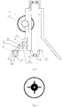
Fig. 1 is a schematic view showing an apparatus for detecting display panel defects according to a first exemplary embodiment of the disclosure; -
Fig. 2 is a cross-sectional view showing the apparatus for detecting display panel defects according to the first exemplary embodiment of the disclosure; -
Figs. 3 and4 are schematic bottom views showing a marking component of the apparatus for detecting display panel defects according to the first exemplary embodiment of the disclosure; -
Fig. 5 is a flowchart showing a method for detecting display panel defects according to a second exemplary embodiment of the disclosure; and -
Fig. 6 is a specific flowchart showing the method for detecting display panel defects according to the second exemplary embodiment of the disclosure. - To improve understanding of the technical solution of the present disclosure for those skilled in the art, the present disclosure will be described below in detail in conjunction with the accompanying drawings and specific embodiments.
- According to one aspect of the disclosure, this exemplary embodiment provides an apparatus for detecting display panel defects configured to detect a microscopic defect in a display panel. As shown in
Figs. 1 and2 , the apparatus for detecting display panel defects includes adetection component 1, amarking component 2 and aswitch component 3. Thedetection component 1 and themarking component 2 are both disposed on theswitch component 3 which is connected to amicroscope 10. Thedetection component 1 has a first visual area and is configured to detect a position of a microscopic defect in the display panel. Theswitch component 3 is configured so that themarking component 2 is rotated to the position of the microscopic defect after thedetection component 1 detects the position of the microscopic defect. Themarking component 2 has a second visual area with a smaller area than the first visual area. The second visual area is configured to determine a specific position of the microscopic defect in the first visual area including the position of the microscopic defect. The specific position is marked by themarking component 2. - In the exemplary embodiment, the apparatus for detecting display panel defects includes the
switch component 3 disposed on themicroscope 10, and thedetection component 1 and themarking component 2 connected to theswitch component 3. The first visual area of thedetection component 1 is larger than the second visual area of the markingcomponent 2. Thus, after thedetection component 1 detects the position of the microscopic defect in the display panel, the markingcomponent 2 may be rotated to the position of the microscopic defect by theswitch component 3. Next, the markingcomponent 2 determines and marks the specific position of the microscopic defect in the first visual area including the position of the microscopic defect. In short, firstly thedetection component 1 determines a larger scope (i.e., the first visual area) of the microscopic defect; and then the markingcomponent 2 determines a smaller scope (i.e., the second visual area) of the microscopic defect and directly marks the position of the microscopic defect in the first visual area including the microscopic defect. In the apparatus for detecting display panel defects according to the exemplary embodiment, after themarking component 2 detects the specific position of the microscopic defect, the specific position of the microscopic defect is directly marked by the markingcomponent 2 so as to avoid various disadvantages of manually marking the position of the microscopic defect in the display panel as in the existing art, thereby obtaining a more precise region of the microscopic defect and higher detection efficiency. - In the exemplary embodiment, a center of the first visual area of the
detection component 1 and a center of the second visual area of the markingcomponent 2 coincide after theswitch component 3 is rotated by 180°. - The reason for such setting lies in that after the
detection component 1 detects the first visual area including the microscopic defect, a position of thedetection component 1 may be adjusted so that the center of the first visual area of thedetection component 1 corresponds to the position of the microscopic defect. Next, the switch component is directly rotated by 180° so that the center of the second visual area of the markingcomponent 2 also falls into the position of the microscopic defect. Then, the markingcomponent 2 may directly mark the microscopic defect. Thus, the detection efficiency and precision of the microscopic defect are greatly improved. - In the exemplary embodiment, the apparatus for detecting display panel defects further includes a
drive component 4 via which theswitch component 3 is connected to themicroscope 10, thedrive component 4 being configured to drive theswitch component 3 to move upward and downward along an axial direction of themicroscope 10. - Specifically, when the
drive component 4 drives theswitch component 3 to move upward and downward along the axial direction of themicroscope 10, thedrive component 4 may drive thedetection component 1 and themarking component 2 to move upward and downward along the axial direction of themicroscope 10 so as to conduct detection of the position of the microscopic defect by thedetection component 1 and themarking component 2, as well as drive the markingcomponent 2 to mark the position of the microscopic defect. - In the exemplary embodiment, the
drive component 4 includes an in-focus spiral 41 and a threadedrod 42. The in-focus spiral 41 is fixed on themicroscope 10, and the threadedrod 42 is connected to the in-focus spiral 41 at one end and theswitch component 3 at the other end. At this time, the threadedrod 42 may be driven to move upward and downward by rotating the in-focus spiral 41 so as to adjust a distance between thedetection component 1 and themarking component 2 and the display panel, as well as drive the markingcomponent 2 to mark the position of the microscopic defect. - In the exemplary embodiment, the
switch component 3 includes a positioningmember 37, a rotatingshaft 33, and a carrying member. The positioningmember 37 has a hollow structure and is connected to thedrive component 4. The rotatingshaft 33 is disposed within the hollow structure of the positioningmember 37 and connected to the carrying member. The carrying member includes a first carryingpart 31 and a second carryingpart 32 connected to each other, the first carryingpart 31 is configured to carry thedetection component 1, and the second carryingpart 32 is configured to carry themarking component 2. - The rotating
shaft 33 is provided with afirst recess 36 in a direction perpendicular to an axis thereof. Aspring 34 and apositioning ball 35 are disposed sequentially within thefirst recess 36 along a direction of an opening of thefirst recess 36. Thespring 34 is fixed at a bottom of thefirst recess 36 at one end and connected to thepositioning ball 35 at the other end. The positioningmember 37 is provided with asecond recess 38 fitting to thepositioning ball 35 at an inner wall of the hollow structure thereof. At this time, a rotation position of therotating shaft 33 may be positioned by thepositioning ball 35. In the exemplary embodiment, the number of the second recesses 38 is two so that two rotation positions of therotating shaft 33 after being rotated by 180° are positioned, and thus a switch of positions of thedetection component 1 and themarking component 2 is realized. The present invention is not limited thereto; any suitable number of thesecond recesses 38 may be provided as needed. - In the exemplary embodiment, the first carrying
part 31 is threadedly connected to thedetection component 1; and the second carryingpart 32 is threadedly connected to themarking component 2. That is, the first carryingpart 31 and the second carryingpart 32 have inner threads while thedetection component 1 and themarking component 2 have outer threads. - The reason for adopting the threaded connection lies in that threaded connection facilitates replacement of the
detection component 1 and themarking component 2. In addition, by the threaded connection, thedetection component 1 and themarking component 2 can be fixed in the first carryingpart 31 and the second carryingpart 32 respectively so as to prevent thedetection component 1 and themarking component 2 from waggling due to rotation of therotating shaft 33 or driving of thedrive component 4 during detection of the microscopic defect, and thus influencing the precision in detection. - In the exemplary embodiment, after the
marking component 2 is placed on the second carryingpart 32 and thedetection component 1 is placed on the first carryingpart 31, the distance between the markingcomponent 2 and the display panel is about 2 mm smaller than the distance between thedetection component 1 and the display panel. Thus, it is ensured that the distance between the markingcomponent 2 and the display panel is smaller than the distance between thedetection component 1 and the display panel so as to prevent thedetection component 1 coming into contact with the display panel and thus prevent the display panel from being scratched when the markingcomponent 2 marks the microscopic defect. - In the exemplary embodiment, the
detection component 1 has an objective with a first magnification, and themarking component 2 has an objective with a second magnification greater than the first magnification. Thus, a region including the microscopic defect may be detected firstly by the objective with a smaller magnification, and then, by switching to the objective with a greater magnification (e.g., a 50× objective), a region smaller than the region including the microscopic defect detected by the objective with a smaller magnification is determined. In this method, the marking precision of the microscopic defect is improved, the microscopic defect is marked more quickly and thus the overall marking efficiency is increased. - In the exemplary embodiment, the marking
component 2 includes anobservation part 21 and a raisedpart 22 at a side of theobservation part 21 proximal to the display panel. Theobservation part 21 is used to observe the position of the microscopic defect in the display panel, and the raisedpart 22 is used to mark a region including the position of the microscopic defect after coloring. As shown inFigs. 3 and4 , the raisedpart 22 has a marking pattern including any one of parallel lines, circle, rectangle and triangle. - In the exemplary embodiment, a height of the raised
part 22 on themarking component 2 may be any suitable height, and a diameter of theobservation part 21 matches a size of the microscopic defect. Apparently, asuitable marking component 2 may be used instead dependent on the size of the microscopic defect. - According to another aspect of the disclosure, this exemplary embodiment provides a method for detecting display panel defects using the apparatus for detecting display panel defects of the first exemplary embodiment. As shown in
Fig. 5 , the method comprises the steps of: - by the
detection component 1, detecting a position of a microscopic defect in a display panel, and determining a first visual area including the position of the microscopic defect; - rotating the marking
component 2 to the position of the microscopic defect by theswitch component 3 after thedetection component 1 detects the position of the microscopic defect; - by the marking
component 2, determining and marking a specific position of the microscopic defect in the first visual area including the position of the microscopic defect (i.e., determining a second visual area including the position of the microscopic smaller than the first visual area within the first visual area including the position of the microscopic defect). - In the method for detecting display panel defects of the exemplary embodiment, after the
detection component 1 detects the position of the microscopic defect in the display panel, the markingcomponent 2 may be rotated to the position of the microscopic defect by theswitch component 3. Next, the markingcomponent 2 determines and marks the specific position of the microscopic defect in the first visual area including the position of the microscopic defect. In short, firstly thedetection component 1 determines a larger scope (i.e., the first visual area) of the microscopic defect; and then the markingcomponent 2 determines a smaller scope (i.e., the second visual area) of the microscopic defect and directly marks the position of the microscopic defect in the first visual area including the microscopic defect. In the apparatus for detecting display panel defects according to the exemplary embodiment, after themarking component 2 detects the specific position of the microscopic defect, the specific position of the microscopic defect is directly marked by the markingcomponent 2 so as to avoid various disadvantages of manually marking the position of the microscopic defect in the display panel as in the existing art, thereby obtaining a more precise region of the microscopic defect and higher detection efficiency. - The method for detecting display panel defects according to the exemplary embodiment will now be described in detail under the following conditions: the
detection component 1 has an objective with a first magnification (i.e., thedetection component 1 is an objective lens), and themarking component 2 has an objective with a second magnification (i.e., the markingcomponent 2 is a mark lens) greater than the first magnification; a center of the first visual area of thedetection component 1 and a center of the second visual area of the markingcomponent 2 coincide after theswitch component 3 is rotated by 180°; theswitch component 3 includes a positioningmember 37, a rotatingshaft 33, a first carryingpart 31 and a second carryingpart 32; and thedrive component 4 includes an in-focus spiral 41 and a threadedrod 42. As shown inFig. 6 , the method specifically comprises the steps of: - Step S1, calibrating the mark lens. Specifically, coinciding the observation part (a position of the hole in the mark lens) of the mark lens with a mark at the center of the objective lens after the
switch component 3 is rotated by 180° so as to complete calibration of the mark lens. - Step S2, by the objective lens, determining the position of the microscopic defect in the display panel, and determining a size of the microscopic defect, i.e., determining the first visual area including the position of the microscopic defect. If the size of the microscopic defect is about 200 µm, a mark lens with a diameter of about 300 µm is selected.
- Step S3, determining whether the mark lens meets requirements; if not, selecting a corresponding mark lens and returning to S2.
- Step S4, rotating the mark lens to a position of the objective lens by rotating the
rotating shaft 33. - Step S5, rotating the in-
focus spiral 41 so that the mark lens is moved down to the position of the microscopic defect in the display panel, and marking the position of the microscopic defect through coloring by a lower part of the mark lens. - Step S6, rotating the objective lens to a position of the mark lens by rotating the
rotating shaft 33 so as to determine a marking effect of the mark lens on the microscopic defect; if there is no problem, the procedure is ended; if the mark does not meet the requirements, erasing the mark and returning to S2 to mark again. - According to yet another aspect of the disclosure, this exemplary embodiment provides a
microscope 10 comprising the apparatus for detecting display panel defects of the first exemplary embodiment to mark a position of a microscopic defect in a display panel. - It should be understood that the above embodiments are merely exemplary embodiments for the purpose of illustrating the principle of the disclosure, and the disclosure is not limited thereto. Various modifications and improvements can be made by a person having ordinary skill in the art without departing from the spirit and essence of the disclosure. Accordingly, all of the modifications and improvements also fall into the protection scope of the disclosure.
Claims (15)
- An apparatus for detecting display panel defects comprising:a switch component (3), which is connected to a microscope (10);a detection component (1), which is disposed on the switch component (3) and has a first visual area, the detection component (1) being configured to detect a position of a microscopic defect in a display panel; anda marking component (2), which is disposed on the switch component (3) and has a second visual area with a smaller area than the first visual area, the marking component (2) being configured to mark the position of the microscopic defect in the display panel,wherein the switch component (3) is configured to rotate the marking component (2) to a position of the detection component (1) and mark a position of the microscopic defect by the marking component (2) after the detection component (1) detects the position.
- The apparatus for detecting display panel defects according to claim 1,
wherein the marking component (2) comprises:an observation part (21), which is configured to observe the position of the microscopic defect in the display panel; anda raised part (22), which is disposed at a side of the observation part (21) proximal to the display panel and has a colorant for marking the position of the microscopic defect. - The apparatus for detecting display panel defects according to claim 2,
wherein the raised part (22) has a marking pattern including any one of parallel lines, circle, rectangle and triangle. - The apparatus for detecting display panel defects according to claim 1, further comprising:
a drive component (4) via which the switch component (3) is connected to the microscope (10), the drive component (4) being configured to drive the switch component (3) to move upward and downward along an axial direction of the microscope (10). - The apparatus for detecting display panel defects according to claim 4,
wherein the drive component (4) comprises:an in-focus spiral (41), which is fixed on the microscope (10); anda threaded rod (42), which is connected to the in-focus spiral (41) at one end and the switch component (3) at the other end. - The apparatus for detecting display panel defects according to claim 4,
wherein the switch component (3) comprises:a positioning member (37), which has a hollow structure and is connected to the drive component (4);a rotating shaft (33), which is disposed within the hollow structure of the positioning member (37); anda carrying member, which is connected to the rotating shaft (33) and has a first carrying part (31) and a second carrying part (32) connected to each other, the first carrying part (31) being configured to carry the detection component (1), and the second carrying part (32) being configured to carry the marking component (2). - The apparatus for detecting display panel defects according to claim 6,
wherein the rotating shaft (33) is provided with a first recess (36) in a direction perpendicular to an axis thereof, a spring (34) and a positioning ball (35) are disposed sequentially within the first recess (36) along a direction of an opening of the first recess (36), the spring (34) is fixed at a bottom of the first recess (36) at one end and connected to the positioning ball (35) at the other end; and
the positioning member (37) is provided with a second recess (38) fitting to the positioning ball (35) at an inner wall of the hollow structure thereof. - The apparatus for detecting display panel defects according to claim 6,
wherein the first carrying part (31) is threadedly connected to the detection component (1), and the second carrying part (32) is threadedly connected to the marking component (2). - The apparatus for detecting display panel defects according to claim 6,
wherein after the marking component (2) is placed on the second carrying part (32) and the detection component (1) is placed on the first carrying part (31), a distance between the marking component (2) and the detected display panel is about 2 mm smaller than a distance between the detection component (1) and the detected display panel. - The apparatus for detecting display panel defects according to claim 1,
wherein the detection component (1) has an objective with a first magnification, and the marking component (2) has an objective with a second magnification greater than the first magnification. - The apparatus for detecting display panel defects according to claim 1,
wherein a center of the first visual area and a center of the second visual area coincide after the switch component (3) is rotated by 180°. - A method for detecting display panel defects using the apparatus for detecting display panel defects according to claim 1, the method comprising:by the detection component (1), detecting a position of a microscopic defect in a display panel, and determining a first visual area including the position of the microscopic defect;by the switch component (3), rotating the marking component (2) to a position of the detection component (1) after the detection component (1) detects the position of the microscopic defect; andby the marking component (2), determining and marking a specific position of the microscopic defect in the first visual area including the position of the microscopic defect.
- The method for detecting display panel defects according to claim 12,
wherein before the step of by the detection component (1), detecting the position of the microscopic defect in the display panel, and determining the first visual area including the position of the microscopic defect, the method further comprises the step of:
calibrating the marking component (2) so that a center of the first visual area and a center of the second visual area coincide after the switch component (3) is rotated by 180°. - The method for detecting display panel defects according to claim 13,
wherein the step of by the detection component (1), detecting the position of the microscopic defect in the display panel, and determining the first visual area including the position of the microscopic defect specifically includes:
by the detection component (1), detecting a position of a microscopic defect in a display panel, aligning the position of the microscopic defect with a center of the detection component (1), and then determining a first visual area including the position of the microscopic defect. - A microscope comprising the apparatus for detecting display panel defects according to claim 1.
Applications Claiming Priority (2)
| Application Number | Priority Date | Filing Date | Title |
|---|---|---|---|
| CN201710329998.3A CN108872240A (en) | 2017-05-11 | 2017-05-11 | Microdefect detection device and detection method, microscope |
| PCT/CN2017/115454 WO2018205592A1 (en) | 2017-05-11 | 2017-12-11 | Detection apparatus and detection method for defect of display panel, and microscope |
Publications (2)
| Publication Number | Publication Date |
|---|---|
| EP3623800A1 true EP3623800A1 (en) | 2020-03-18 |
| EP3623800A4 EP3623800A4 (en) | 2021-01-20 |
Family
ID=64104828
Family Applications (1)
| Application Number | Title | Priority Date | Filing Date |
|---|---|---|---|
| EP17898327.6A Withdrawn EP3623800A4 (en) | 2017-05-11 | 2017-12-11 | DISPLAY PANEL FAULT DETECTION DETECTION AND METHOD, AND MICROSCOPE |
Country Status (4)
| Country | Link |
|---|---|
| US (1) | US20210209789A1 (en) |
| EP (1) | EP3623800A4 (en) |
| CN (1) | CN108872240A (en) |
| WO (1) | WO2018205592A1 (en) |
Families Citing this family (4)
| Publication number | Priority date | Publication date | Assignee | Title |
|---|---|---|---|---|
| CN109580636B (en) * | 2018-12-03 | 2021-11-02 | 深圳市华星光电半导体显示技术有限公司 | Display panel defect marking tool |
| CN110542687A (en) * | 2019-07-02 | 2019-12-06 | 中国工程物理研究院激光聚变研究中心 | Detection device and detection method for appearance defects of microscopic elements |
| JP7506523B2 (en) * | 2020-05-20 | 2024-06-26 | 株式会社エビデント | Microscope system, control method, and program |
| CN119666535B (en) * | 2024-12-17 | 2025-10-10 | 吉林大学 | A surface defect indentation marking and rapid indentation response testing device and method |
Family Cites Families (15)
| Publication number | Priority date | Publication date | Assignee | Title |
|---|---|---|---|---|
| JP2000046750A (en) * | 1998-07-30 | 2000-02-18 | Advanced Display Inc | Surface defect confirming apparatus, substrate defect analyzing method using the same and substrate defect analyzing method of liquid crystal display apparatus |
| JP4320132B2 (en) * | 2001-05-24 | 2009-08-26 | レーザーテック株式会社 | Defect observation method and defect observation apparatus |
| DE102005029381B4 (en) * | 2005-06-24 | 2007-04-26 | Olympus Soft Imaging Solutions Gmbh | Method and apparatus for optically scanning a sample |
| JP4942430B2 (en) * | 2006-09-07 | 2012-05-30 | Ntn株式会社 | Pattern correction method and pattern correction apparatus |
| CN101726504B (en) * | 2009-12-17 | 2011-09-07 | 丹东华日理学电气有限公司 | Defect positioning and marking method for digital flat-panel X-ray detection system |
| JP2011099875A (en) * | 2011-02-18 | 2011-05-19 | Olympus Corp | Visual inspection apparatus |
| CN102854195B (en) * | 2012-09-21 | 2014-08-20 | 京东方科技集团股份有限公司 | Method for detecting defect coordinates on color filter |
| JP5978162B2 (en) * | 2013-03-29 | 2016-08-24 | 株式会社日立ハイテクノロジーズ | Defect inspection method and defect inspection apparatus |
| CN103604812A (en) * | 2013-10-23 | 2014-02-26 | 上海华力微电子有限公司 | Multipoint positioning method for wafer macroscopic defect |
| JP6094457B2 (en) * | 2013-11-05 | 2017-03-15 | 株式会社島津製作所 | Hardness testing machine |
| CN104752252A (en) * | 2013-12-30 | 2015-07-01 | 中芯国际集成电路制造(上海)有限公司 | Crystal back defect representation method |
| CN103969567A (en) * | 2014-04-22 | 2014-08-06 | 四川虹视显示技术有限公司 | Method and device for detecting and analyzing defects of OLED device |
| CN104317079B (en) * | 2014-10-29 | 2017-12-01 | 京东方科技集团股份有限公司 | A kind of display panel identifying system, detecting system, recognition methods and detection method |
| CN106290376B (en) * | 2016-07-21 | 2019-04-12 | 京东方科技集团股份有限公司 | Microdefect detection device and its control method, microscope |
| CN206710328U (en) * | 2017-05-11 | 2017-12-05 | 京东方科技集团股份有限公司 | Microdefect detection means and microscope |
-
2017
- 2017-05-11 CN CN201710329998.3A patent/CN108872240A/en active Pending
- 2017-12-11 WO PCT/CN2017/115454 patent/WO2018205592A1/en not_active Ceased
- 2017-12-11 EP EP17898327.6A patent/EP3623800A4/en not_active Withdrawn
- 2017-12-11 US US15/778,442 patent/US20210209789A1/en not_active Abandoned
Also Published As
| Publication number | Publication date |
|---|---|
| WO2018205592A1 (en) | 2018-11-15 |
| EP3623800A4 (en) | 2021-01-20 |
| US20210209789A1 (en) | 2021-07-08 |
| CN108872240A (en) | 2018-11-23 |
Similar Documents
| Publication | Publication Date | Title |
|---|---|---|
| US20210209789A1 (en) | Apparatus and Method for Detecting Display Panel Defects and Microscope | |
| CN101893434B (en) | Roundness Meter | |
| JP2017090106A (en) | Inspection tool for structures | |
| KR20070116721A (en) | How to measure eccentricity | |
| CN111623709B (en) | Image measuring instrument capable of automatically adjusting position of sample to be measured and measuring method | |
| DE102013213599B4 (en) | Method and device for spectrometric reflection measurement on spherical surfaces | |
| JP4925644B2 (en) | Coating mechanism, defect correction apparatus, coating method, and defect correction method for color filter for liquid crystal display panel | |
| CN110455814A (en) | The detection method of needle-shaped foreign matter ingredient in a kind of electronic glass | |
| US12055556B2 (en) | Manipulation system and driving method of manipulation system | |
| JP6623304B2 (en) | Nozzle position measurement method and collection system | |
| JP2005268486A (en) | Marking method, marking apparatus and test device | |
| CN206710328U (en) | Microdefect detection means and microscope | |
| KR100956894B1 (en) | Precision measurement device | |
| CN107688230B (en) | Microscope for marking bad lines of liquid crystal screen | |
| CN104777234A (en) | Device and method for ultrasonic probe positioning by utilizing camera | |
| CN204536278U (en) | Camera is utilized to carry out the device of ultrasonic probe location | |
| JP6040816B2 (en) | Hardness testing machine | |
| US20190225927A1 (en) | Collection method for fine particles and collection system | |
| CN209232737U (en) | A kind of flaw labeling device | |
| KR100532909B1 (en) | Method and Apparatus for Aligning a Axial Centerline in Gripping | |
| JP2019100928A (en) | Lens shape measurement device | |
| JP3941867B2 (en) | Axis centering method and apparatus for gripping center | |
| KR20090020259A (en) | A defect point detector of glass panel | |
| CN221198335U (en) | PBN thin-wall workpiece detection device | |
| JP4547890B2 (en) | Marking device, objective lens, and upright microscope |
Legal Events
| Date | Code | Title | Description |
|---|---|---|---|
| STAA | Information on the status of an ep patent application or granted ep patent |
Free format text: STATUS: UNKNOWN |
|
| STAA | Information on the status of an ep patent application or granted ep patent |
Free format text: STATUS: THE INTERNATIONAL PUBLICATION HAS BEEN MADE |
|
| PUAI | Public reference made under article 153(3) epc to a published international application that has entered the european phase |
Free format text: ORIGINAL CODE: 0009012 |
|
| STAA | Information on the status of an ep patent application or granted ep patent |
Free format text: STATUS: REQUEST FOR EXAMINATION WAS MADE |
|
| 17P | Request for examination filed |
Effective date: 20180903 |
|
| AK | Designated contracting states |
Kind code of ref document: A1 Designated state(s): AL AT BE BG CH CY CZ DE DK EE ES FI FR GB GR HR HU IE IS IT LI LT LU LV MC MK MT NL NO PL PT RO RS SE SI SK SM TR |
|
| AX | Request for extension of the european patent |
Extension state: BA ME |
|
| DAV | Request for validation of the european patent (deleted) | ||
| DAX | Request for extension of the european patent (deleted) | ||
| R17P | Request for examination filed (corrected) |
Effective date: 20180903 |
|
| A4 | Supplementary search report drawn up and despatched |
Effective date: 20201223 |
|
| RIC1 | Information provided on ipc code assigned before grant |
Ipc: G02B 21/24 20060101ALI20201217BHEP Ipc: G01N 21/88 20060101AFI20201217BHEP |
|
| STAA | Information on the status of an ep patent application or granted ep patent |
Free format text: STATUS: EXAMINATION IS IN PROGRESS |
|
| 17Q | First examination report despatched |
Effective date: 20210908 |
|
| STAA | Information on the status of an ep patent application or granted ep patent |
Free format text: STATUS: THE APPLICATION IS DEEMED TO BE WITHDRAWN |
|
| 18D | Application deemed to be withdrawn |
Effective date: 20220119 |