EP3623757B1 - Spintronic gyroscopic sensor device - Google Patents
Spintronic gyroscopic sensor device Download PDFInfo
- Publication number
- EP3623757B1 EP3623757B1 EP19195761.2A EP19195761A EP3623757B1 EP 3623757 B1 EP3623757 B1 EP 3623757B1 EP 19195761 A EP19195761 A EP 19195761A EP 3623757 B1 EP3623757 B1 EP 3623757B1
- Authority
- EP
- European Patent Office
- Prior art keywords
- layer
- free layer
- tunnel barrier
- pinned
- mtj element
- Prior art date
- Legal status (The legal status is an assumption and is not a legal conclusion. Google has not performed a legal analysis and makes no representation as to the accuracy of the status listed.)
- Active
Links
Images










Classifications
-
- G—PHYSICS
- G01—MEASURING; TESTING
- G01C—MEASURING DISTANCES, LEVELS OR BEARINGS; SURVEYING; NAVIGATION; GYROSCOPIC INSTRUMENTS; PHOTOGRAMMETRY OR VIDEOGRAMMETRY
- G01C19/00—Gyroscopes; Turn-sensitive devices using vibrating masses; Turn-sensitive devices without moving masses; Measuring angular rate using gyroscopic effects
- G01C19/56—Turn-sensitive devices using vibrating masses, e.g. vibratory angular rate sensors based on Coriolis forces
- G01C19/5776—Signal processing not specific to any of the devices covered by groups G01C19/5607 - G01C19/5719
-
- H—ELECTRICITY
- H01—ELECTRIC ELEMENTS
- H01F—MAGNETS; INDUCTANCES; TRANSFORMERS; SELECTION OF MATERIALS FOR THEIR MAGNETIC PROPERTIES
- H01F10/00—Thin magnetic films, e.g. of one-domain structure
- H01F10/32—Spin-exchange-coupled multilayers, e.g. nanostructured superlattices
- H01F10/324—Exchange coupling of magnetic film pairs via a very thin non-magnetic spacer, e.g. by exchange with conduction electrons of the spacer
- H01F10/3254—Exchange coupling of magnetic film pairs via a very thin non-magnetic spacer, e.g. by exchange with conduction electrons of the spacer the spacer being semiconducting or insulating, e.g. for spin tunnel junction [STJ]
-
- H—ELECTRICITY
- H10—SEMICONDUCTOR DEVICES; ELECTRIC SOLID-STATE DEVICES NOT OTHERWISE PROVIDED FOR
- H10B—ELECTRONIC MEMORY DEVICES
- H10B61/00—Magnetic memory devices, e.g. magnetoresistive RAM [MRAM] devices
-
- H—ELECTRICITY
- H10—SEMICONDUCTOR DEVICES; ELECTRIC SOLID-STATE DEVICES NOT OTHERWISE PROVIDED FOR
- H10N—ELECTRIC SOLID-STATE DEVICES NOT OTHERWISE PROVIDED FOR
- H10N50/00—Galvanomagnetic devices
- H10N50/80—Constructional details
-
- H—ELECTRICITY
- H10—SEMICONDUCTOR DEVICES; ELECTRIC SOLID-STATE DEVICES NOT OTHERWISE PROVIDED FOR
- H10N—ELECTRIC SOLID-STATE DEVICES NOT OTHERWISE PROVIDED FOR
- H10N59/00—Integrated devices, or assemblies of multiple devices, comprising at least one galvanomagnetic or Hall-effect element covered by groups H10N50/00 - H10N52/00
Definitions
- This disclosure relates to sensor devices and, more specifically, to spintronic-based devices that are configured to detect gyroscopic motion.
- Some devices include a gyroscopic sensor device that monitors gyroscopic motion of a device. It is desirable for such devices to detect gyroscopic motion of the device to provide context of the device. For example, a position of the device may be controlled based on the gyroscopic motion of the device. It is generally desirable for a gyroscopic sensor device to measure accurately gyroscopic motion and to operate in a smaller space.
- Current types of gyroscopic sensor devices include non-magnetic sensors that generate a voltage in response changes in angular velocity of the device.
- US5859368 discloses a tunnelling-based rotation rate sensor.
- US5905202 discloses a tunnelling rotation sensor.
- CN104567848 discloses a micromechanical gyroscope based on the tunnel magnetoresistive effect.
- CN102853826 discloses a silicon based tunneling magnetoresistance micro gyroscope.
- CN105180914 discloses an in-plane detection micromechanical gyroscope.
- This disclosure generally describes techniques for detecting gyroscopic motion using a spintronic-based sensor device.
- the techniques may in some instances provide for a higher density for a smaller and more lightweight form factor.
- a spintronic-based sensor device may be more resistive to ElectroMagnetic Interference (EMI) than non-magnetic sensors, which may be of particular benefit to certain applications.
- EMI ElectroMagnetic Interference
- the invention includes a magnetic tunnel junction (MTJ) based sensor device according to claim 1 and a method for detecting gyroscopic motion using a MTJ based sensor device according to claim 16.
- MTJ magnetic tunnel junction
- sensing devices may be configurable for strategic applications.
- such sensing devices may be radiation-hardened, and to include magnetically-based devices that can be integrated (e.g., monolithically, in particular initially) into a compact module with Application-Specific Integrated Circuits (ASICs) including those that contain embedded Magnetoresistive Random Access Memory (MRAM) bits.
- ASICs Application-Specific Integrated Circuits
- MRAM Magnetoresistive Random Access Memory
- gyroscope sensor device that could be used with or separately from other sensors (e.g., an acceleration sensor, a mechanical shock and vibration sensor, etc.), and that may support compatibility with MRAM technology.
- circuitry may be constructed to include a magnetic tunnel junction (MTJ), which is an example of a spintronic device, with desired, resistance, resistance-area product, and dimensions.
- MTJ magnetic tunnel junction
- resistance and/or magnetoresistance may include, but are not limited to, tunnel magnetoresistance (TMR), giant magnetoresistance (GMR), anisotropic magnetoresistive (AMR), and other resistance and/or magnetoresistance effects.
- test structure(s) such as rectangular, square, circular, ovoid, or quasi-circular shape(s) with designed symmetries and/or asymmetries and placed in a circular or similar arrangement, that can be tethered/suspended to respond to pivoting and/or torsional displacements and rotations.
- the test structure(s) can be constructed from and/or coated with a magnetic material that may be patterned.
- Processing circuitry may make use electrical, electronic, or spintronic current(s).
- Tunneling current(s) can be spin-dependent or spin-independent, and ballistic electron tunneling may be used.
- Anisotropic, Giant, and/or Tunneling Magneto-Resistive effects may be used for sensing gyroscope motion.
- a free layer may flex towards and/or away from each one of a plurality of pinned layers. Such flexing by the free layer may cause corresponding changes in resistance of the MTJ formed by the free layer and each one of the plurality of pinned layers. In this way, processing circuitry may detect gyroscopic motion using the resistance of the MTJ.
- Such magnetic/spintronic devices may provide unique and desired application functionality, customization prospects, and environmental capability (e.g., shock, vibration, radiation, acceleration, motion) for various environments.
- Such magnetic/spintronic devices may offer materials and technological similarity and compatibility with MRAM bits and other sensing devices such as accelerometers, gyros, and pressure sensors, which may support integration, modularity, miniaturization, and packaging with embedded MRAM and ASICS.
- the spintronic-based gyroscopic sensor device described herein may be used for die-to-die or monolithic integration with MTJs/MTJ die.
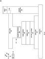
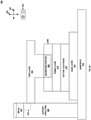
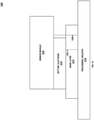
- FIG. 1A shows a conceptual illustration of a cross-sectional view of a first magnetic tunnel junction (MTJ) element 100 configured to gyroscopic motion.
- MTJ element 100 may include support structure 102, free layer 104, tunnel barrier 108, pinned layer 110, bottom electrode 112, base layer 114, and substrate 116.
- support structure 102 extends from substrate 116 along vertical direction 140 and is spaced apart from tunnel barrier 108 along first horizontal direction 142.
- Second horizontal direction 144 is perpendicular to first horizontal direction 142 and vertical direction 140.
- Base layer 114 may comprise, for example, silicon (Si).
- Substrate 116 may comprise, for example, silicon (Si).
- substrate 116 may include processing circuitry.
- substrate 116 may include metallization and/or integrated circuitry (e.g., Complementary metal-oxide-semiconductor (CMOS)).
- CMOS Complementary metal-oxide-semiconductor
- Support structure 102 may be adapted to arrange free layer 104 above tunnel barrier 108.
- Support structure 102 may be formed of silicon, silicon nitride, silicon oxide, copper, aluminum, aluminum oxide, magnesium oxide, or another material.
- support structure 102 may include via 120 and metal 118.
- Via 120 and metal 118 may be formed of a conductive material to permit a connection to MTJ element 100. Examples of conductive materials may include, but are not limited to, copper.
- Bottom electrode 112 may be formed of a conductive material to permit a connection to MTJ element 100.
- support structure 102 is arranged right of tunnel barrier 508 along first horizontal direction 142.
- support structure 102 is arranged left of tunnel barrier 508 along first horizontal direction 142.
- Support structure 102 may be arranged above and/or below tunnel barrier 108 along second horizontal direction 144.
- Free layer 104 may include a magnetization direction that is free to switch between a parallel orientation and an antiparallel orientation. As shown, free layer 104 may include magnetized portion 106. In the example of FIG. 1 , magnetized portion 106 is arranged above tunnel barrier 108. Magnetized portion 106 may include, for example, but not limited to, a metal and/or a metal/ferromagnetic metal system. For instance, magnetized portion 106 may be formed of a metal or metal/ferromagnetic metal system on Silicon Oxide (SiOx), Silicon Nitride (SiNx), and/or Silicon (Si).
- SiOx Silicon Oxide
- SiNx Silicon Nitride
- Si Silicon
- Tunnel barrier 108 includes a non-magnetic metal that separates free layer 104 and pinned layer 110.
- tunnel barrier 108 may be formed of aluminum oxide, magnesium oxide, or another material.
- free layer 104 and/or magnetized portion 106 is spaced apart from tunnel barrier 108 along vertical direction 140.
- a void may separate free layer 104 and tunnel barrier 108.
- a void may separate magnetized portion 106 and tunnel barrier 108.
- a bottom portion of free layer 104 may be adjacent to a top portion of tunnel barrier 108 along vertical direction 140.
- free layer 104 and/or magnetized portion 106 is spaced next to tunnel barrier 108 along vertical direction 140.
- Pinned layer 110 includes a magnetization direction that is fixed or "pinned" to a single orientation.
- pinned layer 110 may be pinned in a parallel orientation.
- pinned layer 110 may be pinned in an antiparallel orientation.
- pinned layer 110 includes an anti-ferromagnetic layer, such that the magnetization direction of the pinned layer 110 is "pinned" in a particular orientation. The magnetization direction of the pinned layer 110 remains relatively fixed when operational magnetic fields are applied to MTJ element 100.
- MTJ element 100 may be formed as follows. Initially, material for tunnel barrier 108 and pinned layer 110 is deposited. An oxide is formed on tunnel barrier 108 and tunnel barrier 108 and pinned layer 110 are etched. Tunnel barrier 108 and pinned layer 110 are encapsulated (for spacing). Material for free layer 104 (which can be rectangular or triangular, e.g., in area) and support structure 102 are deposed (with a top electrode for connection to metallization). The encapsulating material is removed and/or dissolved.
- a magnetization direction of free layer 104 is used to detect a gyroscopic motion of MTJ element 100.
- portion 107 of free layer 104 may flex in response to gyroscopic motion, resulting in a corresponding change in resistance and/or magnetoresistance of MTJ element 100.
- processing circuitry may detect gyroscopic motion using the resistance and/or magnetoresistance of the MTJ element 100. In this manner, MTJ element 100 may be used as a gyroscopic motion sensor.
- FIG. 1B shows a conceptual illustration of a top-view of the first MTJ element 100 of FIG. 1A .
- first MTJ element 100 includes tunnel barriers 130, 132, and 134, each one of which may be substantially similar to tunnel barrier 108.
- each one of tunnel barriers 130, 132, and 134 may include a corresponding pinned layer and bottom electrode.
- each tunnel barrier of tunnel barriers 108, 130, 132, and 134 may be arranged above a respective pinned layer.
- tunnel barriers 108, 130, 132, and 134 (and respective pinned layers) are arranged relative to free layer 104 to detect a square motion 160.
- tunnel barriers 108, 130, 132, and 134 (and respective pinned layers) may be arranged relative to free layer 104 to detect a rectangular motion.
- tunnel barrier 130 is arranged right of free layer 104 along first horizontal direction 142.
- tunnel barrier 132 is arranged left of free layer 104 along first horizontal direction 142.
- tunnel barrier 132 is arranged along first horizontal direction 142 on an opposite side of free layer 104 from tunnel barrier 130.
- tunnel barrier 108 is arranged below free layer 104 along second horizontal direction 144.
- tunnel barrier 134 is arranged above free layer 104 along second horizontal direction 144.
- tunnel barrier 108 is arranged along second horizontal direction 144 on an opposite side of free layer 104 from tunnel barrier 134.
- magnetized portion 106 is centered to be approximately equidistant from tunnel barriers 108, 130, 132, and 134 along first horizontal direction 142 and second horizontal direction 144.
- FIG. 1C shows a conceptual illustration of a cross-sectional view of the first MTJ element 100 of FIG. 1A during first angular velocity 150.
- portion 107 of free layer 104 flexes toward tunnel barrier 108 along second horizontal direction 144 in response to first angular velocity 150.
- magnetized portion 106 is arranged closer to tunnel barrier 108 than tunnel barrier 134, which reduces a resistance and/or magnetoresistance between free layer 104 and a pinned layer below tunnel barrier 108.
- FIG. ID shows a conceptual illustration of a cross-sectional view of the first MTJ element 100 of FIG. 1A during a second angular velocity 152.
- portion 107 of free layer 104 flexes toward tunnel barrier 130 along first horizontal direction 142 in response to second angular velocity 152.
- magnetized portion 106 is arranged closer to tunnel barrier 130 than tunnel barrier 132, which reduces a resistance and/or magnetoresistance between free layer 104 and a pinned layer below tunnel barrier 134.
- FIG. 2A shows a conceptual illustration of a cross-sectional view of a second MTJ element 200 configured to detect gyroscopic motion.
- MTJ element 200 may include support structure 202, free layer 204, magnetized portion 206, tunnel barrier 208, pinned layer 210, bottom electrode 212, base layer 214, substrate 216, metal 218, and via 220, which may be examples of support structure 102, free layer 104, magnetized portion 106, tunnel barrier 108, pinned layer 110, bottom electrode 112, base layer 114, substrate 116, metal 118, and via 120 of FIG. 1 , respectively.
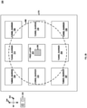
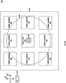
- FIG. 2B shows a conceptual illustration of a top-view of the second MTJ element 200 of FIG. 2A .
- second MTJ element 200 includes tunnel barriers 230, 232, 234, and 235-238, each one of which may be substantially similar to tunnel barrier 108 of FIG. 1 .
- each one of tunnel barriers 230, 232, 234, and 235-238 may include a corresponding pinned layer and bottom electrode.
- each tunnel barrier of tunnel barriers 230, 232, 234, and 235-238 may be arranged above a respective pinned layer.
- tunnel barriers 208, 230, 232, 234, and 235-238 are arranged relative to free layer 204 to detect a circular motion 260.
- tunnel barriers 230, 232, 234, and 235-238 may be arranged relative to free layer 204 to detect ovoid motion. In some examples, tunnel barriers 230, 232, 234, and 235-238 may be arranged relative to free layer 204 to detect quasi-circular motion.
- tunnel barrier 230 is arranged right of free layer 204 along first horizontal direction 242.
- tunnel barrier 232 is arranged left of free layer 204 along first horizontal direction 242.
- tunnel barrier 232 is arranged along first horizontal direction 242 on an opposite side of free layer 204 from tunnel barrier 230.
- tunnel barrier 208 is arranged below free layer 204 along second horizontal direction 244.
- tunnel barrier 234 is arranged above free layer 204 along second horizontal direction 244.
- tunnel barrier 208 is arranged along second horizontal direction 244 on an opposite side of free layer 204 from tunnel barrier 234.
- tunnel barrier 235 is arranged left of free layer 204 along first horizontal direction 242 and above free layer 204 along second horizontal direction 244.
- Tunnel barrier 236 may be arranged right of free layer 204 along first horizontal direction 242 and above free layer 204 along second horizontal direction 244.
- Tunnel barrier 237 is arranged left of free layer 204 along first horizontal direction 242 and below free layer 204 along second horizontal direction 244.
- Tunnel barrier 238 is arranged right of free layer 204 along first horizontal direction 242 and below free layer 204 along second horizontal direction 244.
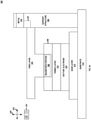
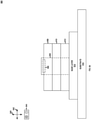
- FIG. 3A shows a conceptual illustration of a cross-sectional view of a third MTJ element 300 configured to detect gyroscopic motion.
- MTJ element 300 may include support structure 302, free layer 304, magnetized portion 306, tunnel barrier 308, pinned layer 310, bottom electrode 312, base layer 314, substrate 316, metal 318, and via 320, which may be examples of support structure 102, free layer 104, magnetized portion 106, tunnel barrier 108, pinned layer 110, bottom electrode 112, base layer 114, substrate 116, metal 118, and via 120 of FIG. 1 , respectively.
- free layer 304 is spaced next to tunnel barrier 308 along vertical direction 340.
- magnetized portion 306 is spaced next to tunnel barrier 308 along vertical direction 340.
- magnetized portion 306 may be arranged above pinned layer 310 and coplanar with tunnel barrier 308.
- free layer 304 and/or magnetized portion 306 may be arranged above pinned layer 310 along vertical direction 340.
- FIG. 3B shows a conceptual illustration of a top-view of the third MTJ element 300 of FIG. 3A .
- third MTJ element 300 includes tunnel barriers 308, 330, 332, and 334, each one of which may be substantially similar to tunnel barrier 108 of FIG. 1 .
- each one of tunnel barriers 330, 332, and 334 may include a corresponding pinned layer and bottom electrode.
- each tunnel barrier of tunnel barriers 308, 330, 332, and 334 may be arranged above a respective pinned layer.
- tunnel barriers 308, 330, 332, and 334 (and respective pinned layers) are arranged relative to free layer 304 to detect a square motion 360.
- tunnel barriers 308, 330, 332, and 334 (and respective pinned layers) may be arranged relative to free layer 304 to detect rectangular motion.
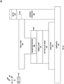
- FIG. 4A shows a conceptual illustration of a cross-sectional view of a fourth MTJ element 400 configured to detect gyroscopic motion.
- MTJ element 400 may include support structure 402, free layer 404, magnetized portion 406, tunnel barrier 408, pinned layer 410, bottom electrode 412, base layer 414, substrate 416, metal 418, and via 420, which may be examples of support structure 102, free layer 104, magnetized portion 106, tunnel barrier 108, pinned layer 110, bottom electrode 112, base layer 114, substrate 116, metal 118, and via 120 of FIG. 1 , respectively.
- free layer 404 is spaced next to tunnel barrier 408 along vertical direction 440.
- magnetized portion 406 is spaced next to tunnel barrier 408 along vertical direction 440.
- magnetized portion 406 may be arranged above pinned layer 410 and coplanar with tunnel barrier 408.
- free layer 404 and/or magnetized portion 406 may be arranged above pinned layer 410 along vertical direction 440.
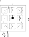
- FIG. 4B shows a conceptual illustration of a top-view of the fourth MTJ element 400 of FIG. 4A .
- MTJ element 400 includes tunnel barriers 430, 432, 434, and 435-438, each one of which may be substantially similar to tunnel barrier 108 of FIG. 1 .
- each one of tunnel barriers 430, 432, 434, and 435-438 may include a corresponding pinned layer and bottom electrode.
- each tunnel barrier of tunnel barriers 430, 432, 434, and 435-438 may be arranged above a respective pinned layer.
- tunnel barriers 408, 430, 432, 434, and 435-438 are arranged relative to free layer 404 to detect a circular motion 460.
- tunnel barriers 430, 432, 434, and 435-438 may be arranged relative to free layer 404 to detect ovoid motion.
- tunnel barriers 430, 432, 434, and 435-438 may be arranged relative to free layer 404 to detect quasi-circular motion.
- tunnel barrier 430 is arranged right of free layer 404 along first horizontal direction 442.
- tunnel barrier 432 is arranged left of free layer 404 along first horizontal direction 442.
- tunnel barrier 408 is arranged below free layer 404 along second horizontal direction 444.
- tunnel barrier 434 is arranged above free layer 404 along second horizontal direction 444.
- tunnel barrier 435 is arranged left of free layer 404 along first horizontal direction 442 and above free layer 404 along second horizontal direction 444.
- Tunnel barrier 436 may be arranged right of free layer 404 along first horizontal direction 442 and above free layer 404 along second horizontal direction 444.
- Tunnel barrier 437 is arranged left of free layer 404 along first horizontal direction 442 and below free layer 404 along second horizontal direction 444.
- Tunnel barrier 438 is arranged right of free layer 404 along first horizontal direction 442 and below free layer 404 along second horizontal direction 444.
- FIG. 5A shows a conceptual illustration of a cross-sectional view of a fifth MTJ element 500 configured to detect gyroscopic motion.
- MTJ element 500 may include support structure 502, free layer 504, magnetized portion 506, tunnel barrier 508, pinned layer 510, bottom electrode 512, base layer 514, substrate 516, metal 518, and via 520, which may be examples of support structure 102, free layer 104, magnetized portion 106, tunnel barrier 108, pinned layer 110, bottom electrode 112, base layer 114, substrate 116, metal 118, and via 120 of FIG. 1 , respectively.
- support structure 502 is arranged left of tunnel barrier 508 along first horizontal direction 542.
- FIG. 5B shows a conceptual illustration of a top-view of the fifth MTJ element 500 of FIG. 5A .
- fifth MTJ element 500 includes tunnel barriers 530, 532, and 534, each one of which may be substantially similar to tunnel barrier 508.
- each one of tunnel barriers 530, 532, and 534 may include a corresponding pinned layer and bottom electrode.
- each tunnel barrier of tunnel barriers 530, 532, and 534 may be arranged above a respective pinned layer.
- tunnel barriers 508, 530, 532, and 534 (and respective pinned layers) are arranged relative to free layer 504 to detect a square motion 560.
- tunnel barriers 508, 530, 532, and 534 (and respective pinned layers) may be arranged relative to free layer 504 to detect a rectangular motion.
- tunnel barrier 530 is arranged right of free layer 504 along first horizontal direction 542.
- tunnel barrier 532 is arranged left of free layer 504 along first horizontal direction 542.
- tunnel barrier 508 is arranged below free layer 504 along second horizontal direction 544.
- tunnel barrier 534 is arranged above free layer 504 along second horizontal direction 544.
- FIG. 6A shows a conceptual illustration of a cross-sectional view of a sixth MTJ element 600 configured to detect gyroscopic motion.
- MTJ element 600 may include support structure 602, free layer 604, magnetized portion 606, tunnel barrier 608, pinned layer 610, bottom electrode 612, base layer 614, substrate 616, metal 618, and via 620, which may be examples of support structure 102, free layer 104, magnetized portion 106, tunnel barrier 108, pinned layer 110, bottom electrode 112, base layer 114, substrate 116, metal 118, and via 120 of FIG. 1 , respectively.
- support structure 602 is arranged left of tunnel barrier 608 along first horizontal direction 642.
- FIG. 6B shows a conceptual illustration of a top-view of the sixth MTJ element 600 of FIG. 6A .
- MTJ element 600 includes tunnel barriers 630, 632, 634, and 635-638, each one of which may be substantially similar to tunnel barrier 108 of FIG. 1 .
- each one of tunnel barriers 630, 632, 634, and 635-638 may include a corresponding pinned layer and bottom electrode.
- each tunnel barrier of tunnel barriers 630, 632, 634, and 635-638 may be arranged above a respective pinned layer.
- tunnel barriers 608, 630, 632, 634, and 635-638 are arranged relative to free layer 604 to detect a circular motion 660.
- tunnel barriers 630, 636, 634, and 635-638 may be arranged relative to free layer 604 to detect ovoid motion.
- tunnel barriers 630, 632, 634, and 635-638 may be arranged relative to free layer 604 to detect quasi-circular motion.
- tunnel barrier 630 is arranged right of free layer 604 along first horizontal direction 642.
- tunnel barrier 632 is arranged left of free layer 604 along first horizontal direction 642.
- tunnel barrier 608 is arranged below free layer 604 along second horizontal direction 644.
- tunnel barrier 634 is arranged above free layer 604 along second horizontal direction 644.
- tunnel barrier 635 is arranged left of free layer 604 along first horizontal direction 642 and above free layer 604 along second horizontal direction 644.
- Tunnel barrier 636 may be arranged right of free layer 604 along first horizontal direction 642 and above free layer 604 along second horizontal direction 644.
- Tunnel barrier 637 is arranged left of free layer 604 along first horizontal direction 642 and below free layer 604 along second horizontal direction 644.
- Tunnel barrier 638 is arranged right of free layer 604 along first horizontal direction 642 and below free layer 604 along second horizontal direction 644.
- FIG. 7A shows a conceptual illustration of a cross-sectional view of a seventh MTJ element 700 configured to detect gyroscopic motion.
- MTJ element 700 may include support structure 702, free layer 704, magnetized portion 706, tunnel barrier 708, pinned layer 710, bottom electrode 712, base layer 714, substrate 716, metal 718, and via 720, which may be examples of support structure 102, free layer 104, magnetized portion 106, tunnel barrier 108, pinned layer 110, bottom electrode 112, base layer 114, substrate 116, metal 118, and via 120 of FIG. 1 , respectively.
- free layer 704 is spaced next to tunnel barrier 708 along vertical direction 740.
- magnetized portion 706 is spaced next to tunnel barrier 708 along vertical direction 740.
- magnetized portion 706 may be arranged above pinned layer 710 and coplanar with tunnel barrier 708.
- support structure 702 is arranged left of tunnel barrier 708 along first horizontal direction 742.
- FIG. 7B shows a conceptual illustration of a top-view of the seventh MTJ element 700 of FIG. 7A .
- seventh MTJ element 700 includes tunnel barriers 730, 732, and 734, each one of which may be substantially similar to tunnel barrier 708.
- each one of tunnel barriers 730, 732, and 734 may include a corresponding pinned layer and bottom electrode.
- each tunnel barrier of tunnel barriers 730, 732, and 734 may be arranged above a respective pinned layer.
- tunnel barriers 708, 730, 732, and 734 (and respective pinned layers) are arranged relative to free layer 704 to detect a square motion 760.
- tunnel barriers 708, 730, 732, and 734 (and respective pinned layers) may be arranged relative to free layer 704 to detect a rectangular motion.
- tunnel barrier 730 is arranged right of free layer 704 along first horizontal direction 742.
- tunnel barrier 732 is arranged left of free layer 704 along first horizontal direction 742.
- tunnel barrier 708 is arranged below free layer 704 along second horizontal direction 744.
- tunnel barrier 734 is arranged above free layer 704 along second horizontal direction 744.
- FIG. 8A shows a conceptual illustration of a cross-sectional view of an eighth MTJ element 800 configured to detect gyroscopic motion.
- MTJ element 800 may include support structure 802, free layer 804, magnetized portion 806, tunnel barrier 808, pinned layer 810, bottom electrode 812, base layer 814, substrate 816, metal 818, and via 820, which may be examples of support structure 102, free layer 104, magnetized portion 106, tunnel barrier 108, pinned layer 110, bottom electrode 112, base layer 114, substrate 116, metal 118, and via 120 of FIG. 1 , respectively.
- free layer 804 is spaced next to tunnel barrier 808 along vertical direction 840.
- magnetized portion 806 may be arranged above pinned layer 810 and coplanar with tunnel barrier 808. In some examples, magnetized portion 806 is spaced next to tunnel barrier 808 along vertical direction 840. In the example of FIG. 8A , support structure 802 is arranged left of tunnel barrier 808 along first horizontal direction 842.
- FIG. 8B shows a conceptual illustration of a top-view of the eighth MTJ element 800 of FIG. 8A .
- eighth MTJ element 800 includes tunnel barriers 830, 832, 834, and 835-838, each one of which may be substantially similar to tunnel barrier 108 of FIG. 1 .
- each one of tunnel barriers 830, 832, 834, and 835-838 may include a corresponding pinned layer and bottom electrode.
- each tunnel barrier of tunnel barriers 830, 832, 834, and 835-838 may be arranged above a respective pinned layer.
- tunnel barriers 808, 830, 832, 834, and 835-838 are arranged relative to free layer 804 to detect a circular motion 860.
- tunnel barriers 830, 838, 834, and 835-838 may be arranged relative to free layer 804 to detect ovoid motion.
- tunnel barriers 830, 832, 834, and 835-838 may be arranged relative to free layer 804 to detect quasi-circular motion.
- tunnel barrier 830 is arranged right of free layer 804 along first horizontal direction 842.
- tunnel barrier 832 is arranged left of free layer 804 along first horizontal direction 842.
- tunnel barrier 808 is arranged below free layer 804 along second horizontal direction 844.
- tunnel barrier 834 is arranged above free layer 804 along second horizontal direction 844.
- tunnel barrier 835 is arranged left of free layer 804 along first horizontal direction 842 and above free layer 804 along second horizontal direction 844.
- Tunnel barrier 836 may be arranged right of free layer 804 along first horizontal direction 842 and above free layer 804 along second horizontal direction 844.
- Tunnel barrier 837 is arranged left of free layer 804 along first horizontal direction 842 and below free layer 804 along second horizontal direction 844.
- Tunnel barrier 838 is arranged right of free layer 804 along first horizontal direction 842 and below free layer 804 along second horizontal direction 844.
- FIG. 9A shows a conceptual illustration of a cross-sectional view of a ninth MTJ element 900 configured to detect gyroscopic motion.
- MTJ element 900 may include free layer 904, magnetized portion 906, tunnel barrier 908, pinned layer 910, bottom electrode 912, base layer 914, and substrate 916, which may be examples of free layer 104, magnetized portion 106, tunnel barrier 108, pinned layer 110, bottom electrode 112, base layer 114, and substrate 116 of FIG. 1 , respectively.
- free layer 904 extends from base layer 914 along vertical direction 940.
- pinned layer 910 is arranged above base layer 914 and free layer 904 extends along vertical direction 940 away from base layer 914.
- free layer 904 includes magnetized portion 906 arranged above pinned layer 910 and coplanar with tunnel barrier 908.
- FIG. 9B shows a conceptual illustration of a top-view of the ninth MTJ element 900 of FIG. 9A .
- MTJ element 900 includes tunnel barriers 930, 932, and 934, each one of which may be substantially similar to tunnel barrier 908.
- each one of tunnel barriers 930, 932, and 934 may include a corresponding pinned layer and bottom electrode.
- each tunnel barrier of tunnel barriers 930, 932, and 934 may be arranged above a respective pinned layer.
- tunnel barriers 908, 930, 932, and 934 (and respective pinned layers) are arranged relative to free layer 904 to detect a square motion 960.
- tunnel barriers 908, 930, 932, and 934 (and respective pinned layers) may be arranged relative to free layer 904 to detect a rectangular motion.
- tunnel barrier 930 is arranged right of free layer 904 along first horizontal direction 942.
- tunnel barrier 932 is arranged left of free layer 904 along first horizontal direction 942.
- tunnel barrier 908 is arranged below free layer 904 along second horizontal direction 944.
- tunnel barrier 934 is arranged above free layer 904 along second horizontal direction 944.
- FIG. 10A shows a conceptual illustration of a cross-sectional view of a tenth MTJ element 1000 configured to detect gyroscopic motion.
- MTJ element 1000 may include free layer 1004, magnetized portion 1006, tunnel barrier 1008, pinned layer 1010, bottom electrode 1012, base layer 1014, and substrate 1016, which may be examples of free layer 104, magnetized portion 106, tunnel barrier 108, pinned layer 110, bottom electrode 112, base layer 114, and substrate 116 of FIG. 1 , respectively.
- free layer 1004 extends from base layer 1014 along vertical direction 1040.
- pinned layer 1010 is arranged above base layer 1014 and free layer 1004 extends along vertical direction 1040 away from base layer 1014.
- free layer 1004 includes magnetized portion 1006 arranged above pinned layer 1010 and coplanar with tunnel barrier 1008.
- FIG. 10B shows a conceptual illustration of a top-view of the tenth MTJ element 1000 of FIG. 10A .
- MTJ element 1000 includes tunnel barriers 1030, 1032, 1034, and 1035-1038, each one of which may be substantially similar to tunnel barrier 108 of FIG. 1 .
- each one of tunnel barriers 1030, 1032, 1034, and 1035-1038 may include a corresponding pinned layer and bottom electrode.
- each tunnel barrier of tunnel barriers 1030, 1032, 1034, and 1035-1038 (and respective pinned layers) may be arranged above a respective pinned layer.
- tunnel barriers 1008, 1030, 1032, 1034, and 1035-1038 are arranged relative to free layer 1004 to detect a circular motion 1060.
- tunnel barriers 1030, 1038, 1034, and 1035-1038 (and respective pinned layers) may be arranged relative to free layer 1004 to detect ovoid motion.
- tunnel barriers 1030, 1032, 1034, and 1035-1038 may be arranged relative to free layer 1004 to detect quasi-circular motion.
- tunnel barrier 1030 is arranged right of free layer 1004 along first horizontal direction 1042.
- tunnel barrier 1032 is arranged left of free layer 1004 along first horizontal direction 1042.
- tunnel barrier 1008 is arranged below free layer 1004 along second horizontal direction 1044.
- tunnel barrier 1034 is arranged above free layer 1004 along second horizontal direction 1044.
- tunnel barrier 1035 is arranged left of free layer 1004 along first horizontal direction 1042 and above free layer 1004 along second horizontal direction 1044.
- Tunnel barrier 1036 may be arranged right of free layer 1004 along first horizontal direction 1042 and above free layer 1004 along second horizontal direction 1044.
- Tunnel barrier 1037 is arranged left of free layer 1004 along first horizontal direction 1042 and below free layer 1004 along second horizontal direction 1044.
- Tunnel barrier 1038 is arranged right of free layer 1004 along first horizontal direction 1042 and below free layer 1004 along second horizontal direction 1044.
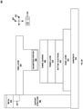
- FIG. 11 shows a conceptual illustration of a first gyroscopic sensor device 1100 that may be used to implement the techniques of the present disclosure.
- Gyroscopic sensor device 1100 may include support structure 1102, bottom electrode 1112, base layer 1114, processing circuity 1116, metal 1118, and via 1120, which may be examples of support structure 102, bottom electrode 112, base layer 114, substrate 116, metal 118, and via 120 of FIG. 1 , respectively.
- Gyroscopic sensor device 1100 may further include sensor module 1103, which may comprise a free layer, one or more tunnel barriers, and one or more pinned layers arranged for detecting gyroscopic motion using a support structure (e.g., see FIGS.
- FIG. 11 illustrates a single bottom electrode, some examples, may include two or more (e.g., 4, 8, etc.) bottom electrodes that are each connected to a respective pinned layer and a respective tunnel barrier.
- Sensor devices implementing one or more of the techniques described in this disclosure may be implemented in a wide array of electronic devices ranging from small portable devices such as music players, smart phones, game cartridges, and memory sticks up to larger devices such as tablet computers, gaming devices or consoles, desktop computers, super computers, and enterprise storage solutions.
- Support structure 1102 may include via 1150 adapted to electrically couple a free layer of sensor module 1103 to processing circuitry 1116.
- Via 1150 and via 1152 may be formed of an electrically conductive material, such as, for example, but not limited to, tungsten, aluminum, aluminum-copper, and/or copper.
- via 1150 electrically connects metal 1118 to processing circuity 1116.
- via 1152 electrically connects bottom electrode 1112 to processing circuity 1116.
- Processing circuitry 1116 is configured to monitor the resistance(s) and/or magnetoresistance(s) of sensor module 1103, which may correspond to gyroscopic motion of gyroscopic sensor device 1100. This monitoring of the resistance(s) and/or magnetoresistance(s) is termed Rmonitor, which represents the real time measuring of the MTJ element resistance(s) and/or magnetoresistance(s). For example, processing circuitry 1116 may determine an angular velocity is increasing as a magnitude of resistance and/or magnetoresistance between a free layer and a particular pinned layer of sensor module 1103 decreases.
- Processing circuitry 1116 may be adapted to compare two or more respective resistances between each pinned layer and the free layer to determine gyroscopic motion. For example, processing circuitry 1116 may compare a first resistance between a respective pinned layer for tunnel barrier 130 and free layer 104 to a second resistance between a respective pinned layer for tunnel barrier 132 and free layer 104 to determine gyroscopic motion along first horizontal direction 142. In some examples, processing circuitry 1116 may compare a third resistance between a respective pinned layer for tunnel barrier 108 and free layer 104 to a fourth resistance between a respective pinned layer for tunnel barrier 134 and free layer 104 to determine gyroscopic motion along second horizontal direction 144.
- Processing circuitry 1116 may be adapted to determine gyroscopic motion has occurred along first horizontal direction 142. For example, processing circuitry 1116 may determine gyroscopic motion has occurred along first horizontal direction 142 when a first resistance between a respective pinned layer for tunnel barrier 130 and free layer 104 is greater than a second resistance between a respective pinned layer for tunnel barrier 132 and free layer 104. Similarly, processing circuitry 1116 may determine gyroscopic motion has occurred along first horizontal direction 142 when a first resistance between a respective pinned layer for tunnel barrier 130 and free layer 104 is less than a second resistance between a respective pinned layer for tunnel barrier 132 and free layer 104.
- Processing circuitry 1116 may be adapted to determine gyroscopic motion has occurred along second horizontal direction 144. For example, processing circuitry 1116 may determine gyroscopic motion has occurred along second horizontal direction 144 when a third resistance between a respective pinned layer for tunnel barrier 108 and free layer 104 is greater than a fourth resistance between a respective pinned layer for tunnel barrier 134 and free layer 104 to determine gyroscopic motion along second horizontal direction 144.
- processing circuitry 1116 may determine gyroscopic motion has occurred along second horizontal direction 144 when a third resistance between a respective pinned layer for tunnel barrier 108 and free layer 104 is less than a fourth resistance between a respective pinned layer for tunnel barrier 134 and free layer 104 to determine gyroscopic motion along second horizontal direction 144.
- Processing circuitry 1116 may be adapted to output an indication of the gyroscopic motion. For example, processing circuitry 1116 may generate a digital signal indicating gyroscopic motion along first horizonal direction 142 and/or second horizonal direction 144. In some examples, processing circuitry 1116 may generate one or more voltages magnitudes indicating gyroscopic motion along first horizonal direction 142 and/or second horizonal direction 144.
- Processing circuitry 1116 may include one or more processors, including one or more microprocessors, digital signal processors (DSPs), ASICs, field programmable gate arrays (FPGAs), or any other equivalent integrated or discrete logic circuitry, as well as any combinations of such components.
- DSPs digital signal processors
- FPGAs field programmable gate arrays
- the term "processor” or “processing circuitry” may generally refer to any of the foregoing logic circuitry, alone or in combination with other logic circuitry, or any other equivalent circuitry.
- MTJ element 100 of FIGS. 1A-1D other examples may use other MTJ elements (e.g., 2A-2B, 3A-3B, 4A-4B. 5A-5B, 6A-6B, 7A-7B, 8A-8B, etc.)
- FIG. 12 shows a conceptual illustration of a second gyroscopic sensor device 1200 that may be used to implement the techniques of the present disclosure.
- Gyroscopic sensor device 1200 may include bottom electrode 1212, base layer 1214, and processing circuity 1216, which may be examples of bottom electrode 112, base layer 114, and substrate 116 of FIG. 1 , respectively.
- Gyroscopic sensor device 1200 may further include sensor module 1203, which may comprise a free layer, one or more tunnel barriers, and one or more pinned layers arranged for detecting gyroscopic motion (e.g., see FIGS. 9A-9B , and 10A-10B ).
- FIG. 12 illustrates a single bottom electrode, some examples, may include two or more (e.g., 4, 8, etc.) bottom electrodes that are each connected to a respective pinned layer and a respective tunnel barrier.
- Sensor devices implementing one or more of the techniques described in this disclosure may be implemented in a wide array of electronic devices ranging from small portable devices such as music players, smart phones, game cartridges, and memory sticks up to larger devices such as tablet computers, gaming devices or consoles, desktop computers, super computers, and enterprise storage solutions.
- base layer 1214 comprises via 1250 adapted to electrically couple a free layer of sensor module 1203 to processing circuitry 1216.
- Via 1250 and via 1252 may be formed of an electrically conductive material, such as, for example, but not limited to, copper.
- via 1250 electrically connects a free layer of sensor module 1203 to processing circuity 1216.
- via 1252 electrically connects bottom electrode 1212 to processing circuity 1216.
- Processing circuitry 1216 is configured to monitor the resistance(s) and/or magnetoresistance(s) of sensor module 1203, which may correspond to gyroscopic motion of gyroscopic sensor device 1200. This monitoring of the resistance(s) and/or magnetoresistance(s) is termed Rmonitor, which represents the real time measuring of the MTJ element resistance(s) and/or magnetoresistance(s). For example, processing circuitry 1216 may determine an angular velocity is increasing as a magnitude of resistance and/or magnetoresistance between a free layer and a particular tunnel barrier of sensor module 1203 decreases.
- Processing circuitry 1216 may be adapted to compare two or more respective resistances between each pinned layer and the free layer to determine gyroscopic motion. For example, processing circuitry 1216 may compare a first resistance between a respective pinned layer for tunnel barrier 930 and free layer 904 to a second resistance between a respective pinned layer for tunnel barrier 932 and free layer 904 to determine gyroscopic motion along first horizontal direction 942. In some examples, processing circuitry 1216 may compare a third resistance between a respective pinned layer for tunnel barrier 908 and free layer 904 to a fourth resistance between a respective pinned layer for tunnel barrier 934 and free layer 904 to determine gyroscopic motion along second horizontal direction 944.
- Processing circuitry 1216 may be adapted to determine gyroscopic motion has occurred along first horizontal direction 942. For example, processing circuitry 1216 may determine gyroscopic motion has occurred along first horizontal direction 942 when a first resistance between a respective pinned layer for tunnel barrier 930 and free layer 904 is greater than a second resistance between a respective pinned layer for tunnel barrier 932 and free layer 904. Similarly, processing circuitry 1216 may determine gyroscopic motion has occurred along first horizontal direction 942 when a first resistance between a respective pinned layer for tunnel barrier 930 and free layer 904 is less than a second resistance between a respective pinned layer for tunnel barrier 932 and free layer 904.
- Processing circuitry 1216 may be adapted to determine gyroscopic motion has occurred along second horizontal direction 944. For example, processing circuitry 1216 may determine gyroscopic motion has occurred along second horizontal direction 944 when a third resistance between a respective pinned layer for tunnel barrier 908 and free layer 904 is greater than a fourth resistance between a respective pinned layer for tunnel barrier 934 and free layer 904 to determine gyroscopic motion along second horizontal direction 944.
- processing circuitry 1216 may determine gyroscopic motion has occurred along second horizontal direction 944 when a third resistance between a respective pinned layer for tunnel barrier 908 and free layer 904 is less than a fourth resistance between a respective pinned layer for tunnel barrier 934 and free layer 904 to determine gyroscopic motion along second horizontal direction 944.
- Processing circuitry 1216 may be adapted to output an indication of the gyroscopic motion. For example, processing circuitry 1216 may generate a digital signal indicating gyroscopic motion along first horizonal direction 942 and/or second horizonal direction 944. In some examples, processing circuitry 1216 may generate one or more voltages magnitudes indicating gyroscopic motion along first horizonal direction 942 and/or second horizonal direction 944.
- Processing circuitry 1216 may include one or more processors, including one or more microprocessors, digital signal processors (DSPs), ASICs, field programmable gate arrays (FPGAs), or any other equivalent integrated or discrete logic circuitry, as well as any combinations of such components.
- DSPs digital signal processors
- FPGAs field programmable gate arrays
- FIGS. 1A-1D other examples may use other MTJ elements (e.g., 2A-2B, 3A-3B, 4A-4B. 5A-5B, 6A-6B, 7A-7B, 8A-8B, etc.)
- FIG. 13 shows a flowchart of operations for detecting gyroscopic motion in accordance with the techniques of this disclosure.
- the operations of FIG. 13 may, for example, be performed by a MTJ element described above with respect to any combination of FIGS. 1A-1D , 2A-2B , 3A-3B , 4A-4B . 5A-5B , 6A-6B , 7A-7B , 8A-8B , 9A-9B , 10A-10B , 11 , and 12 .
- Processing circuitry 1116 and/or processing circuitry 1216 measures a resistance at a MTJ element (1302).
- Processing circuitry 1116 and/or processing circuitry 1216 determines gyroscopic motion based on the resistance at the MTJ element (1304).
- processing circuitry 1116 and/or processing circuitry 1216 determines gyroscopic motion based on a resistance at sensor module 1103 and/or sensor module 1203.
- Processing circuitry 1116 and/or processing circuitry 1216 outputs an indication of the gyroscopic motion (1306).
- circuitry may refer to any of the foregoing structure or any other structure suitable for processing program code and/or data or otherwise implementing the techniques described herein.
- Circuitry may, for example, any of a variety of types of solid state circuit elements, such as CPUs, CPU cores, GPUs, DSPs, ASICs, mixed-signal integrated circuits, FPGAs, microcontrollers, programmable logic controllers (PLCs), programmable logic device (PLDs), complex PLDs (CPLDs), systems on a chip (SoC), any subsection of any of the above, an interconnected or distributed combination of any of the above, or any other integrated or discrete logic circuitry, or any other type of component or one or more components capable of being configured in accordance with any of the examples disclosed herein.
- PLCs programmable logic controllers
- PLDs programmable logic device
- SoC systems on a chip
- circuitry may also include one or more memory devices, such as any volatile or non-volatile media, such as a RAM, ROM, non-volatile RAM (NVRAM), electrically erasable programmable ROM (EEPROM), flash memory, and the like.
- the one or more memory devices may store computer-readable instructions that, when executed or processed the circuitry, cause the circuitry to implement the techniques attributed herein to circuitry.
- the circuitry of this disclosure may be programmed, or otherwise controlled, with various forms of firmware and/or software.
Landscapes
- Engineering & Computer Science (AREA)
- Signal Processing (AREA)
- Physics & Mathematics (AREA)
- General Physics & Mathematics (AREA)
- Radar, Positioning & Navigation (AREA)
- Remote Sensing (AREA)
- Chemical & Material Sciences (AREA)
- Crystallography & Structural Chemistry (AREA)
- Power Engineering (AREA)
- Hall/Mr Elements (AREA)
Description
- This disclosure relates to sensor devices and, more specifically, to spintronic-based devices that are configured to detect gyroscopic motion.
- Some devices include a gyroscopic sensor device that monitors gyroscopic motion of a device. It is desirable for such devices to detect gyroscopic motion of the device to provide context of the device. For example, a position of the device may be controlled based on the gyroscopic motion of the device. It is generally desirable for a gyroscopic sensor device to measure accurately gyroscopic motion and to operate in a smaller space. Current types of gyroscopic sensor devices include non-magnetic sensors that generate a voltage in response changes in angular velocity of the device.
US5859368 discloses a tunnelling-based rotation rate sensor.US5905202 discloses a tunnelling rotation sensor.CN104567848 discloses a micromechanical gyroscope based on the tunnel magnetoresistive effect.CN102853826 discloses a silicon based tunneling magnetoresistance micro gyroscope.CN105180914 discloses an in-plane detection micromechanical gyroscope. - This disclosure generally describes techniques for detecting gyroscopic motion using a spintronic-based sensor device. The techniques may in some instances provide for a higher density for a smaller and more lightweight form factor. Furthermore, a spintronic-based sensor device may be more resistive to ElectroMagnetic Interference (EMI) than non-magnetic sensors, which may be of particular benefit to certain applications.
- The invention includes a magnetic tunnel junction (MTJ) based sensor device according to claim 1 and a method for detecting gyroscopic motion using a MTJ based sensor device according to claim 16.
- The details of one or more aspects of the disclosure are set forth in the accompanying drawings and the description below. Other features, objects, and advantages of the devices, systems, methods, and techniques described in this disclosure will be apparent from the description and drawings, and from the claims.
-
-
FIG. 1A shows a conceptual illustration of a cross-sectional view of a first magnetic tunnel junction (MTJ) element configured to gyroscopic motion. -
FIG. 1B shows a conceptual illustration of a top-view of the first MTJ element ofFIG. 1A . -
FIG. 1C shows a conceptual illustration of a cross-sectional view of the first MTJ element ofFIG. 1A during a first angular velocity. - FIG. ID shows a conceptual illustration of a cross-sectional view of the first MTJ element of
FIG. 1A during a second angular velocity. -
FIG. 2A shows a conceptual illustration of a cross-sectional view of a second MTJ element configured to detect gyroscopic motion. -
FIG. 2B shows a conceptual illustration of a top-view of the second MTJ element ofFIG. 2A . -
FIG. 3A shows a conceptual illustration of a cross-sectional view of a third MTJ element configured to detect gyroscopic motion. -
FIG. 3B shows a conceptual illustration of a top-view of the third MTJ element ofFIG. 3A . -
FIG. 4A shows a conceptual illustration of a cross-sectional view of a fourth MTJ element configured to detect gyroscopic motion. -
FIG. 4B shows a conceptual illustration of a top-view of the fourth MTJ element ofFIG. 4A . -
FIG. 5A shows a conceptual illustration of a cross-sectional view of a fifth MTJ element configured to detect gyroscopic motion. -
FIG. 5B shows a conceptual illustration of a top-view of the fifth MTJ element ofFIG. 5A . -
FIG. 6A shows a conceptual illustration of a cross-sectional view of a sixth MTJ element configured to detect gyroscopic motion. -
FIG. 6B shows a conceptual illustration of a top-view of the sixth MTJ element ofFIG. 6A . -
FIG. 7A shows a conceptual illustration of a cross-sectional view of a seventh MTJ element configured to detect gyroscopic motion. -
FIG. 7B shows a conceptual illustration of a top-view of the seventh MTJ element ofFIG. 7A . -
FIG. 8A shows a conceptual illustration of a cross-sectional view of an eighth MTJ element configured to detect gyroscopic motion. -
FIG. 8B shows a conceptual illustration of a top-view of the eighth MTJ element ofFIG. 8A . -
FIG. 9A shows a conceptual illustration of a cross-sectional view of a ninth MTJ element configured to detect gyroscopic motion. -
FIG. 9B shows a conceptual illustration of a top-view of the ninth MTJ element ofFIG. 9A . -
FIG. 10A shows a conceptual illustration of a cross-sectional view of a tenth MTJ element configured to detect gyroscopic motion. -
FIG. 10B shows a conceptual illustration of a top-view of the tenth MTJ element ofFIG. 10A . -
FIG. 11 shows a conceptual illustration of a first gyroscopic sensor device that may be used to implement the techniques of the present disclosure. -
FIG. 12 shows a conceptual illustration of a second gyroscopic sensor device that may be used to implement the techniques of the present disclosure. -
FIG. 13 shows a flowchart of operations for detecting gyroscopic motion in accordance with the techniques of this disclosure. - Some applications have been identified in which miniaturized sensing devices are needed for operation in unique environments. Such sensing devices may be configurable for strategic applications. For example, such sensing devices may be radiation-hardened, and to include magnetically-based devices that can be integrated (e.g., monolithically, in particular initially) into a compact module with Application-Specific Integrated Circuits (ASICs) including those that contain embedded Magnetoresistive Random Access Memory (MRAM) bits. Of various sensing devices of interest, one device of interest that is discussed here is a gyroscope sensor device that could be used with or separately from other sensors (e.g., an acceleration sensor, a mechanical shock and vibration sensor, etc.), and that may support compatibility with MRAM technology.
- In accordance with one or more techniques described herein, circuitry may be constructed to include a magnetic tunnel junction (MTJ), which is an example of a spintronic device, with desired, resistance, resistance-area product, and dimensions. Examples of resistance and/or magnetoresistance may include, but are not limited to, tunnel magnetoresistance (TMR), giant magnetoresistance (GMR), anisotropic magnetoresistive (AMR), and other resistance and/or magnetoresistance effects.
- Within a tunnel barrier structure between two magnetic layers of the MTJ, techniques described herein may include one or more test structure(s) such as rectangular, square, circular, ovoid, or quasi-circular shape(s) with designed symmetries and/or asymmetries and placed in a circular or similar arrangement, that can be tethered/suspended to respond to pivoting and/or torsional displacements and rotations. The test structure(s) can be constructed from and/or coated with a magnetic material that may be patterned. Processing circuitry may make use electrical, electronic, or spintronic current(s). Tunneling current(s) can be spin-dependent or spin-independent, and ballistic electron tunneling may be used. Anisotropic, Giant, and/or Tunneling Magneto-Resistive effects may be used for sensing gyroscope motion.
- For example, a free layer may flex towards and/or away from each one of a plurality of pinned layers. Such flexing by the free layer may cause corresponding changes in resistance of the MTJ formed by the free layer and each one of the plurality of pinned layers. In this way, processing circuitry may detect gyroscopic motion using the resistance of the MTJ.
- Such magnetic/spintronic devices may provide unique and desired application functionality, customization prospects, and environmental capability (e.g., shock, vibration, radiation, acceleration, motion) for various environments. Such magnetic/spintronic devices may offer materials and technological similarity and compatibility with MRAM bits and other sensing devices such as accelerometers, gyros, and pressure sensors, which may support integration, modularity, miniaturization, and packaging with embedded MRAM and ASICS. In some examples, the spintronic-based gyroscopic sensor device described herein may be used for die-to-die or monolithic integration with MTJs/MTJ die.
-
FIG. 1A shows a conceptual illustration of a cross-sectional view of a first magnetic tunnel junction (MTJ)element 100 configured to gyroscopic motion.MTJ element 100 may includesupport structure 102,free layer 104,tunnel barrier 108, pinnedlayer 110,bottom electrode 112,base layer 114, andsubstrate 116. As shown inFIG. 1A ,support structure 102 extends fromsubstrate 116 alongvertical direction 140 and is spaced apart fromtunnel barrier 108 along firsthorizontal direction 142. Secondhorizontal direction 144 is perpendicular to firsthorizontal direction 142 andvertical direction 140. -
Base layer 114 may comprise, for example, silicon (Si).Substrate 116 may comprise, for example, silicon (Si). In some examples,substrate 116 may include processing circuitry. For example,substrate 116 may include metallization and/or integrated circuitry (e.g., Complementary metal-oxide-semiconductor (CMOS)). -
Support structure 102 may be adapted to arrangefree layer 104 abovetunnel barrier 108.Support structure 102 may be formed of silicon, silicon nitride, silicon oxide, copper, aluminum, aluminum oxide, magnesium oxide, or another material. As shown,support structure 102 may include via 120 andmetal 118. Via 120 andmetal 118 may be formed of a conductive material to permit a connection toMTJ element 100. Examples of conductive materials may include, but are not limited to, copper.Bottom electrode 112 may be formed of a conductive material to permit a connection toMTJ element 100. In the example ofFIG. 1A ,support structure 102 is arranged right oftunnel barrier 508 along firsthorizontal direction 142. In some examples,support structure 102 is arranged left oftunnel barrier 508 along firsthorizontal direction 142.Support structure 102 may be arranged above and/or belowtunnel barrier 108 along secondhorizontal direction 144. -
Free layer 104 may include a magnetization direction that is free to switch between a parallel orientation and an antiparallel orientation. As shown,free layer 104 may includemagnetized portion 106. In the example ofFIG. 1 ,magnetized portion 106 is arranged abovetunnel barrier 108.Magnetized portion 106 may include, for example, but not limited to, a metal and/or a metal/ferromagnetic metal system. For instance,magnetized portion 106 may be formed of a metal or metal/ferromagnetic metal system on Silicon Oxide (SiOx), Silicon Nitride (SiNx), and/or Silicon (Si). -
Tunnel barrier 108 includes a non-magnetic metal that separatesfree layer 104 and pinnedlayer 110. In some examples,tunnel barrier 108 may be formed of aluminum oxide, magnesium oxide, or another material. In the example ofFIG. 1A ,free layer 104 and/ormagnetized portion 106 is spaced apart fromtunnel barrier 108 alongvertical direction 140. For instance, a void may separatefree layer 104 andtunnel barrier 108. In some instances, a void may separatemagnetized portion 106 andtunnel barrier 108. In some examples, a bottom portion offree layer 104 may be adjacent to a top portion oftunnel barrier 108 alongvertical direction 140. In some examples,free layer 104 and/ormagnetized portion 106 is spaced next totunnel barrier 108 alongvertical direction 140. - Pinned
layer 110 includes a magnetization direction that is fixed or "pinned" to a single orientation. For example, pinnedlayer 110 may be pinned in a parallel orientation. In other examples, pinnedlayer 110 may be pinned in an antiparallel orientation. In the example ofFIG. 1A , pinnedlayer 110 includes an anti-ferromagnetic layer, such that the magnetization direction of the pinnedlayer 110 is "pinned" in a particular orientation. The magnetization direction of the pinnedlayer 110 remains relatively fixed when operational magnetic fields are applied toMTJ element 100. - In the example of
FIG. 1A ,MTJ element 100 may be formed as follows. Initially, material fortunnel barrier 108 and pinnedlayer 110 is deposited. An oxide is formed ontunnel barrier 108 andtunnel barrier 108 and pinnedlayer 110 are etched.Tunnel barrier 108 and pinnedlayer 110 are encapsulated (for spacing). Material for free layer 104 (which can be rectangular or triangular, e.g., in area) andsupport structure 102 are deposed (with a top electrode for connection to metallization). The encapsulating material is removed and/or dissolved. - In the example of
FIG. 1A , a magnetization direction offree layer 104 is used to detect a gyroscopic motion ofMTJ element 100. For example,portion 107 offree layer 104 may flex in response to gyroscopic motion, resulting in a corresponding change in resistance and/or magnetoresistance ofMTJ element 100. In this example, processing circuitry may detect gyroscopic motion using the resistance and/or magnetoresistance of theMTJ element 100. In this manner,MTJ element 100 may be used as a gyroscopic motion sensor. -
FIG. 1B shows a conceptual illustration of a top-view of thefirst MTJ element 100 ofFIG. 1A . In the example ofFIGS. 1A and1B ,first MTJ element 100 includestunnel barriers tunnel barrier 108. Although not shown, each one oftunnel barriers tunnel barriers tunnel barriers free layer 104 to detect asquare motion 160. In some examples,tunnel barriers free layer 104 to detect a rectangular motion. - As shown,
tunnel barrier 130 is arranged right offree layer 104 along firsthorizontal direction 142. In this example,tunnel barrier 132 is arranged left offree layer 104 along firsthorizontal direction 142. Said differently, for example,tunnel barrier 132 is arranged along firsthorizontal direction 142 on an opposite side offree layer 104 fromtunnel barrier 130. In this example,tunnel barrier 108 is arranged belowfree layer 104 along secondhorizontal direction 144. In this example,tunnel barrier 134 is arranged abovefree layer 104 along secondhorizontal direction 144. Said differently, for example,tunnel barrier 108 is arranged along secondhorizontal direction 144 on an opposite side offree layer 104 fromtunnel barrier 134. - As shown,
magnetized portion 106 is centered to be approximately equidistant fromtunnel barriers horizontal direction 142 and secondhorizontal direction 144. -
FIG. 1C shows a conceptual illustration of a cross-sectional view of thefirst MTJ element 100 ofFIG. 1A during first angular velocity 150. In the example ofFIG. 1C ,portion 107 offree layer 104 flexes towardtunnel barrier 108 along secondhorizontal direction 144 in response to first angular velocity 150. As such,magnetized portion 106 is arranged closer totunnel barrier 108 thantunnel barrier 134, which reduces a resistance and/or magnetoresistance betweenfree layer 104 and a pinned layer belowtunnel barrier 108. - FIG. ID shows a conceptual illustration of a cross-sectional view of the
first MTJ element 100 ofFIG. 1A during a secondangular velocity 152. In the example of FIG. ID,portion 107 offree layer 104 flexes towardtunnel barrier 130 along firsthorizontal direction 142 in response to secondangular velocity 152. As such,magnetized portion 106 is arranged closer totunnel barrier 130 thantunnel barrier 132, which reduces a resistance and/or magnetoresistance betweenfree layer 104 and a pinned layer belowtunnel barrier 134. -
FIG. 2A shows a conceptual illustration of a cross-sectional view of asecond MTJ element 200 configured to detect gyroscopic motion.MTJ element 200 may includesupport structure 202,free layer 204,magnetized portion 206,tunnel barrier 208, pinnedlayer 210,bottom electrode 212,base layer 214,substrate 216,metal 218, and via 220, which may be examples ofsupport structure 102,free layer 104,magnetized portion 106,tunnel barrier 108, pinnedlayer 110,bottom electrode 112,base layer 114,substrate 116,metal 118, and via 120 ofFIG. 1 , respectively. -
FIG. 2B shows a conceptual illustration of a top-view of thesecond MTJ element 200 ofFIG. 2A . In the example ofFIGS. 2A and2B ,second MTJ element 200 includestunnel barriers tunnel barrier 108 ofFIG. 1 . Although not shown, each one oftunnel barriers tunnel barriers tunnel barriers free layer 204 to detect acircular motion 260. In some examples,tunnel barriers free layer 204 to detect ovoid motion. In some examples,tunnel barriers free layer 204 to detect quasi-circular motion. - In the example of
FIGS. 2A and2B ,tunnel barrier 230 is arranged right offree layer 204 along firsthorizontal direction 242. In this example,tunnel barrier 232 is arranged left offree layer 204 along firsthorizontal direction 242. Said differently, for example,tunnel barrier 232 is arranged along firsthorizontal direction 242 on an opposite side offree layer 204 fromtunnel barrier 230. In this example,tunnel barrier 208 is arranged belowfree layer 204 along secondhorizontal direction 244. In this example,tunnel barrier 234 is arranged abovefree layer 204 along secondhorizontal direction 244. Said differently, for example,tunnel barrier 208 is arranged along secondhorizontal direction 244 on an opposite side offree layer 204 fromtunnel barrier 234. - Further, as shown,
tunnel barrier 235 is arranged left offree layer 204 along firsthorizontal direction 242 and abovefree layer 204 along secondhorizontal direction 244.Tunnel barrier 236 may be arranged right offree layer 204 along firsthorizontal direction 242 and abovefree layer 204 along secondhorizontal direction 244.Tunnel barrier 237 is arranged left offree layer 204 along firsthorizontal direction 242 and belowfree layer 204 along secondhorizontal direction 244.Tunnel barrier 238 is arranged right offree layer 204 along firsthorizontal direction 242 and belowfree layer 204 along secondhorizontal direction 244. -
FIG. 3A shows a conceptual illustration of a cross-sectional view of athird MTJ element 300 configured to detect gyroscopic motion.MTJ element 300 may includesupport structure 302,free layer 304,magnetized portion 306,tunnel barrier 308, pinnedlayer 310,bottom electrode 312,base layer 314,substrate 316,metal 318, and via 320, which may be examples ofsupport structure 102,free layer 104,magnetized portion 106,tunnel barrier 108, pinnedlayer 110,bottom electrode 112,base layer 114,substrate 116,metal 118, and via 120 ofFIG. 1 , respectively. - In the example of
FIG. 3A ,free layer 304 is spaced next totunnel barrier 308 alongvertical direction 340. In some examples,magnetized portion 306 is spaced next totunnel barrier 308 alongvertical direction 340. For example, as shown,magnetized portion 306 may be arranged above pinnedlayer 310 and coplanar withtunnel barrier 308. As shown,free layer 304 and/ormagnetized portion 306 may be arranged above pinnedlayer 310 alongvertical direction 340. -
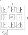
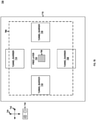
FIG. 3B shows a conceptual illustration of a top-view of thethird MTJ element 300 ofFIG. 3A . In the example ofFIGS. 3A and3B ,third MTJ element 300 includestunnel barriers tunnel barrier 108 ofFIG. 1 . Although not shown, each one oftunnel barriers tunnel barriers tunnel barriers free layer 304 to detect asquare motion 360. In some examples,tunnel barriers free layer 304 to detect rectangular motion. -
FIG. 4A shows a conceptual illustration of a cross-sectional view of afourth MTJ element 400 configured to detect gyroscopic motion.MTJ element 400 may includesupport structure 402,free layer 404,magnetized portion 406,tunnel barrier 408, pinnedlayer 410,bottom electrode 412,base layer 414,substrate 416,metal 418, and via 420, which may be examples ofsupport structure 102,free layer 104,magnetized portion 106,tunnel barrier 108, pinnedlayer 110,bottom electrode 112,base layer 114,substrate 116,metal 118, and via 120 ofFIG. 1 , respectively. In the example ofFIG. 4A ,free layer 404 is spaced next totunnel barrier 408 alongvertical direction 440. In some examples,magnetized portion 406 is spaced next totunnel barrier 408 alongvertical direction 440. For instance, as shown,magnetized portion 406 may be arranged above pinnedlayer 410 and coplanar withtunnel barrier 408. As shown,free layer 404 and/ormagnetized portion 406 may be arranged above pinnedlayer 410 alongvertical direction 440. -
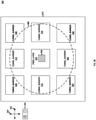
FIG. 4B shows a conceptual illustration of a top-view of thefourth MTJ element 400 ofFIG. 4A . In the example ofFIGS. 4A and4B ,MTJ element 400 includestunnel barriers tunnel barrier 108 ofFIG. 1 . Although not shown, each one oftunnel barriers tunnel barriers tunnel barriers free layer 404 to detect a circular motion 460. In some examples,tunnel barriers free layer 404 to detect ovoid motion. In some examples,tunnel barriers free layer 404 to detect quasi-circular motion. - In the example of
FIGS. 4A and4B ,tunnel barrier 430 is arranged right offree layer 404 along firsthorizontal direction 442. In this example,tunnel barrier 432 is arranged left offree layer 404 along firsthorizontal direction 442. In this example,tunnel barrier 408 is arranged belowfree layer 404 along secondhorizontal direction 444. In this example,tunnel barrier 434 is arranged abovefree layer 404 along secondhorizontal direction 444. Further, as shown,tunnel barrier 435 is arranged left offree layer 404 along firsthorizontal direction 442 and abovefree layer 404 along secondhorizontal direction 444.Tunnel barrier 436 may be arranged right offree layer 404 along firsthorizontal direction 442 and abovefree layer 404 along secondhorizontal direction 444.Tunnel barrier 437 is arranged left offree layer 404 along firsthorizontal direction 442 and belowfree layer 404 along secondhorizontal direction 444.Tunnel barrier 438 is arranged right offree layer 404 along firsthorizontal direction 442 and belowfree layer 404 along secondhorizontal direction 444. -
FIG. 5A shows a conceptual illustration of a cross-sectional view of afifth MTJ element 500 configured to detect gyroscopic motion.MTJ element 500 may includesupport structure 502,free layer 504,magnetized portion 506,tunnel barrier 508, pinnedlayer 510,bottom electrode 512,base layer 514,substrate 516,metal 518, and via 520, which may be examples ofsupport structure 102,free layer 104,magnetized portion 106,tunnel barrier 108, pinnedlayer 110,bottom electrode 112,base layer 114,substrate 116,metal 118, and via 120 ofFIG. 1 , respectively. In the example ofFIG. 5A ,support structure 502 is arranged left oftunnel barrier 508 along firsthorizontal direction 542. -
FIG. 5B shows a conceptual illustration of a top-view of thefifth MTJ element 500 ofFIG. 5A . In the example ofFIGS. 5A and5B ,fifth MTJ element 500 includestunnel barriers tunnel barrier 508. Although not shown, each one oftunnel barriers tunnel barriers tunnel barriers free layer 504 to detect asquare motion 560. In some examples,tunnel barriers free layer 504 to detect a rectangular motion. - As shown,
tunnel barrier 530 is arranged right offree layer 504 along firsthorizontal direction 542. In this example,tunnel barrier 532 is arranged left offree layer 504 along firsthorizontal direction 542. In this example,tunnel barrier 508 is arranged belowfree layer 504 along secondhorizontal direction 544. In this example,tunnel barrier 534 is arranged abovefree layer 504 along secondhorizontal direction 544. -
FIG. 6A shows a conceptual illustration of a cross-sectional view of asixth MTJ element 600 configured to detect gyroscopic motion.MTJ element 600 may includesupport structure 602,free layer 604,magnetized portion 606,tunnel barrier 608, pinnedlayer 610,bottom electrode 612,base layer 614,substrate 616, metal 618, and via 620, which may be examples ofsupport structure 102,free layer 104,magnetized portion 106,tunnel barrier 108, pinnedlayer 110,bottom electrode 112,base layer 114,substrate 116,metal 118, and via 120 ofFIG. 1 , respectively. In the example ofFIG. 6A ,support structure 602 is arranged left oftunnel barrier 608 along firsthorizontal direction 642. -
FIG. 6B shows a conceptual illustration of a top-view of thesixth MTJ element 600 ofFIG. 6A . In the example ofFIGS. 6A and6B ,MTJ element 600 includestunnel barriers tunnel barrier 108 ofFIG. 1 . Although not shown, each one oftunnel barriers tunnel barriers tunnel barriers free layer 604 to detect a circular motion 660. In some examples,tunnel barriers free layer 604 to detect ovoid motion. In some examples,tunnel barriers free layer 604 to detect quasi-circular motion. - In the example of
FIGS. 6A and6B ,tunnel barrier 630 is arranged right offree layer 604 along firsthorizontal direction 642. In this example,tunnel barrier 632 is arranged left offree layer 604 along firsthorizontal direction 642. In this example,tunnel barrier 608 is arranged belowfree layer 604 along secondhorizontal direction 644. In this example,tunnel barrier 634 is arranged abovefree layer 604 along secondhorizontal direction 644. Further, as shown,tunnel barrier 635 is arranged left offree layer 604 along firsthorizontal direction 642 and abovefree layer 604 along secondhorizontal direction 644.Tunnel barrier 636 may be arranged right offree layer 604 along firsthorizontal direction 642 and abovefree layer 604 along secondhorizontal direction 644.Tunnel barrier 637 is arranged left offree layer 604 along firsthorizontal direction 642 and belowfree layer 604 along secondhorizontal direction 644.Tunnel barrier 638 is arranged right offree layer 604 along firsthorizontal direction 642 and belowfree layer 604 along secondhorizontal direction 644. -
FIG. 7A shows a conceptual illustration of a cross-sectional view of aseventh MTJ element 700 configured to detect gyroscopic motion.MTJ element 700 may includesupport structure 702,free layer 704,magnetized portion 706,tunnel barrier 708, pinnedlayer 710,bottom electrode 712,base layer 714,substrate 716,metal 718, and via 720, which may be examples ofsupport structure 102,free layer 104,magnetized portion 106,tunnel barrier 108, pinnedlayer 110,bottom electrode 112,base layer 114,substrate 116,metal 118, and via 120 ofFIG. 1 , respectively. In the example ofFIG. 7A ,free layer 704 is spaced next totunnel barrier 708 alongvertical direction 740. In some examples,magnetized portion 706 is spaced next totunnel barrier 708 alongvertical direction 740. For instance, as shown,magnetized portion 706 may be arranged above pinnedlayer 710 and coplanar withtunnel barrier 708. In the example ofFIG. 7A ,support structure 702 is arranged left oftunnel barrier 708 along firsthorizontal direction 742. -
FIG. 7B shows a conceptual illustration of a top-view of theseventh MTJ element 700 ofFIG. 7A . In the example ofFIGS. 7A and7B ,seventh MTJ element 700 includestunnel barriers tunnel barrier 708. Although not shown, each one oftunnel barriers tunnel barriers tunnel barriers free layer 704 to detect asquare motion 760. In some examples,tunnel barriers free layer 704 to detect a rectangular motion. - As shown,
tunnel barrier 730 is arranged right offree layer 704 along firsthorizontal direction 742. In this example,tunnel barrier 732 is arranged left offree layer 704 along firsthorizontal direction 742. In this example,tunnel barrier 708 is arranged belowfree layer 704 along secondhorizontal direction 744. In this example,tunnel barrier 734 is arranged abovefree layer 704 along secondhorizontal direction 744. -
FIG. 8A shows a conceptual illustration of a cross-sectional view of aneighth MTJ element 800 configured to detect gyroscopic motion.MTJ element 800 may includesupport structure 802,free layer 804,magnetized portion 806,tunnel barrier 808, pinnedlayer 810,bottom electrode 812,base layer 814,substrate 816,metal 818, and via 820, which may be examples ofsupport structure 102,free layer 104,magnetized portion 106,tunnel barrier 108, pinnedlayer 110,bottom electrode 112,base layer 114,substrate 116,metal 118, and via 120 ofFIG. 1 , respectively. In the example ofFIG. 8A ,free layer 804 is spaced next totunnel barrier 808 alongvertical direction 840. For instance, as shown,magnetized portion 806 may be arranged above pinnedlayer 810 and coplanar withtunnel barrier 808. In some examples,magnetized portion 806 is spaced next totunnel barrier 808 alongvertical direction 840. In the example ofFIG. 8A ,support structure 802 is arranged left oftunnel barrier 808 along firsthorizontal direction 842. -
FIG. 8B shows a conceptual illustration of a top-view of theeighth MTJ element 800 ofFIG. 8A . In the example ofFIGS. 8A and8B ,eighth MTJ element 800 includestunnel barriers tunnel barrier 108 ofFIG. 1 . Although not shown, each one oftunnel barriers tunnel barriers tunnel barriers free layer 804 to detect acircular motion 860. In some examples,tunnel barriers free layer 804 to detect ovoid motion. In some examples,tunnel barriers free layer 804 to detect quasi-circular motion. - In the example of
FIGS. 8A and8B ,tunnel barrier 830 is arranged right offree layer 804 along firsthorizontal direction 842. In this example,tunnel barrier 832 is arranged left offree layer 804 along firsthorizontal direction 842. In this example,tunnel barrier 808 is arranged belowfree layer 804 along secondhorizontal direction 844. In this example,tunnel barrier 834 is arranged abovefree layer 804 along secondhorizontal direction 844. Further, as shown,tunnel barrier 835 is arranged left offree layer 804 along firsthorizontal direction 842 and abovefree layer 804 along secondhorizontal direction 844.Tunnel barrier 836 may be arranged right offree layer 804 along firsthorizontal direction 842 and abovefree layer 804 along secondhorizontal direction 844.Tunnel barrier 837 is arranged left offree layer 804 along firsthorizontal direction 842 and belowfree layer 804 along secondhorizontal direction 844.Tunnel barrier 838 is arranged right offree layer 804 along firsthorizontal direction 842 and belowfree layer 804 along secondhorizontal direction 844. -
FIG. 9A shows a conceptual illustration of a cross-sectional view of aninth MTJ element 900 configured to detect gyroscopic motion.MTJ element 900 may includefree layer 904,magnetized portion 906,tunnel barrier 908, pinned layer 910, bottom electrode 912,base layer 914, andsubstrate 916, which may be examples offree layer 104,magnetized portion 106,tunnel barrier 108, pinnedlayer 110,bottom electrode 112,base layer 114, andsubstrate 116 ofFIG. 1 , respectively. - In the example of
FIG. 9A ,free layer 904 extends frombase layer 914 alongvertical direction 940. As shown, pinned layer 910 is arranged abovebase layer 914 andfree layer 904 extends alongvertical direction 940 away frombase layer 914. In this example,free layer 904 includesmagnetized portion 906 arranged above pinned layer 910 and coplanar withtunnel barrier 908. -
FIG. 9B shows a conceptual illustration of a top-view of theninth MTJ element 900 ofFIG. 9A . In the example ofFIGS. 9A and9B ,MTJ element 900 includestunnel barriers tunnel barrier 908. Although not shown, each one oftunnel barriers tunnel barriers tunnel barriers free layer 904 to detect asquare motion 960. In some examples,tunnel barriers free layer 904 to detect a rectangular motion. - As shown,
tunnel barrier 930 is arranged right offree layer 904 along firsthorizontal direction 942. In this example,tunnel barrier 932 is arranged left offree layer 904 along firsthorizontal direction 942. In this example,tunnel barrier 908 is arranged belowfree layer 904 along secondhorizontal direction 944. In this example,tunnel barrier 934 is arranged abovefree layer 904 along secondhorizontal direction 944. -
FIG. 10A shows a conceptual illustration of a cross-sectional view of atenth MTJ element 1000 configured to detect gyroscopic motion.MTJ element 1000 may includefree layer 1004, magnetizedportion 1006,tunnel barrier 1008, pinned layer 1010,bottom electrode 1012,base layer 1014, andsubstrate 1016, which may be examples offree layer 104,magnetized portion 106,tunnel barrier 108, pinnedlayer 110,bottom electrode 112,base layer 114, andsubstrate 116 ofFIG. 1 , respectively. - In the example of
FIG. 10A ,free layer 1004 extends frombase layer 1014 alongvertical direction 1040. As shown, pinned layer 1010 is arranged abovebase layer 1014 andfree layer 1004 extends alongvertical direction 1040 away frombase layer 1014. In this example,free layer 1004 includes magnetizedportion 1006 arranged above pinned layer 1010 and coplanar withtunnel barrier 1008. -
FIG. 10B shows a conceptual illustration of a top-view of thetenth MTJ element 1000 ofFIG. 10A . In the example ofFIGS. 10A and10B ,MTJ element 1000 includestunnel barriers tunnel barrier 108 ofFIG. 1 . Although not shown, each one oftunnel barriers tunnel barriers tunnel barriers free layer 1004 to detect a circular motion 1060. In some examples,tunnel barriers free layer 1004 to detect ovoid motion. In some examples,tunnel barriers free layer 1004 to detect quasi-circular motion. - In the example of
FIGS. 10A and10B ,tunnel barrier 1030 is arranged right offree layer 1004 along firsthorizontal direction 1042. In this example,tunnel barrier 1032 is arranged left offree layer 1004 along firsthorizontal direction 1042. In this example,tunnel barrier 1008 is arranged belowfree layer 1004 along secondhorizontal direction 1044. In this example,tunnel barrier 1034 is arranged abovefree layer 1004 along secondhorizontal direction 1044. Further, as shown,tunnel barrier 1035 is arranged left offree layer 1004 along firsthorizontal direction 1042 and abovefree layer 1004 along secondhorizontal direction 1044.Tunnel barrier 1036 may be arranged right offree layer 1004 along firsthorizontal direction 1042 and abovefree layer 1004 along secondhorizontal direction 1044.Tunnel barrier 1037 is arranged left offree layer 1004 along firsthorizontal direction 1042 and belowfree layer 1004 along secondhorizontal direction 1044.Tunnel barrier 1038 is arranged right offree layer 1004 along firsthorizontal direction 1042 and belowfree layer 1004 along secondhorizontal direction 1044. -
FIG. 11 shows a conceptual illustration of a firstgyroscopic sensor device 1100 that may be used to implement the techniques of the present disclosure.Gyroscopic sensor device 1100 may includesupport structure 1102,bottom electrode 1112,base layer 1114,processing circuity 1116,metal 1118, and via 1120, which may be examples ofsupport structure 102,bottom electrode 112,base layer 114,substrate 116,metal 118, and via 120 ofFIG. 1 , respectively.Gyroscopic sensor device 1100 may further includesensor module 1103, which may comprise a free layer, one or more tunnel barriers, and one or more pinned layers arranged for detecting gyroscopic motion using a support structure (e.g., seeFIGS. 1A-1D ,2A-2B ,3A-3B ,4A-4B .5A-5B ,6A-6B ,7A-7B , and8A-8B ). For example, whileFIG. 11 illustrates a single bottom electrode, some examples, may include two or more (e.g., 4, 8, etc.) bottom electrodes that are each connected to a respective pinned layer and a respective tunnel barrier. - Sensor devices implementing one or more of the techniques described in this disclosure may be implemented in a wide array of electronic devices ranging from small portable devices such as music players, smart phones, game cartridges, and memory sticks up to larger devices such as tablet computers, gaming devices or consoles, desktop computers, super computers, and enterprise storage solutions.
-
Support structure 1102 may include via 1150 adapted to electrically couple a free layer ofsensor module 1103 toprocessing circuitry 1116. Via 1150 and via 1152 may be formed of an electrically conductive material, such as, for example, but not limited to, tungsten, aluminum, aluminum-copper, and/or copper. In the example ofFIG. 11 , via 1150 electrically connectsmetal 1118 toprocessing circuity 1116. In this example, via 1152 electrically connectsbottom electrode 1112 toprocessing circuity 1116. -
Processing circuitry 1116 is configured to monitor the resistance(s) and/or magnetoresistance(s) ofsensor module 1103, which may correspond to gyroscopic motion ofgyroscopic sensor device 1100. This monitoring of the resistance(s) and/or magnetoresistance(s) is termed Rmonitor, which represents the real time measuring of the MTJ element resistance(s) and/or magnetoresistance(s). For example,processing circuitry 1116 may determine an angular velocity is increasing as a magnitude of resistance and/or magnetoresistance between a free layer and a particular pinned layer ofsensor module 1103 decreases. -
Processing circuitry 1116 may be adapted to compare two or more respective resistances between each pinned layer and the free layer to determine gyroscopic motion. For example,processing circuitry 1116 may compare a first resistance between a respective pinned layer fortunnel barrier 130 andfree layer 104 to a second resistance between a respective pinned layer fortunnel barrier 132 andfree layer 104 to determine gyroscopic motion along firsthorizontal direction 142. In some examples,processing circuitry 1116 may compare a third resistance between a respective pinned layer fortunnel barrier 108 andfree layer 104 to a fourth resistance between a respective pinned layer fortunnel barrier 134 andfree layer 104 to determine gyroscopic motion along secondhorizontal direction 144. -
Processing circuitry 1116 may be adapted to determine gyroscopic motion has occurred along firsthorizontal direction 142. For example,processing circuitry 1116 may determine gyroscopic motion has occurred along firsthorizontal direction 142 when a first resistance between a respective pinned layer fortunnel barrier 130 andfree layer 104 is greater than a second resistance between a respective pinned layer fortunnel barrier 132 andfree layer 104. Similarly,processing circuitry 1116 may determine gyroscopic motion has occurred along firsthorizontal direction 142 when a first resistance between a respective pinned layer fortunnel barrier 130 andfree layer 104 is less than a second resistance between a respective pinned layer fortunnel barrier 132 andfree layer 104. -
Processing circuitry 1116 may be adapted to determine gyroscopic motion has occurred along secondhorizontal direction 144. For example,processing circuitry 1116 may determine gyroscopic motion has occurred along secondhorizontal direction 144 when a third resistance between a respective pinned layer fortunnel barrier 108 andfree layer 104 is greater than a fourth resistance between a respective pinned layer fortunnel barrier 134 andfree layer 104 to determine gyroscopic motion along secondhorizontal direction 144. Similarly,processing circuitry 1116 may determine gyroscopic motion has occurred along secondhorizontal direction 144 when a third resistance between a respective pinned layer fortunnel barrier 108 andfree layer 104 is less than a fourth resistance between a respective pinned layer fortunnel barrier 134 andfree layer 104 to determine gyroscopic motion along secondhorizontal direction 144. -
Processing circuitry 1116 may be adapted to output an indication of the gyroscopic motion. For example,processing circuitry 1116 may generate a digital signal indicating gyroscopic motion along firsthorizonal direction 142 and/or secondhorizonal direction 144. In some examples,processing circuitry 1116 may generate one or more voltages magnitudes indicating gyroscopic motion along firsthorizonal direction 142 and/or secondhorizonal direction 144. -
Processing circuitry 1116 may include one or more processors, including one or more microprocessors, digital signal processors (DSPs), ASICs, field programmable gate arrays (FPGAs), or any other equivalent integrated or discrete logic circuitry, as well as any combinations of such components. The term "processor" or "processing circuitry" may generally refer to any of the foregoing logic circuitry, alone or in combination with other logic circuitry, or any other equivalent circuitry. Although the foregoing examples are directed toMTJ element 100 ofFIGS. 1A-1D , other examples may use other MTJ elements (e.g., 2A-2B, 3A-3B, 4A-4B. 5A-5B, 6A-6B, 7A-7B, 8A-8B, etc.) -
FIG. 12 shows a conceptual illustration of a secondgyroscopic sensor device 1200 that may be used to implement the techniques of the present disclosure.Gyroscopic sensor device 1200 may includebottom electrode 1212,base layer 1214, andprocessing circuity 1216, which may be examples ofbottom electrode 112,base layer 114, andsubstrate 116 ofFIG. 1 , respectively.Gyroscopic sensor device 1200 may further includesensor module 1203, which may comprise a free layer, one or more tunnel barriers, and one or more pinned layers arranged for detecting gyroscopic motion (e.g., seeFIGS. 9A-9B , and10A-10B ). For example, whileFIG. 12 illustrates a single bottom electrode, some examples, may include two or more (e.g., 4, 8, etc.) bottom electrodes that are each connected to a respective pinned layer and a respective tunnel barrier. - Sensor devices implementing one or more of the techniques described in this disclosure may be implemented in a wide array of electronic devices ranging from small portable devices such as music players, smart phones, game cartridges, and memory sticks up to larger devices such as tablet computers, gaming devices or consoles, desktop computers, super computers, and enterprise storage solutions.
- In the example of
FIG. 12 ,base layer 1214 comprises via 1250 adapted to electrically couple a free layer ofsensor module 1203 toprocessing circuitry 1216. Via 1250 and via 1252 may be formed of an electrically conductive material, such as, for example, but not limited to, copper. In the example ofFIG. 12 , via 1250 electrically connects a free layer ofsensor module 1203 toprocessing circuity 1216. In this example, via 1252 electrically connectsbottom electrode 1212 toprocessing circuity 1216. -
Processing circuitry 1216 is configured to monitor the resistance(s) and/or magnetoresistance(s) ofsensor module 1203, which may correspond to gyroscopic motion ofgyroscopic sensor device 1200. This monitoring of the resistance(s) and/or magnetoresistance(s) is termed Rmonitor, which represents the real time measuring of the MTJ element resistance(s) and/or magnetoresistance(s). For example,processing circuitry 1216 may determine an angular velocity is increasing as a magnitude of resistance and/or magnetoresistance between a free layer and a particular tunnel barrier ofsensor module 1203 decreases. -
Processing circuitry 1216 may be adapted to compare two or more respective resistances between each pinned layer and the free layer to determine gyroscopic motion. For example,processing circuitry 1216 may compare a first resistance between a respective pinned layer fortunnel barrier 930 andfree layer 904 to a second resistance between a respective pinned layer fortunnel barrier 932 andfree layer 904 to determine gyroscopic motion along firsthorizontal direction 942. In some examples,processing circuitry 1216 may compare a third resistance between a respective pinned layer fortunnel barrier 908 andfree layer 904 to a fourth resistance between a respective pinned layer fortunnel barrier 934 andfree layer 904 to determine gyroscopic motion along secondhorizontal direction 944. -
Processing circuitry 1216 may be adapted to determine gyroscopic motion has occurred along firsthorizontal direction 942. For example,processing circuitry 1216 may determine gyroscopic motion has occurred along firsthorizontal direction 942 when a first resistance between a respective pinned layer fortunnel barrier 930 andfree layer 904 is greater than a second resistance between a respective pinned layer fortunnel barrier 932 andfree layer 904. Similarly,processing circuitry 1216 may determine gyroscopic motion has occurred along firsthorizontal direction 942 when a first resistance between a respective pinned layer fortunnel barrier 930 andfree layer 904 is less than a second resistance between a respective pinned layer fortunnel barrier 932 andfree layer 904. -
Processing circuitry 1216 may be adapted to determine gyroscopic motion has occurred along secondhorizontal direction 944. For example,processing circuitry 1216 may determine gyroscopic motion has occurred along secondhorizontal direction 944 when a third resistance between a respective pinned layer fortunnel barrier 908 andfree layer 904 is greater than a fourth resistance between a respective pinned layer fortunnel barrier 934 andfree layer 904 to determine gyroscopic motion along secondhorizontal direction 944. Similarly,processing circuitry 1216 may determine gyroscopic motion has occurred along secondhorizontal direction 944 when a third resistance between a respective pinned layer fortunnel barrier 908 andfree layer 904 is less than a fourth resistance between a respective pinned layer fortunnel barrier 934 andfree layer 904 to determine gyroscopic motion along secondhorizontal direction 944. -
Processing circuitry 1216 may be adapted to output an indication of the gyroscopic motion. For example,processing circuitry 1216 may generate a digital signal indicating gyroscopic motion along firsthorizonal direction 942 and/or secondhorizonal direction 944. In some examples,processing circuitry 1216 may generate one or more voltages magnitudes indicating gyroscopic motion along firsthorizonal direction 942 and/or secondhorizonal direction 944. -
Processing circuitry 1216 may include one or more processors, including one or more microprocessors, digital signal processors (DSPs), ASICs, field programmable gate arrays (FPGAs), or any other equivalent integrated or discrete logic circuitry, as well as any combinations of such components. Although the foregoing examples are directed toMTJ element 100 ofFIGS. 1A-1D , other examples may use other MTJ elements (e.g., 2A-2B, 3A-3B, 4A-4B. 5A-5B, 6A-6B, 7A-7B, 8A-8B, etc.) -
FIG. 13 shows a flowchart of operations for detecting gyroscopic motion in accordance with the techniques of this disclosure. The operations ofFIG. 13 may, for example, be performed by a MTJ element described above with respect to any combination ofFIGS. 1A-1D ,2A-2B ,3A-3B ,4A-4B .5A-5B ,6A-6B ,7A-7B ,8A-8B ,9A-9B ,10A-10B ,11 , and12 .Processing circuitry 1116 and/orprocessing circuitry 1216 measures a resistance at a MTJ element (1302).Processing circuitry 1116 and/orprocessing circuitry 1216 determines gyroscopic motion based on the resistance at the MTJ element (1304). For instance,processing circuitry 1116 and/orprocessing circuitry 1216 determines gyroscopic motion based on a resistance atsensor module 1103 and/orsensor module 1203.Processing circuitry 1116 and/orprocessing circuitry 1216 outputs an indication of the gyroscopic motion (1306). - The term "circuitry" as used herein may refer to any of the foregoing structure or any other structure suitable for processing program code and/or data or otherwise implementing the techniques described herein. Circuitry may, for example, any of a variety of types of solid state circuit elements, such as CPUs, CPU cores, GPUs, DSPs, ASICs, mixed-signal integrated circuits, FPGAs, microcontrollers, programmable logic controllers (PLCs), programmable logic device (PLDs), complex PLDs (CPLDs), systems on a chip (SoC), any subsection of any of the above, an interconnected or distributed combination of any of the above, or any other integrated or discrete logic circuitry, or any other type of component or one or more components capable of being configured in accordance with any of the examples disclosed herein.
- As used in this disclosure, circuitry may also include one or more memory devices, such as any volatile or non-volatile media, such as a RAM, ROM, non-volatile RAM (NVRAM), electrically erasable programmable ROM (EEPROM), flash memory, and the like. The one or more memory devices may store computer-readable instructions that, when executed or processed the circuitry, cause the circuitry to implement the techniques attributed herein to circuitry. The circuitry of this disclosure may be programmed, or otherwise controlled, with various forms of firmware and/or software.
- Various illustrative aspects of the disclosure have been described above. These and other aspects are within the scope of the following claims.
Claims (16)
- A magnetic tunnel junction (MTJ) based sensor device (1100), the device comprising:a MTJ element (100) comprising a free layer (104), an anti-ferromagnetic pinned layer (110), a tunnel barrier (108), the tunnel barrier being arranged above the pinned layer, wherein the free layer is adapted to flex towards and away from the anti-ferromagnetic pinned layer during gyroscopic motion, wherein a magnetization direction of the anti-ferromagnetic pinned layer remains relatively fixed when operational magnetic fields are applied to MTJ element; andprocessing circuitry (1116) configured to:measure a resistance at the MTJ element; anddetermine gyroscopic motion based on the resistance at the MTJ element.
- The device of claim 1, wherein the free layer includes a magnetization direction that is free to switch between a parallel orientation and an anti-parallel orientation.
- The device of claim 1, wherein the MTJ element comprises a support structure (102) adapted to arrange the free layer above the tunnel barrier.
- The device of claim 3, wherein the free layer comprises a magnetized portion (106) arranged above the tunnel barrier.
- The device of claim 3, wherein the free layer comprises a magnetized portion (106) arranged above the pinned layer and coplanar with the tunnel barrier.
- The device of claim 3, wherein the support structure comprises a via (120) adapted to electrically couple the free layer to processing circuitry.
- The device of claim 1, wherein the MTJ element comprises:
a base layer (114), wherein the pinned layer is arranged above the base layer, and wherein the free layer extends along a vertical direction (140) away from the base layer. - The device of claim 7, wherein the free layer comprises a magnetized portion (106) arranged above the pinned layer and coplanar with the tunnel barrier.
- The device of claim 7, wherein the base layer comprises a via (120) adapted to electrically couple the free layer to processing circuitry.
- The device of claim 1, wherein the MTJ element comprises:a plurality of pinned layers (110) that includes the anti-ferromagnetic pinned layer; anda plurality of tunnel barriers (108, 130, 132, 134) that includes the tunnel barrier (108), each tunnel barrier of the plurality of tunnel barriers being arranged above a respective pinned layer of the plurality of pinned layers,wherein, to measure the resistance at the MTJ element, the processing circuitry is adapted to measure a respective resistance between each pinned layer of the plurality of pinned layers and the free layer.
- The device of claim 10, wherein, to determine gyroscopic motion, the processing circuitry is adapted to:
compare two or more of the respective resistances. - The device of claim 10, wherein the anti-ferromagnetic pinned layer is a first pinned layer (110), wherein the plurality of pinned layers comprises a second pinned layer arranged along a first horizontal direction (142) on an opposite side of the free layer from the first pinned layer, and wherein, to determine gyroscopic motion, the processing circuitry is adapted to:
determine gyroscopic motion has occurred along the first horizontal direction when a first resistance between the first pinned layer and the free layer is greater than a second resistance between the second pinned layer and the free layer. - The device of claim 12, wherein the plurality of pinned layers comprises a third pinned layer, wherein the plurality of pinned layers comprises a fourth pinned layer arranged along a second horizontal direction (144) on an opposite side of the free layer from the third pinned layer, wherein the second horizontal direction is perpendicular with the first horizontal direction, and wherein, to determine gyroscopic motion, the processing circuitry is adapted to:
determine gyroscopic motion has occurred along the second horizontal direction when a third resistance between the third pinned layer and the free layer is greater than a fourth resistance between the fourth pinned layer and the free layer. - The device of claim 10, wherein the plurality of pinned layers is arranged relative to the free layer to detect a rectangular motion.
- The device of claim 10, wherein the plurality of pinned layer is arranged relative to the free layer to detect a circular motion (260).
- A method for detecting gyroscopic motion using a magnetic tunnel junction (MTJ) based sensor device (1100), the method comprising:applying operational magnetic fields to a MTJ element (100), wherein the MTJ element comprises a free layer (104), an anti-ferromagnetic pinned layer (110), and a tunnel barrier (108), the tunnel barrier being arranged above the pinned layer and wherein the free layer is adapted to flex towards and/or away from the tunnel barrier during gyroscopic motion;wherein a magnetization direction of the anti-ferromagnetic pinned layer remains relatively fixed when the operational magnetic fields are applied to MTJ element;measuring (1302), by processing circuitry, a resistance at the MTJ elementdetermining (1304), by the processing circuitry, gyroscopic motion based on the resistance at the MTJ element; andoutputting (1306), by the processing circuitry, an indication of the gyroscopic motion.
Applications Claiming Priority (2)
| Application Number | Priority Date | Filing Date | Title |
|---|---|---|---|
| US201862729881P | 2018-09-11 | 2018-09-11 | |
| US16/195,515 US10876839B2 (en) | 2018-09-11 | 2018-11-19 | Spintronic gyroscopic sensor device |
Publications (2)
| Publication Number | Publication Date |
|---|---|
| EP3623757A1 EP3623757A1 (en) | 2020-03-18 |
| EP3623757B1 true EP3623757B1 (en) | 2022-01-26 |
Family
ID=67875270
Family Applications (1)
| Application Number | Title | Priority Date | Filing Date |
|---|---|---|---|
| EP19195761.2A Active EP3623757B1 (en) | 2018-09-11 | 2019-09-05 | Spintronic gyroscopic sensor device |
Country Status (2)
| Country | Link |
|---|---|
| US (1) | US10876839B2 (en) |
| EP (1) | EP3623757B1 (en) |
Families Citing this family (2)
| Publication number | Priority date | Publication date | Assignee | Title |
|---|---|---|---|---|
| US10871529B2 (en) * | 2018-09-11 | 2020-12-22 | Honeywell International Inc. | Spintronic mechanical shock and vibration sensor device |
| US11054438B2 (en) * | 2019-03-29 | 2021-07-06 | Honeywell International Inc. | Magnetic spin hall effect spintronic accelerometer |
Family Cites Families (39)
| Publication number | Priority date | Publication date | Assignee | Title |
|---|---|---|---|---|
| US5756895A (en) | 1995-09-01 | 1998-05-26 | Hughes Aircraft Company | Tunneling-based rate gyros with simple drive and sense axis coupling |
| US5764567A (en) * | 1996-11-27 | 1998-06-09 | International Business Machines Corporation | Magnetic tunnel junction device with nonferromagnetic interface layer for improved magnetic field response |
| US5859368A (en) | 1996-04-15 | 1999-01-12 | Cargille; Donald R. | Tunneling-based rotation rate sensor |
| US5962782A (en) | 1997-06-11 | 1999-10-05 | The Broken Hill Proprietary Company Limited | Gravity gradiometer accelerometers |
| JPH11352143A (en) | 1998-04-06 | 1999-12-24 | Matsushita Electric Ind Co Ltd | Acceleration sensor |
| US6052263A (en) | 1998-08-21 | 2000-04-18 | International Business Machines Corporation | Low moment/high coercivity pinned layer for magnetic tunnel junction sensors |
| US6507187B1 (en) | 1999-08-24 | 2003-01-14 | The United States Of America As Represented By The Administrator Of The National Aeronautics And Space Administration | Ultra-sensitive magnetoresistive displacement sensing device |
| US7145330B2 (en) | 2002-08-16 | 2006-12-05 | Brown University Research Foundation | Scanning magnetic microscope having improved magnetic sensor |
| JP2005302876A (en) | 2004-04-08 | 2005-10-27 | Denso Corp | Tunnel magnetoresistive effect element, manufacturing method and manufacturing apparatus thereof |
| US7547480B2 (en) * | 2005-10-28 | 2009-06-16 | Everspin Technologies, Inc. | Magnetic tunnel junction pressure sensors and methods |
| US7239543B2 (en) | 2005-10-28 | 2007-07-03 | Freescale Semiconductor, Inc. | Magnetic tunnel junction current sensors |
| US7732881B2 (en) | 2006-11-01 | 2010-06-08 | Avalanche Technology, Inc. | Current-confined effect of magnetic nano-current-channel (NCC) for magnetic random access memory (MRAM) |
| EP1863034B1 (en) | 2006-05-04 | 2011-01-05 | Hitachi, Ltd. | Magnetic memory device |
| AT503995B1 (en) | 2006-08-07 | 2009-03-15 | Arc Seibersdorf Res Gmbh | MINIATURE SENSOR ACCELERATION |
| US7690263B2 (en) | 2006-11-24 | 2010-04-06 | Academia Sinica | Strain sensor and a method of making the same |
| TWI333208B (en) * | 2007-03-26 | 2010-11-11 | Ind Tech Res Inst | Magnetic memory and method for manufacturing the same |
| US7635974B2 (en) | 2007-05-02 | 2009-12-22 | Magic Technologies, Inc. | Magnetic tunnel junction (MTJ) based magnetic field angle sensor |
| FR2918761B1 (en) | 2007-07-10 | 2009-11-06 | Commissariat Energie Atomique | MAGNETIC FIELD SENSOR WITH LOW NOISE. |
| JP5360596B2 (en) | 2007-08-03 | 2013-12-04 | 日本電気株式会社 | Magnetic random access memory and manufacturing method thereof |
| US9250070B2 (en) | 2011-11-16 | 2016-02-02 | Keith Robert Wootten | Rugged three-axis inclinometer |
| US8698260B2 (en) * | 2012-02-29 | 2014-04-15 | Headway Technologies, Inc. | Engineered magnetic layer with improved perpendicular anisotropy using glassing agents for spintronic applications |
| US9254992B2 (en) | 2012-07-27 | 2016-02-09 | Tao Ju | Method of making a MEMS gyroscope having a magnetic source and a magnetic sensing mechanism |
| US20140026658A1 (en) | 2012-07-27 | 2014-01-30 | Biao Zhang | Mems device and a method of using the same |
| CN102853826A (en) | 2012-09-07 | 2013-01-02 | 中北大学 | Silicon base tunneling magnetoresistance micro gyroscope |
| US8836056B2 (en) * | 2012-09-26 | 2014-09-16 | Intel Corporation | Perpendicular MTJ stacks with magnetic anisotropy enhancing layer and crystallization barrier layer |
| US8830737B2 (en) * | 2012-12-17 | 2014-09-09 | Avalanche Technology, Inc. | Method and apparatus for sensing the state of a magnetic tunnel junction (MTJ) |
| WO2016007126A1 (en) | 2014-07-07 | 2016-01-14 | Intel Corporation | Spin-transfer torque memory (sttm) devices having magnetic contacts |
| EP2966453B1 (en) | 2014-07-11 | 2018-10-31 | Crocus Technology | MLU based accelerometer using a magnetic tunnel junction |
| KR102419536B1 (en) | 2014-07-17 | 2022-07-11 | 코넬 유니버시티 | Circuits and devices based on enhanced spin hall effect for efficient spin transfer torque |
| CN104567848B (en) | 2015-01-28 | 2017-09-29 | 中北大学 | A kind of micromechanical gyro based on tunnel magneto-resistance effect |
| CN105180914B (en) | 2015-10-21 | 2017-11-17 | 中北大学 | A kind of micromechanical gyro of the high q-factor tunnel magneto-resistance effect detected in face |
| US9489998B1 (en) * | 2015-11-17 | 2016-11-08 | Samsung Electronics Co., Ltd. | Magnetic junctions having a magnetoelastic free layer programmable using spin transfer torque |
| US10592802B2 (en) | 2016-02-28 | 2020-03-17 | Purdue Research Foundation | Electronic synapse having spin-orbit torque induced spike-timing dependent plasticity |
| CN206132803U (en) | 2016-10-26 | 2017-04-26 | 东南大学 | Tunnel magnetoresistive effect accelerometer device based on clearance changes |
| CN106645797B (en) | 2016-10-26 | 2023-09-12 | 东南大学 | A tunnel magnetoresistive effect accelerometer device based on gap change |
| WO2018125142A1 (en) | 2016-12-29 | 2018-07-05 | Intel Corporation | Protection layers for magnetic tunnel junctions |
| KR101825318B1 (en) | 2017-01-03 | 2018-02-05 | 고려대학교 산학협력단 | Magnetic Tunnel Junction Device With Spin-Filter Structure |
| CN107255737B (en) | 2017-05-18 | 2019-12-10 | 东南大学 | Device and method for tunnel magneto-resistive accelerometer based on changing direction of magnetic field |
| CN107421525A (en) | 2017-08-15 | 2017-12-01 | 中北大学 | A kind of tunnel magnetoresistive disresonance type 3 axis MEMS gyro |
-
2018
- 2018-11-19 US US16/195,515 patent/US10876839B2/en active Active
-
2019
- 2019-09-05 EP EP19195761.2A patent/EP3623757B1/en active Active
Non-Patent Citations (1)
| Title |
|---|
| None * |
Also Published As
| Publication number | Publication date |
|---|---|
| US10876839B2 (en) | 2020-12-29 |
| EP3623757A1 (en) | 2020-03-18 |
| US20200080844A1 (en) | 2020-03-12 |
Similar Documents
| Publication | Publication Date | Title |
|---|---|---|
| EP3623820B1 (en) | Spintronic accelerometer | |
| US9255975B2 (en) | Magnetic-field sensing method | |
| US9810748B2 (en) | Tunneling magneto-resistor device for sensing a magnetic field | |
| CN202083786U (en) | Film magnetoresistance sensing element, combination of a plurality of sensing elements, and electronic device coupled with combination | |
| TWI513993B (en) | 3-axis magnetic field sensor, fabrication method of magnetic sensing structure and magnetic field sensing circuit | |
| TW202117355A (en) | Magnetoresistance element, magnetoresistance structure and three-dimensional magnetic field sensor | |
| US20230251331A1 (en) | Sensor unit | |
| Cai et al. | Magnetometer basics for mobile phone applications | |
| EP3623757B1 (en) | Spintronic gyroscopic sensor device | |
| US11054438B2 (en) | Magnetic spin hall effect spintronic accelerometer | |
| EP3623777B1 (en) | Spintronic mechanical shock and vibration sensor device | |
| US11150312B2 (en) | Accelerometer using magnetic tunnel junction | |
| US11791083B2 (en) | Tunnel magneto-resistive (TMR) sensor with perpendicular magnetic tunneling junction (p-MTJ) structures | |
| US11719773B2 (en) | Magnetic field sensor with MTJ elements arranged in series | |
| CN105579860B (en) | Specific integrated circuit with integrated magnetic sensor | |
| CN104868051A (en) | High-sensitivity magnetic sensing device and preparation method thereof | |
| KR20230140079A (en) | Spin-orbit-torque based magnetic sensor and magnetic field measurement method usig the magnetic sensor | |
| CN104880678A (en) | Magnetic sensing device and preparation process thereof |
Legal Events
| Date | Code | Title | Description |
|---|---|---|---|
| PUAI | Public reference made under article 153(3) epc to a published international application that has entered the european phase |
Free format text: ORIGINAL CODE: 0009012 |
|
| STAA | Information on the status of an ep patent application or granted ep patent |
Free format text: STATUS: THE APPLICATION HAS BEEN PUBLISHED |
|
| AK | Designated contracting states |
Kind code of ref document: A1 Designated state(s): AL AT BE BG CH CY CZ DE DK EE ES FI FR GB GR HR HU IE IS IT LI LT LU LV MC MK MT NL NO PL PT RO RS SE SI SK SM TR |
|
| AX | Request for extension of the european patent |
Extension state: BA ME |
|
| STAA | Information on the status of an ep patent application or granted ep patent |
Free format text: STATUS: REQUEST FOR EXAMINATION WAS MADE |
|
| 17P | Request for examination filed |
Effective date: 20200627 |
|
| RBV | Designated contracting states (corrected) |
Designated state(s): AL AT BE BG CH CY CZ DE DK EE ES FI FR GB GR HR HU IE IS IT LI LT LU LV MC MK MT NL NO PL PT RO RS SE SI SK SM TR |
|
| STAA | Information on the status of an ep patent application or granted ep patent |
Free format text: STATUS: EXAMINATION IS IN PROGRESS |
|
| 17Q | First examination report despatched |
Effective date: 20201030 |
|
| GRAP | Despatch of communication of intention to grant a patent |
Free format text: ORIGINAL CODE: EPIDOSNIGR1 |
|
| STAA | Information on the status of an ep patent application or granted ep patent |
Free format text: STATUS: GRANT OF PATENT IS INTENDED |
|
| INTG | Intention to grant announced |
Effective date: 20210528 |
|
| GRAJ | Information related to disapproval of communication of intention to grant by the applicant or resumption of examination proceedings by the epo deleted |
Free format text: ORIGINAL CODE: EPIDOSDIGR1 |
|
| STAA | Information on the status of an ep patent application or granted ep patent |
Free format text: STATUS: EXAMINATION IS IN PROGRESS |
|
| INTC | Intention to grant announced (deleted) | ||
| GRAP | Despatch of communication of intention to grant a patent |
Free format text: ORIGINAL CODE: EPIDOSNIGR1 |
|
| STAA | Information on the status of an ep patent application or granted ep patent |
Free format text: STATUS: GRANT OF PATENT IS INTENDED |
|
| INTG | Intention to grant announced |
Effective date: 20210917 |
|
| GRAS | Grant fee paid |
Free format text: ORIGINAL CODE: EPIDOSNIGR3 |
|
| GRAA | (expected) grant |
Free format text: ORIGINAL CODE: 0009210 |
|
| STAA | Information on the status of an ep patent application or granted ep patent |
Free format text: STATUS: THE PATENT HAS BEEN GRANTED |
|
| AK | Designated contracting states |
Kind code of ref document: B1 Designated state(s): AL AT BE BG CH CY CZ DE DK EE ES FI FR GB GR HR HU IE IS IT LI LT LU LV MC MK MT NL NO PL PT RO RS SE SI SK SM TR |
|
| REG | Reference to a national code |
Ref country code: GB Ref legal event code: FG4D |
|
| REG | Reference to a national code |
Ref country code: CH Ref legal event code: EP |
|
| REG | Reference to a national code |
Ref country code: AT Ref legal event code: REF Ref document number: 1465611 Country of ref document: AT Kind code of ref document: T Effective date: 20220215 |
|
| REG | Reference to a national code |
Ref country code: IE Ref legal event code: FG4D |
|
| REG | Reference to a national code |
Ref country code: DE Ref legal event code: R096 Ref document number: 602019011180 Country of ref document: DE |
|
| REG | Reference to a national code |
Ref country code: LT Ref legal event code: MG9D |
|
| REG | Reference to a national code |
Ref country code: NL Ref legal event code: MP Effective date: 20220126 |
|
| REG | Reference to a national code |
Ref country code: AT Ref legal event code: MK05 Ref document number: 1465611 Country of ref document: AT Kind code of ref document: T Effective date: 20220126 |
|
| PG25 | Lapsed in a contracting state [announced via postgrant information from national office to epo] |
Ref country code: NL Free format text: LAPSE BECAUSE OF FAILURE TO SUBMIT A TRANSLATION OF THE DESCRIPTION OR TO PAY THE FEE WITHIN THE PRESCRIBED TIME-LIMIT Effective date: 20220126 |
|
| PG25 | Lapsed in a contracting state [announced via postgrant information from national office to epo] |
Ref country code: SE Free format text: LAPSE BECAUSE OF FAILURE TO SUBMIT A TRANSLATION OF THE DESCRIPTION OR TO PAY THE FEE WITHIN THE PRESCRIBED TIME-LIMIT Effective date: 20220126 Ref country code: RS Free format text: LAPSE BECAUSE OF FAILURE TO SUBMIT A TRANSLATION OF THE DESCRIPTION OR TO PAY THE FEE WITHIN THE PRESCRIBED TIME-LIMIT Effective date: 20220126 Ref country code: PT Free format text: LAPSE BECAUSE OF FAILURE TO SUBMIT A TRANSLATION OF THE DESCRIPTION OR TO PAY THE FEE WITHIN THE PRESCRIBED TIME-LIMIT Effective date: 20220526 Ref country code: NO Free format text: LAPSE BECAUSE OF FAILURE TO SUBMIT A TRANSLATION OF THE DESCRIPTION OR TO PAY THE FEE WITHIN THE PRESCRIBED TIME-LIMIT Effective date: 20220426 Ref country code: LT Free format text: LAPSE BECAUSE OF FAILURE TO SUBMIT A TRANSLATION OF THE DESCRIPTION OR TO PAY THE FEE WITHIN THE PRESCRIBED TIME-LIMIT Effective date: 20220126 Ref country code: HR Free format text: LAPSE BECAUSE OF FAILURE TO SUBMIT A TRANSLATION OF THE DESCRIPTION OR TO PAY THE FEE WITHIN THE PRESCRIBED TIME-LIMIT Effective date: 20220126 Ref country code: ES Free format text: LAPSE BECAUSE OF FAILURE TO SUBMIT A TRANSLATION OF THE DESCRIPTION OR TO PAY THE FEE WITHIN THE PRESCRIBED TIME-LIMIT Effective date: 20220126 Ref country code: BG Free format text: LAPSE BECAUSE OF FAILURE TO SUBMIT A TRANSLATION OF THE DESCRIPTION OR TO PAY THE FEE WITHIN THE PRESCRIBED TIME-LIMIT Effective date: 20220426 |
|
| PG25 | Lapsed in a contracting state [announced via postgrant information from national office to epo] |
Ref country code: PL Free format text: LAPSE BECAUSE OF FAILURE TO SUBMIT A TRANSLATION OF THE DESCRIPTION OR TO PAY THE FEE WITHIN THE PRESCRIBED TIME-LIMIT Effective date: 20220126 Ref country code: LV Free format text: LAPSE BECAUSE OF FAILURE TO SUBMIT A TRANSLATION OF THE DESCRIPTION OR TO PAY THE FEE WITHIN THE PRESCRIBED TIME-LIMIT Effective date: 20220126 Ref country code: GR Free format text: LAPSE BECAUSE OF FAILURE TO SUBMIT A TRANSLATION OF THE DESCRIPTION OR TO PAY THE FEE WITHIN THE PRESCRIBED TIME-LIMIT Effective date: 20220427 Ref country code: FI Free format text: LAPSE BECAUSE OF FAILURE TO SUBMIT A TRANSLATION OF THE DESCRIPTION OR TO PAY THE FEE WITHIN THE PRESCRIBED TIME-LIMIT Effective date: 20220126 Ref country code: AT Free format text: LAPSE BECAUSE OF FAILURE TO SUBMIT A TRANSLATION OF THE DESCRIPTION OR TO PAY THE FEE WITHIN THE PRESCRIBED TIME-LIMIT Effective date: 20220126 |
|
| PG25 | Lapsed in a contracting state [announced via postgrant information from national office to epo] |
Ref country code: IS Free format text: LAPSE BECAUSE OF FAILURE TO SUBMIT A TRANSLATION OF THE DESCRIPTION OR TO PAY THE FEE WITHIN THE PRESCRIBED TIME-LIMIT Effective date: 20220526 |
|
| REG | Reference to a national code |
Ref country code: DE Ref legal event code: R097 Ref document number: 602019011180 Country of ref document: DE |
|
| PG25 | Lapsed in a contracting state [announced via postgrant information from national office to epo] |
Ref country code: SM Free format text: LAPSE BECAUSE OF FAILURE TO SUBMIT A TRANSLATION OF THE DESCRIPTION OR TO PAY THE FEE WITHIN THE PRESCRIBED TIME-LIMIT Effective date: 20220126 Ref country code: SK Free format text: LAPSE BECAUSE OF FAILURE TO SUBMIT A TRANSLATION OF THE DESCRIPTION OR TO PAY THE FEE WITHIN THE PRESCRIBED TIME-LIMIT Effective date: 20220126 Ref country code: RO Free format text: LAPSE BECAUSE OF FAILURE TO SUBMIT A TRANSLATION OF THE DESCRIPTION OR TO PAY THE FEE WITHIN THE PRESCRIBED TIME-LIMIT Effective date: 20220126 Ref country code: EE Free format text: LAPSE BECAUSE OF FAILURE TO SUBMIT A TRANSLATION OF THE DESCRIPTION OR TO PAY THE FEE WITHIN THE PRESCRIBED TIME-LIMIT Effective date: 20220126 Ref country code: DK Free format text: LAPSE BECAUSE OF FAILURE TO SUBMIT A TRANSLATION OF THE DESCRIPTION OR TO PAY THE FEE WITHIN THE PRESCRIBED TIME-LIMIT Effective date: 20220126 Ref country code: CZ Free format text: LAPSE BECAUSE OF FAILURE TO SUBMIT A TRANSLATION OF THE DESCRIPTION OR TO PAY THE FEE WITHIN THE PRESCRIBED TIME-LIMIT Effective date: 20220126 |
|
| PG25 | Lapsed in a contracting state [announced via postgrant information from national office to epo] |
Ref country code: AL Free format text: LAPSE BECAUSE OF FAILURE TO SUBMIT A TRANSLATION OF THE DESCRIPTION OR TO PAY THE FEE WITHIN THE PRESCRIBED TIME-LIMIT Effective date: 20220126 |
|
| PLBE | No opposition filed within time limit |
Free format text: ORIGINAL CODE: 0009261 |
|
| STAA | Information on the status of an ep patent application or granted ep patent |
Free format text: STATUS: NO OPPOSITION FILED WITHIN TIME LIMIT |
|
| 26N | No opposition filed |
Effective date: 20221027 |
|
| PG25 | Lapsed in a contracting state [announced via postgrant information from national office to epo] |
Ref country code: SI Free format text: LAPSE BECAUSE OF FAILURE TO SUBMIT A TRANSLATION OF THE DESCRIPTION OR TO PAY THE FEE WITHIN THE PRESCRIBED TIME-LIMIT Effective date: 20220126 |
|
| PG25 | Lapsed in a contracting state [announced via postgrant information from national office to epo] |
Ref country code: MC Free format text: LAPSE BECAUSE OF FAILURE TO SUBMIT A TRANSLATION OF THE DESCRIPTION OR TO PAY THE FEE WITHIN THE PRESCRIBED TIME-LIMIT Effective date: 20220126 |
|
| REG | Reference to a national code |
Ref country code: CH Ref legal event code: PL |
|
| REG | Reference to a national code |
Ref country code: BE Ref legal event code: MM Effective date: 20220930 |
|
| PG25 | Lapsed in a contracting state [announced via postgrant information from national office to epo] |
Ref country code: LU Free format text: LAPSE BECAUSE OF NON-PAYMENT OF DUE FEES Effective date: 20220905 |
|
| P01 | Opt-out of the competence of the unified patent court (upc) registered |
Effective date: 20230525 |
|
| PG25 | Lapsed in a contracting state [announced via postgrant information from national office to epo] |
Ref country code: LI Free format text: LAPSE BECAUSE OF NON-PAYMENT OF DUE FEES Effective date: 20220930 Ref country code: IT Free format text: LAPSE BECAUSE OF FAILURE TO SUBMIT A TRANSLATION OF THE DESCRIPTION OR TO PAY THE FEE WITHIN THE PRESCRIBED TIME-LIMIT Effective date: 20220126 Ref country code: IE Free format text: LAPSE BECAUSE OF NON-PAYMENT OF DUE FEES Effective date: 20220905 Ref country code: CH Free format text: LAPSE BECAUSE OF NON-PAYMENT OF DUE FEES Effective date: 20220930 |
|
| PG25 | Lapsed in a contracting state [announced via postgrant information from national office to epo] |
Ref country code: BE Free format text: LAPSE BECAUSE OF NON-PAYMENT OF DUE FEES Effective date: 20220930 |
|
| PG25 | Lapsed in a contracting state [announced via postgrant information from national office to epo] |
Ref country code: HU Free format text: LAPSE BECAUSE OF FAILURE TO SUBMIT A TRANSLATION OF THE DESCRIPTION OR TO PAY THE FEE WITHIN THE PRESCRIBED TIME-LIMIT; INVALID AB INITIO Effective date: 20190905 |
|
| PG25 | Lapsed in a contracting state [announced via postgrant information from national office to epo] |
Ref country code: CY Free format text: LAPSE BECAUSE OF FAILURE TO SUBMIT A TRANSLATION OF THE DESCRIPTION OR TO PAY THE FEE WITHIN THE PRESCRIBED TIME-LIMIT Effective date: 20220126 |
|
| PG25 | Lapsed in a contracting state [announced via postgrant information from national office to epo] |
Ref country code: MK Free format text: LAPSE BECAUSE OF FAILURE TO SUBMIT A TRANSLATION OF THE DESCRIPTION OR TO PAY THE FEE WITHIN THE PRESCRIBED TIME-LIMIT Effective date: 20220126 |
|
| PG25 | Lapsed in a contracting state [announced via postgrant information from national office to epo] |
Ref country code: MT Free format text: LAPSE BECAUSE OF FAILURE TO SUBMIT A TRANSLATION OF THE DESCRIPTION OR TO PAY THE FEE WITHIN THE PRESCRIBED TIME-LIMIT Effective date: 20220126 |
|
| PGFP | Annual fee paid to national office [announced via postgrant information from national office to epo] |
Ref country code: DE Payment date: 20250926 Year of fee payment: 7 |
|
| PGFP | Annual fee paid to national office [announced via postgrant information from national office to epo] |
Ref country code: GB Payment date: 20250923 Year of fee payment: 7 |
|
| PGFP | Annual fee paid to national office [announced via postgrant information from national office to epo] |
Ref country code: FR Payment date: 20250925 Year of fee payment: 7 |
|
| PG25 | Lapsed in a contracting state [announced via postgrant information from national office to epo] |
Ref country code: TR Free format text: LAPSE BECAUSE OF FAILURE TO SUBMIT A TRANSLATION OF THE DESCRIPTION OR TO PAY THE FEE WITHIN THE PRESCRIBED TIME-LIMIT Effective date: 20220126 |