EP1863034B1 - Magnetic memory device - Google Patents
Magnetic memory device Download PDFInfo
- Publication number
- EP1863034B1 EP1863034B1 EP06118378A EP06118378A EP1863034B1 EP 1863034 B1 EP1863034 B1 EP 1863034B1 EP 06118378 A EP06118378 A EP 06118378A EP 06118378 A EP06118378 A EP 06118378A EP 1863034 B1 EP1863034 B1 EP 1863034B1
- Authority
- EP
- European Patent Office
- Prior art keywords
- magnetic field
- current
- magnetic
- layer
- multilayer structure
- Prior art date
- Legal status (The legal status is an assumption and is not a legal conclusion. Google has not performed a legal analysis and makes no representation as to the accuracy of the status listed.)
- Expired - Fee Related
Links
Images


Classifications
-
- G—PHYSICS
- G11—INFORMATION STORAGE
- G11C—STATIC STORES
- G11C11/00—Digital stores characterised by the use of particular electric or magnetic storage elements; Storage elements therefor
- G11C11/02—Digital stores characterised by the use of particular electric or magnetic storage elements; Storage elements therefor using magnetic elements
- G11C11/14—Digital stores characterised by the use of particular electric or magnetic storage elements; Storage elements therefor using magnetic elements using thin-film elements
- G11C11/15—Digital stores characterised by the use of particular electric or magnetic storage elements; Storage elements therefor using magnetic elements using thin-film elements using multiple magnetic layers
-
- G—PHYSICS
- G11—INFORMATION STORAGE
- G11C—STATIC STORES
- G11C11/00—Digital stores characterised by the use of particular electric or magnetic storage elements; Storage elements therefor
- G11C11/02—Digital stores characterised by the use of particular electric or magnetic storage elements; Storage elements therefor using magnetic elements
- G11C11/16—Digital stores characterised by the use of particular electric or magnetic storage elements; Storage elements therefor using magnetic elements using elements in which the storage effect is based on magnetic spin effect
-
- Y—GENERAL TAGGING OF NEW TECHNOLOGICAL DEVELOPMENTS; GENERAL TAGGING OF CROSS-SECTIONAL TECHNOLOGIES SPANNING OVER SEVERAL SECTIONS OF THE IPC; TECHNICAL SUBJECTS COVERED BY FORMER USPC CROSS-REFERENCE ART COLLECTIONS [XRACs] AND DIGESTS
- Y10—TECHNICAL SUBJECTS COVERED BY FORMER USPC
- Y10S—TECHNICAL SUBJECTS COVERED BY FORMER USPC CROSS-REFERENCE ART COLLECTIONS [XRACs] AND DIGESTS
- Y10S977/00—Nanotechnology
- Y10S977/902—Specified use of nanostructure
- Y10S977/932—Specified use of nanostructure for electronic or optoelectronic application
- Y10S977/933—Spintronics or quantum computing
- Y10S977/935—Spin dependent tunnel, SDT, junction, e.g. tunneling magnetoresistance, TMR
Definitions
- the present invention relates to a magnetic memory device and in particular, although not exclusively, to a magnetic random access memory.
- the present invention relates also to a method of writing to a magnetic memory device.
- MRAM magnetic random access memory
- DRAM dynamic RAM
- SRAM static RAM
- a conventional MRAM cell comprises a magnetic element having a ferromagnetic free layer and a ferromagnetic pinned layer, separated by a non-magnetic layer.
- the pinned layer has a relatively high coercivity, so that its magnetisation remains fixed upon the application of a writing magnetic field.
- the free layer has a relatively low coercivity, so that its magnetisation can be changed upon application of the writing magnetic field.
- the writing magnetic field is applied to switch the magnetisation of the free layer to be either parallel or anti-parallel to the pinned layer.
- the free layer exhibits magnetic hysteresis, thus its magnetisation remains unchanged when the magnetic field is removed. This results in a non-volatile memory.
- the state of the magnetic element To read the state of the MRAM cell, a small current is driven through the magnetic element.
- the magnetoresistance of the magnetic element will be higher when the magnetisations of the free layer and the pinned layer are antiparallel, than when the magnetisations of the free layer and the pinned layer are parallel. In this way, the state of the magnetic element can be determined by measuring its resistance.
- Such a conventional MRAM suffers from the disadvantage that as the size of the MRAM cell decreases, the magnetic field required to switch the magnetisation of the free layer increases. Therefore, the power consumption of the device increases as the cell size decreases.
- STT switching is described in " Current-driven Excitation of Magnetic Multilayers" by J.C. Slonczewski, p.9353, Phys. Rev. B, Vol. 54 (1996 ).
- a current is driven through the magnetic element perpendicular to the plane of the free and pinned layers. This can result in the injection of spin-polarised electrons into the free layer, either by electrons flowing through the pinned layer, when current is driven from the free layer to the pinned layer, or by electrons scattering from the pinned layer 85, when current is driven from the pinned layer to the free layer.
- the threshold current density for STT switching depends on material constants such as the saturation magnetisation, Gilbert's damping constant, and the spin polarisations of both the pinned and free layers.
- Magneticization switching by spin torque using subnanosecond current pulses assisted by hard axis magnetic fields by T. Devolder et al., Appl. Phys. Lett., 88, pp.152502 (2006 ) describes an experiment conducted using a pillar-shaped spin valve in which magnetisation switching is induced by spin transfer using nano-second current pulses combined with a fixed hard axis field.
- US-B-6639830 describes switching a memory cell by driving a current through the memory cell and driving currents through word and bit lines or additional lines to generate a magnetic field in alignment with the direction of the hard axis of a ferromagnetic soft layer, followed by a magnetic field in alignment with the direction of the easy axis of the ferromagnetic soft layer.
- the present invention seeks to provide an improved method of operating a magnetic memory device, and is defined by independent claim 1.
- a method of operating a magnetic memory device comprising first and second leads, a magnetoresistive multilayer structure arranged between said leads, said multilayer structure exhibiting a first, relatively high resistance state and a second, relatively low resistance state, said multilayer structure including a ferromagnetic layer having a magnetic hard axis and a magnetic easy axis, and said multilayer structure being switchable between said first and second states, and a magnetic field source for controllably applying a magnetic field along the magnetic hard axis in the ferromagnetic layer independently of current flow through the multilayer structure for assisting switching of the multilayer structure between first and second states, said method comprising turning on a magnetic field along the magnetic hard axis in the ferromagnetic layer using the magnetic field source and turning on a current through the magnetoresistance multilayer structure within 0 to 5 ns after turning on the magnetic field.
- a method of operating a magnetic memory device comprising first and second leads, a magnetoresistive multilayer structure arranged between said leads, said multilayer structure exhibiting a first, relatively high resistance state and a second, relatively low resistance state, said multilayer structure including a ferromagnetic layer having a magnetic hard axis and a magnetic easy axis, and said multilayer structure being switchable between said first and second states, and a magnetic field source for controllably applying a magnetic field along the magnetic hard axis in the ferromagnetic layer independently of current flow through the multilayer structure for assisting switching of the multilayer structure between first and second states, said method comprising turning on a magnetic field along the magnetic hard axis in the ferromagnetic layer using the magnetic field source and turning on a current through the magnetoresistance multilayer structure within a time ⁇ t, such that ⁇ t ⁇ t damp , where: t damp ⁇ 1 2 ⁇ ⁇ ⁇ f
- the method may comprise turning on a current through the magnetoresistance multilayer structure within 0 to 3 ns or between 0 and 2 ns after turning on the magnetic field.
- a memory comprising: a magnetic memory device comprising: first and second leads; a magnetoresistive multilayer structure arranged between said leads, said multilayer structure exhibiting a first, relatively high resistance state and a second, relatively low resistance state, said multilayer structure including a ferromagnetic layer having a magnetic hard axis and a magnetic easy axis; and a magnetic field source for controllably applying a magnetic field along the magnetic hard axis in the ferromagnetic layer independently of current flow through the multilayer structure for assisting switching of the multilayer structure between first and second states; and circuitry for controlling the magnetic memory device configured to perform the method.
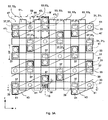
- FIG. 1 a schematic of a prior art MRAM array is shown.
- the MRAM array is arranged in a cross-point architecture, with a magnetic tunnel junction (MTJ) 1 between each intersection of one of a plurality of bit lines 3 and one of a plurality of digit lines 5 arranged perpendicular to the bit lines 3. Therefore, each row of the array is defined by a bit line 3 and each column of the array is defined by a digit line 5.
- MTJ magnetic tunnel junction
- the MTJ 1 is in electrical contact with the bit line 3. However, the MTJ 1 is electrically isolated from the digit line 5 by an insulating matrix 18.
- the MTJ 1 has a magnetic easy axis in the plane of the MTJ 1 (defined herein as the x-y plane) and a magnetic hard axis in the plane of the MTJ 1.
- the magnetic easy axis is defined to be parallel to the x-axis
- the magnetic hard axis is defined to be parallel to the y-axis.
- the bit line 3 is aligned parallel to the easy axis of the MTJ 1 i.e. aligned parallel to the x-axis.
- the digit line 5 is aligned parallel to the hard axis of the MTJ 1 i.e. aligned parallel to the y-axis.
- Each MTJ 1 is disposed on a bottom electrode 7.
- Each bottom electrode 7 is connected to an isolation transistor 9, 9a, 9b.
- Each isolation transistor 9, 9a, 9b is connected to a sense line (not shown).
- Word lines 11 run parallel to the digit lines 5 i.e. parallel to the y-axis. Each word line 11 is connected to the gate of all the transistors 9, 9a, 9b in a single column.
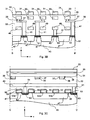
- Figure 2 is a cross-section through two neighbouring memory cells of a row of the MRAM array, taken along the line A-A'.
- Each memory cell 13a, 13b is formed of one transistor 9a, 9b and one MTJ 1a, 1b.
- a source 15 of each isolation transistor 9a,9b is shared between neighbouring cells 13a, 13b.
- a sense line 17 is connected to the source 15 of the isolation transistor 9a, 9b.
- both MTJs 1a, 1b are connected to the bit line 3.
- Each MTJ 1 a, 1b is connected via a respective bottom electrode 7a, 7b to a drain 19a, 19b of the transistor 9a, 9b.
- a word line 11a, 11b is connected to a gate 21a, 21b of each transistor 9a, 9b.
- a digit line 5a, 5b runs underneath each MTJ 1a, 1b. The digit line 5a, 5b is separated from the bottom electrode 7a, 7b by an insulating matrix 18.
- Each MTJ 1a, 1b comprises a free layer 23, a pinned layer 25, and a thin dielectric barrier 27 between the free layer 23 and the pinned layer 25.
- a pinning layer 29 is coupled to the pinned layer 25.
- the free layer 23 is a ferromagnetic layer having a relatively low coercivity.
- the pinned layer 25 is a ferromagnetic layer having a relatively high coercivity.
- the dielectric barrier 27 has a thickness such that electrons can tunnel through it.
- the pinning layer 29 is an antiferromagnetic layer and prevents the magnetisation of the pinned layer 25 from switching.
- the dielectric barrier 27 comprises aluminium oxide (AlO x ) and has a thickness of about 20 ⁇ .
- the free layer 23 and the pinned layer 25 are formed of nickel iron (NiFe).
- the pinning layer 29 can be formed of iron manganese (FeMn) or iridium manganese (IrMn).
- the field H 1 generated by the bit line 3 is about half the field required to switch the magnetisation of the free layer 23.
- the field H 2 generated by the digit line 5a is also about half the field required to switch the magnetisation of the free layer 23.
- the sum of the two magnetic fields H 1 and H 2 is just over the switching threshold of the free layer 23.
- the magnetic field generated around the MTJ 1b is insufficient to cause switching of the free layer 23.
- the magnetic field generated around the MTJ a is sufficient to cause switching of the free layer 23. In this way, only a single MTJ 1a is switched by driving current through the bit line 3 corresponding to the row of the MTJ 1a and through the digit line 5a corresponding to the column of the MTJ 1a.
- the sum of the magnetic fields H 1 and H 2 is insufficient to cause switching of the pinned layer 25.
- a bias is applied to the word line 11a, so that the transistor 9a is switched on. Therefore, current can flow through the MTJ 1a, and current is also able to flow through all the MTJs in the same column of the array. Then, a bias is also applied to the bit line 3. Therefore, current flows through the MTJ 1a in the column defined by the word line 11a and the row defined by the bit line 3.
- the magnetoresistance of the MTJ 1a depends on the direction of magnetisation of the free layer 23.
- the magnetisation of the free layer 23 is arranged parallel to the magnetisation of the pinned layer 25, there is an equal density of states across the dielectric barrier 27 for spin-up and spin-down electrons. This results in a high probability of tunnelling across the barrier 27, resulting in low resistance state.
- the magnetisation of the free layer 23 is arranged anti-parallel to the magnetisation of the pinned layer 25, the density of states across the barrier 27 is not equal for spin-up and spin-down electrons. This reduces the probability of tunnelling across the barrier 27, resulting in a high resistance state.
- the resistance of the memory cell 13a is compared with an associated reference memory cell (not shown) through sense circuitry (not shown). In this way, the state of the memory cell 13a can be determined.
- the size of the above-described memory cell 13a is limited by the available power. This is because, as the size of the MTJ decreases, the coercivity of the free layer 23 increases, increasing the current required through the bit lines 3 and the digit lines 5 to switch the memory cell 13a.
- half-selected MTJs i.e. the MTJs in the column of the selected digit line or row of the selected bit line
- this writing method suffers from a small writing margin due to shape variations in the free layer.
- STT switching MRAMs can reduce the required power for a given cell size.
- the current required for writing in the nano-second regime can be many times larger than the DC threshold current.
- the memory array is a magnetic random access memory (MRAM).
- MRAM magnetic random access memory
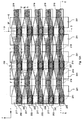
- the memory array is made up of a plurality of word lines 53, defining a first dimension of the array, in this example columns of the array, and a plurality of bit lines 31, overlying and perpendicular to the word lines 53, defining a second dimension of the array, in this example rows of the array.
- a plurality of magnetic tunnel junctions (MTJs) 37 having stacked layers are connected to the underside of each bit line 31, in spaces between the word lines 53.
- MTJs magnetic tunnel junctions
- the bit lines 31 are arranged in a first direction, herein defined as the x-axis.
- the word lines 53 are arranged in a second direction, herein defined as the y-axis
- a plurality of assist current lines 33 are arranged parallel to the x-axis.
- the assist current lines 33 overlie the bit lines 31 and are electrically isolated from the bit lines 31 by an insulating matrix 35.
- each MTJ 37 is formed in a pillar defined by sidewalls 38 and has an elliptical base having a short axis L 1 and a long axis L 2 .
- the pillar has a uniform cross section up its height i.e. a uniform cross section in the x-y plane.
- the difference in length between the long axis L 2 and the short axis L 1 provides magnetic shape anisotropy.
- the ratio of the short axis L 1 length to the long axis L 2 length is 1:2. Therefore, each MTJ 37 has a magnetic easy axis parallel to the long axis, i.e. parallel to the x-axis, and a magnetic hard axis parallel to the short axis, i.e. parallel to the y-axis.
- each MTJ 37 is connected to the underside of a bit line 31.
- the assist current line 33 is above the bit line 31.
- the MTJs 37 are electrically isolated from the assist current lines 33.
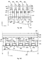
- An underside of each MTJ 37 is connected to a bottom electrode 39.
- a via 41 connects each bottom electrode 39 to an active region 43 in a substrate 45.
- the active regions 43 define areas within which diffusion of charge carriers can occur in the substrate 45.
- the active regions 43 are isolated from one another in the substrate 45 by shallow trench isolation (STI) regions 47.
- STI shallow trench isolation
- a sense line 49 runs parallel to and underneath each bit line 31.
- the sense lines 49 are separated from the bit lines 31, the bottom electrodes 39, and vias 41 by an insulating matrix 50.
- a via 51 connects each active region 43 to the sense line 49 above it.
- the word lines 53 are provided on the substrate 45 and are isolated therefrom by a gate oxide 53a.
- the word lines 53 are arranged perpendicular to the bit lines 31, the assist current lines 33, and the sense lines 49.
- the word lines 53 are separated from the sense lines 49 by an insulating matrix 55.
- MTJs 37 are provided alternately between neighbouring pairs of the word lines 53.
- a first MTJ 37 1 is provided between a first word line (not shown) and a second, adjacent word line 53 2
- a second MTJ 37 2 is provided between third and fourth word lines 53 3 , 53 4
- a third MTJ 37 3 is provided between fifth and sixth word lines 53 5 , 53 6 .
- a fourth MTJ 37 4 is provided between second and third words lines 53 2 , 53 3 , a fifth MTJ 37 5 is provided between fourth and fifth bit lines 53 4 , 53 5 and a sixth MTJ 37 6 is provided between a sixth word line 53 6 and a seventh, adjacent word line (not shown).
- Neighbouring MTJs 37 on each bit line 31 are arranged into pairs 59.
- each pair of MTJs 59 has an active region 43 1 running between the respective vias 41 1 , 41 2 of two MTJs 37a, 37b.
- STI regions 47 separate the active region 43 1 for each pair 59.
- the via 51 1 connecting the active region 43 1 to the sense line 49 is provided between the word lines 53 2 , 53 3 that are in area defined by the pair 59.
- a source region 61 is provided in the active region 43 below each via 41 connecting the bottom electrode 39 to the active region 43.
- a drain region 63 is provided in the active region 43 below each via 51 connecting the sense line 49 to the active region 43. Therefore, each active region 43 provides two source regions 61 and one drain region 63. Conduction between each source region 61 and the drain region 63 occurs through the word line 53 between said regions. Therefore, said word line 53 serves as a gate 65 of an isolation transistor 81, and one isolation transistor 81 is provided for each MTJ 37.
- a memory cell 66 is defined by one MTJ 37 and a respective transistor.
- the drain region 63 of the transistor is shared between neighbouring memory cells 66.
- the memory cell 66 has an area 8F 2 .
- the feature size F of the memory array may be 100 nm or less.
- the separation between the bit line 31 and the assist current line 33 is in the range 20 nm to 100 nm.
- the bit line 31 and the assist current line 33 are made of a conductive material, such as copper or tungsten.
- the insulating matrix 35 is silicon dioxide (SiO 2 ).
- the MTJ 37 comprises a sequence of layers, including a capping layer 82, a free layer 83, a tunnel barrier layer 84, a pinned layer 85, a pinning layer 87, and a buffer layer 89.
- the capping layer 82 is furthest from the substrate 45 and the buffer layer 89 is closest to the substrate 45.
- the free layer 83 is formed magnesium oxide (MgO) and is sufficiently thin that electrons can tunnel through it.
- MgO magnesium oxide
- the pinned layer 85 is a synthetic antiferromagnet (SAF).
- SAF 85 comprises a first ferromagnetic sub-layer 91, having a first magnetisation, and a second ferromagnetic sub-layer 93, having a second magnetisation, separated by an antiferromagnetic layer 95.
- the first magnetisation and the second magnetisation are unequal in magnitude, and are antiparallel to one another.
- the second ferromagnetic sub-layer 93 is a thicker than the first ferromagnetic sub-layer 91, therefore the second magnetisation has a larger magnitude than the first magnetisation.
- the antiferromagnetic layer 95 couples the first ferromagnetic sub-layer 91 and the second ferromagnetic sub-layer 93.
- the first magnetisation and the second magnetisation are aligned parallel to the easy axis of the MTJ 37 i.e. parallel to the x-axis. Therefore, the SAF has a small net magnetisation in the x-direction.
- the pinned layer 85 has a relatively high coercivity.
- the pinning layer 87 comprises an antiferromagnetic material.
- the pinning layer 87 pins the magnetisation of the pinned layer 85, to prevent the magnetisation of the pinned layer 85 from switching on application of a magnetic field or a switching current.
- the MTJ 37 When the magnetisation of the free layer 83 is parallel to the magnetisation of the first ferromagnetic sub-layer 91 of the pinned layer 85, the MTJ 37 has a relatively low magnetoresistance. When the magnetisation of the free layer 83 is anti-parallel to the magnetisation of the first ferromagnetic sub-layer 91 of the pinned layer 85, the MTJ 37 has a relatively high magnetoresistance.
- the capping layer 82 is formed of a non-magnetic metal, for example copper (Cu) or tantalum (Ta), and has a thickness of about 10 nm.
- the capping layer 82 may be formed of two layers of tantalum each having a thickness of 5 nm separated by a layer of copper having a thickness of 10 nm i.e. Ta(5 nm)/Cu(10 nm)/Ta(5 nm).
- the free layer 83 is formed of cobalt iron boron (CoFeB) and has a thickness of about 3 nm.
- the tunnel barrier layer 84 is formed of magnesium oxide (MgO).
- MgO magnesium oxide
- other dielectric materials such as aluminium oxide (AlO x ), silicon dioxide (SiO 2 ), and aluminium nitride (A1N)
- AlO x aluminium oxide
- SiO 2 silicon dioxide
- A1N aluminium nitride
- the tunnel barrier layer 84 has a thickness of 2 nm. In other examples, the thickness of the tunnel barrier layer 84 can be in the range 1 nm to 2 nm.
- the first ferromagnetic sub-layer 91 is formed of cobalt iron boron (CoFeB) and has a thickness of about 4 nm.
- the coupling layer 95 is formed of rubidium (Ru) and has a thickness of about 0.8 nm.
- the second ferromagnetic sub-layer 93 is formed of cobalt iron (CoFe) and has a thickness of about 6 nm.
- the pinning layer comprises platinum manganese (PtMn) and has a thickness of about 15 nm.
- PtMn is preferred because it has a high blocking temperature and a high exchange biasing field, which improve the thermal stability of the MTJ 37.
- other antiferromagnetic materials such as iridium manganese (IrMn), nickel manganese (NiMn) and palladium manganese (PdMn) can be used.
- the buffer layer 89 is formed of at least one non-magnetic conductive layer and has a thickness between 10 nm and 20nm.
- the buffer layer 89 can be formed of two layers of tantalum each having a thickness of 5 nm separated by a layer of copper having a thickness of 10 nm, and an overlying layer of nickel-iron having a thickness of 5 nm separated from the copper layer by one of the tantalum layers i.e. Ta(5 nm)/Cu(10 nm)/Ta(5 nm)/NiFe(5 nm).
- the two tantalum layers may be separated by a gold layer having a thickness of 10 nm i.e.
- the buffer layer 89 may be formed of a layer of tantalum having a thickness of 5 nm and a layer of nickel-iron having a thickness of 5nm i.e. Ta(5 nm)/NiFe(5 nm).
- the nickel-iron layer is a seed layer for the pinning layer 87.
- the long and short axes of the elliptical cross section of the MTJ 37 in the x-y plane have dimensions 100 nm and 50 nm respectively.
- the ratio of magnetoresistance for the relatively high resistance state and the relatively low resistance state can approach 3:1 for the above-described MTJ 37. This can provide an MRAM having a high signal to noise ratio.
- the assist current line 33 and the free layer 83 are separated by a distance dependent upon the anisotropy magnetic field of the free layer 83, and the current through the assist current line 33.
- the anisotropy magnetic field can be determined by measuring the hysteresis loop of the free layer 83 when a magnetic field is applied to the magnetic hard axis of the free layer 83.
- the magnitude of the assist magnetic field may be one tenth of the anisotropy magnetic field.
- the anisotropy magnetic field of the free layer 83 is typically 300 to 400 Oe. Therefore, the assist magnetic field is 30 to 40 Oe.
- H A the assist magnetic field
- I A the current in the assist current line 33
- r the distance between the assist current line 33 and the free layer 83.
- the maximum current density that can be provided by a copper wire is of the order of 10 6 A/cm 2 .
- I A is of the order of 10 -10 A.
- the distance between the assist current line 33 and the MTJ 37 is of the order of 100 nm.
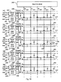
- control circuitry for the memory array is shown.
- a write driver 67 and a sense amplifier 68 are provided for each row of the memory array.
- Each bit line 31 is connected to a first output 69 of a respective write driver 67.
- Each sense line 49 is connected to a second output 70 of the respective write driver 67.
- Each bit line 31 is also connected to a first input/output port 71 of the respective sense amplifier 68.
- a connection 72 is provided between a second output of the sense amplifier 68 and a first input of the respective write driver 67.
- the write driver 67 has a second input 73 for applying a write amplifier enable (WAE) voltage.
- WAE write amplifier enable
- the sense amplifier 68 has a second input 74 for receiving a sense amplifier enable (SAE) voltage.
- the sense amplifier 68 has a third input/output port 75 for applying a sense amplifier input/output (SAIO) voltage.
- An assist driver 78 is provided for each row of the array.
- Each assist driver 78 has a first input connected to an assist current line 33.
- a single word line driver 80 is provided. Each word line 53 is connected to a respective output of word line driver 80.
- Each MTJ 37 connects a bit line 31 to the sense line 49 in the same row, through a single isolation transistor 81.
- the base of the isolation transistor 81 is connected to a single word line 53.
- Current will flow through the MTJ 37 when a bias is applied to the word line 53 defining the column of the MTJ 37, and a bias is applied to the bit line 31 or sense line 49 defining the row of the MTJ 37.
- each MTJ 37 is addressable by a single word line 53 and a single bit line 31 or sense line 49.
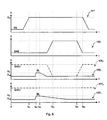
- Figure 6 illustrates biases which are applied to and measured in the memory array during a read cycle.
- a first plot 101 is of a word line bias against time.
- a second plot 103 is of a sense amplifier enable (SAE) bias applied to the second input 74 of the sense amplifier 68 against time.
- a third plot 105 1 and a fourth plot 105 2 are of the voltage response on the bit line 31 against time and the sense amplifier input/output (SAIO) bias against time respectively, when the magnetisation of the free layer 83 and the magnetisation of the pinned layer 85 are parallel.
- a fifth plot 107 1 and a sixth plot 107 2 are of the voltage response on the bit line 31 against time and the SAIO bias against time respectively, when the magnetisation of the free layer 83 and the magnetisation of the pinned layer 85 are antiparallel.
- V W is applied by the word line driver 80 to the word line (WL) 53 corresponding to the column of the memory cell 66.
- V W may be in the range 1 V to 3 V. This opens the isolation transistors 81 in the column of the array.
- a bias V B is applied by the write driver 67 to the bit line (BL) 31 corresponding to the row of the memory cell.
- V B is about 0.4 V.
- the sense line (SL) 49 corresponding to the row of the memory cell is held a ground.
- the bias V B is removed.
- the voltage response on the bit line 31 decreases to ground in about 1 ns. This is because, when the magnetisation of the free layer 83 and the magnetisation of the pinned layer 85 are parallel, the magnetoresistance of the MTJ 37 (and thus the measured voltage response) is relatively low, thus the voltage response is relatively fast.
- the voltage response on the bit line 31 decreases to ground in about 2 to 3 ns. This is because, when the magnetisation of the free layer 83 and the magnetisation of the pinned layer 85 are anti-parallel, the magnetoresistance of the MTJ 37 (and thus the measured voltage response) is relatively high, thus the voltage response is relatively slow.
- V ref may be about 0.5 V B . In this example, V ref is 0.2V.
- the sense amplifier input/output (SAIO) at the third input/output port 75 of the sense amplifier 68 is set to be low.
- t R1 is 1 ns
- t R2 is 2.5 ns
- t R3 is 3.5 ns
- t R4 is 7.5 ns
- t R5 is 9 ns
- t R6 is 10 ns.
- the direction of magnetisation of the free layer 83 determines the output of the third input/output port 75 of the sense amplifier 68. If the free layer 83 is parallel to the pinned layer 85, the output of the sense amplifier 68 is '0'. If the free layer 83 is anti-parallel to the pinned layer 85, the output of the sense amplifier 68 is '1'.
- Figure 7 illustrates biases which are applied to the memory array during a write cycle.
- a seventh plot 109 is of an assist current line (AL) bias against time.
- An eighth plot 111 is of a word line (WL) bias against time.
- a ninth plot 113 is of a write amplifier enable (WAE) bias against time.
- a tenth plot 115 and an eleventh plot 117 are of an SAIO bias applied to the memory cell 66 against time and of biases applied to the bit line (BL) and sense line (SL) against time respectively, when the magnetisation of the free layer 83 switches from anti-parallel to the magnetisation of the pinned layer 85 to parallel to the magnetisation of the pinned layer 85 (AP to P switching).
- a twelfth plot 119 and a thirteenth plot 121 are of an SAIO bias applied to the memory cell 66 against time and of biases applied to the bit line (BL) and sense line (SL) against time respectively, when the magnetisation of the free layer 83 switches from parallel to the magnetisation of the pinned layer 85 to antiparallel to the magnetisation of the pinned layer 85 (P to AP switching).
- V A is applied by the assist driver 78 to the assist current line 33 that corresponds to the row of the memory cell 66.
- the magnitude of V A is chosen to provide the required assist magnetic field in the free layer 83. A value of V A can be found by routine experiment.
- V W is applied by the word line driver 80 to the word line 53 that corresponds to the column of the memory cell 66.
- V W may be in the range 1V to 3V. This opens the isolation transistors 81 in the column of the array.
- the SAIO bias is applied to the third input/output port 75 of the sense amplifier 68 corresponding to the row of the memory cell 66.
- the SAIO bias is held at ground.
- the SAIO bias is held at V S .
- the connection 72 transmits this signal from the second output of the sense amplifier 68 to the first input of the write driver 67.
- the WAE bias is applied to the write driver 67 corresponding to the row of the memory cell 66. This enables the write driver 67 to apply a bias to either the bit line 31 or the sense line 49, depending on the output SAIO of the sense amplifier 68.
- the write driver 67 when SAIO is held at ground, at time t W3 the write driver 67 applies a bias V B to the bit line 31, and the sense line 49 is held at ground. Therefore, the write driver 67 drives current from the sense line 49 to the bit line 31. This causes the free layer 83 to switch from AP to P.
- the write driver 67 when SAIO is held at V S , at time t W3 the write driver 67 applies a bias V B to the sense line 49, and the bit line 31 is held at ground. Therefore, the write driver 67 drives current from the bit line 31 to the sense line 49. This causes the free layer 83 to switch from P to AP.
- V B may be in the range 1 V to 1.5 V, and has approximately the same value for P to AP switching as for AP to P switching.
- the AL bias is removed.
- the BL or SL bias is removed.
- the WL bias is removed.
- t W1 is 1 ns
- t W2 is 2 ns
- t W3 is 3 ns
- t W4 is 4 ns
- t W5 is 8 ns
- t W6 is 9 ns
- t W7 is 10 ns.
- Figures 8A and 8B illustrate the current I A through the assist current line 33 ( Figure 4 ) and the current I MTJ through the MTJ 37 ( Figure 4 ) at times of the write cycle for AP to P switching and P to AP switching respectively.
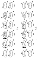
- Figures 9A and 9B illustrate magnetisations M 1 , M 2 of the free layer 83 at times of the write cycle for AP to P switching and P to AP switching respectively.
- I A1 may be of the order of 100 ⁇ A.
- the current I A in the assist current line 33 is held at I A1 between time t W2 and t W4 .
- the current I A induces an assist magnetic field H A in the free layer 83.
- the magnetic field H A is parallel to the magnetic hard axis of the free layer 83.
- application of the field H A causes the magnetisation M 1 of the free layer 83 to rotate anticlockwise by an angle ⁇ in the plane of the free layer 83.
- the current I MTJ in the MTJ 37 is ramped up to a magnitude I MTJ1 .
- the current I MTJ in the MTJ 37 is held at I MTJ1 between time t W3 and t W6 .
- the current I MTJ flows from the free layer 83 to the pinned layer 85. Therefore, electrons that are spin-polarised by the pinned layer 85 are injected into the free layer 83.
- the spin transferred by these electrons causes precession of the magnetisation M 1 of the free layer 83 about a precession axis P 1 . Therefore, the magnetisation M 1 rotates around the precession axis P 1 .
- the precession axis P 1 and therefore the time average of the magnetisation M 1 , is rotated further anticlockwise in the plane of the free layer 83. This rotation is assisted by the magnetic field H A .
- the magnetisation M 1 of the free layer 83 continues to rotate around the precession axis P 1 .
- the precession axis P 1 of the magnetisation M 1 is perpendicular to the initial direction of the magnetisation M 1 i.e. it is parallel to the magnetic hard axis of the free layer 83 and to the assist magnetic field H A .
- the angle of the magnetisation M 1 around the precession axis P 1 gradually increases, and the precession axis P 1 suddenly rotates further anticlockwise
- the current I MTJ still causes the precession axis P 1 to rotate clockwise. Therefore, it is preferable that the assist current I A is removed so that it does not act to prevent the precession axis P 1 rotating further anticlockwise.
- the current I A in the assist current line 33 is ramped down to zero.
- the assist current I A is zero, therefore there is no assist magnetic field H A .
- the switching current I MTJ remains, causing the precession axis P 1 of the magnetisation M 1 of the free layer 83 to rotate further anticlockwise.
- the current I A in the assist current line 33 is ramped up to a magnitude I A2 .
- the current I A2 has the same magnitude as A1 , but is in the opposite direction.
- the current I A in the assist current line 33 is held at I A2 between time t W2 and t W4 .
- the current I A induces an assist magnetic field H A in the free layer 83.
- the magnetic field H A is parallel to the magnetic hard axis of the free layer 83.
- application of the field H A causes the magnetisation M 1 of the free layer 83 to rotate anticlockwise by an angle ⁇ in the plane of the free layer 83.
- the current I MTJ in the MTJ 37 is ramped up to a magnitude I MTJ2 .
- the current I MTJ in the MTJ 37 is held at I MTJ2 between time t W3 and t W6 .
- I MTJ2 has approximately the same magnitude as I MTJ1 .
- the current I MTJ flows from the pinned layer 85 to the free layer 83. Therefore, spin-polarised electrons are scattered from the pinned layer 85 and injected into the free layer 83. The spin transferred by these electrons causes precession of the magnetisation M 1 of the free layer 83. Therefore, the magnetisation M 1 rotates around the precession axis. The precession axis P 1 , and therefore the time average of the magnetisation M 1 , is rotated further anticlockwise in the plane of the free layer 83. This rotation is assisted by the magnetic field H A .
- the magnetisation M 1 of the free layer 83 continues to rotate around the precession axis P 1 .
- the precession axis P 1 of the magnetisation M 1 is perpendicular to the initial direction of the magnetisation M 1 i.e. it is parallel to the magnetic hard axis of the free layer 83 and to the assist magnetic field H A .
- the angle of the magnetisation M 1 around the precession axis P 1 gradually increases, and the precession axis P 1 suddenly rotates further anticlockwise.
- the current I MTJ still causes the precession axis P 1 to rotate anticlockwise. Therefore, it is preferable that the assist current I A is removed so that it does not act to prevent the precession axis P 1 rotating further anticlockwise.
- the current I A in the assist current line 33 is ramped down to zero.
- the assist current I A is zero, therefore there is no assist magnetic field H A .
- the switching current I MTJ remains, causing the precession axis P 1 of the free layer 83 to rotate further clockwise.
- the current required to cause STT switching is related to the duration of the current pulse, as described above, and to the initial direction of the magnetisation of the free layer 83.
- the assist current I A can be applied before the STT switching current I MTJ , to rotate the magnetisation of the free layer and thus lower the STT switching current.
- the leading or rising edge of the assist current line bias occurs before the leading or rising edge of the bit line or sense line bias and the trailing or falling edge of the assist current line bias occurs after the leading or rising edge of the bit line bias or sense line bias.
- the assist current I A is switched off during the STT switching process. This is because if the assist magnetic field H A is present after STT switching ends, the domain structure of the free layer 83 becomes unstable. This causes an increase in the probability distribution of the STT switching current in the nanosecond regime, and a narrow current margin for the STT writing process. Therefore, in this example the trailing or falling edge of the assist current line bias occurs before the trailing or falling edge of the bit line or sense line bias.
- the direction of the assist magnetic field H A can be aligned in either of two directions parallel to the magnetic hard axis of the free layer 83depending on the direction of the switching current I MTJ .
- the switching current I MTJ induces an Ampere field in the free layer 83 and aligning the assist magnetic field H A to eliminate the Ampere field in the free layer 83 can result in a more favourable (e.g. more stable) domain structure in the free layer 83 for STT switching. Therefore, the assist magnetic field H A for AP to P switching can be arranged to be in the opposite direction to the assist magnetic field H A for P to AP switching.
- the effect of the Ampere field is not significant, and so the assist magnetic field H A can be aligned in the opposite direction, i.e. without counteracting the Ampere field, for STT switching.
- the switching current can be reduced further.
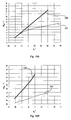
- FIGS. 10A and 10B respective simulation results for STT switching with and without an assist magnetic field are shown.
- the simulation is of STT switching at a temperature of 300K, using a spin-polarised current having a polarisation of 0.5.
- the simulation results show normalised current I/I c0 -1 required for STT switching against the inverse of the pulse duration t p -1 .
- a switching current 127 for a given pulse duration when an assist magnetic field pulse of magnitude 80 Oe is used can be up to 50% less than a switching current 129 when no assist magnetic field is used.
- a switching current 131 for a given pulse duration when an assist magnetic field pulse of magnitude 80 Oe is used can be up to 100% less than a switching current 133 when no assist magnetic field is used.
- Figures 11A, 11C , 11E and 11G show a cross section of the memory array shown in Figure 3A taken along line B-B' during stages of the fabrication process.
- Figures 11B, 11D , 11F and 11H show a cross section of the Figure 3A memory array taken along line C-C' during stages of the fabrication process.
- an STI etch process is used to create shallow trenches 47 in the silicon substrate 45, which are filled with dielectric material. Areas of the substrate that do not comprise the STI regions define the active regions 43.
- Gate insulating layers 53a and word lines 53 are sequentially stacked to form gate stacks on the substrate and STI regions.
- Gate spacers 53b are formed on the sidewalls and on top of the gate stack.
- Impurity ions are implanted into the substrate 45 to form source region 61 and drain regions 63 for isolation transistors.
- a first insulating matrix 55 is formed on the entire surface of the substrate.
- the first insulating matrix 55 is successively patterned and etched to open vias 51 that expose a portion of each drain region 63.
- One or more conductive layers are then formed on the substrate and fill the vias 51.
- the upper portion of the conductive layer is then removed, typically using a planarisation process, to remove all of the conductive layer except that formed in the vias 51, and expose a top surface of the first insulating matrix 55.
- Another conductive layer is then formed on the first insulating matrix 55.
- the conductive layer is patterned then etched to form sense lines 49 running perpendicular to the word lines and contacting the conductive layer in the via 51.
- a second insulating matrix 50 is then formed on the structure.
- vias 41 are formed in the first insulating matrix and the second insulating matrix to contact the surface of each source region 61.
- a conductive layer is formed on the substrate.
- the conductive layer is then patterned and etched to form bottom electrodes 39 contacting vias 41.
- the MTJs 37 are then fabricated according to the following steps.
- the buffer layer 89 and the antiferromagnetic pinning layer 87 are deposited in series.
- the magnetisation of the pinning layer 87 is set by heating it and applying an external magnetic field to it, which is maintained as the pinning layer 87 cools.
- the first ferromagnetic sub layer 91, antiferromagnetic coupling layer 95 and second ferromagnetic sub-layer 93 are then deposited in series over the pinning layer 87.
- the barrier material is then deposited.
- The can be achieved by r-f sputtering the material, or depositing magnesium and then oxidising the magnesium by a process such as plasma oxidation.
- the ferromagnetic free layer 83 is then deposited.
- the capping layer 82 is deposited on the ferromagnetic free layer 83.
- Patterning may be performed by depositing a layer of photoresist on the protective capping layer, using photolithography to pattern the photoresist, and removing the unprotected material.
- a third insulating matrix 123 is then formed over the upper surface of the substrate including the MTJ 37.
- the third insulating matrix 123 is patterned to form a bit line contact holes 125 that exposes the surfaces of the capping layers 82.
- a conductive layer is then formed on the substrate and in bit line contact holes 125.
- the conductive layer is then patterned and etched to form bit lines 31 that cover the bit line contact holes 125, and are parallel to the sense lines 49.
- a fourth insulating matrix 35 is formed on the entire surface of the substrate.
- a conductive layer is formed on the substrate, and is subsequently patterned and etched to form assist current lines 33 above and parallel to the bit lines 31.
- the conductive layers can be formed using a method well known in the art such as chemical vapour deposition, physical vapour deposition, plasma enhanced chemical vapour deposition, or sputtering.
- the memory array is an MRAM.
- bit lines 201 are arranged in a first direction, herein defined as the x-axis.
- the bit lines 201 define a first dimension of the array, in this example, rows of the array.
- An assist current line 203 overlies each bit lines 201, and is electrically isolated from the respective bit line 201 by an insulating matrix 205.
- a plurality of MTJs 207 are provided.
- the MTJs 207 have the same structure as the MTJs 37 described above with respect the first example.
- the MTJs 207 are arranged with the magnetic easy axis parallel to the bit lines 201, i.e. parallel to the x-axis.
- Each MTJ 207 is connected to the underside of a bit line 201.
- the MTJs 207 are electrically isolated from the assist current lines 203.
- each MTJ is connected to a bottom electrode 209.
- the bottom electrode 209 is a rectangle in the x-y plane having long and short sides.
- the long and short sides of the bottom electrode 209 are approximately the same size as the long and short axes of the MTJ 207.
- a via 211 connects each bottom electrode 209 to an active region 213 on a substrate 215.
- the active regions 213 are electrically isolated from one another on the substrate 215 by STI regions 216.
- a sense line 217 runs underneath each bit line.
- the sense line 217 does not contact the bit lines 201, the MTJs or the bottom electrodes 209.
- a via 219 connect the sense line 217 to the active region 213.
- each sense line 217 weaves side to side about a longitudinal axis.
- the longitudinal axis is parallel to the x-axis.
- Each active region 213 also weaves side to side about a longitudinal axis that is parallel to the x-axis.
- the pitch of the weave of the sense line 217 is the same as the pitch of the weave of the active region 213.
- the weaves are 180° out of phase such that the weave of the sense line 217 and the weave of the active layer 213 coincide at and are contacted by vias 219.
- the vias 211 connecting the bottom electrodes 209 to the active region 213 are provided. Therefore, the sense line 217 is spaced apart from the vias 211 connecting the bottom electrode 209 to the active region 213.
- a plurality of word lines 221 are provided on the substrate 215 and are isolated therefrom by a gate oxide 221a.
- the word lines 221 are perpendicular to the bit lines 201.
- the word lines 221 are arranged in a second direction, herein defined as the y-axis.
- the word lines 221 are isolated from the sense lines by an insulating matrix 223.
- Each word line 221 is provided between the vias 219 connecting the sense line 217 to the active region 213 and the vias 211 connecting the bottom electrode 209 to the active region 213.
- the word lines 221 define a second dimension of the array, in this example, columns of the array. Two word lines 221 are provided for each MTJ 207.
- each column of the array is defined by the two word lines 221 on either side of a column of MTJs 207.
- a source region 227 is provided in the active region 213 below each via 211 connecting the bottom electrode 209 to the active region 213.
- a drain region 229 is provided in the active region 213 below each via 219 connecting the sense line 217 to the active region 213. Conduction between each source region 227 and the drain region 229 occurs through the word line 221 between said regions. Therefore, said word line 221 serves as a gate 231 of an isolation transistor 233.
- each memory cell 235 is defined by one MTJ 207 and two transistors 233.
- the drain region 229 of each transistor 233 is shared between neighbouring memory cells 235.
- the area of each memory cell 235 is 8F 2 .
- the feature size F of the memory array is between 50 nm and 100 nm.
- control circuitry for the memory array is shown.
- a write driver 236 and a sense amplifier 237 are provided for each row of the memory array.
- Each bit line 201 is connected to a first output 238 of the respective write driver 236.
- Each sense line 217 is connected to a second output 239 of the respective write driver 237.
- Each bit line 201 is also connected to a first input/output port 240 of the respective sense amplifier 237.
- a connection 241 is provided between a second output of the sense amplifier 237 and a first input of the respective write driver 236.
- the write driver 236 has a second input 242 for applying a write amplifier enable (WAE) voltage.
- WAE write amplifier enable
- the sense amplifier 237 has a second input 243 for applying a sense amplifier enable (SAE) voltage.
- the sense amplifier 237 has a third input/output port 244 for applying a sense amplifier input/output (SAIO) voltage.
- An assist driver 246 is provided for each row of the array. Each assist driver 246 has a first input connected to an assist current line 203.
- a single word line driver 245 is provided. Each word line 221 is connected to a respective output of word line driver 245.
- Each MTJ 207 connects a bit line 201 to the sense line 217 in the same row, through one of two isolation transistors 233 either side of the MTJ 207.
- the base of each isolation transistor 233 is connected to a single word line 221.
- Current will flow through the MTJ 207 when a bias is applied to both of the word lines 221 defining the column the memory cell 235, and a bias is applied to the bit line 201 or sense line 203 defining the row of the MTJ 207.
- each MTJ 207 is addressable by two word lines 221 and a single bit line 201 or sense line 217.
- Reading and writing of the memory cell shown in Figures 12A to 12C is the same as that described earlier with respect to the memory cell shown in Figures 3A to 3D .
- FIG. 14 a cross section of an alternative MTJ 247 taken through the x-z plane is shown.
- the MTJ 247 can be used instead of MTJ 37 in the first example or MTJ 207 in the second example.
- the MTJ 247 comprises a sequence of layers, including a free layer 249, a tunnel barrier layer 251, and a pinned layer 253.
- the free layer is furthest from the substrate and the pinning layer is closest to the substrate.
- the free layer 249 comprises a ferromagnetic material.
- the free layer 249 has a relatively low coercivity, so that it can be switched on application of a switching current or magnetic field.
- the tunnel barrier layer 251 is formed of an insulating material, such as magnesium oxide (MgO), and is sufficiently thin that electrons can tunnel through it.
- MgO magnesium oxide
- the pinner layer 253 comprises a ferromagnetic material.
- the pinned layer 253 is thicker than the free layer 249. This provides it with a higher coercivity than the free layer 249. Therefore, the free layer 249 is able to switch upon the application of the switching current and assist magnetic field, and the pinned layer 253 is not able to switch upon application of the switch current and assist magnetic field.
- MTJ 255 a cross section in the x-z plane of another alternative MTJ 255 is shown.
- the MTJ 255 can also be used instead of the MTJ 37 in the first example or the MTJ 207 in the second example.
- the MTJ 255 comprises a sequence of layers, including a free layer 257, a tunnel barrier layer 259, a pinned layer 261, and a pinning layer 263.
- the free layer is furthest from the substrate and the pinning layer is closest to the substrate.
- the free layer 257 comprises a ferromagnetic material.
- the free layer 257 has a relatively low coercivity, so that it can be switched on application of a switching current or magnetic field.
- the tunnel barrier layer 259 is formed of an insulating material, such as magnesium oxide (MgO), and is sufficiently thin that electrons can tunnel through it.
- MgO magnesium oxide
- the pinner layer 261 comprises a ferromagnetic material.
- the pinned layer 261 has a relatively high coercivity, so that it is not switched on application of a switching current or magnetic field.
- the pinning layer 263 comprises an antiferromagnetic material.
- the pinning layer 263 pins the magnetisation of the pinned layer 261, to prevent the magnetisation of the pinned layer 261 from switching on application of a magnetic field or a switching current.
- the alternative MTJs 247, 255 have the advantage of a simpler structure than the MTJ 37 used in the first example and the MTJ 207 used in the second example. Therefore, the alternative MTJs 247,255 are simpler to fabricate. However, the alternative MTJs 247, 255 do not exhibit a magnetoresistance ratio has high as that exhibited as the MTJ 37 and the MTJ 207.
- an assist magnetic field H A can be used to lower the current I MTJ needed to switch the magnetisation M 1 ( Figures 9A & 9B ) in the free layer 83 ( Figures 9A & 9B ).
- the switching current I MTJ can be reduced further if the assist field H A ( Figures 9A & 9B ) is turned on at the same time or shortly before (e.g. no more than about 5 ns) the switching current is turned on. As will be explained in more detail later, even for modest assist fields (e.g. 80 Oe or more), if the current is switched on sufficiently soon after the assist field is switched on, then the switching current can be reduced below the dc threshold current, I c0 .
- the angle ⁇ between the magnetization M 1 and the easy axis 267 of the free layer reaches about 2 ⁇ 0 .
- motion of the magnetization M 1 is damped until it becomes is aligned with the axis 265.
- t press is about 250 ps.
- the Landau-Lifshitz-Gilbert damping constant ⁇ (usually referred to simply as the "damping constant") can be found by routine experiment.
- a resonance curve of magnetic susceptibility can be obtained for a sample of material forming the free layer by exciting the sample using microwaves, while applying a magnetic field and measuring (e.g. transmitted or reflected) microwave intensity.
- spin transfer torque is large during the initial period after the assist field H A is turned on. Therefore, if the STT switching current is turned on during this initial period before precessional motion of the magnetisation M 1 has been damped (i.e. ⁇ t ⁇ t damp ), preferably such that the STT switching current has finished rising before the end of the initial period, then spin transfer torque can be very effective.
- the assist current I A is switched off to help stabilize motion of the magnetization M 1 after STT switching. After the STT switching process ends, the STT switching current is also switched off.
- the STT switching current and its distribution can be reduced below half of that when the assist magnetic field H A is not used.
- t W6 9 ns
- t W7 10 ns.
- time interval ⁇ t to achieve precession-enhanced switching can be less than or greater than 5 ns depending on the values for t precess and t damp and that the time interval is approximately equal to the damping time, i.e. ⁇ t ⁇ t damp > t precess .
- the time interval ⁇ t between turning on the assist current and the switching current can be defined using the feet (e.g. which can be defined as 10% of the maximum value) or the shoulders (e.g. which can be defined as 90 % of the maximum value) of the assist and switching currents. As shown in Figures 8A and 8B , in this embodiment, the feet of the assist and switching currents are used to define the time interval ⁇ t.
- the required current I pusle for switching decreases as the assist field H A increases.
- the results shown in Figure 17 indicate that the small amplitude approximation used to derive equation 1 above is not available for STT switching under these conditions (i.e. ⁇ t ⁇ ⁇ damp ) .
- the anisotropy field of the free layer H k is about 800 Oe.
- an assist current I A of a few hundred ⁇ A can generate an assist field H A of about one hundred Oe which is large enough to reduce the switching current below I c0 .
- the process also helps to reduce the probability distribution of switching in the nanosecond regime.
- a cause of intrinsic probability distribution in the switching current is the distribution of the initial magnetization direction of the free layer due to the thermal fluctuation.
- the assist magnetic field helps to fix the direction of the magnetization of the free layer. Therefore, by using an assist magnetic field pulse, the distribution of the switching current can be reduced. This can help to widen the writing current margin in MRAMs.
- the rise times (e.g. t W1 and t W3 - t W2 ) should be as short as possible, for example a few hundred pico-seconds or less.
- the MTJ is provided with an additional ferromagnetic layer overlying the free layer.
- the additional ferromagnetic layer is separated from the ferromagnetic layer by a non-magnetic conductor.
- the additional ferromagnetic layer can increase the proportion of spin-polarised electrons injected into the free layer when current flows from the pinned layer to the free layer.
- a spin valve is provided instead of an MTJ.
- the spin valve comprises a sequence of layers, including a ferromagnetic free layer and a ferromagnetic pinned layer separated by a nonmagnetic conductor.
- the strength and width of the assist current pulse can be adjusted depending on the magnetic properties of the free layer.
- the orientation of the MTJs with respect to the bit line and sense line can be varied.
- the assist current line should be parallel to the magnetic easy axis of the MTJs.
Description
- The present invention relates to a magnetic memory device and in particular, although not exclusively, to a magnetic random access memory. The present invention relates also to a method of writing to a magnetic memory device.
- The emergence of magnetic random access memory (MRAM) is a promising step for the development of both long-term and short-term data storage. MRAM has the benefit of being non-volatile, while having a lower energy consumption and faster read and write time than Flash memory. MRAM also has a lower energy consumption than the commonly used volatile memories dynamic RAM (DRAM) and static RAM (SRAM), with a read and write time faster than that of DRAM.
- A conventional MRAM cell comprises a magnetic element having a ferromagnetic free layer and a ferromagnetic pinned layer, separated by a non-magnetic layer. The pinned layer has a relatively high coercivity, so that its magnetisation remains fixed upon the application of a writing magnetic field. The free layer has a relatively low coercivity, so that its magnetisation can be changed upon application of the writing magnetic field.
- To write to the MRAM cell, the writing magnetic field is applied to switch the magnetisation of the free layer to be either parallel or anti-parallel to the pinned layer. The free layer exhibits magnetic hysteresis, thus its magnetisation remains unchanged when the magnetic field is removed. This results in a non-volatile memory.
- To read the state of the MRAM cell, a small current is driven through the magnetic element. The magnetoresistance of the magnetic element will be higher when the magnetisations of the free layer and the pinned layer are antiparallel, than when the magnetisations of the free layer and the pinned layer are parallel. In this way, the state of the magnetic element can be determined by measuring its resistance.
- A conventional MRAM is described in "Recent Developments in Magnetic Tunnel Junction MRAM" by S. Tehrani et al., p.2752-2757, IEEE Transactions on Magnetics, Vol. 36, No. 5 (September 2000).
- Such a conventional MRAM suffers from the disadvantage that as the size of the MRAM cell decreases, the magnetic field required to switch the magnetisation of the free layer increases. Therefore, the power consumption of the device increases as the cell size decreases.
- Another technique used to write to a magnetic element is spin-transfer-torque (STT) switching. STT switching is described in "Current-driven Excitation of Magnetic Multilayers" by J.C. Slonczewski, p.9353, Phys. Rev. B, Vol. 54 (1996). To switch the magnetisation of the free layer, instead of applying a magnetic field, a current is driven through the magnetic element perpendicular to the plane of the free and pinned layers. This can result in the injection of spin-polarised electrons into the free layer, either by electrons flowing through the pinned layer, when current is driven from the free layer to the pinned layer, or by electrons scattering from the
pinned layer 85, when current is driven from the pinned layer to the free layer. - When spin polarised electrons are injected into the free layer, their spin angular momentum interacts with the magnetic moments in the free layer. The electrons transfer a portion of their angular momentum to the free layer. This results in switching the magnetisation of the free layer when the spin-polarised current is large enough. -
- An MRAM utilising STT switching is described in "Highly scalable MRAM using field assisted current induced switching" by W.C. Jeong et al., p.184, 2005 Symposium on VLSI Technology Digest of Technical Papers.
- The current required for STT switching decreases as the cell size decreases. Therefore, high density MRAM can be realised with STT switching. For DC current, the threshold current density for STT switching depends on material constants such as the saturation magnetisation, Gilbert's damping constant, and the spin polarisations of both the pinned and free layers. However, the required current for a nano-second pulse is much larger than the DC threshold current. It has been shown that the required current in the nano-second regime is given by

where C is a constant, and Ic0 is the DC threshold current. According to equation (1) above, the current required to switch the magnetisation for a 1ns pulse is four times the DC threshold current. Therefore, STT switching MRAMs having a fast write time will have large power consumption. - Another MRAM is described in "A Novel Non-volatile Memory with Spin Torque Transfer Magnetization Switching: Spin-RAM" by M. Hosomi et al., p19.1, IEEE International Electron Device Meeting 2005 also shows that the current required for STT switching increases significantly in the nano-second regime.
- "Magnetization switching by spin torque using subnanosecond current pulses assisted by hard axis magnetic fields" by T. Devolder et al., Appl. Phys. Lett., 88, pp.152502 (2006) describes an experiment conducted using a pillar-shaped spin valve in which magnetisation switching is induced by spin transfer using nano-second current pulses combined with a fixed hard axis field.
-
US-B-6639830 describes switching a memory cell by driving a current through the memory cell and driving currents through word and bit lines or additional lines to generate a magnetic field in alignment with the direction of the hard axis of a ferromagnetic soft layer, followed by a magnetic field in alignment with the direction of the easy axis of the ferromagnetic soft layer. - The present invention seeks to provide an improved method of operating a magnetic memory device, and is defined by
independent claim 1. - According to a first aspect of the present invention there is provided a method of operating a magnetic memory device, the magnetic memory device comprising first and second leads, a magnetoresistive multilayer structure arranged between said leads, said multilayer structure exhibiting a first, relatively high resistance state and a second, relatively low resistance state, said multilayer structure including a ferromagnetic layer having a magnetic hard axis and a magnetic easy axis, and said multilayer structure being switchable between said first and second states, and a magnetic field source for controllably applying a magnetic field along the magnetic hard axis in the ferromagnetic layer independently of current flow through the multilayer structure for assisting switching of the multilayer structure between first and second states, said method comprising turning on a magnetic field along the magnetic hard axis in the ferromagnetic layer using the magnetic field source and turning on a current through the magnetoresistance multilayer structure within 0 to 5 ns after turning on the magnetic field.
- According to a preferred aspect of the present invention there is provided a method of operating a magnetic memory device, the magnetic memory device comprising first and second leads, a magnetoresistive multilayer structure arranged between said leads, said multilayer structure exhibiting a first, relatively high resistance state and a second, relatively low resistance state, said multilayer structure including a ferromagnetic layer having a magnetic hard axis and a magnetic easy axis, and said multilayer structure being switchable between said first and second states, and a magnetic field source for controllably applying a magnetic field along the magnetic hard axis in the ferromagnetic layer independently of current flow through the multilayer structure for assisting switching of the multilayer structure between first and second states, said method comprising turning on a magnetic field along the magnetic hard axis in the ferromagnetic layer using the magnetic field source and turning on a current through the magnetoresistance multilayer structure within a time Δt, such that Δt < tdamp, where:

where α is a Gilbert damping constant and f is a frequency of precession caused by turning on the magnetic field. - This can allow an even lower switching current through the magnetoresistive multilayer structure to be used.
- The method may comprise turning on a current through the magnetoresistance multilayer structure within 0 to 3 ns or between 0 and 2 ns after turning on the magnetic field.
- According to another preferred aspect of the present invention there is provided a memory comprising: a magnetic memory device comprising: first and second leads; a magnetoresistive multilayer structure arranged between said leads, said multilayer structure exhibiting a first, relatively high resistance state and a second, relatively low resistance state, said multilayer structure including a ferromagnetic layer having a magnetic hard axis and a magnetic easy axis; and a magnetic field source for controllably applying a magnetic field along the magnetic hard axis in the ferromagnetic layer independently of current flow through the multilayer structure for assisting switching of the multilayer structure between first and second states; and circuitry for controlling the magnetic memory device configured to perform the method.
- Embodiments of the present invention will now be described, by way of example, with reference to
Figures 3A to 18 of the accompanying drawings in which: -
Figure 1 is a schematic of a prior art magnetic random access memory (MRAM) array; -
Figure 2 is a cross-section of two neighbouring prior art MRAM cells taken along a line A-A'; -
Figure 3A is a plan view of a memory array comprising an example of a magnetic memory device; -
Figure 3B is a cross section of the memory array shown inFigure 3A taken along a line B-B'; -
Figure 3C is a cross section of the memory array shown inFigure 3A taken along a line C-C'; -
Figure 3D is a side view of part of the memory array shown inFigure 3A ; -
Figure 4 is a cross section of a magnetic tunnel junction used in the memory array shown inFigure 3A ; -
Figure 5 illustrates control circuitry for the memory array shown inFigure 3A ; -
Figure 6 illustrates biases which are applied to the memory array shown inFigure 3A during a read cycle; -
Figure 7 illustrates biases which are applied to the memory array shown inFigure 3A during a write cycle; -
Figures 8A and 8B illustrates current through the memory array shown inFigure 3A during a write cycle; -
Figures 9A and 9B are schematic illustrations of magnetisations of a free layer and a pinned layer in the memory array shown inFigure 3A , at various times of the write cycle; -
Figures 10A and 10B are plots of STT switching current against pulse duration; -
Figures 11A to 11H show a method of fabricating the device shown inFigure 3A ; -
Figure 12A is a plan view of a memory array comprising an embodiment of a magnetic memory device according to the present invention; -
Figure 12B is a cross section of the memory array shown inFigure 9A taken along a line D-D'; -
Figure 12C is a cross section of the memory array shown inFigure 9A taken along a line E-E'; -
Figure 13 illustrates control circuitry for the memory array shown inFigure 9A ; -
Figures 14 and 15 illustrate cross sections of other magnetic tunnel junctions, in accordance with the present invention; -
Figure 16 is schematic illustration of magnetisations of a free layer and a pinned layer in the memory array shown inFigure 3A when a switching current is applied while magnetisation of the free layer is precessing following application of an assist field; -
Figure 17 are plots of minimum current required for parallel to anti-parallel switching for different assist field when then switching current is applied while magnetisation of the free layer is precessing; and -
Figure 18 are plots illustrating current required for parallel to anti-parallel switching in a case when the switching current is applied while magnetisation of the free layer is precessing and in a case when a switching current is applied after the magnetisation has stabilised. - Referring to
Figure 1 , a schematic of a prior art MRAM array is shown. The MRAM array is arranged in a cross-point architecture, with a magnetic tunnel junction (MTJ) 1 between each intersection of one of a plurality ofbit lines 3 and one of a plurality ofdigit lines 5 arranged perpendicular to the bit lines 3. Therefore, each row of the array is defined by abit line 3 and each column of the array is defined by adigit line 5. - The
MTJ 1 is in electrical contact with thebit line 3. However, theMTJ 1 is electrically isolated from thedigit line 5 by an insulatingmatrix 18. - The
MTJ 1 has a magnetic easy axis in the plane of the MTJ 1 (defined herein as the x-y plane) and a magnetic hard axis in the plane of theMTJ 1. In this example, the magnetic easy axis is defined to be parallel to the x-axis, and the magnetic hard axis is defined to be parallel to the y-axis. Thebit line 3 is aligned parallel to the easy axis of theMTJ 1 i.e. aligned parallel to the x-axis. Thedigit line 5 is aligned parallel to the hard axis of theMTJ 1 i.e. aligned parallel to the y-axis. - Each
MTJ 1 is disposed on abottom electrode 7. Eachbottom electrode 7 is connected to anisolation transistor isolation transistor Word lines 11 run parallel to thedigit lines 5 i.e. parallel to the y-axis. Eachword line 11 is connected to the gate of all thetransistors -
Figure 2 is a cross-section through two neighbouring memory cells of a row of the MRAM array, taken along the line A-A'. Eachmemory cell transistor 9a, 9b and oneMTJ source 15 of eachisolation transistor 9a,9b is shared between neighbouringcells sense line 17 is connected to thesource 15 of theisolation transistor 9a, 9b. - As described above, both
MTJs bit line 3. EachMTJ bottom electrode drain transistor 9a, 9b. Aword line gate transistor 9a, 9b. Adigit line MTJ digit line bottom electrode matrix 18. - Each
MTJ free layer 23, a pinnedlayer 25, and athin dielectric barrier 27 between thefree layer 23 and the pinnedlayer 25. A pinninglayer 29 is coupled to the pinnedlayer 25. Thefree layer 23 is a ferromagnetic layer having a relatively low coercivity. The pinnedlayer 25 is a ferromagnetic layer having a relatively high coercivity. Thedielectric barrier 27 has a thickness such that electrons can tunnel through it. The pinninglayer 29 is an antiferromagnetic layer and prevents the magnetisation of the pinnedlayer 25 from switching. - The
dielectric barrier 27 comprises aluminium oxide (AlOx) and has a thickness of about 20Å. Thefree layer 23 and the pinnedlayer 25 are formed of nickel iron (NiFe). The pinninglayer 29 can be formed of iron manganese (FeMn) or iridium manganese (IrMn). - Reading and writing of the prior art memory cell will now be described.
- To write to the
memory cell 13a, no bias is applied to theword line 11a, so that the transistor 9a is switched off. Therefore, no current can flow through theMTJ 1a. A current is then driven through thebit line 3. This generates a magnetic field H1 along the magnetic hard axis of bothMTJ 1a andMTJ 1b. A current is also driven through thedigit line 5a. This generates a magnetic field H2 along the magnetic easy axis of theMTJ 1a. - The field H1 generated by the
bit line 3 is about half the field required to switch the magnetisation of thefree layer 23. The field H2 generated by thedigit line 5a is also about half the field required to switch the magnetisation of thefree layer 23. The sum of the two magnetic fields H1 and H2 is just over the switching threshold of thefree layer 23. - Therefore, the magnetic field generated around the
MTJ 1b is insufficient to cause switching of thefree layer 23. However, the magnetic field generated around the MTJ a is sufficient to cause switching of thefree layer 23. In this way, only asingle MTJ 1a is switched by driving current through thebit line 3 corresponding to the row of theMTJ 1a and through thedigit line 5a corresponding to the column of theMTJ 1a. - The sum of the magnetic fields H1 and H2 is insufficient to cause switching of the pinned
layer 25. - To read the
memory cell 13a, a bias is applied to theword line 11a, so that the transistor 9a is switched on. Therefore, current can flow through theMTJ 1a, and current is also able to flow through all the MTJs in the same column of the array. Then, a bias is also applied to thebit line 3. Therefore, current flows through theMTJ 1a in the column defined by theword line 11a and the row defined by thebit line 3. - The magnetoresistance of the
MTJ 1a depends on the direction of magnetisation of thefree layer 23. When the magnetisation of thefree layer 23 is arranged parallel to the magnetisation of the pinnedlayer 25, there is an equal density of states across thedielectric barrier 27 for spin-up and spin-down electrons. This results in a high probability of tunnelling across thebarrier 27, resulting in low resistance state. When the magnetisation of thefree layer 23 is arranged anti-parallel to the magnetisation of the pinnedlayer 25, the density of states across thebarrier 27 is not equal for spin-up and spin-down electrons. This reduces the probability of tunnelling across thebarrier 27, resulting in a high resistance state. - The resistance of the
memory cell 13a is compared with an associated reference memory cell (not shown) through sense circuitry (not shown). In this way, the state of thememory cell 13a can be determined. - The size of the above-described
memory cell 13a is limited by the available power. This is because, as the size of the MTJ decreases, the coercivity of thefree layer 23 increases, increasing the current required through thebit lines 3 and thedigit lines 5 to switch thememory cell 13a. In addition, when writing, half-selected MTJs (i.e. the MTJs in the column of the selected digit line or row of the selected bit line) have a reduced magnetic reversal energy barrier. This reduces the thermal stability of their free layers. Also, this writing method suffers from a small writing margin due to shape variations in the free layer. - As described above, STT switching MRAMs can reduce the required power for a given cell size. However, the current required for writing in the nano-second regime can be many times larger than the DC threshold current.
- Referring to
Figures 3A to 3D , a first example of a memory array is shown. The memory array is a magnetic random access memory (MRAM). - Referring in particular to
Figure 3A , the memory array is made up of a plurality ofword lines 53, defining a first dimension of the array, in this example columns of the array, and a plurality ofbit lines 31, overlying and perpendicular to the word lines 53, defining a second dimension of the array, in this example rows of the array. A plurality of magnetic tunnel junctions (MTJs) 37 having stacked layers are connected to the underside of eachbit line 31, in spaces between the word lines 53. - The bit lines 31 are arranged in a first direction, herein defined as the x-axis. The word lines 53 are arranged in a second direction, herein defined as the y-axis
- Referring in particular to
Figures 3B and 3C , a plurality of assistcurrent lines 33 are arranged parallel to the x-axis. The assistcurrent lines 33 overlie the bit lines 31 and are electrically isolated from the bit lines 31 by an insulatingmatrix 35. - As shown in
Figure 3A , eachMTJ 37 is formed in a pillar defined by sidewalls 38 and has an elliptical base having a short axis L1 and a long axis L2. In this example, the pillar has a uniform cross section up its height i.e. a uniform cross section in the x-y plane. The difference in length between the long axis L2 and the short axis L1 provides magnetic shape anisotropy. In this example, the ratio of the short axis L1 length to the long axis L2 length is 1:2. Therefore, eachMTJ 37 has a magnetic easy axis parallel to the long axis, i.e. parallel to the x-axis, and a magnetic hard axis parallel to the short axis, i.e. parallel to the y-axis. - Referring in particular to
Figure 3B , an upper side of eachMTJ 37 is connected to the underside of abit line 31. The assistcurrent line 33 is above thebit line 31. Thus, theMTJs 37 are electrically isolated from the assistcurrent lines 33. An underside of eachMTJ 37 is connected to abottom electrode 39. A via 41 connects eachbottom electrode 39 to anactive region 43 in asubstrate 45. Theactive regions 43 define areas within which diffusion of charge carriers can occur in thesubstrate 45. - The
active regions 43 are isolated from one another in thesubstrate 45 by shallow trench isolation (STI)regions 47. - Referring in particular to
Figure 3C , asense line 49 runs parallel to and underneath eachbit line 31. The sense lines 49 are separated from the bit lines 31, thebottom electrodes 39, and vias 41 by an insulatingmatrix 50. A via 51 connects eachactive region 43 to thesense line 49 above it. - The word lines 53 are provided on the
substrate 45 and are isolated therefrom by agate oxide 53a. The word lines 53 are arranged perpendicular to the bit lines 31, the assistcurrent lines 33, and the sense lines 49. The word lines 53 are separated from the sense lines 49 by an insulatingmatrix 55. - Referring in particular to
Figure 3A , on each row of the array,MTJs 37 are provided alternately between neighbouring pairs of the word lines 53. For example, for afirst bit line 311, afirst MTJ 371 is provided between a first word line (not shown) and a second,adjacent word line 532, asecond MTJ 372 is provided between third and fourth word lines 533, 534, and athird MTJ 373 is provided between fifth and sixth word lines 535, 536. For a second bit line 312 (adjacent to the first bit line 311), afourth MTJ 374 is provided between second and third words lines 532, 533, afifth MTJ 375 is provided between fourth andfifth bit lines sixth MTJ 376 is provided between asixth word line 536 and a seventh, adjacent word line (not shown). NeighbouringMTJs 37 on eachbit line 31 are arranged into pairs 59. - Referring in particular to
Figure 3D , each pair ofMTJs 59 has anactive region 431 running between therespective vias STI regions 47 separate theactive region 431 for eachpair 59. The via 511 connecting theactive region 431 to thesense line 49 is provided between the word lines 532, 533 that are in area defined by thepair 59. - Referring still to
Figure 3D , asource region 61 is provided in theactive region 43 below each via 41 connecting thebottom electrode 39 to theactive region 43. Adrain region 63 is provided in theactive region 43 below each via 51 connecting thesense line 49 to theactive region 43. Therefore, eachactive region 43 provides twosource regions 61 and onedrain region 63. Conduction between eachsource region 61 and thedrain region 63 occurs through theword line 53 between said regions. Therefore, saidword line 53 serves as agate 65 of anisolation transistor 81, and oneisolation transistor 81 is provided for eachMTJ 37. - Referring to
Figure 3A andFigure 3D , amemory cell 66 is defined by oneMTJ 37 and a respective transistor. Thedrain region 63 of the transistor is shared between neighbouringmemory cells 66. Thememory cell 66 has an area 8F2. The feature size F of the memory array may be 100 nm or less. - The separation between the
bit line 31 and the assistcurrent line 33 is in therange 20 nm to 100 nm. Thebit line 31 and the assistcurrent line 33 are made of a conductive material, such as copper or tungsten. The insulatingmatrix 35 is silicon dioxide (SiO2). - Referring to
Figure 4 , the layer structure of theMTJ 37 is shown. - The
MTJ 37 comprises a sequence of layers, including acapping layer 82, afree layer 83, atunnel barrier layer 84, a pinnedlayer 85, a pinninglayer 87, and abuffer layer 89. In this example, thecapping layer 82 is furthest from thesubstrate 45 and thebuffer layer 89 is closest to thesubstrate 45. - The
free layer 83 is formed magnesium oxide (MgO) and is sufficiently thin that electrons can tunnel through it. - The pinned
layer 85 is a synthetic antiferromagnet (SAF). TheSAF 85 comprises a firstferromagnetic sub-layer 91, having a first magnetisation, and a secondferromagnetic sub-layer 93, having a second magnetisation, separated by anantiferromagnetic layer 95. The first magnetisation and the second magnetisation are unequal in magnitude, and are antiparallel to one another. In this example, the secondferromagnetic sub-layer 93 is a thicker than the firstferromagnetic sub-layer 91, therefore the second magnetisation has a larger magnitude than the first magnetisation. - The
antiferromagnetic layer 95 couples the firstferromagnetic sub-layer 91 and the secondferromagnetic sub-layer 93. The first magnetisation and the second magnetisation are aligned parallel to the easy axis of theMTJ 37 i.e. parallel to the x-axis. Therefore, the SAF has a small net magnetisation in the x-direction. The pinnedlayer 85 has a relatively high coercivity. - The pinning
layer 87 comprises an antiferromagnetic material. The pinninglayer 87 pins the magnetisation of the pinnedlayer 85, to prevent the magnetisation of the pinnedlayer 85 from switching on application of a magnetic field or a switching current. - When the magnetisation of the
free layer 83 is parallel to the magnetisation of the firstferromagnetic sub-layer 91 of the pinnedlayer 85, theMTJ 37 has a relatively low magnetoresistance. When the magnetisation of thefree layer 83 is anti-parallel to the magnetisation of the firstferromagnetic sub-layer 91 of the pinnedlayer 85, theMTJ 37 has a relatively high magnetoresistance. - In this example, the
capping layer 82 is formed of a non-magnetic metal, for example copper (Cu) or tantalum (Ta), and has a thickness of about 10 nm. In another example, thecapping layer 82 may be formed of two layers of tantalum each having a thickness of 5 nm separated by a layer of copper having a thickness of 10 nm i.e. Ta(5 nm)/Cu(10 nm)/Ta(5 nm). - In this example, the
free layer 83 is formed of cobalt iron boron (CoFeB) and has a thickness of about 3 nm. - In this example, the
tunnel barrier layer 84 is formed of magnesium oxide (MgO). However, other dielectric materials, such as aluminium oxide (AlOx), silicon dioxide (SiO2), and aluminium nitride (A1N), can be used. In this example, thetunnel barrier layer 84 has a thickness of 2 nm. In other examples, the thickness of thetunnel barrier layer 84 can be in therange 1 nm to 2 nm. - The first
ferromagnetic sub-layer 91 is formed of cobalt iron boron (CoFeB) and has a thickness of about 4 nm. Thecoupling layer 95 is formed of rubidium (Ru) and has a thickness of about 0.8 nm. The secondferromagnetic sub-layer 93 is formed of cobalt iron (CoFe) and has a thickness of about 6 nm. - In this example, the pinning layer comprises platinum manganese (PtMn) and has a thickness of about 15 nm. PtMn is preferred because it has a high blocking temperature and a high exchange biasing field, which improve the thermal stability of the
MTJ 37. However, other antiferromagnetic materials such as iridium manganese (IrMn), nickel manganese (NiMn) and palladium manganese (PdMn) can be used. - The
buffer layer 89 is formed of at least one non-magnetic conductive layer and has a thickness between 10 nm and 20nm. For example, thebuffer layer 89 can be formed of two layers of tantalum each having a thickness of 5 nm separated by a layer of copper having a thickness of 10 nm, and an overlying layer of nickel-iron having a thickness of 5 nm separated from the copper layer by one of the tantalum layers i.e. Ta(5 nm)/Cu(10 nm)/Ta(5 nm)/NiFe(5 nm). Alternatively, the two tantalum layers may be separated by a gold layer having a thickness of 10 nm i.e. Ta(5 nm)/Au(10 nm)/Ta(5 nm)/NiFe(5 nm). In another example, thebuffer layer 89 may be formed of a layer of tantalum having a thickness of 5 nm and a layer of nickel-iron having a thickness of 5nm i.e. Ta(5 nm)/NiFe(5 nm). In the above examples, the nickel-iron layer is a seed layer for the pinninglayer 87. - The long and short axes of the elliptical cross section of the
MTJ 37 in the x-y plane havedimensions 100 nm and 50 nm respectively. - The ratio of magnetoresistance for the relatively high resistance state and the relatively low resistance state can approach 3:1 for the above-described
MTJ 37. This can provide an MRAM having a high signal to noise ratio. - The assist
current line 33 and thefree layer 83 are separated by a distance dependent upon the anisotropy magnetic field of thefree layer 83, and the current through the assistcurrent line 33. The anisotropy magnetic field can be determined by measuring the hysteresis loop of thefree layer 83 when a magnetic field is applied to the magnetic hard axis of thefree layer 83. The magnitude of the assist magnetic field may be one tenth of the anisotropy magnetic field. In this example, the anisotropy magnetic field of thefree layer 83 is typically 300 to 400 Oe. Therefore, the assist magnetic field is 30 to 40 Oe. The magnitude of the assist magnetic field in thefree layer 83 is related to the current in the assistcurrent line 33 by:
where HA is the assist magnetic field, IA is the current in the assistcurrent line 33 and r is the distance between the assistcurrent line 33 and thefree layer 83. Typically, the maximum current density that can be provided by a copper wire is of the order of 106 A/cm2. Thus, for a wire ofthickness 50 nm, IA is of the order of 10-10 A. Using equation (2) above, the distance between the assistcurrent line 33 and theMTJ 37 is of the order of 100 nm. - Referring to
Figure 5 , control circuitry for the memory array is shown. - A
write driver 67 and asense amplifier 68 are provided for each row of the memory array. Eachbit line 31 is connected to afirst output 69 of arespective write driver 67. Eachsense line 49 is connected to asecond output 70 of therespective write driver 67. Eachbit line 31 is also connected to a first input/output port 71 of therespective sense amplifier 68. - A
connection 72 is provided between a second output of thesense amplifier 68 and a first input of therespective write driver 67. - The
write driver 67 has asecond input 73 for applying a write amplifier enable (WAE) voltage. - The
sense amplifier 68 has asecond input 74 for receiving a sense amplifier enable (SAE) voltage. Thesense amplifier 68 has a third input/output port 75 for applying a sense amplifier input/output (SAIO) voltage. - An assist
driver 78 is provided for each row of the array. Each assistdriver 78 has a first input connected to an assistcurrent line 33. - A single
word line driver 80 is provided. Eachword line 53 is connected to a respective output ofword line driver 80. - Each
MTJ 37 connects abit line 31 to thesense line 49 in the same row, through asingle isolation transistor 81. The base of theisolation transistor 81 is connected to asingle word line 53. Current will flow through theMTJ 37 when a bias is applied to theword line 53 defining the column of theMTJ 37, and a bias is applied to thebit line 31 orsense line 49 defining the row of theMTJ 37. In this way, eachMTJ 37 is addressable by asingle word line 53 and asingle bit line 31 orsense line 49. - Referring to
Figures 4 ,5 and6 , reading and writing of amemory cell 66 in the memory array will now be described. -
Figure 6 illustrates biases which are applied to and measured in the memory array during a read cycle. - A
first plot 101 is of a word line bias against time. Asecond plot 103 is of a sense amplifier enable (SAE) bias applied to thesecond input 74 of thesense amplifier 68 against time. A third plot 1051 and a fourth plot 1052 are of the voltage response on thebit line 31 against time and the sense amplifier input/output (SAIO) bias against time respectively, when the magnetisation of thefree layer 83 and the magnetisation of the pinnedlayer 85 are parallel. A fifth plot 1071 and a sixth plot 1072 are of the voltage response on thebit line 31 against time and the SAIO bias against time respectively, when the magnetisation of thefree layer 83 and the magnetisation of the pinnedlayer 85 are antiparallel. - As shown in the
first plot 101, at a time tR1 a bias VW is applied by theword line driver 80 to the word line (WL) 53 corresponding to the column of thememory cell 66. VW may be in the range 1 V to 3 V. This opens theisolation transistors 81 in the column of the array. - As shown in the third plot 1051 and the fifth plot 1071, at a time tR2 a bias VB is applied by the
write driver 67 to the bit line (BL) 31 corresponding to the row of the memory cell. In this example, VB is about 0.4 V. The sense line (SL) 49 corresponding to the row of the memory cell is held a ground. At time tR3, the bias VB is removed. - As shown in the third plot 1051, in this example the voltage response on the
bit line 31 decreases to ground in about 1 ns. This is because, when the magnetisation of thefree layer 83 and the magnetisation of the pinnedlayer 85 are parallel, the magnetoresistance of the MTJ 37 (and thus the measured voltage response) is relatively low, thus the voltage response is relatively fast. - As shown in the fifth plot 1071, in this example the voltage response on the
bit line 31 decreases to ground in about 2 to 3 ns. This is because, when the magnetisation of thefree layer 83 and the magnetisation of the pinnedlayer 85 are anti-parallel, the magnetoresistance of the MTJ 37 (and thus the measured voltage response) is relatively high, thus the voltage response is relatively slow. - As shown in the
second plot 103, at a later time tR4, the SAE bias is applied thesense amplifier 68 that corresponds to the row of thememory cell 66. When thesense amplifier 68 is enabled, it senses whether the voltage response on thebit line 31 is below a reference voltage Vref. Vref may be about 0.5 VB. In this example, Vref is 0.2V. - As shown in the third plot 1051, when the magnetisation of the
free layer 83 and the magnetisation of the pinnedlayer 85 are parallel, by time tR4 the voltage response on thebit line 31 has dropped below Vref. This is sensed by thesense amplifier 68. Therefore, the sense amplifier input/output (SAIO) at the third input/output port 75 of thesense amplifier 68 is set to be low. - As shown in the fifth plot 1072, when the
free layer 83 and the pinnedlayer 85 are antiparallel, by time tR4 the voltage response on thebit line 31 has not dropped below Vref. This is sensed by thesense amplifier 68. Therefore, the SAIO at the third input/output port 75 of thesense amplifier 68 is set to be high. - At time tR5, the SAE bias is removed. At time tR6, the WL bias is removed.
In this example, tR1 is 1 ns, tR2 is 2.5 ns, tR3 is 3.5 ns, tR4 is 7.5 ns, tR5 is 9 ns, and tR6 is 10 ns. - In this way, the direction of magnetisation of the
free layer 83 determines the output of the third input/output port 75 of thesense amplifier 68. If thefree layer 83 is parallel to the pinnedlayer 85, the output of thesense amplifier 68 is '0'. If thefree layer 83 is anti-parallel to the pinnedlayer 85, the output of thesense amplifier 68 is '1'. -
Figure 7 illustrates biases which are applied to the memory array during a write cycle. - A
seventh plot 109 is of an assist current line (AL) bias against time. Aneighth plot 111 is of a word line (WL) bias against time. Aninth plot 113 is of a write amplifier enable (WAE) bias against time. Atenth plot 115 and aneleventh plot 117 are of an SAIO bias applied to thememory cell 66 against time and of biases applied to the bit line (BL) and sense line (SL) against time respectively, when the magnetisation of thefree layer 83 switches from anti-parallel to the magnetisation of the pinnedlayer 85 to parallel to the magnetisation of the pinned layer 85 (AP to P switching). Atwelfth plot 119 and athirteenth plot 121 are of an SAIO bias applied to thememory cell 66 against time and of biases applied to the bit line (BL) and sense line (SL) against time respectively, when the magnetisation of thefree layer 83 switches from parallel to the magnetisation of the pinnedlayer 85 to antiparallel to the magnetisation of the pinned layer 85 (P to AP switching). - Referring to the
seventh plot 109, to write data to thememory cell 66, at time tW1 theAL 33 bias VA is applied by theassist driver 78 to the assistcurrent line 33 that corresponds to the row of thememory cell 66. The magnitude of VA is chosen to provide the required assist magnetic field in thefree layer 83. A value of VA can be found by routine experiment. - Referring to the
eighth plot 111, at time tW2 the WL bias VW is applied by theword line driver 80 to theword line 53 that corresponds to the column of thememory cell 66. VW may be in the range 1V to 3V. This opens theisolation transistors 81 in the column of the array. - At time tW2, the SAIO bias is applied to the third input/
output port 75 of thesense amplifier 68 corresponding to the row of thememory cell 66. As shown in thetenth plot 115, for AP to P switching the SAIO bias is held at ground. As shown in thetwelfth plot 119, for P to AP switching the SAIO bias is held at VS. Theconnection 72 transmits this signal from the second output of thesense amplifier 68 to the first input of thewrite driver 67. - Referring to the
ninth plot 113, at time tW3 the WAE bias is applied to thewrite driver 67 corresponding to the row of thememory cell 66. This enables thewrite driver 67 to apply a bias to either thebit line 31 or thesense line 49, depending on the output SAIO of thesense amplifier 68. - Referring to the
eleventh plot 117, when SAIO is held at ground, at time tW3 thewrite driver 67 applies a bias VB to thebit line 31, and thesense line 49 is held at ground. Therefore, thewrite driver 67 drives current from thesense line 49 to thebit line 31. This causes thefree layer 83 to switch from AP to P. - Referring to the
thirteenth plot 121, when SAIO is held at VS, at time tW3 thewrite driver 67 applies a bias VB to thesense line 49, and thebit line 31 is held at ground. Therefore, thewrite driver 67 drives current from thebit line 31 to thesense line 49. This causes thefree layer 83 to switch from P to AP. - VB may be in the range 1 V to 1.5 V, and has approximately the same value for P to AP switching as for AP to P switching.
- At time tW4, the AL bias is removed. At time tW6, the BL or SL bias is removed. At time tW7, the WL bias is removed.
- In this example, tW1 is 1 ns, tW2 is 2 ns, tW3 is 3 ns, tW4 is 4 ns, tW5 is 8 ns, tW6 is 9 ns, and tW7, is 10 ns.
-
Figures 8A and 8B illustrate the current IA through the assist current line 33 (Figure 4 ) and the current IMTJ through the MTJ 37 (Figure 4 ) at times of the write cycle for AP to P switching and P to AP switching respectively.Figures 9A and 9B illustrate magnetisations M1, M2 of thefree layer 83 at times of the write cycle for AP to P switching and P to AP switching respectively. - Referring firstly to
Figure 8A andFigure 9A , at time t=0, the magnetisation M1 of thefree layer 83 and the magnetisation M2 of the pinnedlayer 85 are anti-parallel, and IA and IMTJ are zero. - Between time tW1 and tW2, the current IA in the assist
current line 33 is ramped up (or rises) to a magnitude IA1. IA1 may be of the order of 100 µA. The current IA in the assistcurrent line 33 is held at IA1 between time tW2 and tW4. - At time tW1, the current IA induces an assist magnetic field HA in the
free layer 83. The magnetic field HA is parallel to the magnetic hard axis of thefree layer 83. By time tW2, application of the field HA causes the magnetisation M1 of thefree layer 83 to rotate anticlockwise by an angle θ in the plane of thefree layer 83. - Between time tW2 and tW3, the current IMTJ in the
MTJ 37 is ramped up to a magnitude IMTJ1. The current IMTJ in theMTJ 37 is held at IMTJ1 between time tW3 and tW6. - At time tW3, the current IMTJ flows from the
free layer 83 to the pinnedlayer 85. Therefore, electrons that are spin-polarised by the pinnedlayer 85 are injected into thefree layer 83. The spin transferred by these electrons causes precession of the magnetisation M1 of thefree layer 83 about a precession axis P1. Therefore, the magnetisation M1 rotates around the precession axis P1. The precession axis P1, and therefore the time average of the magnetisation M1, is rotated further anticlockwise in the plane of thefree layer 83. This rotation is assisted by the magnetic field HA. - At time tW4, the magnetisation M1 of the
free layer 83 continues to rotate around the precession axis P1. The precession axis P1 of the magnetisation M1 is perpendicular to the initial direction of the magnetisation M1 i.e. it is parallel to the magnetic hard axis of thefree layer 83 and to the assist magnetic field HA. Between times tW4 and tW5, the angle of the magnetisation M1 around the precession axis P1 gradually increases, and the precession axis P1 suddenly rotates further anticlockwise - At time tW4, the current IMTJ still causes the precession axis P1 to rotate clockwise. Therefore, it is preferable that the assist current IA is removed so that it does not act to prevent the precession axis P1 rotating further anticlockwise. Between time tW4 and tW5, the current IA in the assist
current line 33 is ramped down to zero. - At time tW5, the assist current IA is zero, therefore there is no assist magnetic field HA. The switching current IMTJ remains, causing the precession axis P1 of the magnetisation M1 of the
free layer 83 to rotate further anticlockwise. - At time tW6, there is no longer precession of the magnetisation M1. The magnetisation M1 of the
free layer 83 is parallel to the magnetisation M2 of the pinnedlayer 85. - Between time tW6 and tW7, the current IMTJ is ramped down (or falls) to zero.
- Referring now to
Figure 8B andFigure 9B , at time t=0, the magnetisation M1 of thefree layer 83 and the magnetisation M2 of the pinnedlayer 85 are parallel, and IA and IMTJ are zero. - Between time tW1 and tW2, the current IA in the assist
current line 33 is ramped up to a magnitude IA2. The current IA2 has the same magnitude as A1, but is in the opposite direction. The current IA in the assistcurrent line 33 is held at IA2 between time tW2 and tW4. - At time tW1, the current IA induces an assist magnetic field HA in the
free layer 83. The magnetic field HA is parallel to the magnetic hard axis of thefree layer 83. By time tW2, application of the field HA causes the magnetisation M1 of thefree layer 83 to rotate anticlockwise by an angle θ in the plane of thefree layer 83. - Between time tW2 and tW3, the current IMTJ in the
MTJ 37 is ramped up to a magnitude IMTJ2. The current IMTJ in theMTJ 37 is held at IMTJ2 between time tW3 and tW6. IMTJ2 has approximately the same magnitude as IMTJ1. - At time tW3, the current IMTJ flows from the pinned
layer 85 to thefree layer 83. Therefore, spin-polarised electrons are scattered from the pinnedlayer 85 and injected into thefree layer 83. The spin transferred by these electrons causes precession of the magnetisation M1 of thefree layer 83. Therefore, the magnetisation M1 rotates around the precession axis. The precession axis P1, and therefore the time average of the magnetisation M1, is rotated further anticlockwise in the plane of thefree layer 83. This rotation is assisted by the magnetic field HA. - At time tW4, the magnetisation M1 of the
free layer 83 continues to rotate around the precession axis P1. The precession axis P1 of the magnetisation M1 is perpendicular to the initial direction of the magnetisation M1 i.e. it is parallel to the magnetic hard axis of thefree layer 83 and to the assist magnetic field HA. Between times tW4 and tW5, the angle of the magnetisation M1 around the precession axis P1 gradually increases, and the precession axis P1 suddenly rotates further anticlockwise. - At time tW4, the current IMTJ still causes the precession axis P1 to rotate anticlockwise. Therefore, it is preferable that the assist current IA is removed so that it does not act to prevent the precession axis P1 rotating further anticlockwise. Between time tW4 and tW5, the current IA in the assist
current line 33 is ramped down to zero. - At time tW5, the assist current IA is zero, therefore there is no assist magnetic field HA. The switching current IMTJ remains, causing the precession axis P1 of the
free layer 83 to rotate further clockwise. - At time tW6, there is no longer precession of the magnetisation M1. The magnetisation M1 of the
free layer 83 is anti-parallel to the magnetisation M2 of the pinnedlayer 85. - Between time tW6 and tW7, the current IMTJ is ramped down to zero.
- The current required to cause STT switching is related to the duration of the current pulse, as described above, and to the initial direction of the magnetisation of the
free layer 83. The constant C in equation (1) above can be expanded, giving the following expression for the current required to cause STT switching, I STT, in the free layer 83:
where Ic0 is the DC threshold current, C' is a constant, tp is the switching time and θ0 initial angle between the magnetisation of thefree layer 83 and the magnetic easy axis of thefree layer 83. Therefore, according to equation (3) above, the larger the initial magnetisation angle θ 0 the smaller the current required to cause STT switching. Therefore, the assist current IA can be applied before the STT switching current IMTJ, to rotate the magnetisation of the free layer and thus lower the STT switching current. In other words, in this example the leading or rising edge of the assist current line bias occurs before the leading or rising edge of the bit line or sense line bias and the trailing or falling edge of the assist current line bias occurs after the leading or rising edge of the bit line bias or sense line bias. - However, it is preferable that the assist current IA is switched off during the STT switching process. This is because if the assist magnetic field HA is present after STT switching ends, the domain structure of the
free layer 83 becomes unstable. This causes an increase in the probability distribution of the STT switching current in the nanosecond regime, and a narrow current margin for the STT writing process. Therefore, in this example the trailing or falling edge of the assist current line bias occurs before the trailing or falling edge of the bit line or sense line bias. - As illustrated by the above examples, the direction of the assist magnetic field HA can be aligned in either of two directions parallel to the magnetic hard axis of the free layer 83depending on the direction of the switching current IMTJ. The switching current IMTJ induces an Ampere field in the
free layer 83 and aligning the assist magnetic field HA to eliminate the Ampere field in thefree layer 83 can result in a more favourable (e.g. more stable) domain structure in thefree layer 83 for STT switching. Therefore, the assist magnetic field HA for AP to P switching can be arranged to be in the opposite direction to the assist magnetic field HA for P to AP switching. However, the effect of the Ampere field is not significant, and so the assist magnetic field HA can be aligned in the opposite direction, i.e. without counteracting the Ampere field, for STT switching. - As will be explained in more detail later, if the time interval Δt between turning on the assist current IA and turning on the switching current IMTJ is sufficiently short (e.g. Δt ≤ 5 ns), then the switching current can be reduced further.
- Referring to
Figures 10A and 10B , respective simulation results for STT switching with and without an assist magnetic field are shown. The simulation is of STT switching at a temperature of 300K, using a spin-polarised current having a polarisation of 0.5. The simulation results show normalised current I/Ic0-1 required for STT switching against the inverse of the pulse duration tp -1. - Referring in particular to
Figure 10A , for AP to P switching a switching current 127 for a given pulse duration when an assist magnetic field pulse ofmagnitude 80 Oe is used can be up to 50% less than a switching current 129 when no assist magnetic field is used. - Referring in particular to
Figure 10B , for P to AP switching a switching current 131 for a given pulse duration when an assist magnetic field pulse ofmagnitude 80 Oe is used can be up to 100% less than a switching current 133 when no assist magnetic field is used. - Referring to
Figures 10A to 10G , a method of fabricating the memory array shown inFigures 3A to 3D will be described.Figures 11A, 11C ,11E and 11G show a cross section of the memory array shown inFigure 3A taken along line B-B' during stages of the fabrication process.Figures 11B, 11D ,11F and 11H show a cross section of theFigure 3A memory array taken along line C-C' during stages of the fabrication process. - Referring firstly to
Figures 11A and 11B , an STI etch process is used to createshallow trenches 47 in thesilicon substrate 45, which are filled with dielectric material. Areas of the substrate that do not comprise the STI regions define theactive regions 43. -
Gate insulating layers 53a andword lines 53 are sequentially stacked to form gate stacks on the substrate and STI regions.Gate spacers 53b are formed on the sidewalls and on top of the gate stack. Impurity ions are implanted into thesubstrate 45 to formsource region 61 anddrain regions 63 for isolation transistors. - Referring now to
Figures 11C and 11D , a first insulatingmatrix 55 is formed on the entire surface of the substrate. The first insulatingmatrix 55 is successively patterned and etched to openvias 51 that expose a portion of eachdrain region 63. One or more conductive layers are then formed on the substrate and fill thevias 51. The upper portion of the conductive layer is then removed, typically using a planarisation process, to remove all of the conductive layer except that formed in thevias 51, and expose a top surface of the first insulatingmatrix 55. - Another conductive layer is then formed on the first insulating
matrix 55. The conductive layer is patterned then etched to formsense lines 49 running perpendicular to the word lines and contacting the conductive layer in the via 51. A second insulatingmatrix 50 is then formed on the structure. In a similar fashion as described above with respect tovias 51, vias 41 are formed in the first insulating matrix and the second insulating matrix to contact the surface of eachsource region 61. - Referring now to
Figures 11E and 11F , a conductive layer is formed on the substrate. The conductive layer is then patterned and etched to formbottom electrodes 39 contactingvias 41. - The
MTJs 37 are then fabricated according to the following steps. - The
buffer layer 89 and the antiferromagnetic pinninglayer 87 are deposited in series. The magnetisation of the pinninglayer 87 is set by heating it and applying an external magnetic field to it, which is maintained as the pinninglayer 87 cools. The firstferromagnetic sub layer 91,antiferromagnetic coupling layer 95 and secondferromagnetic sub-layer 93 are then deposited in series over the pinninglayer 87. - The barrier material is then deposited. The can be achieved by r-f sputtering the material, or depositing magnesium and then oxidising the magnesium by a process such as plasma oxidation.
- The ferromagnetic
free layer 83 is then deposited. Thecapping layer 82 is deposited on the ferromagneticfree layer 83. - The resulting stack is then patterned into cells to form the
MTJs 37. Patterning may be performed by depositing a layer of photoresist on the protective capping layer, using photolithography to pattern the photoresist, and removing the unprotected material. - Referring now to
Figures 11G and 11H , a thirdinsulating matrix 123 is then formed over the upper surface of the substrate including theMTJ 37. The thirdinsulating matrix 123 is patterned to form a bit line contact holes 125 that exposes the surfaces of the capping layers 82. A conductive layer is then formed on the substrate and in bit line contact holes 125. The conductive layer is then patterned and etched to formbit lines 31 that cover the bit line contact holes 125, and are parallel to the sense lines 49. - A fourth insulating
matrix 35 is formed on the entire surface of the substrate. A conductive layer is formed on the substrate, and is subsequently patterned and etched to form assistcurrent lines 33 above and parallel to the bit lines 31. - In the above-described fabrication process, the conductive layers can be formed using a method well known in the art such as chemical vapour deposition, physical vapour deposition, plasma enhanced chemical vapour deposition, or sputtering.
- Referring to
Figures 12A to 12C , a second example of a memory array is shown. The memory array is an MRAM. - Referring in particular to
Figure 12A , a plurality ofbit lines 201 are arranged in a first direction, herein defined as the x-axis. The bit lines 201 define a first dimension of the array, in this example, rows of the array. An assistcurrent line 203 overlies each bit lines 201, and is electrically isolated from therespective bit line 201 by an insulatingmatrix 205. - A plurality of
MTJs 207 are provided. TheMTJs 207 have the same structure as theMTJs 37 described above with respect the first example. TheMTJs 207 are arranged with the magnetic easy axis parallel to thebit lines 201, i.e. parallel to the x-axis. - Referring in particular to
Figure 12B , EachMTJ 207 is connected to the underside of abit line 201. Thus, theMTJs 207 are electrically isolated from the assistcurrent lines 203. - Referring in particular to
Figure 12A , each MTJ is connected to abottom electrode 209. Thebottom electrode 209 is a rectangle in the x-y plane having long and short sides. The long and short sides of thebottom electrode 209 are approximately the same size as the long and short axes of theMTJ 207. - Referring in particular to
Figure 12B , a via 211 connects eachbottom electrode 209 to anactive region 213 on asubstrate 215. - The
active regions 213 are electrically isolated from one another on thesubstrate 215 bySTI regions 216. - Referring in particular to
Figure 12B , asense line 217 runs underneath each bit line. Thesense line 217 does not contact thebit lines 201, the MTJs or thebottom electrodes 209. A via 219 connect thesense line 217 to theactive region 213. - Referring in particular to
Figure 12A , eachsense line 217 weaves side to side about a longitudinal axis. The longitudinal axis is parallel to the x-axis. Eachactive region 213 also weaves side to side about a longitudinal axis that is parallel to the x-axis. - The pitch of the weave of the
sense line 217 is the same as the pitch of the weave of theactive region 213. The weaves are 180° out of phase such that the weave of thesense line 217 and the weave of theactive layer 213 coincide at and are contacted byvias 219. - Where the
sense line 217 and theactive layer 213 are furthest away from each other, thevias 211 connecting thebottom electrodes 209 to theactive region 213 are provided. Therefore, thesense line 217 is spaced apart from thevias 211 connecting thebottom electrode 209 to theactive region 213. - Referring in particular to
Figure 12C , a plurality ofword lines 221 are provided on thesubstrate 215 and are isolated therefrom by agate oxide 221a. The word lines 221 are perpendicular to the bit lines 201. The word lines 221 are arranged in a second direction, herein defined as the y-axis. The word lines 221 are isolated from the sense lines by an insulatingmatrix 223. Eachword line 221 is provided between thevias 219 connecting thesense line 217 to theactive region 213 and thevias 211 connecting thebottom electrode 209 to theactive region 213. - The word lines 221 define a second dimension of the array, in this example, columns of the array. Two
word lines 221 are provided for eachMTJ 207. - Therefore, each column of the array is defined by the two
word lines 221 on either side of a column ofMTJs 207. - Referring in particular to
Figure 12C , asource region 227 is provided in theactive region 213 below each via 211 connecting thebottom electrode 209 to theactive region 213. Adrain region 229 is provided in theactive region 213 below each via 219 connecting thesense line 217 to theactive region 213. Conduction between eachsource region 227 and thedrain region 229 occurs through theword line 221 between said regions. Therefore, saidword line 221 serves as agate 231 of anisolation transistor 233. - Two
transistors 233 are provided for eachMTJ 207, therefore eachmemory cell 235 is defined by oneMTJ 207 and twotransistors 233. Thedrain region 229 of eachtransistor 233 is shared between neighbouringmemory cells 235. The area of eachmemory cell 235 is 8F2. - The feature size F of the memory array is between 50 nm and 100 nm.
- Referring to
Figure 13 , control circuitry for the memory array is shown. - A
write driver 236 and asense amplifier 237 are provided for each row of the memory array. Eachbit line 201 is connected to afirst output 238 of therespective write driver 236. Eachsense line 217 is connected to asecond output 239 of therespective write driver 237. Eachbit line 201 is also connected to a first input/output port 240 of therespective sense amplifier 237. - A
connection 241 is provided between a second output of thesense amplifier 237 and a first input of therespective write driver 236. - The
write driver 236 has asecond input 242 for applying a write amplifier enable (WAE) voltage. - The
sense amplifier 237 has asecond input 243 for applying a sense amplifier enable (SAE) voltage. Thesense amplifier 237 has a third input/output port 244 for applying a sense amplifier input/output (SAIO) voltage.
Anassist driver 246 is provided for each row of the array. Eachassist driver 246 has a first input connected to an assistcurrent line 203.
A singleword line driver 245 is provided. Eachword line 221 is connected to a respective output ofword line driver 245. - Each
MTJ 207 connects abit line 201 to thesense line 217 in the same row, through one of twoisolation transistors 233 either side of theMTJ 207. The base of eachisolation transistor 233 is connected to asingle word line 221. Current will flow through theMTJ 207 when a bias is applied to both of the word lines 221 defining the column thememory cell 235, and a bias is applied to thebit line 201 orsense line 203 defining the row of theMTJ 207. In this way, eachMTJ 207 is addressable by twoword lines 221 and asingle bit line 201 orsense line 217. - Addressing each
MTJ 207 by twoword lines 221 reduces the current through theisolation transistors 233. This can be advantageous because the maximum pass current of theisolation transistors 233 places an upper limit on the current that can be used in STT switching. - Reading and writing of the memory cell shown in
Figures 12A to 12C is the same as that described earlier with respect to the memory cell shown inFigures 3A to 3D . - The steps of the fabrication process for the memory cell shown in
Figures 12A to 12C is the same as that described earlier with respect to the memory cell shown inFigures 3A to 3D . - Referring to
Figure 14 , a cross section of analternative MTJ 247 taken through the x-z plane is shown. TheMTJ 247 can be used instead ofMTJ 37 in the first example orMTJ 207 in the second example. - The
MTJ 247 comprises a sequence of layers, including afree layer 249, atunnel barrier layer 251, and a pinnedlayer 253. In this example, the free layer is furthest from the substrate and the pinning layer is closest to the substrate. - The
free layer 249 comprises a ferromagnetic material. Thefree layer 249 has a relatively low coercivity, so that it can be switched on application of a switching current or magnetic field. - The
tunnel barrier layer 251 is formed of an insulating material, such as magnesium oxide (MgO), and is sufficiently thin that electrons can tunnel through it. - The
pinner layer 253 comprises a ferromagnetic material. The pinnedlayer 253 is thicker than thefree layer 249. This provides it with a higher coercivity than thefree layer 249. Therefore, thefree layer 249 is able to switch upon the application of the switching current and assist magnetic field, and the pinnedlayer 253 is not able to switch upon application of the switch current and assist magnetic field. - Referring to
Figure 15 , a cross section in the x-z plane of anotheralternative MTJ 255 is shown. TheMTJ 255 can also be used instead of theMTJ 37 in the first example or theMTJ 207 in the second example. - The
MTJ 255 comprises a sequence of layers, including afree layer 257, atunnel barrier layer 259, a pinnedlayer 261, and a pinninglayer 263. In this example, the free layer is furthest from the substrate and the pinning layer is closest to the substrate. - The
free layer 257 comprises a ferromagnetic material. Thefree layer 257 has a relatively low coercivity, so that it can be switched on application of a switching current or magnetic field. - The
tunnel barrier layer 259 is formed of an insulating material, such as magnesium oxide (MgO), and is sufficiently thin that electrons can tunnel through it. - The
pinner layer 261 comprises a ferromagnetic material. The pinnedlayer 261 has a relatively high coercivity, so that it is not switched on application of a switching current or magnetic field. - The pinning
layer 263 comprises an antiferromagnetic material. The pinninglayer 263 pins the magnetisation of the pinnedlayer 261, to prevent the magnetisation of the pinnedlayer 261 from switching on application of a magnetic field or a switching current. - The
alternative MTJs MTJ 37 used in the first example and theMTJ 207 used in the second example. Therefore, the alternative MTJs 247,255 are simpler to fabricate. However, thealternative MTJs MTJ 37 and theMTJ 207. - As explained earlier, an assist magnetic field HA can be used to lower the current IMTJ needed to switch the magnetisation M1 (
Figures 9A & 9B ) in the free layer 83 (Figures 9A & 9B ). - The switching current IMTJ can be reduced further if the assist field HA (
Figures 9A & 9B ) is turned on at the same time or shortly before (e.g. no more than about 5 ns) the switching current is turned on. As will be explained in more detail later, even for modest assist fields (e.g. 80 Oe or more), if the current is switched on sufficiently soon after the assist field is switched on, then the switching current can be reduced below the dc threshold current, Ic0. - In the following description, parallel to antiparallel (P to AP) switching is described. However, it will be understood that the following description also applies to antiparallel to parallel (AP to P) switching.
- Referring to
Figure 16 , after the assist field HA is turned on, the magnetisation M1 of the free layer begins to precess around anaxis 265 which is inclined with respect to theeasy axis 267 at an angle θ0, where θ0 = arcsin (HA /Hk ) and HA is the assist field (or a component of the field along the hard axis) and Hk is the anisotropy magnetic field of thefree layer 83. - During an initial period when the magnetisation M1 makes its first few turns, the angle θ between the magnetization M1 and the
easy axis 267 of the free layer reaches about 2θ0. However, motion of the magnetization M1 is damped until it becomes is aligned with theaxis 265. - The precession period tprecess may be found using:

where g is the gyromagnetic constant (2.2×10⁵ m A-1s-1), HA is the external field (i.e. assist field), MS is a saturation magnetisation and µ0 is the permeability in free space. In this example, tpress is about 250 ps. - The damping time tdamp may be found using:

where α is a damping constant and f is the frequency of precession caused by turning on the magnetic field (i.e. f = fprecess ). In this example, α ~0.01 and tdamp ~ 4 ns. - The Landau-Lifshitz-Gilbert damping constant α (usually referred to simply as the "damping constant") can be found by routine experiment. For example, a resonance curve of magnetic susceptibility can be obtained for a sample of material forming the free layer by exciting the sample using microwaves, while applying a magnetic field and measuring (e.g. transmitted or reflected) microwave intensity. For a fixed field, if frequency is swept, then a resonance may be observed having a maximum at frequency ω0 and a full width at half maximum (FWHM) of Δω and the damping constant α is found using α = Δω/2ω0. Additionally or alternatively, for a fixed frequency, if magnetic field is swept then a resonance may be observed having a maximum at frequency H 0 and a full width at half maximum (FWHM) of ΔH and the damping constant α is found using α = ΔH.γ /2ω0, where ω0 is resonant frequency (found previously) and γ is the gyromagnetic constant.
- Spin transfer torque increases with θ and has a maximum at θ = 90°. Thus, spin transfer torque is large during the initial period after the assist field HA is turned on. Therefore, if the STT switching current is turned on during this initial period before precessional motion of the magnetisation M1 has been damped (i.e. Δt < tdamp ), preferably such that the STT switching current has finished rising before the end of the initial period, then spin transfer torque can be very effective.
- During STT switching process (i.e. after the STT switching current has finished rising), the assist current IA is switched off to help stabilize motion of the magnetization M1 after STT switching. After the STT switching process ends, the STT switching current is also switched off.
- Typically, the STT switching current and its distribution can be reduced below half of that when the assist magnetic field HA is not used.
- Thus, a writing process may be employed having programming frequency of 100 MHz and tW1 = tW3 = 1 ns, tW2 = 0, tW4 = 3 ns, tW6 = 9 ns, tW7 = 10 ns. Preferably, 0 ≤ tW2 < tW3 < 5 ns (or tdamp ).
- It will be appreciated that the time interval Δt to achieve precession-enhanced switching can be less than or greater than 5 ns depending on the values for tprecess and tdamp and that the time interval is approximately equal to the damping time, i.e. Δt ≈ tdamp> tprecess.
- The time interval Δt between turning on the assist current and the switching current can be defined using the feet (e.g. which can be defined as 10% of the maximum value) or the shoulders (e.g. which can be defined as 90 % of the maximum value) of the assist and switching currents. As shown in
Figures 8A and 8B , in this embodiment, the feet of the assist and switching currents are used to define the time interval Δt. - It will be understood that for switching from AP to P states, the current direction is reversed.
- Referring to
Figure 17 , plots of simulated minimum current required for parallel to anti-parallel switching for different assist fields (HA = 0, 40, 60, 80 and 120 Oe) when the current is applied while magnetisation of the free layer is still precessing (i.e. for Δt < tdamp) at absolute zero are shown. - As shown in
Figure 17 , the required current Ipusle for switching decreases as the assist field HA increases. The required Ipusle at HA = 120 Oe is about half of that at dc and is independent of pulse duration τp (Figures 8A & 8B ). The results shown inFigure 17 indicate that the small amplitude approximation used to deriveequation 1 above is not available for STT switching under these conditions (i.e. Δt < τdamp ). - Referring to
Figure 18 , plots illustrating simulated current required for parallel to anti-parallel switching in a case when the switching current is applied while magnetisation of the free layer is precessing (i.e. Δt < tdamp ) and in a case when the switching current is applied once magnetisation has stabilised (i.e. Δt >> tdamp ) are shown. - As shown in
Figure 18 , if the switching current is turned on soon after the assist current is switched on (i.e. Δt is "small", in other words Δt < tdamp ), then the current needed to switch magnetisation can be reduced compared with the case in which there is a longer delay between turning on the switching current and the assist current (i.e. Δt is "large", in other words Δt >> tdamp ). - In this example, the anisotropy field of the free layer Hk is about 800 Oe. Based on an assist field HA being about a tenth of the anisotropy field Hk, an assist current IA of a few hundred µA can generate an assist field HA of about one hundred Oe which is large enough to reduce the switching current below Ic0.
- Using a writing process in which the switching current is turned on soon after turning on the assist field can help to reduce further power consumption in MRAM.
- The process also helps to reduce the probability distribution of switching in the nanosecond regime. A cause of intrinsic probability distribution in the switching current is the distribution of the initial magnetization direction of the free layer due to the thermal fluctuation. The assist magnetic field helps to fix the direction of the magnetization of the free layer. Therefore, by using an assist magnetic field pulse, the distribution of the switching current can be reduced. This can help to widen the writing current margin in MRAMs.
- Preferably, the rise times (e.g. tW1 and tW3- tW2) should be as short as possible, for example a few hundred pico-seconds or less.
- In another example (not shown), the MTJ is provided with an additional ferromagnetic layer overlying the free layer. The additional ferromagnetic layer is separated from the ferromagnetic layer by a non-magnetic conductor. The additional ferromagnetic layer can increase the proportion of spin-polarised electrons injected into the free layer when current flows from the pinned layer to the free layer.
- In yet another example (not shown), a spin valve is provided instead of an MTJ. The spin valve comprises a sequence of layers, including a ferromagnetic free layer and a ferromagnetic pinned layer separated by a nonmagnetic conductor.
- It will be appreciated that many modifications may be made to the embodiments described above. For example, the strength and width of the assist current pulse can be adjusted depending on the magnetic properties of the free layer. In addition, the orientation of the MTJs with respect to the bit line and sense line can be varied. However, the assist current line should be parallel to the magnetic easy axis of the MTJs.
Claims (11)
- A method of operating a magnetic memory device, the magnetic memory device comprising first (31; 201) and second leads (49; 217), a magnetoresistive multilayer structure (37; 207; 247; 255) arranged between said leads, said multilayer structure exhibiting a first, relatively high resistance state and a second, relatively low resistance state, said multilayer structure including a ferromagnetic layer (83; 249; 257) having a magnetic hard axis and a magnetic easy axis, and said multilayer structure being switchable between said first and second states, and a magnetic field source (33; 203) for controllably applying a magnetic field along the magnetic hard axis in the ferromagnetic layer independently of current flow through the multilayer structure for assisting switching of the multilayer structure between first and second states, said method comprising:turning on the magnetic field along the magnetic hard axis in the ferromagnetic layer using the magnetic field source; andcharacterised by turning on a current through the magnetoresistance multilayer structure within 0 to 5 ns after turning on the magnetic field, thereby causing the multilayer structure to switch between first and second states.
- A method of operating a magnetic memory device according to claim 1,
wherein turning on the current through the magnetoresistance multilayer structure occurs within a time Δt, such that Δt < tdamp, where:
where α is a Gilbert damping constant and f is a frequency of precession caused by turning on the magnetic field. - A method according to claim 1 or 2, comprising:turning on a current through the magnetoresistance multilayer structure within 0 to 3 ns after turning on the magnetic field.
- A method according to claim 1, 2 or 3, comprising:turning on a current through the magnetoresistance multilayer structure within 0 to 2 ns after turning on the magnetic field.
- A method of operating a magnetic memory device according to claim 1, further comprising
removing said magnetic field; and
removing said curent. - A method according to claim 4, wherein applying the magnetic field occurs at least 1 ns before turning on the curent.
- A method according to claim 4 or claim 5, wherein removing the magnetic field occurs before removing the curent.
- A method according to claim 6, wherein:turning on the curent occurs 2 ns after applying the magnetic field;removing the magnetic field occurs 3 ns after applying the magnetic field; andremoving said current occurs 6 ns after applying the magnetic field.
- A method according to any of claims 1 to 8 wherein the magnitude of the applied magnetic field in the ferromagnetic layer (83; 249; 257) is 0.1 to 0.2 of an anisotropy magnetic field of the ferromagnetic layer.
- A method according to any preceding claim, comprising:switching using only the magnetic field applied by the magnetic field source and the current.
- A memory comprising:a magnetic memory device comprising:first (31; 201) and second (49; 217) leads;a magnetoresistive multilayer structure (37; 207; 247; 255) arranged between said leads, said multilayer structure exhibiting a first, relatively high resistance state and a second, relatively low resistance state, said multilayer structure including a ferromagnetic layer having a magnetic hard axis and a magnetic easy axis; anda magnetic field source (33; 203) for controllably applying a magnetic field along the magnetic hard axis in the ferromagnetic layer independently of current flow through the multilayer structure for assisting switching of the multilayer structure between first and second states; andcircuitry for controlling the magnetic memory device said circuitry being configured to perform a method according to any of claims 1 to 9.
Priority Applications (6)
| Application Number | Priority Date | Filing Date | Title |
|---|---|---|---|
| EP06118378A EP1863034B1 (en) | 2006-05-04 | 2006-08-03 | Magnetic memory device |
| TW095146660A TWI332662B (en) | 2006-05-04 | 2006-12-13 | Magnetic memory device and method of operating magnetic memory device |
| US11/638,379 US7738286B2 (en) | 2006-05-04 | 2006-12-14 | Magnetic memory device |
| KR1020060128494A KR100856985B1 (en) | 2006-05-04 | 2006-12-15 | Magnetic memory device |
| CN2006101694759A CN101068036B (en) | 2006-05-04 | 2006-12-15 | Magnetic memory device |
| JP2007090269A JP5295513B2 (en) | 2006-05-04 | 2007-03-30 | Magnetic memory element |
Applications Claiming Priority (2)
| Application Number | Priority Date | Filing Date | Title |
|---|---|---|---|
| EP06113534A EP1852873A1 (en) | 2006-05-04 | 2006-05-04 | Magnetic memory device |
| EP06118378A EP1863034B1 (en) | 2006-05-04 | 2006-08-03 | Magnetic memory device |
Publications (3)
| Publication Number | Publication Date |
|---|---|
| EP1863034A2 EP1863034A2 (en) | 2007-12-05 |
| EP1863034A3 EP1863034A3 (en) | 2008-04-09 |
| EP1863034B1 true EP1863034B1 (en) | 2011-01-05 |
Family
ID=38646836
Family Applications (1)
| Application Number | Title | Priority Date | Filing Date |
|---|---|---|---|
| EP06118378A Expired - Fee Related EP1863034B1 (en) | 2006-05-04 | 2006-08-03 | Magnetic memory device |
Country Status (5)
| Country | Link |
|---|---|
| US (1) | US7738286B2 (en) |
| EP (1) | EP1863034B1 (en) |
| JP (1) | JP5295513B2 (en) |
| KR (1) | KR100856985B1 (en) |
| TW (1) | TWI332662B (en) |
Families Citing this family (33)
| Publication number | Priority date | Publication date | Assignee | Title |
|---|---|---|---|---|
| JP4384196B2 (en) * | 2007-03-26 | 2009-12-16 | 株式会社東芝 | Spin FET, magnetoresistive effect element, and spin memory |
| FR2918762B1 (en) * | 2007-07-10 | 2010-03-19 | Commissariat Energie Atomique | LOW NOISE MAGNETIC FIELD SENSOR USING LATERAL SPIN TRANSFER. |
| US8100228B2 (en) * | 2007-10-12 | 2012-01-24 | D B Industries, Inc. | Portable anchorage assembly |
| JP2009218318A (en) * | 2008-03-10 | 2009-09-24 | Fujitsu Ltd | Semiconductor device and method of manufacturing the same |
| TWI412035B (en) | 2008-04-17 | 2013-10-11 | Sony Corp | Recording method of magnetic memory element |
| US8659852B2 (en) * | 2008-04-21 | 2014-02-25 | Seagate Technology Llc | Write-once magentic junction memory array |
| US7804709B2 (en) | 2008-07-18 | 2010-09-28 | Seagate Technology Llc | Diode assisted switching spin-transfer torque memory unit |
| US8274818B2 (en) * | 2008-08-05 | 2012-09-25 | Tohoku University | Magnetoresistive element, magnetic memory cell and magnetic random access memory using the same |
| US8223532B2 (en) * | 2008-08-07 | 2012-07-17 | Seagate Technology Llc | Magnetic field assisted STRAM cells |
| US8054677B2 (en) | 2008-08-07 | 2011-11-08 | Seagate Technology Llc | Magnetic memory with strain-assisted exchange coupling switch |
| US7830726B2 (en) | 2008-09-30 | 2010-11-09 | Seagate Technology Llc | Data storage using read-mask-write operation |
| US7746687B2 (en) | 2008-09-30 | 2010-06-29 | Seagate Technology, Llc | Thermally assisted multi-bit MRAM |
| US8487390B2 (en) * | 2008-10-08 | 2013-07-16 | Seagate Technology Llc | Memory cell with stress-induced anisotropy |
| US20100091564A1 (en) * | 2008-10-10 | 2010-04-15 | Seagate Technology Llc | Magnetic stack having reduced switching current |
| US8217478B2 (en) | 2008-10-10 | 2012-07-10 | Seagate Technology Llc | Magnetic stack with oxide to reduce switching current |
| US8053255B2 (en) * | 2009-03-03 | 2011-11-08 | Seagate Technology Llc | STRAM with compensation element and method of making the same |
| US7863060B2 (en) * | 2009-03-23 | 2011-01-04 | Magic Technologies, Inc. | Method of double patterning and etching magnetic tunnel junction structures for spin-transfer torque MRAM devices |
| KR20110029811A (en) | 2009-09-16 | 2011-03-23 | 삼성전자주식회사 | Information storage device including vertical nano wires |
| US8422277B2 (en) * | 2010-11-04 | 2013-04-16 | Seagate Technology Llc | Field assisted switching of a magnetic memory element |
| JP5702177B2 (en) * | 2011-02-04 | 2015-04-15 | ルネサスエレクトロニクス株式会社 | Semiconductor device |
| US8525602B2 (en) | 2011-03-23 | 2013-09-03 | Honeywell International Inc. | Magnetic device with weakly exchange coupled antiferromagnetic layer |
| US8933521B2 (en) * | 2011-03-30 | 2015-01-13 | Intel Corporation | Three-dimensional magnetic circuits including magnetic connectors |
| JP5990130B2 (en) * | 2013-05-15 | 2016-09-07 | 富士通株式会社 | Semiconductor memory device |
| WO2015147882A1 (en) * | 2014-03-28 | 2015-10-01 | Intel Corporation | 6f2 non-volatile memory bitcell |
| US10536281B2 (en) * | 2014-07-30 | 2020-01-14 | University Of South Florida | Magnetic memory physically unclonable functions |
| US10277227B2 (en) * | 2016-05-31 | 2019-04-30 | Taiwan Semiconductor Manufacturing Company Limited | Semiconductor device layout |
| US10802087B2 (en) | 2018-09-11 | 2020-10-13 | Honeywell International Inc. | Spintronic accelerometer |
| US10876839B2 (en) | 2018-09-11 | 2020-12-29 | Honeywell International Inc. | Spintronic gyroscopic sensor device |
| US10871529B2 (en) | 2018-09-11 | 2020-12-22 | Honeywell International Inc. | Spintronic mechanical shock and vibration sensor device |
| US10797225B2 (en) * | 2018-09-18 | 2020-10-06 | Taiwan Semiconductor Manufacturing Company, Ltd. | Dual magnetic tunnel junction (DMTJ) stack design |
| KR20210011535A (en) * | 2019-07-22 | 2021-02-02 | 삼성전자주식회사 | Magnetic memory device |
| US11355554B2 (en) * | 2020-05-08 | 2022-06-07 | Micron Technology, Inc. | Sense lines in three-dimensional memory arrays, and methods of forming the same |
| JP7054284B1 (en) | 2021-12-07 | 2022-04-13 | エスケー・プロダクト株式会社 | Coverall |
Family Cites Families (31)
| Publication number | Priority date | Publication date | Assignee | Title |
|---|---|---|---|---|
| US6169689B1 (en) * | 1999-12-08 | 2001-01-02 | Motorola, Inc. | MTJ stacked cell memory sensing method and apparatus |
| US6979586B2 (en) * | 2000-10-06 | 2005-12-27 | Headway Technologies, Inc. | Magnetic random access memory array with coupled soft adjacent magnetic layer |
| US6744086B2 (en) * | 2001-05-15 | 2004-06-01 | Nve Corporation | Current switched magnetoresistive memory cell |
| JP4731041B2 (en) | 2001-05-16 | 2011-07-20 | ルネサスエレクトロニクス株式会社 | Thin film magnetic memory device |
| US6545906B1 (en) * | 2001-10-16 | 2003-04-08 | Motorola, Inc. | Method of writing to scalable magnetoresistance random access memory element |
| JP4386158B2 (en) | 2001-10-24 | 2009-12-16 | 日本電気株式会社 | MRAM and MRAM writing method |
| JP3898556B2 (en) * | 2002-04-22 | 2007-03-28 | 株式会社東芝 | Magnetic random access memory |
| US6816402B2 (en) * | 2002-06-21 | 2004-11-09 | Micron Technology, Inc. | Row and column line geometries for improving MRAM write operations |
| US6711052B2 (en) * | 2002-06-28 | 2004-03-23 | Motorola, Inc. | Memory having a precharge circuit and method therefor |
| US6714440B2 (en) * | 2002-06-28 | 2004-03-30 | Motorola, Inc. | Memory architecture with write circuitry and method therefor |
| US6714444B2 (en) * | 2002-08-06 | 2004-03-30 | Grandis, Inc. | Magnetic element utilizing spin transfer and an MRAM device using the magnetic element |
| JP3788964B2 (en) | 2002-09-10 | 2006-06-21 | 株式会社東芝 | Magnetic random access memory |
| US6639830B1 (en) * | 2002-10-22 | 2003-10-28 | Btg International Ltd. | Magnetic memory device |
| JP2004280892A (en) * | 2003-03-13 | 2004-10-07 | Toshiba Corp | Semiconductor storage device and its control method |
| US6667899B1 (en) * | 2003-03-27 | 2003-12-23 | Motorola, Inc. | Magnetic memory and method of bi-directional write current programming |
| US6753562B1 (en) * | 2003-03-27 | 2004-06-22 | Sharp Laboratories Of America, Inc. | Spin transistor magnetic random access memory device |
| US6714446B1 (en) * | 2003-05-13 | 2004-03-30 | Motorola, Inc. | Magnetoelectronics information device having a compound magnetic free layer |
| US7006375B2 (en) * | 2003-06-06 | 2006-02-28 | Seagate Technology Llc | Hybrid write mechanism for high speed and high density magnetic random access memory |
| US6956763B2 (en) * | 2003-06-27 | 2005-10-18 | Freescale Semiconductor, Inc. | MRAM element and methods for writing the MRAM element |
| US6956764B2 (en) * | 2003-08-25 | 2005-10-18 | Freescale Semiconductor, Inc. | Method of writing to a multi-state magnetic random access memory cell |
| US6943040B2 (en) | 2003-08-28 | 2005-09-13 | Headway Technologes, Inc. | Magnetic random access memory designs with controlled magnetic switching mechanism by magnetostatic coupling |
| KR100835275B1 (en) * | 2004-08-12 | 2008-06-05 | 삼성전자주식회사 | Methods of operating a magnetic random access memory device using a spin injection mechanism |
| US6987692B2 (en) * | 2003-10-03 | 2006-01-17 | Hewlett-Packard Development Company, L.P. | Magnetic memory having angled third conductor |
| US7282755B2 (en) * | 2003-11-14 | 2007-10-16 | Grandis, Inc. | Stress assisted current driven switching for magnetic memory applications |
| JP2005310840A (en) * | 2004-04-16 | 2005-11-04 | Toshiba Corp | Magnetic random access memory |
| JP4460965B2 (en) * | 2004-07-22 | 2010-05-12 | 株式会社東芝 | Magnetic random access memory |
| JP4487705B2 (en) * | 2004-09-22 | 2010-06-23 | ソニー株式会社 | Memory recording method |
| KR100642638B1 (en) * | 2004-10-21 | 2006-11-10 | 삼성전자주식회사 | Methods of operating a magnetic random access memory device with low critical current density |
| US6992910B1 (en) * | 2004-11-18 | 2006-01-31 | Maglabs, Inc. | Magnetic random access memory with three or more stacked toggle memory cells and method for writing a selected cell |
| US6937497B1 (en) * | 2004-11-18 | 2005-08-30 | Maglabs, Inc. | Magnetic random access memory with stacked toggle memory cells |
| JP5193419B2 (en) * | 2005-10-28 | 2013-05-08 | 株式会社東芝 | Spin injection magnetic random access memory and writing method thereof |
-
2006
- 2006-08-03 EP EP06118378A patent/EP1863034B1/en not_active Expired - Fee Related
- 2006-12-13 TW TW095146660A patent/TWI332662B/en not_active IP Right Cessation
- 2006-12-14 US US11/638,379 patent/US7738286B2/en not_active Expired - Fee Related
- 2006-12-15 KR KR1020060128494A patent/KR100856985B1/en not_active IP Right Cessation
-
2007
- 2007-03-30 JP JP2007090269A patent/JP5295513B2/en not_active Expired - Fee Related
Also Published As
| Publication number | Publication date |
|---|---|
| TWI332662B (en) | 2010-11-01 |
| JP5295513B2 (en) | 2013-09-18 |
| KR20070108054A (en) | 2007-11-08 |
| KR100856985B1 (en) | 2008-09-04 |
| EP1863034A2 (en) | 2007-12-05 |
| US7738286B2 (en) | 2010-06-15 |
| EP1863034A3 (en) | 2008-04-09 |
| TW200746137A (en) | 2007-12-16 |
| JP2007300078A (en) | 2007-11-15 |
| US20080037179A1 (en) | 2008-02-14 |
Similar Documents
| Publication | Publication Date | Title |
|---|---|---|
| EP1863034B1 (en) | Magnetic memory device | |
| EP1852874B1 (en) | Magnetic memory device | |
| US9947382B2 (en) | Electrically gated three-terminal circuits and devices based on spin hall torque effects in magnetic nanostructures apparatus, methods and applications | |
| US7190611B2 (en) | Spin-transfer multilayer stack containing magnetic layers with resettable magnetization | |
| US9812184B2 (en) | Current induced spin-momentum transfer stack with dual insulating layers | |
| US9449668B2 (en) | Current induced spin-momentum transfer stack with dual insulating layers | |
| US7502253B2 (en) | Spin-transfer based MRAM with reduced critical current density | |
| US6777730B2 (en) | Antiparallel magnetoresistive memory cells | |
| US8213220B2 (en) | Device and method of programming a magnetic memory element | |
| US20070085068A1 (en) | Spin transfer based magnetic storage cells utilizing granular free layers and magnetic memories using such cells | |
| US20100277971A1 (en) | Method for reducing current density in a magnetoelectronic device | |
| EP2278589A1 (en) | Magnetic element with a fast spin transfer torque writing procedure | |
| EP1852873A1 (en) | Magnetic memory device | |
| US6873542B2 (en) | Antiferromagnetically coupled bi-layer sensor for magnetic random access memory |
Legal Events
| Date | Code | Title | Description |
|---|---|---|---|
| PUAI | Public reference made under article 153(3) epc to a published international application that has entered the european phase |
Free format text: ORIGINAL CODE: 0009012 |
|
| AK | Designated contracting states |
Kind code of ref document: A2 Designated state(s): AT BE BG CH CY CZ DE DK EE ES FI FR GB GR HU IE IS IT LI LT LU LV MC NL PL PT RO SE SI SK TR |
|
| AX | Request for extension of the european patent |
Extension state: AL BA HR MK YU |
|
| RIN1 | Information on inventor provided before grant (corrected) |
Inventor name: KIM, JOO-VON Inventor name: TAKEMURA, RIICHIRO Inventor name: TAKAHASHI, HIROMASA Inventor name: CHAPPERT, CLAUDE Inventor name: DEVOLDER, THIBAULT Inventor name: KAWAHARA, TAKAYUKI Inventor name: ITO, KENCHI Inventor name: CROZAT, PAUL |
|
| 17P | Request for examination filed |
Effective date: 20071231 |
|
| PUAL | Search report despatched |
Free format text: ORIGINAL CODE: 0009013 |
|
| RIN1 | Information on inventor provided before grant (corrected) |
Inventor name: KIM, JOO-VON Inventor name: KAWAHARA, TAKAYUKI Inventor name: CROZAT, PAUL Inventor name: DEVOLDER, THIBAUT Inventor name: CHAPPERT, CLAUDE Inventor name: ITO, KENCHI Inventor name: TAKEMURA, RIICHIRO Inventor name: TAKAHASHI, HIROMASA |
|
| AK | Designated contracting states |
Kind code of ref document: A3 Designated state(s): AT BE BG CH CY CZ DE DK EE ES FI FR GB GR HU IE IS IT LI LT LU LV MC NL PL PT RO SE SI SK TR |
|
| AX | Request for extension of the european patent |
Extension state: AL BA HR MK RS |
|
| 17Q | First examination report despatched |
Effective date: 20080604 |
|
| AKX | Designation fees paid |
Designated state(s): BE DE FR GB PT |
|
| GRAP | Despatch of communication of intention to grant a patent |
Free format text: ORIGINAL CODE: EPIDOSNIGR1 |
|
| RIN1 | Information on inventor provided before grant (corrected) |
Inventor name: KIM, JOO-VON Inventor name: TAKAHASHI, HIROMASA Inventor name: TAKEMURA, RIICHIRO Inventor name: CHAPPERT, CLAUDE Inventor name: CROZAT, PAUL Inventor name: DEVOLDER, THIBAUT Inventor name: ITO, KENCHI Inventor name: KAWAHARA, TAKAYUKI |
|
| GRAS | Grant fee paid |
Free format text: ORIGINAL CODE: EPIDOSNIGR3 |
|
| GRAA | (expected) grant |
Free format text: ORIGINAL CODE: 0009210 |
|
| AK | Designated contracting states |
Kind code of ref document: B1 Designated state(s): BE DE FR GB PT |
|
| REG | Reference to a national code |
Ref country code: GB Ref legal event code: FG4D |
|
| REF | Corresponds to: |
Ref document number: 602006019389 Country of ref document: DE Date of ref document: 20110217 Kind code of ref document: P |
|
| REG | Reference to a national code |
Ref country code: DE Ref legal event code: R096 Ref document number: 602006019389 Country of ref document: DE Effective date: 20110217 |
|
| REG | Reference to a national code |
Ref country code: PT Ref legal event code: SC4A Free format text: AVAILABILITY OF NATIONAL TRANSLATION Effective date: 20110401 |
|
| PLBE | No opposition filed within time limit |
Free format text: ORIGINAL CODE: 0009261 |
|
| STAA | Information on the status of an ep patent application or granted ep patent |
Free format text: STATUS: NO OPPOSITION FILED WITHIN TIME LIMIT |
|
| 26N | No opposition filed |
Effective date: 20111006 |
|
| REG | Reference to a national code |
Ref country code: DE Ref legal event code: R097 Ref document number: 602006019389 Country of ref document: DE Effective date: 20111006 |
|
| REG | Reference to a national code |
Ref country code: FR Ref legal event code: PLFP Year of fee payment: 11 |
|
| REG | Reference to a national code |
Ref country code: FR Ref legal event code: PLFP Year of fee payment: 12 |
|
| PGFP | Annual fee paid to national office [announced via postgrant information from national office to epo] |
Ref country code: FR Payment date: 20170714 Year of fee payment: 12 Ref country code: GB Payment date: 20170802 Year of fee payment: 12 Ref country code: DE Payment date: 20170725 Year of fee payment: 12 |
|
| PGFP | Annual fee paid to national office [announced via postgrant information from national office to epo] |
Ref country code: BE Payment date: 20170713 Year of fee payment: 12 Ref country code: PT Payment date: 20170802 Year of fee payment: 12 |
|
| REG | Reference to a national code |
Ref country code: DE Ref legal event code: R119 Ref document number: 602006019389 Country of ref document: DE |
|
| GBPC | Gb: european patent ceased through non-payment of renewal fee |
Effective date: 20180803 |
|
| REG | Reference to a national code |
Ref country code: BE Ref legal event code: MM Effective date: 20180831 |
|
| PG25 | Lapsed in a contracting state [announced via postgrant information from national office to epo] |
Ref country code: PT Free format text: LAPSE BECAUSE OF NON-PAYMENT OF DUE FEES Effective date: 20190204 |
|
| PG25 | Lapsed in a contracting state [announced via postgrant information from national office to epo] |
Ref country code: DE Free format text: LAPSE BECAUSE OF NON-PAYMENT OF DUE FEES Effective date: 20190301 |
|
| PG25 | Lapsed in a contracting state [announced via postgrant information from national office to epo] |
Ref country code: BE Free format text: LAPSE BECAUSE OF NON-PAYMENT OF DUE FEES Effective date: 20180831 Ref country code: FR Free format text: LAPSE BECAUSE OF NON-PAYMENT OF DUE FEES Effective date: 20180831 |
|
| PG25 | Lapsed in a contracting state [announced via postgrant information from national office to epo] |
Ref country code: GB Free format text: LAPSE BECAUSE OF NON-PAYMENT OF DUE FEES Effective date: 20180803 |