EP3620252B1 - Widerstandslötsystem und -verfahren - Google Patents
Widerstandslötsystem und -verfahren Download PDFInfo
- Publication number
- EP3620252B1 EP3620252B1 EP19180542.3A EP19180542A EP3620252B1 EP 3620252 B1 EP3620252 B1 EP 3620252B1 EP 19180542 A EP19180542 A EP 19180542A EP 3620252 B1 EP3620252 B1 EP 3620252B1
- Authority
- EP
- European Patent Office
- Prior art keywords
- output
- signal
- voltage
- output signal
- scr
- Prior art date
- Legal status (The legal status is an assumption and is not a legal conclusion. Google has not performed a legal analysis and makes no representation as to the accuracy of the status listed.)
- Active
Links
Images



Classifications
-
- B—PERFORMING OPERATIONS; TRANSPORTING
- B23—MACHINE TOOLS; METAL-WORKING NOT OTHERWISE PROVIDED FOR
- B23K—SOLDERING OR UNSOLDERING; WELDING; CLADDING OR PLATING BY SOLDERING OR WELDING; CUTTING BY APPLYING HEAT LOCALLY, e.g. FLAME CUTTING; WORKING BY LASER BEAM
- B23K1/00—Soldering, e.g. brazing, or unsoldering
- B23K1/0004—Resistance soldering
-
- B—PERFORMING OPERATIONS; TRANSPORTING
- B23—MACHINE TOOLS; METAL-WORKING NOT OTHERWISE PROVIDED FOR
- B23K—SOLDERING OR UNSOLDERING; WELDING; CLADDING OR PLATING BY SOLDERING OR WELDING; CUTTING BY APPLYING HEAT LOCALLY, e.g. FLAME CUTTING; WORKING BY LASER BEAM
- B23K11/00—Resistance welding; Severing by resistance heating
-
- B—PERFORMING OPERATIONS; TRANSPORTING
- B23—MACHINE TOOLS; METAL-WORKING NOT OTHERWISE PROVIDED FOR
- B23K—SOLDERING OR UNSOLDERING; WELDING; CLADDING OR PLATING BY SOLDERING OR WELDING; CUTTING BY APPLYING HEAT LOCALLY, e.g. FLAME CUTTING; WORKING BY LASER BEAM
- B23K3/00—Tools, devices or special appurtenances for soldering, e.g. brazing, or unsoldering, not specially adapted for particular methods
- B23K3/08—Auxiliary devices therefor
-
- B—PERFORMING OPERATIONS; TRANSPORTING
- B23—MACHINE TOOLS; METAL-WORKING NOT OTHERWISE PROVIDED FOR
- B23K—SOLDERING OR UNSOLDERING; WELDING; CLADDING OR PLATING BY SOLDERING OR WELDING; CUTTING BY APPLYING HEAT LOCALLY, e.g. FLAME CUTTING; WORKING BY LASER BEAM
- B23K11/00—Resistance welding; Severing by resistance heating
- B23K11/24—Electric supply or control circuits therefor
-
- B—PERFORMING OPERATIONS; TRANSPORTING
- B23—MACHINE TOOLS; METAL-WORKING NOT OTHERWISE PROVIDED FOR
- B23K—SOLDERING OR UNSOLDERING; WELDING; CLADDING OR PLATING BY SOLDERING OR WELDING; CUTTING BY APPLYING HEAT LOCALLY, e.g. FLAME CUTTING; WORKING BY LASER BEAM
- B23K11/00—Resistance welding; Severing by resistance heating
- B23K11/24—Electric supply or control circuits therefor
- B23K11/241—Electric supplies
-
- B—PERFORMING OPERATIONS; TRANSPORTING
- B23—MACHINE TOOLS; METAL-WORKING NOT OTHERWISE PROVIDED FOR
- B23K—SOLDERING OR UNSOLDERING; WELDING; CLADDING OR PLATING BY SOLDERING OR WELDING; CUTTING BY APPLYING HEAT LOCALLY, e.g. FLAME CUTTING; WORKING BY LASER BEAM
- B23K11/00—Resistance welding; Severing by resistance heating
- B23K11/24—Electric supply or control circuits therefor
- B23K11/25—Monitoring devices
- B23K11/252—Monitoring devices using digital means
- B23K11/257—Monitoring devices using digital means the measured parameter being an electrical current
-
- B—PERFORMING OPERATIONS; TRANSPORTING
- B23—MACHINE TOOLS; METAL-WORKING NOT OTHERWISE PROVIDED FOR
- B23K—SOLDERING OR UNSOLDERING; WELDING; CLADDING OR PLATING BY SOLDERING OR WELDING; CUTTING BY APPLYING HEAT LOCALLY, e.g. FLAME CUTTING; WORKING BY LASER BEAM
- B23K11/00—Resistance welding; Severing by resistance heating
- B23K11/36—Auxiliary equipment
-
- B—PERFORMING OPERATIONS; TRANSPORTING
- B23—MACHINE TOOLS; METAL-WORKING NOT OTHERWISE PROVIDED FOR
- B23K—SOLDERING OR UNSOLDERING; WELDING; CLADDING OR PLATING BY SOLDERING OR WELDING; CUTTING BY APPLYING HEAT LOCALLY, e.g. FLAME CUTTING; WORKING BY LASER BEAM
- B23K3/00—Tools, devices or special appurtenances for soldering, e.g. brazing, or unsoldering, not specially adapted for particular methods
- B23K3/02—Soldering irons; Bits
- B23K3/03—Soldering irons; Bits electrically heated
- B23K3/033—Soldering irons; Bits electrically heated comprising means for controlling or selecting the temperature or power
-
- B—PERFORMING OPERATIONS; TRANSPORTING
- B23—MACHINE TOOLS; METAL-WORKING NOT OTHERWISE PROVIDED FOR
- B23K—SOLDERING OR UNSOLDERING; WELDING; CLADDING OR PLATING BY SOLDERING OR WELDING; CUTTING BY APPLYING HEAT LOCALLY, e.g. FLAME CUTTING; WORKING BY LASER BEAM
- B23K3/00—Tools, devices or special appurtenances for soldering, e.g. brazing, or unsoldering, not specially adapted for particular methods
- B23K3/02—Soldering irons; Bits
- B23K3/03—Soldering irons; Bits electrically heated
- B23K3/0376—Soldering irons; Bits electrically heated comprising carbon heating elements or electrodes
-
- B—PERFORMING OPERATIONS; TRANSPORTING
- B23—MACHINE TOOLS; METAL-WORKING NOT OTHERWISE PROVIDED FOR
- B23K—SOLDERING OR UNSOLDERING; WELDING; CLADDING OR PLATING BY SOLDERING OR WELDING; CUTTING BY APPLYING HEAT LOCALLY, e.g. FLAME CUTTING; WORKING BY LASER BEAM
- B23K3/00—Tools, devices or special appurtenances for soldering, e.g. brazing, or unsoldering, not specially adapted for particular methods
- B23K3/02—Soldering irons; Bits
- B23K3/03—Soldering irons; Bits electrically heated
- B23K3/0392—Soldering irons; Bits electrically heated the heat being generated by contact resistance
-
- G—PHYSICS
- G05—CONTROLLING; REGULATING
- G05B—CONTROL OR REGULATING SYSTEMS IN GENERAL; FUNCTIONAL ELEMENTS OF SUCH SYSTEMS; MONITORING OR TESTING ARRANGEMENTS FOR SUCH SYSTEMS OR ELEMENTS
- G05B19/00—Program-control systems
- G05B19/02—Program-control systems electric
- G05B19/04—Program control other than numerical control, i.e. in sequence controllers or logic controllers
- G05B19/042—Program control other than numerical control, i.e. in sequence controllers or logic controllers using digital processors
-
- G—PHYSICS
- G05—CONTROLLING; REGULATING
- G05B—CONTROL OR REGULATING SYSTEMS IN GENERAL; FUNCTIONAL ELEMENTS OF SUCH SYSTEMS; MONITORING OR TESTING ARRANGEMENTS FOR SUCH SYSTEMS OR ELEMENTS
- G05B2219/00—Program-control systems
- G05B2219/20—Pc systems
- G05B2219/23—Pc programming
- G05B2219/23345—Memory is eeprom
-
- G—PHYSICS
- G05—CONTROLLING; REGULATING
- G05B—CONTROL OR REGULATING SYSTEMS IN GENERAL; FUNCTIONAL ELEMENTS OF SUCH SYSTEMS; MONITORING OR TESTING ARRANGEMENTS FOR SUCH SYSTEMS OR ELEMENTS
- G05B2219/00—Program-control systems
- G05B2219/20—Pc systems
- G05B2219/25—Pc structure of the system
- G05B2219/25252—Microprocessor
Definitions
- This disclosure generally relates to a soldering system and a method of soldering, and more particularly relates to a resistance soldering system and to a method of operating a resistance soldering system.
- solder electric components using a resistance soldering process.
- a quality of a solder joint is affected by a total amount of energy applied during the resistance soldering process.
- Soldering methods are known for example from publications US 2001/027962 A1 (basis for the preamble of claims 1 and 9), NL 8 503 353 A , and JP H11 54905 A .
- the present disclosure proposes to solve the above mentioned problem by providing a resistance soldering system that includes a power-input-channel, an AC-to-DC converter, one or more controller-circuits, a silicon-controlled-rectifier, a transformer, and a pair of output-leads.
- the power-input-channel receives an alternating-current from a power-source.
- the AC-to-DC converter is in electrical communication with the power-input-channel.
- the AC-to-DC converter converts a portion of the alternating-current to a direct-current at a converter-output.
- the one or more controller-circuits are in electrical communication with the converter-output.
- the one or more controller-circuits control a signal indicative of a desired-power-level delivered for a desired-time.
- the silicon-controlled-rectifier (SCR) is in electrical communication with the power-input-channel, the converter-output, and the signal.
- the SCR controls an SCR-output-voltage to an SCR-output-channel proportional to the signal.
- the transformer has a primary-side and a secondary-side.
- the primary-side is in electrical communication with the SCR-output-channel.
- the transformer reduces the SCR-output-voltage from the primary-side to a secondary-voltage on the secondary-side.
- the pair of output-leads are in electrical communication with poles of the secondary-side of the transformer.
- the pair of output-leads are configured to apply the secondary-voltage to a solder-joint disposed between the pair of output-leads.
- the one or more controller-circuits determine the signal applied to the SCR that is required to melt the solder-joint based on the desired-power-level and the desired-time, thereby melting the solder-joint disposed between the pair of output-leads.
- the present invention also proposes a method of operating a resistance soldering system, said method comprising the steps of:
- the method further comprises:
- the method further comprises the step of: h) storing the voltage-output-signal and the current-output-signal in a memory of the one or more controller-circuits.
- the method further comprises the step of: i) displaying the voltagc-output-signal and the currcnt-output-signal on a visual-display.
- Fig. 1 illustrates a resistance soldering system 10, hereafter referred to as the system 10.
- the system 10 is beneficial because the system 10 controls a power delivered to a solder-joint (not shown) for a specified time to melt the solder-joint.
- the system 10 includes a power-input-channel 12 receiving an alternating-current 14 from a power-source (e.g. a power receptacle connected to a power-grid - not shown).
- the power-source may be any power-source, and in the example illustrated in Fig. 1 is a 120-volt AC (120VAC) power-source.
- 120VAC 120-volt AC
- the system 10 also includes an AC-to-DC converter 16 (AC/DC-converter 16) in electrical communication with the power-input-channel 12.
- the AC/DC-converter 16 converts a portion of the alternating-current 14 to a direct-current 18 at a converter-output 20.
- the AC/DC-converter 16 may be any type of AC/DC-converter, and in the example illustrated in Fig. 1 generates an output voltage of about 24VDC.
- the system 10 also includes one or more controller-circuits 22 in electrical communication with the converter-output 20.
- the one or more controller-circuits 22 control a signal 24 indicative of a desired-power-level 26 delivered for a desired-time 28.
- the signal 24 is a current-signal in a range of 0mA to 20mA.
- the signal 24 a voltage-signal.
- the one or more controller-circuits 22 may include a processor (not shown) such as a microprocessor or other control circuitry such as analog and/or digital control circuitry including an application specific integrated circuit (ASIC) for processing data as should be evident to those in the art.
- ASIC application specific integrated circuit
- the one or more controller-circuits 22 include a memory 30, including non-volatile memory, such as electrically erasable programmable read-only memory (EEPROM) for storing one or more routines, thresholds, and captured data.
- the one or more routines may be executed by the processors to perform steps for controlling the signal 24 as described above.
- the one or more controller-circuits 22 may be distributed throughout the system 10 and communicate with one another through a wiring harness (not specifically shown), or may be housed in a common enclosure.
- the one or more controller-circuits 22 may be separate circuity, be the same circuitry, subsystems of one another, or any combination thereof.
- the functions performed by the one or more controller-circuits 22 may be handled by each individual controller-circuit 22 or distributed between them, e.g., load balancing.
- the system 10 also includes a silicon-controlled-rectifier 32 (SCR 32) in electrical communication with the power-input-channel 12, the converter-output 20, and the signal 24.
- SCR 32 controls an SCR-output-voltage 34 to a SCR-output-channcl 36, wherein the SCR-output-voltage 34 is proportional to the signal 24.
- the SCR 32 may be any phase angle operated SCR 32 suitable for the application.
- One such SCR 32 is the UF1HXTE0-08-PIR0Z manufactured by Control Concepts, Inc. of Chanhassen, Minnesota, USA.
- the SCR-output-voltage 34 is 0VAC to 120VAC.
- the system 10 also includes a transformer 38 having a primary-side 40 and a secondary-side 42.
- the primary-side 40 is in electrical communication with the SCR-output-channel 36 and receives the 0VAC to 120VAC potential from the SCR 32 as described above.
- the transformer 38 reduces (i.e. steps down) the SCR-output-voltage 34 from the primary-side 40 (e.g. 120VAC) to a secondary-voltage 44 on the secondary-side 42.
- the transformer 38 may be any transformer 38 that reduces the SCR-output-voltage 34, and in the example illustrated in Fig. 1 , reduces the SCR-output-voltage 34 to a range of 0VAC to about 5VAC.
- the system 10 also includes a pair of output-leads 46 in electrical communication with poles of the secondary-side 42 of the transformer 38.
- the pair of output-leads 46 are configured to apply the secondary-voltage 44 to the solder-joint disposed between the pair of output-leads 46.
- the pair of output-leads 46 may terminate at corresponding electrodes (not shown) that contact the solder-joint and are preferably formed of a carbon-based material, such as graphite.
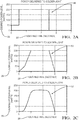
- Figs. 2A-2C arc plots illustrating examples of the dcsircd-powcr-lcvcl 26 applied to the solder-joint for the desired-time 28.
- the one or more controller-circuits 22 determine the signal 24 applied to the SCR 32 required to melt the solder-joint based on the desired-power-level 26 and the desired-time 28, thereby melting the solder-joint disposed between the pair of output-leads 46. It will be appreciated that the total energy applied to the solder-joint is indicated by an area beneath the curves of each plot, and in the examples illustrated in Figs. 2A-2C has units of Watt-seconds (W-s).
- W-s Watt-seconds
- the one or more controller-circuits 22 may be programmed with specific ramp-rates and/or dwell-times based on characteristics of the solder-joint including geometric dimensions, solder-alloy composition, and materials being joined by the solder.
- the one or more controller-circuits 22 controls the desired-power-level 26 independent of the desired-time 28. This is in contrast to prior art resistance soldering systems that typically require a total energy input be commanded, wherein the time to deliver the energy varies based on a quality of the electrical connection between the contacts and the solder-joint.
- the system 10 is an improvement over prior art resistance soldering systems because the system 10 adds another degree of freedom to the resistance soldering process, i.e., the desired-time 28.
- the one or more controller-circuits 22 controls the desired-time 28 independent of the desired-power-level 26.
- the desired-power-level 26 is characterized by a linear-function 48 and/or a piece-wise-linear-function 50.
- the desired-power-level 26 is characterized by a polynomial-function 52. Soldering profiles containing the desired-power-level 26 and the desired-time 28 are user defined and based on the characteristics of the solder-joint as described above.
- the SCR 32 further includes a voltage-output-signal 54 and a current-output-signal 56 in electrical communication with the one or more controller-circuits 22.
- the voltage-output-signal 54 and the current-output-signal 56 are indicative of a total-power 58 delivered to the primary-side 40 of the transformer 38. That is, the voltage-output-signal 54 and the current-output-signal 56 are scaled by the one or more controller-circuits 22 to determine the total-power 58 delivered to the primary-side 40 of the transformer 38, and both are characterized by electrical currents in the range of 4mA to 20mA.
- the one or more controller-circuits 22 determine the total-power 58 delivered to the pair of output-leads 46 based on the voltage-output-signal 54 and the current-output-signal 56, and may also take into account any electrical efficiency losses through the transformer 38 and/or wiring.
- the system 10 stores the voltage-output-signal 54 and the current-output-signal 56 in the memory 30 of the one or more controller-circuits 22 for historical purposes and may be accessed by an operator.
- the system 10 also includes a visual-display 60 that is a component of a human-machine-interface (HMI - not specifically shown).
- the voltage-output-signal 54 and the current-output-signal 56 are displayed on the visual-display 60 for viewing by the operator and may be used for quality control purposes.
- Figs. 3-4 illustrate additional details of the one or more controller-circuits that are used in the system 10.
- Fig. 5 is a flow chart illustrating another embodiment of a method 100 of operating a resistance soldering system 10, hereafter referred to as the system 10.
- Step 102 RECEIVE AC, includes receiving an alternating-current 14 from a power-source with a power-input-channel 12 as described above and illustrated in Fig. 1 .
- Step 104 CONVERT AC TO DC, includes converting a portion of the alternating-current 14 to a direct-current 18 at a converter-output 20 with an AC-to-DC converter 16 (AC/DC-converter 16) in electrical communication with the power-input-channel 12 as described above and illustrated in Fig. 1 .
- AC/DC-converter 16 AC-to-DC converter 16
- Step 106 includes controlling a signal 24 indicative of a desired-power-level 26 delivered for a desired-time 28 with one or more controller-circuits 22 in electrical communication with the converter-output 20.
- the signal 24 is a current-signal in a range of 0mA to 20mA, and in another embodiment (not shown), the signal 24 is a voltage-signal.
- the one or more controller-circuits 22 controls the desired-power-level 26 independent of the desired-time 28, and controls the desired-time 28 independent of the desired-power-level 26.
- Step 108 CONTROL SCR-OUTPUT-VOLTAGE, includes controlling an SCR-output-voltage 34 to a SCR-output-channel 36 proportional to the signal 24 with a silicon-controlled-rectifier 32 (SCR 32) as described above.
- the SCR-output-voltage 34 is 0VAC to 120VAC.
- the SCR 32 further includes a voltage-output-signal 54 and a current-output-signal 56 that are indicative of a total-power 58 delivered to a primary-side 40 of a transformer 38, as described above and illustrated in Fig. 1 .
- Step 110 REDUCE SCR-OUTPUT-VOLTAGE, includes reducing, with the transformer 38 the SCR-output-voltage 34 from the primary-side 40 to a secondary-voltage 44 on a secondary-side 42 of the transformer 38 as described above.
- the transformer 38 may be any transformer 38 that reduces the SCR-output-voltage 34, and preferably reduces the SCR-output-voltage 34 to a range of 0VAC to about 5VAC as described above.
- Step 112 APPLY SECONDARY-VOLTAGE, includes applying, with a pair of output-leads 46 in electrical communication with poles of the secondary-side 42 of the transformer 38, the secondary-voltage 44 to a solder-joint disposed between the pair of output-leads 46.
- the pair of output-leads 46 may terminate at corresponding electrodes that contact the solder-joint and are preferably formed of a carbon-based material, such as graphite.
- Step 114, DETERMINE SIGNAL includes determining, with the one or more controller-circuits 22, the signal 24 applied to the SCR 32 required to melt the solder-joint based on the desired-power-level 26 and the desired-time 28.
- Figs. 2A-2B illustrate the desired-power-level 26 characterized by a linear-function 48 and/or a piece-wise-linear-function 50.
- the desired-power-level 26 is characterized by a polynomial-function 52.
- the voltage-output-signal 54 and the current-output-signal 56 that are indicative of the total-power 58 delivered to the primary-side 40 of the transformer 38 are stored in a memory 30 of the one or more controller-circuits 22 as described above.
- the voltage-output-signal 54 and the current-output-signal 56 are displayed on a visual-display 60 for viewing by an operator and may be used for quality control purposes, as described above.
- Step 116 MELT SOLDER-JOINT, includes melting the solder-joint disposed between the pair of output-leads 46 with the secondary-voltage 44 as described above.
- a resistance soldering system 10 (the system 10) and a method 100 of operating the system 10 are provided.
- the system 10 is an improvement over prior art resistance soldering systems because the system 10 controls the desired-power-level 26 independent of the desired-time 28.
- first contact could be termed a second contact
- second contact could be termed a first contact
- the first contact and the second contact are both contacts, but they are not the same contact.
- the terminology used in the description of the various described embodiments herein is for the purpose of describing particular embodiments only and is not intended to be limiting. As used in the description of the various described embodiments and the appended claims, the singular forms "a”, “an” and “the” are intended to include the plural forms as well, unless the context clearly indicates otherwise. It will also be understood that the term “and/or” as used herein refers to and encompasses any and all possible combinations of one or more of the associated listed items.
- the phrase “if it is determined” or “if [a stated condition or event] is detected” is, optionally, construed to mean “upon determining” or “in response to determining” or “upon detecting [the stated condition or event]” or “in response to detecting [the stated condition or event],” depending on the context.
Landscapes
- Engineering & Computer Science (AREA)
- Mechanical Engineering (AREA)
- Physics & Mathematics (AREA)
- General Physics & Mathematics (AREA)
- Automation & Control Theory (AREA)
- Rectifiers (AREA)
- Dc-Dc Converters (AREA)
- Electric Connection Of Electric Components To Printed Circuits (AREA)
- Arc Welding Control (AREA)
- Generation Of Surge Voltage And Current (AREA)
- Control Of Voltage And Current In General (AREA)
Claims (15)
- Widerstandslötsystem (10), wobei das System (10) umfasst:einen Leistungsaufnahmekanal (12), wobei der Leistungsaufnahmekanal (12) einen Wechselstrom (14) von einer Energiequelle empfängt;einen ac-dc-Wandler (16), der mit dem Leistungsaufnahmekanal (12) elektrisch verbunden ist, wobei der ac-dc-Wandler (16) einen Teil des Wechselstroms (14) in einen Gleichstrom (18) an einem Wandlerausgang (20) umwandelt;eine oder mehrere Steuerschaltungen (22), welche mit dem Wandlerausgang (20) elektrisch verbunden sind, wobei die eine oder die mehreren Steuerschaltungen (22) ein Signal (24) steuern, das eine gewünschte Leistungsstufe (26), die für eine gewünschte Zeit (28) zur Verfügung gestellt wird, anzeigt;wobei das System gekennzeichnet ist durch:einen gesteuerten Silizium-Gleichrichter (SCR, 32), der mit dem Leistungsaufnahmekanal (12), dem Wandlerausgang (20) und dem Signal (24) elektrisch verbunden ist, wobei der gesteuerte Silizium-Gleichrichter (32) eine SCR-Ausgangsspannung (34) an einem SCR-Ausgangskanal (36) steuert, welche proportional zu dem Signal (24) ist; undeinen Transformator (38), der eine Primärseite (40) und eine Sekundärseite (42) aufweist, wobei die Primärseite (40) mit dem SCR-Ausgangskanal (36) elektrisch verbunden ist, wobei der Transformator (38) die SCR-Ausgangsspannung (34) von der Primärseite (40) auf eine Sekundärspannung (44) an der Sekundärseite (42) reduziert; undein Paar von Ausgangsleitungen (46), die mit Polen der Sekundärseite (42) des Transformators (38) elektrisch verbunden sind, wobei das Paar von Ausgangsleitungen (46) dazu ausgebildet ist, eine Sekundärspannung (44) an einer Lötstelle, welche zwischen dem Paar von Ausgangsleitungen (44) angeordnet ist, anzulegen;wobei die eine oder die mehreren Steuerschaltungen (22) das an dem gesteuerten Silizium-Gleichrichter (32) angelegte Signal (24), welches erforderlich ist, um die Lötstelle zu schmelzen, basierend auf der gewünschten Ausgangsleistung (26) und der gewünschten Zeit (28) bestimmen, wodurch die zwischen dem Paar von Ausgangsleitungen (46) angeordnete Lötstelle geschmolzen wird.
- Das System (10) gemäß Anspruch 1, wobei der gesteuerte Silizium-Gleichrichter (32) weiter ein Spannungsausgangssignal (54) und ein Stromausgangssignal (56), die mit dem einen oder den mehreren Steuerschaltungen (22) elektrisch verbunden sind, wobei das Spannungsausgangssignal (54) und das Stromausgangssignal (56) eine Gesamtleistung (58) anzeigen, welche der Primärseite (40) des Transformators (38) zugeführt wird, wodurch die eine oder die mehreren Steuerschaltungen (22) die Gesamtleistung (58), welche dem Paar von Ausgangsleitungen (46) zugeführt wird, basierend auf dem Spannungsausgangssignal (54) und dem Stromausgangssignal (56) bestimmen.
- Das System (10) gemäß Anspruch 2, wobei das Spannungsausgangssignal (54) und das Stromausgangssignal (56) in einem Speicher (30) der einen oder mehreren Steuerschaltungen (22) gespeichert sind.
- Das System (10) gemäß Anspruch 2, wobei das System (10) weiter eine optische Anzeige (60) umfasst, und das Spannungsausgangssignal (54) und das Stromausgangssignal (56) auf der optischen Anzeige (60) angezeigt werden.
- Das System (10) gemäß einem der vorherigen Ansprüche, wobei die eine oder die mehreren Steuerschaltungen (22) die gewünschte Leistungsstufe (26) unabhängig von der gewünschten Zeit (28) steuern.
- Das System (10) gemäß einem der vorherigen Ansprüche, wobei die eine oder die mehreren Steuerschaltungen (22) die gewünschte Zeit (28) unabhängig von der gewünschten Leistungsstufe (26) steuern.
- Das System (10) gemäß einem der vorherigen Ansprüche, wobei die gewünschte Leistungsstufe (26) durch eine Linearfunktion (48) oder durch eine Polynomfunktion (52) gekennzeichnet ist.
- Das System (10) gemäß Anspruch 7, wobei die Linearfunktion (48) durch eine abschnittsweise lineare Funktion (50) gekennzeichnet ist.
- Verfahren (100) zum Betreiben eines Widerstandslötsystems (10), wobei das Verfahren (100) folgende Schritte umfasst:Empfangen (102) eines Wechselstroms (14) von einer Energiequelle mit einem Leistungsaufnahmekanal (12);Umwandeln (104) eines Teils des Wechselstroms (14) in einen Gleichstrom (18) an einem Wandlerausgang (20) mit einem ac-dc-Wandler (16), der mit dem Leistungsaufnahmekanal (12) elektrisch verbunden ist;Steuern (106) eines Signals (24), das eine gewünschte Leistungsstufe (26), die für eine gewünschte Zeit (28) zugeführt wird, anzeigt, mit einer oder mehreren Steuerschaltungen (22), welche mit dem Wandlerausgang (20) elektrisch verbunden sind,wobei das Verfahren gekennzeichnet ist durch die Schritte:Steuern (108) einer Ausgangsspannung (34) eines gesteuerten Silizium-Gleichrichters (SCR, 32) an einem SCR-Ausgangskanal (36), welche proportional zu dem Signal (24) ist, mit einem SCR (32), der mit dem Leistungsaufnahmekanal (12), dem Wandlerausgang (20) und dem Signal (24) elektrisch verbunden ist; undReduzieren (110), mit einem Transformator (38), der eine Primärseite (40) und eine Sekundärseite (42) aufweist, der SCR-Ausgangsspannung (34) von der Primärseite (40) auf eine Sekundärspannung (44) an der Sekundärseite (42), wobei die Primärseite (40) mit dem SCR-Ausgangskanal (36) elektrisch verbunden ist; undAnlegen (112), mit einem Paar von Ausgangsleitungen (46), die mit Polen der Sekundärseite (42) des Transformators (38) elektrisch verbunden sind, einer Sekundärspannung (44) an einer Lötstelle, welche zwischen dem Paar von Ausgangsleitungen (44) angeordnet ist;Bestimmen (114), mit der einen oder mit den mehreren Steuerschaltungen (22), des an dem gesteuerten Silizium-Gleichrichter (32) angelegten Signals (24), welches erforderlich ist, um die Lötstelle zu schmelzen, basierend auf der gewünschten Ausgangsleistung (26) und der gewünschten Zeit (28), wodurch die zwischen dem Paar von Ausgangsleitungen (46) angeordnete Lötstelle geschmolzen wird (116).
- Das Verfahren (100) gemäß Anspruch 9, wobei der gesteuerte Silizium-Gleichrichter (32) weiter ein Spannungsausgangssignal (54) und ein Stromausgangssignal (56) umfasst, die mit dem einen oder den mehreren Steuerschaltungen (22) elektrisch verbunden ist, wobei das Spannungsausgangssignal (54) und das Stromausgangssignal (56) eine Gesamtleistung (58) anzeigen, welche der Primärseite (40) des Transformators (38) zugeführt wird, wobei das Verfahren weiter umfasst: das Bestimmen, mit der einen oder mit den mehreren Steuerschaltungen (22), der Gesamtleistung (58), welche dem Paar von Ausgangsleitungen (46) zugeführt wird, basierend auf dem Spannungsausgangssignal (54) und dem Stromausgangssignal (56).
- Das Verfahren (100) gemäß Anspruch 10, welches weiter umfasst: das Speichern des Spannungsausgangssignals (54) und des Stromausgangssignals (56) in einem Speicher (30) der einen oder mehreren Steuerschaltungen (22).
- Das Verfahren (100) gemäß Anspruch 10, wobei das System (10) weiter eine optische Anzeige (60) umfasst, wobei das Verfahren weiter umfasst: das Anzeigen des Spannungsausgangssignals (54) und des Stromausgangssignals (56) auf der optischen Anzeige (60).
- Das Verfahren (100) gemäß einem der Ansprüche 9 bis 12, wobei die eine oder die mehreren Steuerschaltungen (22) die gewünschte Leistungsstufe (26) unabhängig von der gewünschten Zeit (28) steuern.
- Das Verfahren (100) gemäß einem der Ansprüche 9 bis 13, wobei die eine oder die mehreren Steuerschaltungen (22) die gewünschte Zeit (28) unabhängig von der gewünschten Leistungsstufe (26) steuern.
- Das Verfahren (100) gemäß einem der Ansprüche 9 bis 14, wobei die gewünschte Leistungsstufe (26) durch eine Linearfunktion (48) oder durch eine Polynomfunktion (52) gekennzeichnet ist.
Priority Applications (1)
| Application Number | Priority Date | Filing Date | Title |
|---|---|---|---|
| EP21165445.4A EP3878588B1 (de) | 2018-06-20 | 2019-06-17 | Widerstandslötsystem und verfahren zum betrieb eines widerstandslötsystems |
Applications Claiming Priority (1)
| Application Number | Priority Date | Filing Date | Title |
|---|---|---|---|
| US16/012,919 US10926346B2 (en) | 2018-06-20 | 2018-06-20 | Resistance soldering system |
Related Child Applications (2)
| Application Number | Title | Priority Date | Filing Date |
|---|---|---|---|
| EP21165445.4A Division EP3878588B1 (de) | 2018-06-20 | 2019-06-17 | Widerstandslötsystem und verfahren zum betrieb eines widerstandslötsystems |
| EP21165445.4A Division-Into EP3878588B1 (de) | 2018-06-20 | 2019-06-17 | Widerstandslötsystem und verfahren zum betrieb eines widerstandslötsystems |
Publications (2)
| Publication Number | Publication Date |
|---|---|
| EP3620252A1 EP3620252A1 (de) | 2020-03-11 |
| EP3620252B1 true EP3620252B1 (de) | 2021-08-04 |
Family
ID=66912696
Family Applications (2)
| Application Number | Title | Priority Date | Filing Date |
|---|---|---|---|
| EP19180542.3A Active EP3620252B1 (de) | 2018-06-20 | 2019-06-17 | Widerstandslötsystem und -verfahren |
| EP21165445.4A Active EP3878588B1 (de) | 2018-06-20 | 2019-06-17 | Widerstandslötsystem und verfahren zum betrieb eines widerstandslötsystems |
Family Applications After (1)
| Application Number | Title | Priority Date | Filing Date |
|---|---|---|---|
| EP21165445.4A Active EP3878588B1 (de) | 2018-06-20 | 2019-06-17 | Widerstandslötsystem und verfahren zum betrieb eines widerstandslötsystems |
Country Status (5)
| Country | Link |
|---|---|
| US (2) | US10926346B2 (de) |
| EP (2) | EP3620252B1 (de) |
| JP (1) | JP2020032460A (de) |
| KR (1) | KR102229816B1 (de) |
| CN (2) | CN113843487B (de) |
Family Cites Families (34)
| Publication number | Priority date | Publication date | Assignee | Title |
|---|---|---|---|---|
| CA783737A (en) | 1968-04-23 | A. Burton Charles | Resistance soldering apparatus | |
| US2790059A (en) | 1955-06-13 | 1957-04-23 | Zepher Mfg Co | Resistance soldering device and method |
| US2969449A (en) | 1959-08-25 | 1961-01-24 | Jonathan E Tyler | Resistance soldering power supply |
| US3379896A (en) | 1964-09-03 | 1968-04-23 | Electro Miniatures Corp | Automatic resistance soldering apparatus and the like |
| US3366920A (en) | 1965-11-22 | 1968-01-30 | Amp Inc | Coaxial connector |
| US3605236A (en) | 1968-12-11 | 1971-09-20 | Burndy Corp | Assembling and positioning device for coaxial electrical contacts |
| US3621193A (en) | 1970-09-21 | 1971-11-16 | Nasa | Positive contact resistance soldering unit |
| US3778581A (en) * | 1972-08-03 | 1973-12-11 | Hughes Aircraft Co | Time-at-temperature a-c reflow soldering power supply |
| US3962562A (en) | 1974-01-14 | 1976-06-08 | Burroughs Corporation | Resistance solder unit control |
| GB2066591B (en) | 1979-12-13 | 1983-12-21 | Bunker Ramo | Electrical connector shell and method of making same |
| US4388515A (en) * | 1981-03-19 | 1983-06-14 | Pertron Controls Corporation | Resistance welding control system |
| NL8503353A (nl) | 1985-12-05 | 1987-07-01 | Weld Equip Bv | Inrichting voor het elektronisch sturen en controleren van de temperatuur en het energieverloop van een soldeer- of laselektrode. |
| DE9204968U1 (de) | 1992-04-09 | 1992-08-27 | Siemens AG, 8000 München | Abschirmungsanordnung für Durchbrüche in Gehäusewänden von HF-dichten Gehäusen |
| EP0688626B1 (de) * | 1994-05-27 | 2000-02-16 | Kabushiki Kaisha Toshiba | Steueranlage für Widerstandsschweissmaschine |
| JP2919816B2 (ja) | 1997-08-05 | 1999-07-19 | 日本アビオニクス株式会社 | パルスヒート式接合装置およびその制御方法 |
| US6013892A (en) * | 1998-01-27 | 2000-01-11 | Square D Company | Resistance weld control with line impedance compensation |
| US6326580B1 (en) * | 1999-08-23 | 2001-12-04 | Miyachi Technos Corporation | Joining apparatus |
| JP4426693B2 (ja) * | 2000-03-22 | 2010-03-03 | ミヤチテクノス株式会社 | 金属部材接合方法及びリフローハンダ付方法 |
| WO2002007312A2 (en) * | 2000-07-13 | 2002-01-24 | Isothermal Systems Research, Inc. | Power semiconductor switching devices, power converters, integrated circuit assemblies, integrated circuitry, power current switching methods, methods of forming a power semiconductor switching device, power conversion methods, power semiconductor switching device packaging methods, and methods of forming a power transistor |
| FR2821682B1 (fr) * | 2001-03-01 | 2003-05-30 | Usinor | Procede de controle et de commande d'un processus technique |
| JP2003071560A (ja) | 2001-08-30 | 2003-03-11 | Mitsubishi Heavy Ind Ltd | タービン翼のステライト鑞付装置 |
| KR100907651B1 (ko) * | 2002-12-23 | 2009-07-14 | 주식회사 포스코 | 저항 용접기용 정전력 제어장치 및 방법 |
| US7727018B2 (en) | 2008-04-22 | 2010-06-01 | Tyco Electronics Corporation | EMI gasket for an electrical connector assembly |
| WO2010030622A1 (en) | 2008-09-09 | 2010-03-18 | Molex Incorporated | Connector with impedance tuned terminal arrangement |
| US8147272B2 (en) | 2010-02-04 | 2012-04-03 | Tyco Electronics Corporation | Header connector assembly |
| US9035626B2 (en) * | 2010-08-18 | 2015-05-19 | Volterra Semiconductor Corporation | Switching circuits for extracting power from an electric power source and associated methods |
| CN202741914U (zh) * | 2012-06-25 | 2013-02-20 | 应城骏腾发自动焊接装备有限公司 | 中频逆变直流焊接电源 |
| CN103008865B (zh) * | 2012-12-31 | 2015-02-04 | 天津商科数控设备有限公司 | 脉宽可调式交直流逆变电阻焊接的工艺方法 |
| EP2843774B1 (de) | 2013-08-26 | 2016-05-25 | Delphi Technologies, Inc. | Elektromagnetische Abschirmungsbaugruppe für eine elektrische Verbinderanordnung hoher Leistung |
| US20160175968A1 (en) * | 2014-12-19 | 2016-06-23 | Illinois Tool Works Inc. | Method and apparatus for providing welding and auxiliary power |
| US9808881B2 (en) * | 2015-03-03 | 2017-11-07 | Illinois Tool Works Inc. | Method and apparatus for providing welding and auxiliary power |
| US9413115B1 (en) | 2015-05-14 | 2016-08-09 | Tyco Electronics Corporation | EMI gasket for electrical connector assembly |
| EP3107155B8 (de) | 2015-06-16 | 2019-01-16 | Aptiv Technologies Limited | Elektrisches steckverbindersystem mit abschirmungshülse und verfahren dafür |
| EP3220483A1 (de) | 2016-03-17 | 2017-09-20 | TE Connectivity Germany GmbH | Elektrische verbindungsvorrichtung, verfahren zur montage eines elektrischen kabels und montiertes elektrisches koaxialkabel |
-
2018
- 2018-06-20 US US16/012,919 patent/US10926346B2/en active Active
-
2019
- 2019-06-17 EP EP19180542.3A patent/EP3620252B1/de active Active
- 2019-06-17 KR KR1020190071644A patent/KR102229816B1/ko active Active
- 2019-06-17 EP EP21165445.4A patent/EP3878588B1/de active Active
- 2019-06-19 CN CN202111115027.1A patent/CN113843487B/zh active Active
- 2019-06-19 CN CN201910531588.6A patent/CN110614419B/zh active Active
- 2019-06-19 JP JP2019113299A patent/JP2020032460A/ja active Pending
-
2021
- 2021-01-14 US US17/148,925 patent/US11819951B2/en active Active
Also Published As
| Publication number | Publication date |
|---|---|
| CN113843487B (zh) | 2023-03-17 |
| KR102229816B1 (ko) | 2021-03-22 |
| US11819951B2 (en) | 2023-11-21 |
| EP3878588A1 (de) | 2021-09-15 |
| US10926346B2 (en) | 2021-02-23 |
| EP3878588B1 (de) | 2023-05-10 |
| CN110614419B (zh) | 2021-10-08 |
| CN110614419A (zh) | 2019-12-27 |
| EP3620252A1 (de) | 2020-03-11 |
| KR20190143392A (ko) | 2019-12-30 |
| US20190388990A1 (en) | 2019-12-26 |
| CN113843487A (zh) | 2021-12-28 |
| US20210129249A1 (en) | 2021-05-06 |
| JP2020032460A (ja) | 2020-03-05 |
Similar Documents
| Publication | Publication Date | Title |
|---|---|---|
| US11766733B2 (en) | Welding system utilizing a distributed power bus | |
| US8704130B2 (en) | Auxiliary power supply for a welding machine | |
| US7675265B2 (en) | Battery charger capable of suppressing the temperature increase of the power source circuit | |
| US20100301029A1 (en) | Wire feeder with auto-configure power supply | |
| CN103732342B (zh) | 使用焊接电源总线操作非焊接设备的系统和方法 | |
| CN105980093B (zh) | 具有总线控制系统的焊接送丝机以及操作具有总线控制系统的焊接送丝机的方法 | |
| WO2012134946A1 (en) | A system with welding power supply and controlled auxiliary power; corresponding method | |
| US10926346B2 (en) | Resistance soldering system | |
| EP2306213B1 (de) | Energiesparsystem für ein Haushaltsgerät | |
| JP4878493B2 (ja) | 電池残量判定方法および装置ならびにそれを用いる電池パック | |
| CN108112239B (zh) | 具有输入电流限制的焊接的系统和方法 | |
| US8618441B2 (en) | Output control for auto-reconnect welding/cutting equipment | |
| JP2020032460A5 (de) | ||
| EP3397417B1 (de) | Konstantstromsteuerungssysteme und -verfahren | |
| KR100707868B1 (ko) | 전기 용접기 | |
| CN105813880A (zh) | 用于使电机运行的设备和方法 | |
| WO2019067362A1 (en) | AUTOMATIC RANGE CONTROL SYSTEMS AND METHODS |
Legal Events
| Date | Code | Title | Description |
|---|---|---|---|
| PUAI | Public reference made under article 153(3) epc to a published international application that has entered the european phase |
Free format text: ORIGINAL CODE: 0009012 |
|
| STAA | Information on the status of an ep patent application or granted ep patent |
Free format text: STATUS: THE APPLICATION HAS BEEN PUBLISHED |
|
| AK | Designated contracting states |
Kind code of ref document: A1 Designated state(s): AL AT BE BG CH CY CZ DE DK EE ES FI FR GB GR HR HU IE IS IT LI LT LU LV MC MK MT NL NO PL PT RO RS SE SI SK SM TR |
|
| AX | Request for extension of the european patent |
Extension state: BA ME |
|
| STAA | Information on the status of an ep patent application or granted ep patent |
Free format text: STATUS: REQUEST FOR EXAMINATION WAS MADE |
|
| 17P | Request for examination filed |
Effective date: 20200909 |
|
| RBV | Designated contracting states (corrected) |
Designated state(s): AL AT BE BG CH CY CZ DE DK EE ES FI FR GB GR HR HU IE IS IT LI LT LU LV MC MK MT NL NO PL PT RO RS SE SI SK SM TR |
|
| GRAP | Despatch of communication of intention to grant a patent |
Free format text: ORIGINAL CODE: EPIDOSNIGR1 |
|
| RIC1 | Information provided on ipc code assigned before grant |
Ipc: B23K 3/03 20060101ALI20210128BHEP Ipc: B23K 11/24 20060101ALI20210128BHEP Ipc: B23K 1/00 20060101AFI20210128BHEP |
|
| STAA | Information on the status of an ep patent application or granted ep patent |
Free format text: STATUS: GRANT OF PATENT IS INTENDED |
|
| INTG | Intention to grant announced |
Effective date: 20210304 |
|
| GRAJ | Information related to disapproval of communication of intention to grant by the applicant or resumption of examination proceedings by the epo deleted |
Free format text: ORIGINAL CODE: EPIDOSDIGR1 |
|
| STAA | Information on the status of an ep patent application or granted ep patent |
Free format text: STATUS: REQUEST FOR EXAMINATION WAS MADE |
|
| GRAS | Grant fee paid |
Free format text: ORIGINAL CODE: EPIDOSNIGR3 |
|
| STAA | Information on the status of an ep patent application or granted ep patent |
Free format text: STATUS: GRANT OF PATENT IS INTENDED |
|
| GRAP | Despatch of communication of intention to grant a patent |
Free format text: ORIGINAL CODE: EPIDOSNIGR1 |
|
| INTC | Intention to grant announced (deleted) | ||
| INTG | Intention to grant announced |
Effective date: 20210507 |
|
| GRAA | (expected) grant |
Free format text: ORIGINAL CODE: 0009210 |
|
| STAA | Information on the status of an ep patent application or granted ep patent |
Free format text: STATUS: THE PATENT HAS BEEN GRANTED |
|
| AK | Designated contracting states |
Kind code of ref document: B1 Designated state(s): AL AT BE BG CH CY CZ DE DK EE ES FI FR GB GR HR HU IE IS IT LI LT LU LV MC MK MT NL NO PL PT RO RS SE SI SK SM TR |
|
| REG | Reference to a national code |
Ref country code: GB Ref legal event code: FG4D |
|
| REG | Reference to a national code |
Ref country code: AT Ref legal event code: REF Ref document number: 1416474 Country of ref document: AT Kind code of ref document: T Effective date: 20210815 |
|
| REG | Reference to a national code |
Ref country code: CH Ref legal event code: EP |
|
| REG | Reference to a national code |
Ref country code: DE Ref legal event code: R096 Ref document number: 602019006559 Country of ref document: DE |
|
| REG | Reference to a national code |
Ref country code: IE Ref legal event code: FG4D |
|
| REG | Reference to a national code |
Ref country code: DE Ref legal event code: R081 Ref document number: 602019006559 Country of ref document: DE Owner name: APTIV TECHNOLOGIES LIMITED, BB Free format text: FORMER OWNER: ANTAYA TECHNOLOGIES CORPORATION, WARWICK, RI, US Ref country code: DE Ref legal event code: R081 Ref document number: 602019006559 Country of ref document: DE Owner name: APTIV TECHNOLOGIES AG, CH Free format text: FORMER OWNER: ANTAYA TECHNOLOGIES CORPORATION, WARWICK, RI, US |
|
| REG | Reference to a national code |
Ref country code: LT Ref legal event code: MG9D |
|
| REG | Reference to a national code |
Ref country code: NL Ref legal event code: MP Effective date: 20210804 |
|
| REG | Reference to a national code |
Ref country code: AT Ref legal event code: MK05 Ref document number: 1416474 Country of ref document: AT Kind code of ref document: T Effective date: 20210804 |
|
| PG25 | Lapsed in a contracting state [announced via postgrant information from national office to epo] |
Ref country code: HR Free format text: LAPSE BECAUSE OF FAILURE TO SUBMIT A TRANSLATION OF THE DESCRIPTION OR TO PAY THE FEE WITHIN THE PRESCRIBED TIME-LIMIT Effective date: 20210804 Ref country code: NO Free format text: LAPSE BECAUSE OF FAILURE TO SUBMIT A TRANSLATION OF THE DESCRIPTION OR TO PAY THE FEE WITHIN THE PRESCRIBED TIME-LIMIT Effective date: 20211104 Ref country code: PT Free format text: LAPSE BECAUSE OF FAILURE TO SUBMIT A TRANSLATION OF THE DESCRIPTION OR TO PAY THE FEE WITHIN THE PRESCRIBED TIME-LIMIT Effective date: 20211206 Ref country code: AT Free format text: LAPSE BECAUSE OF FAILURE TO SUBMIT A TRANSLATION OF THE DESCRIPTION OR TO PAY THE FEE WITHIN THE PRESCRIBED TIME-LIMIT Effective date: 20210804 Ref country code: BG Free format text: LAPSE BECAUSE OF FAILURE TO SUBMIT A TRANSLATION OF THE DESCRIPTION OR TO PAY THE FEE WITHIN THE PRESCRIBED TIME-LIMIT Effective date: 20211104 Ref country code: LT Free format text: LAPSE BECAUSE OF FAILURE TO SUBMIT A TRANSLATION OF THE DESCRIPTION OR TO PAY THE FEE WITHIN THE PRESCRIBED TIME-LIMIT Effective date: 20210804 Ref country code: RS Free format text: LAPSE BECAUSE OF FAILURE TO SUBMIT A TRANSLATION OF THE DESCRIPTION OR TO PAY THE FEE WITHIN THE PRESCRIBED TIME-LIMIT Effective date: 20210804 Ref country code: SE Free format text: LAPSE BECAUSE OF FAILURE TO SUBMIT A TRANSLATION OF THE DESCRIPTION OR TO PAY THE FEE WITHIN THE PRESCRIBED TIME-LIMIT Effective date: 20210804 Ref country code: FI Free format text: LAPSE BECAUSE OF FAILURE TO SUBMIT A TRANSLATION OF THE DESCRIPTION OR TO PAY THE FEE WITHIN THE PRESCRIBED TIME-LIMIT Effective date: 20210804 Ref country code: ES Free format text: LAPSE BECAUSE OF FAILURE TO SUBMIT A TRANSLATION OF THE DESCRIPTION OR TO PAY THE FEE WITHIN THE PRESCRIBED TIME-LIMIT Effective date: 20210804 |
|
| PG25 | Lapsed in a contracting state [announced via postgrant information from national office to epo] |
Ref country code: PL Free format text: LAPSE BECAUSE OF FAILURE TO SUBMIT A TRANSLATION OF THE DESCRIPTION OR TO PAY THE FEE WITHIN THE PRESCRIBED TIME-LIMIT Effective date: 20210804 Ref country code: LV Free format text: LAPSE BECAUSE OF FAILURE TO SUBMIT A TRANSLATION OF THE DESCRIPTION OR TO PAY THE FEE WITHIN THE PRESCRIBED TIME-LIMIT Effective date: 20210804 Ref country code: GR Free format text: LAPSE BECAUSE OF FAILURE TO SUBMIT A TRANSLATION OF THE DESCRIPTION OR TO PAY THE FEE WITHIN THE PRESCRIBED TIME-LIMIT Effective date: 20211105 |
|
| PG25 | Lapsed in a contracting state [announced via postgrant information from national office to epo] |
Ref country code: NL Free format text: LAPSE BECAUSE OF FAILURE TO SUBMIT A TRANSLATION OF THE DESCRIPTION OR TO PAY THE FEE WITHIN THE PRESCRIBED TIME-LIMIT Effective date: 20210804 |
|
| PG25 | Lapsed in a contracting state [announced via postgrant information from national office to epo] |
Ref country code: DK Free format text: LAPSE BECAUSE OF FAILURE TO SUBMIT A TRANSLATION OF THE DESCRIPTION OR TO PAY THE FEE WITHIN THE PRESCRIBED TIME-LIMIT Effective date: 20210804 |
|
| REG | Reference to a national code |
Ref country code: DE Ref legal event code: R097 Ref document number: 602019006559 Country of ref document: DE |
|
| PG25 | Lapsed in a contracting state [announced via postgrant information from national office to epo] |
Ref country code: SM Free format text: LAPSE BECAUSE OF FAILURE TO SUBMIT A TRANSLATION OF THE DESCRIPTION OR TO PAY THE FEE WITHIN THE PRESCRIBED TIME-LIMIT Effective date: 20210804 Ref country code: SK Free format text: LAPSE BECAUSE OF FAILURE TO SUBMIT A TRANSLATION OF THE DESCRIPTION OR TO PAY THE FEE WITHIN THE PRESCRIBED TIME-LIMIT Effective date: 20210804 Ref country code: RO Free format text: LAPSE BECAUSE OF FAILURE TO SUBMIT A TRANSLATION OF THE DESCRIPTION OR TO PAY THE FEE WITHIN THE PRESCRIBED TIME-LIMIT Effective date: 20210804 Ref country code: EE Free format text: LAPSE BECAUSE OF FAILURE TO SUBMIT A TRANSLATION OF THE DESCRIPTION OR TO PAY THE FEE WITHIN THE PRESCRIBED TIME-LIMIT Effective date: 20210804 Ref country code: CZ Free format text: LAPSE BECAUSE OF FAILURE TO SUBMIT A TRANSLATION OF THE DESCRIPTION OR TO PAY THE FEE WITHIN THE PRESCRIBED TIME-LIMIT Effective date: 20210804 Ref country code: AL Free format text: LAPSE BECAUSE OF FAILURE TO SUBMIT A TRANSLATION OF THE DESCRIPTION OR TO PAY THE FEE WITHIN THE PRESCRIBED TIME-LIMIT Effective date: 20210804 |
|
| PLBE | No opposition filed within time limit |
Free format text: ORIGINAL CODE: 0009261 |
|
| STAA | Information on the status of an ep patent application or granted ep patent |
Free format text: STATUS: NO OPPOSITION FILED WITHIN TIME LIMIT |
|
| 26N | No opposition filed |
Effective date: 20220506 |
|
| REG | Reference to a national code |
Ref country code: GB Ref legal event code: 732E Free format text: REGISTERED BETWEEN 20220630 AND 20220706 |
|
| PG25 | Lapsed in a contracting state [announced via postgrant information from national office to epo] |
Ref country code: IT Free format text: LAPSE BECAUSE OF FAILURE TO SUBMIT A TRANSLATION OF THE DESCRIPTION OR TO PAY THE FEE WITHIN THE PRESCRIBED TIME-LIMIT Effective date: 20210804 |
|
| PG25 | Lapsed in a contracting state [announced via postgrant information from national office to epo] |
Ref country code: SI Free format text: LAPSE BECAUSE OF FAILURE TO SUBMIT A TRANSLATION OF THE DESCRIPTION OR TO PAY THE FEE WITHIN THE PRESCRIBED TIME-LIMIT Effective date: 20210804 |
|
| PG25 | Lapsed in a contracting state [announced via postgrant information from national office to epo] |
Ref country code: MC Free format text: LAPSE BECAUSE OF FAILURE TO SUBMIT A TRANSLATION OF THE DESCRIPTION OR TO PAY THE FEE WITHIN THE PRESCRIBED TIME-LIMIT Effective date: 20210804 |
|
| REG | Reference to a national code |
Ref country code: CH Ref legal event code: PL |
|
| REG | Reference to a national code |
Ref country code: BE Ref legal event code: MM Effective date: 20220630 |
|
| PG25 | Lapsed in a contracting state [announced via postgrant information from national office to epo] |
Ref country code: LU Free format text: LAPSE BECAUSE OF NON-PAYMENT OF DUE FEES Effective date: 20220617 Ref country code: LI Free format text: LAPSE BECAUSE OF NON-PAYMENT OF DUE FEES Effective date: 20220630 Ref country code: IE Free format text: LAPSE BECAUSE OF NON-PAYMENT OF DUE FEES Effective date: 20220617 Ref country code: CH Free format text: LAPSE BECAUSE OF NON-PAYMENT OF DUE FEES Effective date: 20220630 |
|
| PG25 | Lapsed in a contracting state [announced via postgrant information from national office to epo] |
Ref country code: BE Free format text: LAPSE BECAUSE OF NON-PAYMENT OF DUE FEES Effective date: 20220630 |
|
| P01 | Opt-out of the competence of the unified patent court (upc) registered |
Effective date: 20230424 |
|
| PG25 | Lapsed in a contracting state [announced via postgrant information from national office to epo] |
Ref country code: MK Free format text: LAPSE BECAUSE OF FAILURE TO SUBMIT A TRANSLATION OF THE DESCRIPTION OR TO PAY THE FEE WITHIN THE PRESCRIBED TIME-LIMIT Effective date: 20210804 Ref country code: CY Free format text: LAPSE BECAUSE OF FAILURE TO SUBMIT A TRANSLATION OF THE DESCRIPTION OR TO PAY THE FEE WITHIN THE PRESCRIBED TIME-LIMIT Effective date: 20210804 |
|
| PG25 | Lapsed in a contracting state [announced via postgrant information from national office to epo] |
Ref country code: HU Free format text: LAPSE BECAUSE OF FAILURE TO SUBMIT A TRANSLATION OF THE DESCRIPTION OR TO PAY THE FEE WITHIN THE PRESCRIBED TIME-LIMIT; INVALID AB INITIO Effective date: 20190617 |
|
| PG25 | Lapsed in a contracting state [announced via postgrant information from national office to epo] |
Ref country code: TR Free format text: LAPSE BECAUSE OF FAILURE TO SUBMIT A TRANSLATION OF THE DESCRIPTION OR TO PAY THE FEE WITHIN THE PRESCRIBED TIME-LIMIT Effective date: 20210804 |
|
| PG25 | Lapsed in a contracting state [announced via postgrant information from national office to epo] |
Ref country code: MT Free format text: LAPSE BECAUSE OF FAILURE TO SUBMIT A TRANSLATION OF THE DESCRIPTION OR TO PAY THE FEE WITHIN THE PRESCRIBED TIME-LIMIT Effective date: 20210804 |
|
| REG | Reference to a national code |
Ref country code: DE Ref legal event code: R081 Ref document number: 602019006559 Country of ref document: DE Owner name: APTIV TECHNOLOGIES AG, CH Free format text: FORMER OWNER: APTIV TECHNOLOGIES LIMITED, ST. MICHAEL, BB |
|
| PGFP | Annual fee paid to national office [announced via postgrant information from national office to epo] |
Ref country code: DE Payment date: 20250519 Year of fee payment: 7 |
|
| PGFP | Annual fee paid to national office [announced via postgrant information from national office to epo] |
Ref country code: GB Payment date: 20250602 Year of fee payment: 7 |
|
| PGFP | Annual fee paid to national office [announced via postgrant information from national office to epo] |
Ref country code: FR Payment date: 20250611 Year of fee payment: 7 |