EP3618248B1 - Recycling von kapazitiver energie aus dem aktivmodus in den niederleistungsmodus - Google Patents
Recycling von kapazitiver energie aus dem aktivmodus in den niederleistungsmodus Download PDFInfo
- Publication number
- EP3618248B1 EP3618248B1 EP19191955.4A EP19191955A EP3618248B1 EP 3618248 B1 EP3618248 B1 EP 3618248B1 EP 19191955 A EP19191955 A EP 19191955A EP 3618248 B1 EP3618248 B1 EP 3618248B1
- Authority
- EP
- European Patent Office
- Prior art keywords
- voltage
- capacitor
- load
- during
- low power
- Prior art date
- Legal status (The legal status is an assumption and is not a legal conclusion. Google has not performed a legal analysis and makes no representation as to the accuracy of the status listed.)
- Active
Links
Images


Classifications
-
- G—PHYSICS
- G06—COMPUTING OR CALCULATING; COUNTING
- G06F—ELECTRIC DIGITAL DATA PROCESSING
- G06F1/00—Details not covered by groups G06F3/00 - G06F13/00 and G06F21/00
- G06F1/26—Power supply means, e.g. regulation thereof
- G06F1/32—Means for saving power
-
- G—PHYSICS
- G06—COMPUTING OR CALCULATING; COUNTING
- G06F—ELECTRIC DIGITAL DATA PROCESSING
- G06F1/00—Details not covered by groups G06F3/00 - G06F13/00 and G06F21/00
- G06F1/26—Power supply means, e.g. regulation thereof
-
- G—PHYSICS
- G06—COMPUTING OR CALCULATING; COUNTING
- G06F—ELECTRIC DIGITAL DATA PROCESSING
- G06F1/00—Details not covered by groups G06F3/00 - G06F13/00 and G06F21/00
- G06F1/26—Power supply means, e.g. regulation thereof
- G06F1/32—Means for saving power
- G06F1/3203—Power management, i.e. event-based initiation of a power-saving mode
- G06F1/3234—Power saving characterised by the action undertaken
- G06F1/3287—Power saving characterised by the action undertaken by switching off individual functional units in the computer system
-
- H—ELECTRICITY
- H02—GENERATION; CONVERSION OR DISTRIBUTION OF ELECTRIC POWER
- H02M—APPARATUS FOR CONVERSION BETWEEN AC AND AC, BETWEEN AC AND DC, OR BETWEEN DC AND DC, AND FOR USE WITH MAINS OR SIMILAR POWER SUPPLY SYSTEMS; CONVERSION OF DC OR AC INPUT POWER INTO SURGE OUTPUT POWER; CONTROL OR REGULATION THEREOF
- H02M3/00—Conversion of DC power input into DC power output
- H02M3/02—Conversion of DC power input into DC power output without intermediate conversion into AC
- H02M3/04—Conversion of DC power input into DC power output without intermediate conversion into AC by static converters
- H02M3/06—Conversion of DC power input into DC power output without intermediate conversion into AC by static converters using resistors or capacitors, e.g. potential divider
- H02M3/07—Conversion of DC power input into DC power output without intermediate conversion into AC by static converters using resistors or capacitors, e.g. potential divider using capacitors charged and discharged alternately by semiconductor devices with control electrode, e.g. charge pumps
-
- H—ELECTRICITY
- H02—GENERATION; CONVERSION OR DISTRIBUTION OF ELECTRIC POWER
- H02M—APPARATUS FOR CONVERSION BETWEEN AC AND AC, BETWEEN AC AND DC, OR BETWEEN DC AND DC, AND FOR USE WITH MAINS OR SIMILAR POWER SUPPLY SYSTEMS; CONVERSION OF DC OR AC INPUT POWER INTO SURGE OUTPUT POWER; CONTROL OR REGULATION THEREOF
- H02M3/00—Conversion of DC power input into DC power output
- H02M3/02—Conversion of DC power input into DC power output without intermediate conversion into AC
- H02M3/04—Conversion of DC power input into DC power output without intermediate conversion into AC by static converters
- H02M3/10—Conversion of DC power input into DC power output without intermediate conversion into AC by static converters using discharge tubes with control electrode or semiconductor devices with control electrode
- H02M3/125—Conversion of DC power input into DC power output without intermediate conversion into AC by static converters using discharge tubes with control electrode or semiconductor devices with control electrode using devices of a thyratron or thyristor type requiring extinguishing means
- H02M3/135—Conversion of DC power input into DC power output without intermediate conversion into AC by static converters using discharge tubes with control electrode or semiconductor devices with control electrode using devices of a thyratron or thyristor type requiring extinguishing means using semiconductor devices only
- H02M3/137—Conversion of DC power input into DC power output without intermediate conversion into AC by static converters using discharge tubes with control electrode or semiconductor devices with control electrode using devices of a thyratron or thyristor type requiring extinguishing means using semiconductor devices only with automatic control of output voltage or current, e.g. switching regulators
-
- H—ELECTRICITY
- H02—GENERATION; CONVERSION OR DISTRIBUTION OF ELECTRIC POWER
- H02M—APPARATUS FOR CONVERSION BETWEEN AC AND AC, BETWEEN AC AND DC, OR BETWEEN DC AND DC, AND FOR USE WITH MAINS OR SIMILAR POWER SUPPLY SYSTEMS; CONVERSION OF DC OR AC INPUT POWER INTO SURGE OUTPUT POWER; CONTROL OR REGULATION THEREOF
- H02M1/00—Details of apparatus for conversion
- H02M1/0003—Details of control, feedback or regulation circuits
- H02M1/0032—Control circuits allowing low power mode operation, e.g. in standby mode
-
- H—ELECTRICITY
- H02—GENERATION; CONVERSION OR DISTRIBUTION OF ELECTRIC POWER
- H02M—APPARATUS FOR CONVERSION BETWEEN AC AND AC, BETWEEN AC AND DC, OR BETWEEN DC AND DC, AND FOR USE WITH MAINS OR SIMILAR POWER SUPPLY SYSTEMS; CONVERSION OF DC OR AC INPUT POWER INTO SURGE OUTPUT POWER; CONTROL OR REGULATION THEREOF
- H02M1/00—Details of apparatus for conversion
- H02M1/0003—Details of control, feedback or regulation circuits
- H02M1/0032—Control circuits allowing low power mode operation, e.g. in standby mode
- H02M1/0035—Control circuits allowing low power mode operation, e.g. in standby mode using burst mode control
-
- H—ELECTRICITY
- H02—GENERATION; CONVERSION OR DISTRIBUTION OF ELECTRIC POWER
- H02M—APPARATUS FOR CONVERSION BETWEEN AC AND AC, BETWEEN AC AND DC, OR BETWEEN DC AND DC, AND FOR USE WITH MAINS OR SIMILAR POWER SUPPLY SYSTEMS; CONVERSION OF DC OR AC INPUT POWER INTO SURGE OUTPUT POWER; CONTROL OR REGULATION THEREOF
- H02M1/00—Details of apparatus for conversion
- H02M1/0045—Converters combining the concepts of switch-mode regulation and linear regulation, e.g. linear pre-regulator to switching converter, linear and switching converter in parallel, same converter or same transistor operating either in linear or switching mode
-
- Y—GENERAL TAGGING OF NEW TECHNOLOGICAL DEVELOPMENTS; GENERAL TAGGING OF CROSS-SECTIONAL TECHNOLOGIES SPANNING OVER SEVERAL SECTIONS OF THE IPC; TECHNICAL SUBJECTS COVERED BY FORMER USPC CROSS-REFERENCE ART COLLECTIONS [XRACs] AND DIGESTS
- Y02—TECHNOLOGIES OR APPLICATIONS FOR MITIGATION OR ADAPTATION AGAINST CLIMATE CHANGE
- Y02B—CLIMATE CHANGE MITIGATION TECHNOLOGIES RELATED TO BUILDINGS, e.g. HOUSING, HOUSE APPLIANCES OR RELATED END-USER APPLICATIONS
- Y02B70/00—Technologies for an efficient end-user side electric power management and consumption
- Y02B70/10—Technologies improving the efficiency by using switched-mode power supplies [SMPS], i.e. efficient power electronics conversion e.g. power factor correction or reduction of losses in power supplies or efficient standby modes
-
- Y—GENERAL TAGGING OF NEW TECHNOLOGICAL DEVELOPMENTS; GENERAL TAGGING OF CROSS-SECTIONAL TECHNOLOGIES SPANNING OVER SEVERAL SECTIONS OF THE IPC; TECHNICAL SUBJECTS COVERED BY FORMER USPC CROSS-REFERENCE ART COLLECTIONS [XRACs] AND DIGESTS
- Y02—TECHNOLOGIES OR APPLICATIONS FOR MITIGATION OR ADAPTATION AGAINST CLIMATE CHANGE
- Y02D—CLIMATE CHANGE MITIGATION TECHNOLOGIES IN INFORMATION AND COMMUNICATION TECHNOLOGIES [ICT], I.E. INFORMATION AND COMMUNICATION TECHNOLOGIES AIMING AT THE REDUCTION OF THEIR OWN ENERGY USE
- Y02D10/00—Energy efficient computing, e.g. low power processors, power management or thermal management
Definitions
- the present invention relates in general to electronic device energy conservation, and more specifically to recycling the capacitive energy stored during an active mode for use in a low power mode.
- Power efficiency is a primary consideration for electronic devices particularly those that have a limited energy source, such as battery-operated devices or those devices that use harvested energy, such as, for example, solar, piezoelectric, biochemical, thermal, etc.
- Many such devices have a low power mode, such as a sleep mode or the like, to reduce energy consumption during periods of inactivity.
- MCU microcontroller unit
- IoT Internet of Things
- the system may have periodic, and often predictable, active and low power modes. Even during the low power mode, energy is consumed to maintain power to certain circuitry, such as, for example, always-on (AON) circuitry and the like. Often, the energy consumed in the low power mode is substantial part of total energy of the system.
- AON always-on
- WO 2010/084444 A2 describes a disconnecting circuit for a power converter.
- EP 2302775 A1 describes a power supply arrangement for an integrated circuit core.
- a recycle control circuit senses the low power mode and delivers the stored charge to an always-on (AON) load in the system. The charge is used until depleted or for a programmable amount of time.
- the capacitance may include a physical power supply capacitor or an intrinsic capacitance in the system, such as a load receiving a regulated voltage. In this manner, the energy stored on a capacitor (or other capacitance) during the low power mode is reused by a smart power delivery circuit which ensures switching between the capacitance and the main energy source to achieve optimum energy utilization.
- FIG. 1 is a simplified block diagram of an electronic system or device 100 according to an example not falling into the scope of the independent claims.
- the electronic device 100 includes a main electronic circuit 102, an energy source 104, and an external device circuit 106 which may include one or more external devices including a capacitor CE.
- the energy source 104 develops and provides a source voltage VSRC to an input pin 103 of the electronic circuit 102, in which VSRC is further provided to a primary regulator (PREG) 110.
- PREG primary regulator
- the primary regulator 110 converts VSRC to an output voltage VOUT, which is provided via an output pin 105 to an input or terminal of the external device circuit 106.
- VOUT is ultimately used to charge the capacitor CE, which develops a capacitor voltage VCAP provided to another pin 109 of the electronic circuit 102.
- the electronic circuit 102 includes a linear regulator (LREG1) 112 that receives VCAP and that provides a regulated voltage VDD to an input of a main load 114.
- An internal or intrinsic capacitance CI of the main load 114 is shown represented as a capacitor coupled between VDD and a supply reference node, such as ground (DGND).
- the intrinsic capacitance CI is not a separate physical capacitor, but instead is included to represent the intrinsic capacitance of the system including the main load 114.
- VSRC and VCAP are also provided to respective inputs of a recycle control circuit 116, which selects an input voltage (e.g., VCAP, VSRC, etc.) and provides a selected voltage VSEL to an input of another linear regulator (LREG2) 118.
- LREG2 118 provides a regulated voltage VDDR to an input of an always-on (AON) load 120, in which VDDR remains powered during a low power mode.
- the recycle control circuit 116 may be powered by VSRC, VSEL or even VDDR (if available), since these voltages remain powered during the low power mode.
- the energy source 104 may be based on an AC power source or the like generally providing "unlimited" power.
- the electronic circuit 102 may be or may include a low power application in which the energy source 104 is limited.
- An example of a limited power source is a rechargeable or non-rechargeable battery or set of batteries or one or more battery cells or the like.
- Another example of a limited power source is a harvested energy system, such as a system based on solar, piezoelectric, biochemical, thermal, etc. Embodiments of the present invention are particularly advantageous for low power devices using a limited energy source.
- the primary regulator 110 may be any one of several different types of regulators, such as a DC-DC regulator, a low dropout (LDO) regulator, a linear regulator, etc.
- DC-DC converters for example, are often used for power delivery of low power systems to ensure higher power efficiency. A higher power efficiency converter conserves energy and thus may improve battery lifetime in a battery-operated system.
- a DC-DC converter generally converts an input DC voltage, such as VSRC, to the output DC voltage VOUT, which may have a different voltage level than VSRC.
- VOUT for example, may have a voltage level that is less than, greater than, or equal to the voltage level of VSRC.
- VSRC may vary within a predetermined voltage range, whereas it may be desired to generate a fixed supply voltage level for driving the main load 114 during an active mode.
- the primary regulator 110 is a DC-DC converter in which the external device circuit 106 includes an inductor (e.g., inductor L, FIG. 3 ) coupled to the capacitor CE.
- the primary regulator 110 is an LDO regulator in which the capacitor CE is a decoupling capacitor and in which VOUT and VCAP are essentially the same voltage.
- LREG1 112 and LREG2 118 may be linear regulators or the like.
- LREG1 112 is provided to maintain VDD at a constant desired voltage level for the main load 114 during the active mode.
- LREG2 118 is provided to maintain VDDR at a constant desired voltage level or within a desired voltage range for maintaining power to the AON load 120 during both the active and low power modes.
- LREG2 118 may be eliminated in which the AON load 120 is supplied directly from VSEL.
- the electronic circuit 102 may be implemented in a semiconductor chip or integrated circuit (IC) or the like.
- the electronic circuit 102 may be configured as a system on a chip or system on chip (SOC) or each block may be configured as separate discrete devices.
- the main load 114 itself may be configured as an SOC and may be or may otherwise include a low power microcontroller unit (MCU) or the like.
- MCU microcontroller unit
- the AON load 120 may control the state of the system for switching between the active and low power modes.
- the AON load 120 may include, for example, timers, clock circuitry, wakeup logic, reset functions, small control circuitry for controlling state machines, supervisory circuitry (for maintaining sanity and the like, such as controlling functions for transitioning between active and low power modes), housekeeping circuits (such as circuits for reducing surge currents and ensuring proper transition sequencing of operations during power-up indicating when back in active mode), etc.
- the recycle control circuit 116 enables VCAP to provide power to the AON load 120 during the low power mode.
- any charge on the capacitor CE, or any other capacitance in the system such as the intrinsic capacitance CI was not used and was thus wasted.
- the energy source 104 was used to provide power to the AON load 120 during the low power mode, which may limit the power provided by the energy source 104. It is well known, for example, that battery lifetime is often limited by the energy consumed in the lower power mode for low-duty cycle applications.
- a low-duty cycle application is one in which the system is awakened periodically for a relatively short period of time to perform a designated operation, and then placed back into the low power mode for a longer period of time.
- FIG. 2 shows a simplified timing diagram illustrating operation of the electronic device 100 when configured to perform a low-duty cycle application.
- the timing diagram plots normalized current versus time without specific units and is not necessarily drawn to scale.
- the timing diagram shows periods of high activity at times t0, t1, t2, etc., in which the current spikes to a "HIGH" level during each active period, each followed by long period of low activity in which the current drops to a "LOW" level.
- Each period of activity is represented as a relatively narrow spike of high current, meaning that the duration of activity is very short as compared to the periods of inactivity.
- each period of activity may be as little as 1% or less of the entire duration of each cycle.
- the LOW level of current during the periods of low activity is also not shown to scale, in which the actual current may be lower than that illustrated.
- each active mode period may consume energy at a greater rate as compared to the low power mode periods, the low power mode duration is substantially longer and thus consumes an appreciable amount of power. In fact, more energy may be consumed during the low power mode.
- the active periods may occur on a regular basis, such as every 1 microsecond ( ⁇ s), while having a very short duration, such as only about 0.0025 ⁇ s.
- the LOW current may be very low such as 1 microampere ( ⁇ A) or less, whereas the HIGH current may be significantly higher, such as on the order of 20 milliamperes (mA).
- the embodiment shown in FIG. 2 appears periodic or synchronous, in which the periods of activity occur on a regular basis. Asynchronous embodiments are also contemplated, in which the periods of low power may be non-uniform with variable durations.
- Other examples include low power Bluetooth low energy (BLE) or ZibBee Internet of Things (IoT) systems in which the system is periodically, and often regularly, placed into one of one or more low power modes with or without data retention.
- IoT MCU systems are typically designed in such a way that there are one or more high power consuming domains which remain active for short periods of time.
- the high power domain has high intrinsic capacitance which is charged each time they are active, e.g., the intrinsic capacitance CI.
- the high power domain may be supplied with a high efficiency DC-DC converter. Additionally, there exist low power consuming domains which remain active for longer periods and are often supplied with a linear regulator, which is less efficient as compared to a DC-DC converter.
- the primary regulator 110 charges the capacitor CE and the intrinsic capacitance CI of the circuit during the active mode.
- the capacitor CE is typically quite large, such as on the order of about 1 microfarad ( ⁇ F) or so.
- ⁇ F microfarad
- the AON load 120 remained empowered during the low power mode, which would otherwise consume a substantial level of energy from the energy source 104 in a conventional configuration. The loss of energy becomes significant over time for many applications, including the low duty-cycle applications in which the electronic device 100 spends most of its time in the low power mode.
- the recycle control circuit 116 alleviates this problem.
- the recycle control circuit 116 provides a smart connection between the capacitor CE and the energy source 104.
- the recycle control circuit 116 also provides a smart connection between the intrinsic capacitance CI and the energy source 104.
- the energy stored on the capacitances CE and CI which would otherwise be wasted, may instead be reused and delivered to the low power domain of the system, such as, for example, the AON load 120 and even a portion of the recycle control circuit 116 itself.
- the recycle control circuit 116 therefore, lowers the overall load on the energy source 104 especially during low power operation. For battery-operated configurations, the energy used in low power domain is supplied by a high efficiency path, thereby improving the overall battery lifetime.
- FIG. 3 is a schematic and block diagram of an electronic device 300 implemented according to an example to understand the invention, not falling into the scope of the independent claims.
- the electronic device 300 includes an electronic circuit 302, a battery 304 as the energy source, and an external device circuit 306 including an inductor L and the capacitor CE.
- the battery 304 develops and provides a battery voltage VBAT as the main source voltage to an input pin 303 of the electronic circuit 302, in which VBAT is further provided to DC-DC regulator 310 as the primary regulator of the electronic circuit 302.
- the DC-DC regulator 310 converts VBAT to an output voltage VOUT, which is provided via an output pin 305 of the electronic circuit 302 to one end of the inductor L, having its other end coupled to one end of the capacitor CE at a node developing the capacitor voltage VCAP.
- the other end of the capacitor CE is coupled to an internal supply reference node, such as DGND.
- DGND internal supply reference node
- AGND AGND outside the electronic circuit 302
- a GND pin or the like is internally coupled to DGND on the electronic circuit 302 and externally coupled to AGND.
- VOUT is ultimately used to charge the capacitor CE, and VCAP is provided to a linear regulator LREG1 312 via a pin 309 of the electronic circuit 302.
- the linear regulator LREG1 312 develops and provides a regulated voltage VDD to an input of a main load 314 in a similar manner previously described.
- the intrinsic capacitance CI is coupled between VDD and DGND.
- VBAT and VCAP are also provided to respect inputs of a recycle control circuit 316, which selects an input voltage (e.g., VCAP, VSRC, etc.) and provides a selected voltage VSEL to an input of another linear regulator LREG2 318.
- LREG2 318 provides a regulated voltage VDDR to an input of an AON load 320.
- the recycle control circuit 316 includes a comparator 330 and an analog multiplexer (MUX) 332, in which each may be powered by VBAT, VSEL, or even VDDR.
- the comparator 330 has a first input receiving VCAP, a second input receiving a reference voltage VREF, and an output coupled to a select (S) input of the MUX 332.
- the comparator 330 compares the voltage levels of VCAP to VREF, and based on the results of the comparison, controls the MUX 332 to select either VBAT or VCAP as the selected voltage VSEL. When the voltage level of VCAP is greater than the voltage level of VREF, then the comparator 330 controls the MUX 332 to select VCAP as VSEL.
- the comparator 330 controls the MUX 332 to select VBAT as VSEL.
- VCAP > VREF then the comparator 330 asserts its output high causing the MUX 332 to select its logic "1" input receiving VCAP as VSEL, and when VCAP ⁇ VREF, then the comparator 330 asserts its output low causing the MUX 332 to select its logic "0" input receiving VBAT as VSEL.
- the comparator 330 may be configured to also select VBAT as VSEL when VCAP and VREF are equal or very close to each other, or when VCAP ⁇ VREF.
- VREF is selected to have a voltage level that is at or slightly greater than the minimum operating voltage level of the AON load 320. In this manner, as long as VCAP > VREF, even during the active mode, VCAP is selected to provide power to the AON load 320. Since the capacitor CE is fully charged during the active mode, the voltage level of VCAP is greater than VREF and thus is selected to provide power to the AON load 320. This is advantageous since the capacitor CE is charged by the DC-DC regulator 310, which is the most efficient path for providing power in the system. When the mode is switched to the low power mode, the charge on the capacitor CE is initially sufficient to keep the voltage level of VCAP above VREF, so that the charge on the capacitor CE continues to provide power to the AON load 320.
- VCAP may also power the recycle control circuit 316 during the low power mode. If for any reason the voltage level of VCAP falls to the voltage level of VREF during the low power mode, then the comparator 330 switches and switches the MUX 332 to select VBAT to provide power to the AON load 320, so that operation remains uninterrupted.
- the DC-DC converter 310 is turned back on at the next active mode to recharge the capacitor CE causing the comparator 332 and the MUX 332 to switch back to VCAP.
- the comparator 330 may be configured upon power on or reset of the electronic circuit 302 to hold its output low in order to control the MUX 332 to select VBAT as default on startup.
- the AON load 320 may include a power-on reset (POR) circuit 334 for ensuring proper operation upon startup or reset of the electronic circuit 302.
- the POR circuit 334 may provide a reset (RST) signal to hold the output of the comparator 330 low in order to control the MUX 332 to select VBAT as default on startup. Thereafter, during the active and low power modes, the comparator 330 controls the MUX 332 based on the comparison between VCAP and VREF as previously described.
- FIG. 4 is a schematic and block diagram of an electronic device 400 implemented according to an example to understand the invention, not falling into the scope of the independent claims.
- the electronic device 400 is similar to the electronic device 300 in which similar or even identical components assume identical reference numerals.
- the electronic device 400 includes an electronic circuit 402, which includes similar components as the electronic circuit 302 except that the recycle control circuit 316 is replaced by a recycle control circuit 416.
- the recycle control circuit 416 is similar to the recycle control circuit 316, except that the comparator 330 is replaced by a timer 430.
- the AON load 320 provides a low power (LP) signal to the timer 430 to indicate when entering the low power mode.
- the timer 430 may also receive the RST signal from the POR circuit 334 in a similar manner previously described.
- LP low power
- the timer 430 holds its output low when RST is asserted (during POR) and during the active mode, causing the MUX 332 to select VBAT as VSEL providing power to the AON load 320.
- AON load 320 asserts LP when entering the low power mode, LP triggers the timer 430 to assert its output high.
- the MUX 332 selects VCAP as VSEL providing power to the AON load 320.
- the timer 430 times out and switches the MUX 332 back to select VBAT.
- adaptivity can be incorporated by observing or otherwise predicting energy consumption in low power mode, such as, for example, by task mapping and leakage sensor or temperature sensor monitoring.
- the timeout value of the timer 430 is selected to ensure that the capacitor CE has sufficient charge to provide power to the AON load 320 for a maximum period of time during the low power mode.
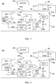
- FIG. 5 is a schematic and block diagram of an electronic device 500 implemented according to an embodiment.
- the electronic device 500 is similar to the electronic device 300 in which similar or even identical components assume identical reference numerals.
- the electronic device 500 includes an electronic circuit 502, which includes similar components as the electronic circuit 302 except that the recycle control circuit 316 is replaced by a recycle control circuit 516 and the linear regulator 318 is omitted.
- the recycle control circuit 516 is similar to the recycle control circuit 316 including the comparator 330 and the MUX 332, except that the comparator compares VREF with VDD (rather than VCAP), the logic "0" input of the MUX 332 receives VCAP instead of VBAT, and the logic "1" input of the MUX 332 receives VDD instead of VCAP.
- VBAT may provide power to the recycle control circuit 516.
- VREF is selected to have a voltage level indicative of the minimum operating voltage level of VDD.
- VDD has a high voltage level during the active mode, and discharges low via the intrinsic capacitance CI of the main load 314 during the low power mode.
- VDD is higher than VREF during the active mode so that the MUX 332 selects VDD as VSEL to provide power to the AON load 320.
- VDD is the voltage across the intrinsic capacitance CI which discharges into the AON load 320.
- the comparator 330 switches to select VCAP as VSEL to power the AON load 320 during the remaining duration of the low power mode.
- the capacitor CE may be made sufficiently large to supply power to the AON load 320 for the duration of the low power mode. Nonetheless, the charge on the intrinsic capacitance CI may be utilized during the initial portion of the low power mode.
- the linear regulator 318 is omitted, so that VSEL directly powers the AON load 320. If system boundary conditions are such that VSEL may not be used directly, then the linear regulator 318 may be included to convert VSEL to VDDR.
- the POR circuit 334 may provide RST to hold the output of the comparator 330 low in order to control the MUX 332 to select VCAP as default on startup.
- VBAT may be powered by many circuits in the AON load 320 , such as a battery voltage monitor, bandgap circuits, etc. Also, VBAT may be provided as a failsafe option in the event VCAP is less than a minimum voltage level.
- FIG. 6 is a schematic and block diagram of an electronic device 600 implemented according to another embodiment.
- the electronic device 600 is similar to the electronic device 300 in which similar or even identical components assume identical reference numerals.
- the electronic device 600 includes an electronic circuit 602, which includes similar components as the electronic circuit 302 except that the recycle control circuit 316 is replaced by a recycle control circuit 616 and the linear regulator 318 is omitted.
- the recycle control circuit 616 includes a first comparator 630, a second comparator 631 and a MUX 632.
- the first comparator 630 compares VDD with a first reference voltage VREF1 for developing a first select signal S1
- the second comparator 631 compares VCAP with a second reference voltage VREF2 for developing a second select signal S0.
- VREF1 is a minimum level of VDD
- VREF2 is a minimum level needed for the AON load 320.
- S1 and S0 are provided as a 2-bit select value to a 2-bit select input S1:0 (or S1 :S0) of the MUX 632.
- the MUX 632 receives VBAT at a binary input 00, VCAP at a binary input 01, and VDD at a binary input IX, in which "X" denotes "don't care” so that VDD may be selected provided to both binary inputs 10 and 11.
- VDD is selected as VSEL at the output of the MUX 632.
- the intrinsic capacitance CI is discharged during the initial portion of the lower power mode.
- S1 switches so that VCAP is selected as VSEL while VCAP is greater than VREF2.
- the recycle control circuit 616 of the electronic circuit 602 is essentially a combination of the other recycle control circuits 316 and 516. In this case, both capacitances CI and CE may be used to provide power to the AON load 320 during a portion up to the entire duration of the low power mode.
- the embodiments described herein are particularly advantageous for systems that are dutycycled between active and low power modes where most energy is consumed in the low power modes.
- Such systems may include, for example, MCU systems based on BLE or Zigbee or the like with or without integrated DC-DC or an LDO using an external capacitor loaded during the active mode of the system.
- the various configurations reuse the energy stored on one or both external or internal capacitance during low power mode of the system.
- the configurations include a smart power delivery scheme which ensures switching between the charged capacitance and energy source (e.g., battery) for optimum energy utilization. This scheme may be applied to the energy stored on the external capacitor, and also on the intrinsic capacitance of the main power domain that is shut-off during the low power mode.
- the always-on portion of the system may be fully or partially supplied by the energy stored on the charged capacitance.
- a preliminary evaluation may be made to determine the amount of time that the selected capacitor provides power to the low power domain load during the low power mode.
- the duration of the low power mode is known, which is usually is for many configurations, then the above relationship may be used to determine the capacitance C of the capacitor CE sufficient to provide power for the entire low power duration.
Landscapes
- Engineering & Computer Science (AREA)
- Theoretical Computer Science (AREA)
- General Engineering & Computer Science (AREA)
- Physics & Mathematics (AREA)
- General Physics & Mathematics (AREA)
- Power Engineering (AREA)
- Computer Hardware Design (AREA)
- Computing Systems (AREA)
- Dc-Dc Converters (AREA)
Claims (10)
- Elektronische Einrichtung (100, 300, 400, 500), umfassend:eine Leistungseingabe (103, 303), die ausgelegt ist zum Empfangen einer Quellspannung (VSRC, VBAT);einen Kondensatoreingang (109, 309), der ausgelegt ist zum Empfangen einer Kondensatorspannung (VCAP) von einem Kondensator (CE);eine Primärregelschaltung (110, 310) mit einem Eingang, der ausgelegt ist zum Empfangen der Quellspannung (SCRC, VBAT) und mit einem Ausgang (105, 305), der ausgelegt ist, an den Kondensator (106) gekoppelt zu werden und zum Aufrechterhalten einer Ladung auf dem Kondensator während eines aktiven Modus und nicht zu der Ladung auf dem Kondensator während eines Niedrigleistungsmodus beiträgt;eine immer eingeschaltete Last (120, 320), die während des aktiven Modus und des Niedrigenergiemodus aktiv ist;einen Sekundärregler (312) mit einem Eingang (309), der ausgelegt ist zum Empfangen der Kondensatorspannung (VCAP), und mit einem Ausgang, der ausgelegt ist zum Bereitstellen einer Regelspannung (VDD) an einem Regelspannungsknoten, der an eine intrinsische Kapazität (CI) gekoppelt ist, die die Regelspannung (VDD) während des aktiven Modus lädt; undeine Recyclesteuerschaltung (516, 616), die während des Niedrigleistungsmodus aktiv ist, umfassend:eine Wahlschaltung (332, 632), die ausgelegt ist zum Wählen, auf Basis eines Steuersignals, zwischen der Kondensatorspannung (VCAP) und mindestens der Regelspannung (VDD) an dem Regelspannungsknoten und optional der Quellspannung (VSRC, VBAT), um Leistung an die immer eingeschaltete Last (120, 320) während des Niedrigleistungsmodus zu liefern; undeine Wahlsteuerschaltung (330, 430, 630, 631), die ausgelegt ist zum Liefern des Steuersignals, um an die immer eingeschaltete Last (120, 320) während des Niedrigleistungsmodus gelieferte Leistung zu steuern;wobei die Wahlsteuerschaltung einen ersten Vergleicher (330, 630) umfasst, der ausgelegt ist zum Vergleichen der Regelspannung (VDD) an dem Regelspannungsknoten mit einer ersten vorbestimmten Referenzspannung (VREF, VREF1) und der ausgelegt ist, um ein erstes Wahlsignal (S, S1) zu liefern, das dies anzeigt;wobei das Steuersignal das erste Wahlsignal (S, S1) umfasst.
- Elektronische Einrichtung (100, 300, 400) nach Anspruch 1, weiter umfassend:
einen immer eingeschalteten Regler (318) mit einem Eingang, der ausgelegt ist zum Empfangen einer gewählten Spannung an einem Ausgang der Wahlschaltung (332), und mit einem Ausgang, der ausgelegt ist zum Liefern einer Regelspannung (VDDR) an die immer eingeschaltete Last (320). - Elektronische Einrichtung (600) nach einem vorhergehenden Anspruch,wobei die Wahlschaltung (632) ausgelegt ist zum Wählen zwischen der Kondensatorspannung (VCAP), dem Regelspannungsknoten (VDD) und der Quellspannung (VSRC, VBAT), und ausgelegt ist zum Liefern von Leistung an die immer eingeschaltete Last während des Niedrigleistungsmodus; undwobei die Wahlsteuerschaltung weiter umfasst:einen zweiten Vergleicher (631), der ausgelegt ist zum Vergleichen der Kondensatorspannung (VCAP) mit einer zweiten vorbestimmten Referenzspannung (VREF2) und ausgelegt ist zum Liefern eines zweiten Wahlsignals (S0), das dies anzeigt;wobei das Steuersignal weiter das zweite Wahlsignal (S0) umfasst.
- Elektronische Einrichtung (100) nach einem vorhergehenden Anspruch, wobei der Primärregler (310) einen DC-DC-Regler umfasst, der den Kondensator (CE) durch eine induktive Einrichtung (L) lädt.
- Elektronische Einrichtung (500) nach einem vorhergehenden Anspruch, wobei der Primärregler (310) einen Regler mit niedrigem Abfall umfasst.
- Elektronische Einrichtung (600) nach einem vorhergehenden Anspruch, wobei die Wahlschaltung (616) einen Analogmultiplexer (632) umfasst, und wobei die Wahlsteuerschaltung einen Vergleicher (630) umfasst, der das Steuersignal an einen Wahleingang des Multiplexers liefert.
- Elektronische Einrichtung nach einem vorhergehenden Anspruch, weiter umfassend einen Kondensator (CE), der zwischen dem Kondensatoreingang (309) und dem Primärreglerausgang (305) angeordnet ist, und eine an den Leistungseingang gekoppelte Energiequelle (304) .
- Verfahren zum Recyclen von Energie von einer Kapazität (CE) während eines Niedrigleistungsmodus einer elektronischen Einrichtung (500), umfassend:Laden einer Kapazität (CE) während eines aktiven Modus; undEntladen der Kapazität (CE) in eine immer eingeschaltete Last (120), so dass die immer eingeschaltete Last während des Niedrigleistungsmodus der elektronischen Einrichtung bestromt bleibt;wobei das Laden einer Kapazität das Laden eines Kondensators (CE) umfasst, um eine Kondensatorspannung (VCAP) zu entwickeln, Entwickeln einer Regelspannung (VDD) unter Verwendung der Kondensatorspannung während des aktiven Modus, und Laden einer intrinsischen Kapazität (CI) mit der geregelten Spannung (VDD);Vergleichen eines Spannungspegels der Regelspannung (VDD) mit einer vorbestimmten Referenzspannung (VREF, VREF1); undwobei das Entladen des Kondensators in eine immer eingeschaltete Last (320) während eines Niedrigleistungsmodus das Entladen der intrinsischen Kapazität (CI) in die immer eingeschaltete Last (320) umfasst, während der Spannungspegel der Regelspannung (VDD) über der vorbestimmten Referenzspannung (VREF, VREF1) ist; undEntladen des Kondensators (CE) in die immer eingeschaltete Last, wenn der Spannungspegel der Regelspannung (VDD) unter die vorbestimmte Referenzspannung (VREF, VREF1) fällt.
- Verfahren nach Anspruch 8,
wobei das Entladen des Kondensators (CE) in eine immer eingeschaltete Last (120) während eines Niedrigleistungsmodus das Entladen der Kapazität (CE) in die immer eingeschaltete Last (120) während des Niedrigleistungsmodus bis zu einer vorbestimmten Zeitperiode umfasst. - Verfahren nach einem der Ansprüche 8 oder 9, weiter umfassend:Vergleichen eines Leistungspegels der Regelspannung (VDD) mit einer ersten vorbestimmten Referenzspannung (VREF, VREF1);Vergleichen der Kondensatorspannung (VCAP) mit einer zweiten vorbestimmten Referenzspannung (VREF2); undwobei das Entladen des Kondensators in eine immer eingeschaltete Last (320) während eines Niedrigleistungsmodus das Entladen der intrinsischen Kapazität (CI) in die immer eingeschaltete Last (320) umfasst, während der Spannungspegel der Regelspannung (VDD) über der ersten vorbestimmten Referenzspannung (VREF, VREF1) ist; undEntladen des Kondensators (CE) in die immer eingeschaltete Last (320), wenn der Spannungspegel der Regelspannung (VDD) unter die erste vorbestimmte Referenzspannung (VREF, VREF1) abfällt und während die Kondensatorspannung über der zweiten vorbestimmten Referenzspannung (VREF2) liegt.
Applications Claiming Priority (1)
| Application Number | Priority Date | Filing Date | Title |
|---|---|---|---|
| US16/118,749 US11163346B2 (en) | 2018-08-31 | 2018-08-31 | Recycling capacitance energy from active mode to low power mode |
Publications (2)
| Publication Number | Publication Date |
|---|---|
| EP3618248A1 EP3618248A1 (de) | 2020-03-04 |
| EP3618248B1 true EP3618248B1 (de) | 2021-10-20 |
Family
ID=67658994
Family Applications (1)
| Application Number | Title | Priority Date | Filing Date |
|---|---|---|---|
| EP19191955.4A Active EP3618248B1 (de) | 2018-08-31 | 2019-08-15 | Recycling von kapazitiver energie aus dem aktivmodus in den niederleistungsmodus |
Country Status (2)
| Country | Link |
|---|---|
| US (1) | US11163346B2 (de) |
| EP (1) | EP3618248B1 (de) |
Families Citing this family (5)
| Publication number | Priority date | Publication date | Assignee | Title |
|---|---|---|---|---|
| US11721992B2 (en) * | 2020-07-23 | 2023-08-08 | Motorola Solutions, Inc. | System and method for supplying power from a multi-cell battery to a single-cell power management system |
| CN114265464B (zh) * | 2022-03-02 | 2022-05-20 | 南京沁恒微电子股份有限公司 | 一种带预充电功能的低功耗电源系统及其控制方法 |
| WO2023191640A1 (en) * | 2022-04-01 | 2023-10-05 | ONiO AS | Energy recycling in an embedded system |
| GB2617195B (en) * | 2022-04-01 | 2024-05-15 | ONiO AS | Energy recycling in an embedded system |
| US11775044B1 (en) | 2022-04-01 | 2023-10-03 | ONiO AS | Energy recycling in an embedded system |
Family Cites Families (9)
| Publication number | Priority date | Publication date | Assignee | Title |
|---|---|---|---|---|
| DE10106132A1 (de) | 2001-02-10 | 2002-08-14 | Philips Corp Intellectual Pty | Aufwachschaltung für ein elektrisches Gerät |
| WO2010084444A2 (en) | 2009-01-23 | 2010-07-29 | Koninklijke Philips Electronics N.V. | Low power consumption in standby mode |
| US8030909B2 (en) * | 2009-01-27 | 2011-10-04 | Texas Instruments Incorporated | Method and apparatus for switching a synchronous DC/DC converter between a PWM mode of operation and a light-load mode of operation |
| EP2302775B1 (de) | 2009-09-28 | 2012-07-25 | Nxp B.V. | Stromversorgungsanordnung für einen integrierten Schaltkern |
| CN102035369B (zh) * | 2009-09-30 | 2014-08-20 | 意法半导体研发(深圳)有限公司 | 具有电流保护的负电荷泵 |
| CN201608557U (zh) * | 2009-11-10 | 2010-10-13 | 国基电子(上海)有限公司 | 手机供电电路 |
| US9020648B2 (en) * | 2011-04-19 | 2015-04-28 | Cooper Technologies Company | Zero power appliance control, systems and methods |
| JP6172564B2 (ja) * | 2013-05-28 | 2017-08-02 | ブラザー工業株式会社 | 小容量電源、電源システム、および画像形成装置 |
| US20160087460A1 (en) * | 2014-09-23 | 2016-03-24 | The Paper Battery Company, Inc. | Ultra-capacitor structures with multiple ultra-capacitor cells and methods thereof |
-
2018
- 2018-08-31 US US16/118,749 patent/US11163346B2/en active Active
-
2019
- 2019-08-15 EP EP19191955.4A patent/EP3618248B1/de active Active
Also Published As
| Publication number | Publication date |
|---|---|
| US20200073453A1 (en) | 2020-03-05 |
| EP3618248A1 (de) | 2020-03-04 |
| US11163346B2 (en) | 2021-11-02 |
Similar Documents
| Publication | Publication Date | Title |
|---|---|---|
| EP3618248A1 (de) | Recycling von kapazitiver energie aus dem aktivmodus in den niederleistungsmodus | |
| US10320290B2 (en) | Voltage regulator with switching and low dropout modes | |
| TWI345707B (en) | Single chip microcontroller including battery management and protection | |
| CN102841668B (zh) | 具备计时电路的便携式电子设备的电力系统 | |
| CN102474188B (zh) | 电源控制装置、电源系统和电子设备 | |
| US11295787B1 (en) | Reducing SRAM leakage using scalable switched capacitor regulators | |
| CN103117567B (zh) | 一种具有充放电及电量检测功能的芯片 | |
| EP2685619B1 (de) | Effiziente Energieverwendung in Produkten mit niedrigem Energieverbrauch | |
| US9660485B2 (en) | Methods and apparatus for electronic device power | |
| US20130271092A1 (en) | Ultra-Capacitor Based Energy Storage for Appliances | |
| US20090224741A1 (en) | Low power supply maintaining circuit | |
| CA3021301A1 (en) | Door lock electrical system and method of operation | |
| JP2019195259A (ja) | スイッチキャパシタレギュレータの省電力技術 | |
| CN101233663A (zh) | 含电池管理和保护的单芯片微控制器 | |
| US7954369B2 (en) | Tire pressure measurement system with reduced current consumption | |
| KR102661979B1 (ko) | 대기전력을 차단하는 전원 어댑터 및 그 제어방법 | |
| CN112104011B (zh) | 电源管理电路以及电源管理方法 | |
| KR102428555B1 (ko) | 전자 기기의 고속 웨이크-업을 위한 직류-직류 변환 장치 및 그 동작 방법 | |
| CN112117819B (zh) | 无电池供电方法及电路 | |
| CN116707121B (zh) | 一种电能表时钟看护方法、装置及介质 | |
| EP4102335B1 (de) | Stromversorgungsschaltung, entsprechende vorrichtung und verfahren | |
| EP4629473A1 (de) | Batteriepack | |
| CN214227881U (zh) | 供电电路及仪器仪表 | |
| CN107861599A (zh) | Mcu工作电路的供电控制装置、方法与微处理器 | |
| CN120569870A (zh) | 用于气溶胶产生装置的电力供应系统 |
Legal Events
| Date | Code | Title | Description |
|---|---|---|---|
| PUAI | Public reference made under article 153(3) epc to a published international application that has entered the european phase |
Free format text: ORIGINAL CODE: 0009012 |
|
| STAA | Information on the status of an ep patent application or granted ep patent |
Free format text: STATUS: THE APPLICATION HAS BEEN PUBLISHED |
|
| AK | Designated contracting states |
Kind code of ref document: A1 Designated state(s): AL AT BE BG CH CY CZ DE DK EE ES FI FR GB GR HR HU IE IS IT LI LT LU LV MC MK MT NL NO PL PT RO RS SE SI SK SM TR |
|
| AX | Request for extension of the european patent |
Extension state: BA ME |
|
| STAA | Information on the status of an ep patent application or granted ep patent |
Free format text: STATUS: REQUEST FOR EXAMINATION WAS MADE |
|
| 17P | Request for examination filed |
Effective date: 20200904 |
|
| RBV | Designated contracting states (corrected) |
Designated state(s): AL AT BE BG CH CY CZ DE DK EE ES FI FR GB GR HR HU IE IS IT LI LT LU LV MC MK MT NL NO PL PT RO RS SE SI SK SM TR |
|
| GRAP | Despatch of communication of intention to grant a patent |
Free format text: ORIGINAL CODE: EPIDOSNIGR1 |
|
| STAA | Information on the status of an ep patent application or granted ep patent |
Free format text: STATUS: GRANT OF PATENT IS INTENDED |
|
| INTG | Intention to grant announced |
Effective date: 20210618 |
|
| GRAS | Grant fee paid |
Free format text: ORIGINAL CODE: EPIDOSNIGR3 |
|
| GRAA | (expected) grant |
Free format text: ORIGINAL CODE: 0009210 |
|
| STAA | Information on the status of an ep patent application or granted ep patent |
Free format text: STATUS: THE PATENT HAS BEEN GRANTED |
|
| AK | Designated contracting states |
Kind code of ref document: B1 Designated state(s): AL AT BE BG CH CY CZ DE DK EE ES FI FR GB GR HR HU IE IS IT LI LT LU LV MC MK MT NL NO PL PT RO RS SE SI SK SM TR |
|
| REG | Reference to a national code |
Ref country code: GB Ref legal event code: FG4D |
|
| REG | Reference to a national code |
Ref country code: CH Ref legal event code: EP |
|
| REG | Reference to a national code |
Ref country code: IE Ref legal event code: FG4D |
|
| REG | Reference to a national code |
Ref country code: DE Ref legal event code: R096 Ref document number: 602019008494 Country of ref document: DE |
|
| REG | Reference to a national code |
Ref country code: AT Ref legal event code: REF Ref document number: 1440748 Country of ref document: AT Kind code of ref document: T Effective date: 20211115 |
|
| REG | Reference to a national code |
Ref country code: LT Ref legal event code: MG9D |
|
| REG | Reference to a national code |
Ref country code: NL Ref legal event code: MP Effective date: 20211020 |
|
| REG | Reference to a national code |
Ref country code: AT Ref legal event code: MK05 Ref document number: 1440748 Country of ref document: AT Kind code of ref document: T Effective date: 20211020 |
|
| PG25 | Lapsed in a contracting state [announced via postgrant information from national office to epo] |
Ref country code: RS Free format text: LAPSE BECAUSE OF FAILURE TO SUBMIT A TRANSLATION OF THE DESCRIPTION OR TO PAY THE FEE WITHIN THE PRESCRIBED TIME-LIMIT Effective date: 20211020 Ref country code: LT Free format text: LAPSE BECAUSE OF FAILURE TO SUBMIT A TRANSLATION OF THE DESCRIPTION OR TO PAY THE FEE WITHIN THE PRESCRIBED TIME-LIMIT Effective date: 20211020 Ref country code: FI Free format text: LAPSE BECAUSE OF FAILURE TO SUBMIT A TRANSLATION OF THE DESCRIPTION OR TO PAY THE FEE WITHIN THE PRESCRIBED TIME-LIMIT Effective date: 20211020 Ref country code: BG Free format text: LAPSE BECAUSE OF FAILURE TO SUBMIT A TRANSLATION OF THE DESCRIPTION OR TO PAY THE FEE WITHIN THE PRESCRIBED TIME-LIMIT Effective date: 20220120 Ref country code: AT Free format text: LAPSE BECAUSE OF FAILURE TO SUBMIT A TRANSLATION OF THE DESCRIPTION OR TO PAY THE FEE WITHIN THE PRESCRIBED TIME-LIMIT Effective date: 20211020 |
|
| PG25 | Lapsed in a contracting state [announced via postgrant information from national office to epo] |
Ref country code: IS Free format text: LAPSE BECAUSE OF FAILURE TO SUBMIT A TRANSLATION OF THE DESCRIPTION OR TO PAY THE FEE WITHIN THE PRESCRIBED TIME-LIMIT Effective date: 20220220 Ref country code: SE Free format text: LAPSE BECAUSE OF FAILURE TO SUBMIT A TRANSLATION OF THE DESCRIPTION OR TO PAY THE FEE WITHIN THE PRESCRIBED TIME-LIMIT Effective date: 20211020 Ref country code: PT Free format text: LAPSE BECAUSE OF FAILURE TO SUBMIT A TRANSLATION OF THE DESCRIPTION OR TO PAY THE FEE WITHIN THE PRESCRIBED TIME-LIMIT Effective date: 20220221 Ref country code: PL Free format text: LAPSE BECAUSE OF FAILURE TO SUBMIT A TRANSLATION OF THE DESCRIPTION OR TO PAY THE FEE WITHIN THE PRESCRIBED TIME-LIMIT Effective date: 20211020 Ref country code: NO Free format text: LAPSE BECAUSE OF FAILURE TO SUBMIT A TRANSLATION OF THE DESCRIPTION OR TO PAY THE FEE WITHIN THE PRESCRIBED TIME-LIMIT Effective date: 20220120 Ref country code: NL Free format text: LAPSE BECAUSE OF FAILURE TO SUBMIT A TRANSLATION OF THE DESCRIPTION OR TO PAY THE FEE WITHIN THE PRESCRIBED TIME-LIMIT Effective date: 20211020 Ref country code: LV Free format text: LAPSE BECAUSE OF FAILURE TO SUBMIT A TRANSLATION OF THE DESCRIPTION OR TO PAY THE FEE WITHIN THE PRESCRIBED TIME-LIMIT Effective date: 20211020 Ref country code: HR Free format text: LAPSE BECAUSE OF FAILURE TO SUBMIT A TRANSLATION OF THE DESCRIPTION OR TO PAY THE FEE WITHIN THE PRESCRIBED TIME-LIMIT Effective date: 20211020 Ref country code: GR Free format text: LAPSE BECAUSE OF FAILURE TO SUBMIT A TRANSLATION OF THE DESCRIPTION OR TO PAY THE FEE WITHIN THE PRESCRIBED TIME-LIMIT Effective date: 20220121 Ref country code: ES Free format text: LAPSE BECAUSE OF FAILURE TO SUBMIT A TRANSLATION OF THE DESCRIPTION OR TO PAY THE FEE WITHIN THE PRESCRIBED TIME-LIMIT Effective date: 20211020 |
|
| REG | Reference to a national code |
Ref country code: DE Ref legal event code: R097 Ref document number: 602019008494 Country of ref document: DE |
|
| PG25 | Lapsed in a contracting state [announced via postgrant information from national office to epo] |
Ref country code: SM Free format text: LAPSE BECAUSE OF FAILURE TO SUBMIT A TRANSLATION OF THE DESCRIPTION OR TO PAY THE FEE WITHIN THE PRESCRIBED TIME-LIMIT Effective date: 20211020 Ref country code: SK Free format text: LAPSE BECAUSE OF FAILURE TO SUBMIT A TRANSLATION OF THE DESCRIPTION OR TO PAY THE FEE WITHIN THE PRESCRIBED TIME-LIMIT Effective date: 20211020 Ref country code: RO Free format text: LAPSE BECAUSE OF FAILURE TO SUBMIT A TRANSLATION OF THE DESCRIPTION OR TO PAY THE FEE WITHIN THE PRESCRIBED TIME-LIMIT Effective date: 20211020 Ref country code: EE Free format text: LAPSE BECAUSE OF FAILURE TO SUBMIT A TRANSLATION OF THE DESCRIPTION OR TO PAY THE FEE WITHIN THE PRESCRIBED TIME-LIMIT Effective date: 20211020 Ref country code: DK Free format text: LAPSE BECAUSE OF FAILURE TO SUBMIT A TRANSLATION OF THE DESCRIPTION OR TO PAY THE FEE WITHIN THE PRESCRIBED TIME-LIMIT Effective date: 20211020 Ref country code: CZ Free format text: LAPSE BECAUSE OF FAILURE TO SUBMIT A TRANSLATION OF THE DESCRIPTION OR TO PAY THE FEE WITHIN THE PRESCRIBED TIME-LIMIT Effective date: 20211020 |
|
| PLBE | No opposition filed within time limit |
Free format text: ORIGINAL CODE: 0009261 |
|
| STAA | Information on the status of an ep patent application or granted ep patent |
Free format text: STATUS: NO OPPOSITION FILED WITHIN TIME LIMIT |
|
| 26N | No opposition filed |
Effective date: 20220721 |
|
| PG25 | Lapsed in a contracting state [announced via postgrant information from national office to epo] |
Ref country code: AL Free format text: LAPSE BECAUSE OF FAILURE TO SUBMIT A TRANSLATION OF THE DESCRIPTION OR TO PAY THE FEE WITHIN THE PRESCRIBED TIME-LIMIT Effective date: 20211020 |
|
| PG25 | Lapsed in a contracting state [announced via postgrant information from national office to epo] |
Ref country code: SI Free format text: LAPSE BECAUSE OF FAILURE TO SUBMIT A TRANSLATION OF THE DESCRIPTION OR TO PAY THE FEE WITHIN THE PRESCRIBED TIME-LIMIT Effective date: 20211020 |
|
| PG25 | Lapsed in a contracting state [announced via postgrant information from national office to epo] |
Ref country code: MC Free format text: LAPSE BECAUSE OF FAILURE TO SUBMIT A TRANSLATION OF THE DESCRIPTION OR TO PAY THE FEE WITHIN THE PRESCRIBED TIME-LIMIT Effective date: 20211020 |
|
| REG | Reference to a national code |
Ref country code: CH Ref legal event code: PL |
|
| PG25 | Lapsed in a contracting state [announced via postgrant information from national office to epo] |
Ref country code: LU Free format text: LAPSE BECAUSE OF NON-PAYMENT OF DUE FEES Effective date: 20220815 Ref country code: LI Free format text: LAPSE BECAUSE OF NON-PAYMENT OF DUE FEES Effective date: 20220831 Ref country code: CH Free format text: LAPSE BECAUSE OF NON-PAYMENT OF DUE FEES Effective date: 20220831 |
|
| REG | Reference to a national code |
Ref country code: BE Ref legal event code: MM Effective date: 20220831 |
|
| PG25 | Lapsed in a contracting state [announced via postgrant information from national office to epo] |
Ref country code: IT Free format text: LAPSE BECAUSE OF FAILURE TO SUBMIT A TRANSLATION OF THE DESCRIPTION OR TO PAY THE FEE WITHIN THE PRESCRIBED TIME-LIMIT Effective date: 20211020 |
|
| PG25 | Lapsed in a contracting state [announced via postgrant information from national office to epo] |
Ref country code: FR Free format text: LAPSE BECAUSE OF NON-PAYMENT OF DUE FEES Effective date: 20220831 Ref country code: IE Free format text: LAPSE BECAUSE OF NON-PAYMENT OF DUE FEES Effective date: 20220815 |
|
| P01 | Opt-out of the competence of the unified patent court (upc) registered |
Effective date: 20230725 |
|
| PG25 | Lapsed in a contracting state [announced via postgrant information from national office to epo] |
Ref country code: BE Free format text: LAPSE BECAUSE OF NON-PAYMENT OF DUE FEES Effective date: 20220831 |
|
| PG25 | Lapsed in a contracting state [announced via postgrant information from national office to epo] |
Ref country code: HU Free format text: LAPSE BECAUSE OF FAILURE TO SUBMIT A TRANSLATION OF THE DESCRIPTION OR TO PAY THE FEE WITHIN THE PRESCRIBED TIME-LIMIT; INVALID AB INITIO Effective date: 20190815 |
|
| GBPC | Gb: european patent ceased through non-payment of renewal fee |
Effective date: 20230815 |
|
| PG25 | Lapsed in a contracting state [announced via postgrant information from national office to epo] |
Ref country code: CY Free format text: LAPSE BECAUSE OF FAILURE TO SUBMIT A TRANSLATION OF THE DESCRIPTION OR TO PAY THE FEE WITHIN THE PRESCRIBED TIME-LIMIT Effective date: 20211020 |
|
| PG25 | Lapsed in a contracting state [announced via postgrant information from national office to epo] |
Ref country code: MK Free format text: LAPSE BECAUSE OF FAILURE TO SUBMIT A TRANSLATION OF THE DESCRIPTION OR TO PAY THE FEE WITHIN THE PRESCRIBED TIME-LIMIT Effective date: 20211020 |
|
| PG25 | Lapsed in a contracting state [announced via postgrant information from national office to epo] |
Ref country code: GB Free format text: LAPSE BECAUSE OF NON-PAYMENT OF DUE FEES Effective date: 20230815 |
|
| PG25 | Lapsed in a contracting state [announced via postgrant information from national office to epo] |
Ref country code: GB Free format text: LAPSE BECAUSE OF NON-PAYMENT OF DUE FEES Effective date: 20230815 |
|
| PG25 | Lapsed in a contracting state [announced via postgrant information from national office to epo] |
Ref country code: MT Free format text: LAPSE BECAUSE OF FAILURE TO SUBMIT A TRANSLATION OF THE DESCRIPTION OR TO PAY THE FEE WITHIN THE PRESCRIBED TIME-LIMIT Effective date: 20211020 |
|
| PGFP | Annual fee paid to national office [announced via postgrant information from national office to epo] |
Ref country code: DE Payment date: 20250724 Year of fee payment: 7 |
|
| PG25 | Lapsed in a contracting state [announced via postgrant information from national office to epo] |
Ref country code: TR Free format text: LAPSE BECAUSE OF FAILURE TO SUBMIT A TRANSLATION OF THE DESCRIPTION OR TO PAY THE FEE WITHIN THE PRESCRIBED TIME-LIMIT Effective date: 20211020 |