EP3611535B1 - Detection of light with a plurality of avalanche photodiode elements - Google Patents
Detection of light with a plurality of avalanche photodiode elements Download PDFInfo
- Publication number
- EP3611535B1 EP3611535B1 EP19187266.2A EP19187266A EP3611535B1 EP 3611535 B1 EP3611535 B1 EP 3611535B1 EP 19187266 A EP19187266 A EP 19187266A EP 3611535 B1 EP3611535 B1 EP 3611535B1
- Authority
- EP
- European Patent Office
- Prior art keywords
- avalanche photodiode
- avalanche
- light
- elements
- photodiode element
- Prior art date
- Legal status (The legal status is an assumption and is not a legal conclusion. Google has not performed a legal analysis and makes no representation as to the accuracy of the status listed.)
- Active
Links
- 230000023077 detection of light stimulus Effects 0.000 title 1
- 230000015556 catabolic process Effects 0.000 claims description 50
- 230000035945 sensitivity Effects 0.000 claims description 43
- 230000009977 dual effect Effects 0.000 claims description 35
- 238000000034 method Methods 0.000 claims description 8
- 230000005540 biological transmission Effects 0.000 claims description 6
- 239000011159 matrix material Substances 0.000 claims description 6
- 230000005693 optoelectronics Effects 0.000 claims description 5
- 238000012544 monitoring process Methods 0.000 claims description 4
- 238000005259 measurement Methods 0.000 description 16
- 230000004913 activation Effects 0.000 description 10
- 230000008859 change Effects 0.000 description 9
- 238000001514 detection method Methods 0.000 description 7
- 230000008901 benefit Effects 0.000 description 5
- 230000000694 effects Effects 0.000 description 5
- 230000009849 deactivation Effects 0.000 description 4
- 238000011156 evaluation Methods 0.000 description 4
- 230000003287 optical effect Effects 0.000 description 4
- 238000011084 recovery Methods 0.000 description 4
- 230000002123 temporal effect Effects 0.000 description 4
- 239000002800 charge carrier Substances 0.000 description 3
- 230000001960 triggered effect Effects 0.000 description 3
- 230000008878 coupling Effects 0.000 description 2
- 238000010168 coupling process Methods 0.000 description 2
- 238000005859 coupling reaction Methods 0.000 description 2
- 230000002950 deficient Effects 0.000 description 2
- 230000005484 gravity Effects 0.000 description 2
- 230000008569 process Effects 0.000 description 2
- 230000008929 regeneration Effects 0.000 description 2
- 238000011069 regeneration method Methods 0.000 description 2
- 230000009897 systematic effect Effects 0.000 description 2
- 238000002366 time-of-flight method Methods 0.000 description 2
- FCSSPCOFDUKHPV-UHFFFAOYSA-N 2-Propenyl propyl disulfide Chemical compound CCCSSCC=C FCSSPCOFDUKHPV-UHFFFAOYSA-N 0.000 description 1
- 238000012935 Averaging Methods 0.000 description 1
- XUIMIQQOPSSXEZ-UHFFFAOYSA-N Silicon Chemical compound [Si] XUIMIQQOPSSXEZ-UHFFFAOYSA-N 0.000 description 1
- 230000006978 adaptation Effects 0.000 description 1
- 230000001419 dependent effect Effects 0.000 description 1
- 238000013461 design Methods 0.000 description 1
- 238000011161 development Methods 0.000 description 1
- 230000018109 developmental process Effects 0.000 description 1
- 238000010586 diagram Methods 0.000 description 1
- ZINJLDJMHCUBIP-UHFFFAOYSA-N ethametsulfuron-methyl Chemical compound CCOC1=NC(NC)=NC(NC(=O)NS(=O)(=O)C=2C(=CC=CC=2)C(=O)OC)=N1 ZINJLDJMHCUBIP-UHFFFAOYSA-N 0.000 description 1
- 210000003128 head Anatomy 0.000 description 1
- 230000001788 irregular Effects 0.000 description 1
- 230000000737 periodic effect Effects 0.000 description 1
- 230000036316 preload Effects 0.000 description 1
- 210000001747 pupil Anatomy 0.000 description 1
- 230000004044 response Effects 0.000 description 1
- 230000000717 retained effect Effects 0.000 description 1
- 230000002441 reversible effect Effects 0.000 description 1
- 239000000523 sample Substances 0.000 description 1
- 239000004065 semiconductor Substances 0.000 description 1
- 238000000926 separation method Methods 0.000 description 1
- 229910052710 silicon Inorganic materials 0.000 description 1
- 239000010703 silicon Substances 0.000 description 1
- 238000007619 statistical method Methods 0.000 description 1
- 230000001629 suppression Effects 0.000 description 1
- 230000001360 synchronised effect Effects 0.000 description 1
Images


Classifications
-
- G—PHYSICS
- G01—MEASURING; TESTING
- G01S—RADIO DIRECTION-FINDING; RADIO NAVIGATION; DETERMINING DISTANCE OR VELOCITY BY USE OF RADIO WAVES; LOCATING OR PRESENCE-DETECTING BY USE OF THE REFLECTION OR RERADIATION OF RADIO WAVES; ANALOGOUS ARRANGEMENTS USING OTHER WAVES
- G01S7/00—Details of systems according to groups G01S13/00, G01S15/00, G01S17/00
- G01S7/48—Details of systems according to groups G01S13/00, G01S15/00, G01S17/00 of systems according to group G01S17/00
- G01S7/481—Constructional features, e.g. arrangements of optical elements
- G01S7/4816—Constructional features, e.g. arrangements of optical elements of receivers alone
-
- G—PHYSICS
- G01—MEASURING; TESTING
- G01S—RADIO DIRECTION-FINDING; RADIO NAVIGATION; DETERMINING DISTANCE OR VELOCITY BY USE OF RADIO WAVES; LOCATING OR PRESENCE-DETECTING BY USE OF THE REFLECTION OR RERADIATION OF RADIO WAVES; ANALOGOUS ARRANGEMENTS USING OTHER WAVES
- G01S7/00—Details of systems according to groups G01S13/00, G01S15/00, G01S17/00
- G01S7/48—Details of systems according to groups G01S13/00, G01S15/00, G01S17/00 of systems according to group G01S17/00
- G01S7/483—Details of pulse systems
- G01S7/486—Receivers
- G01S7/4861—Circuits for detection, sampling, integration or read-out
- G01S7/4863—Detector arrays, e.g. charge-transfer gates
-
- G—PHYSICS
- G01—MEASURING; TESTING
- G01J—MEASUREMENT OF INTENSITY, VELOCITY, SPECTRAL CONTENT, POLARISATION, PHASE OR PULSE CHARACTERISTICS OF INFRARED, VISIBLE OR ULTRAVIOLET LIGHT; COLORIMETRY; RADIATION PYROMETRY
- G01J1/00—Photometry, e.g. photographic exposure meter
- G01J1/42—Photometry, e.g. photographic exposure meter using electric radiation detectors
- G01J1/4228—Photometry, e.g. photographic exposure meter using electric radiation detectors arrangements with two or more detectors, e.g. for sensitivity compensation
-
- G—PHYSICS
- G01—MEASURING; TESTING
- G01J—MEASUREMENT OF INTENSITY, VELOCITY, SPECTRAL CONTENT, POLARISATION, PHASE OR PULSE CHARACTERISTICS OF INFRARED, VISIBLE OR ULTRAVIOLET LIGHT; COLORIMETRY; RADIATION PYROMETRY
- G01J1/00—Photometry, e.g. photographic exposure meter
- G01J1/42—Photometry, e.g. photographic exposure meter using electric radiation detectors
- G01J1/44—Electric circuits
-
- G—PHYSICS
- G01—MEASURING; TESTING
- G01S—RADIO DIRECTION-FINDING; RADIO NAVIGATION; DETERMINING DISTANCE OR VELOCITY BY USE OF RADIO WAVES; LOCATING OR PRESENCE-DETECTING BY USE OF THE REFLECTION OR RERADIATION OF RADIO WAVES; ANALOGOUS ARRANGEMENTS USING OTHER WAVES
- G01S17/00—Systems using the reflection or reradiation of electromagnetic waves other than radio waves, e.g. lidar systems
- G01S17/02—Systems using the reflection of electromagnetic waves other than radio waves
- G01S17/06—Systems determining position data of a target
- G01S17/08—Systems determining position data of a target for measuring distance only
- G01S17/10—Systems determining position data of a target for measuring distance only using transmission of interrupted, pulse-modulated waves
-
- G—PHYSICS
- G01—MEASURING; TESTING
- G01S—RADIO DIRECTION-FINDING; RADIO NAVIGATION; DETERMINING DISTANCE OR VELOCITY BY USE OF RADIO WAVES; LOCATING OR PRESENCE-DETECTING BY USE OF THE REFLECTION OR RERADIATION OF RADIO WAVES; ANALOGOUS ARRANGEMENTS USING OTHER WAVES
- G01S17/00—Systems using the reflection or reradiation of electromagnetic waves other than radio waves, e.g. lidar systems
- G01S17/88—Lidar systems specially adapted for specific applications
- G01S17/89—Lidar systems specially adapted for specific applications for mapping or imaging
- G01S17/894—3D imaging with simultaneous measurement of time-of-flight at a 2D array of receiver pixels, e.g. time-of-flight cameras or flash lidar
-
- G—PHYSICS
- G01—MEASURING; TESTING
- G01S—RADIO DIRECTION-FINDING; RADIO NAVIGATION; DETERMINING DISTANCE OR VELOCITY BY USE OF RADIO WAVES; LOCATING OR PRESENCE-DETECTING BY USE OF THE REFLECTION OR RERADIATION OF RADIO WAVES; ANALOGOUS ARRANGEMENTS USING OTHER WAVES
- G01S7/00—Details of systems according to groups G01S13/00, G01S15/00, G01S17/00
- G01S7/48—Details of systems according to groups G01S13/00, G01S15/00, G01S17/00 of systems according to group G01S17/00
- G01S7/481—Constructional features, e.g. arrangements of optical elements
- G01S7/4817—Constructional features, e.g. arrangements of optical elements relating to scanning
-
- G—PHYSICS
- G01—MEASURING; TESTING
- G01S—RADIO DIRECTION-FINDING; RADIO NAVIGATION; DETERMINING DISTANCE OR VELOCITY BY USE OF RADIO WAVES; LOCATING OR PRESENCE-DETECTING BY USE OF THE REFLECTION OR RERADIATION OF RADIO WAVES; ANALOGOUS ARRANGEMENTS USING OTHER WAVES
- G01S7/00—Details of systems according to groups G01S13/00, G01S15/00, G01S17/00
- G01S7/48—Details of systems according to groups G01S13/00, G01S15/00, G01S17/00 of systems according to group G01S17/00
- G01S7/483—Details of pulse systems
- G01S7/486—Receivers
- G01S7/4865—Time delay measurement, e.g. time-of-flight measurement, time of arrival measurement or determining the exact position of a peak
-
- G—PHYSICS
- G01—MEASURING; TESTING
- G01S—RADIO DIRECTION-FINDING; RADIO NAVIGATION; DETERMINING DISTANCE OR VELOCITY BY USE OF RADIO WAVES; LOCATING OR PRESENCE-DETECTING BY USE OF THE REFLECTION OR RERADIATION OF RADIO WAVES; ANALOGOUS ARRANGEMENTS USING OTHER WAVES
- G01S7/00—Details of systems according to groups G01S13/00, G01S15/00, G01S17/00
- G01S7/48—Details of systems according to groups G01S13/00, G01S15/00, G01S17/00 of systems according to group G01S17/00
- G01S7/483—Details of pulse systems
- G01S7/486—Receivers
- G01S7/487—Extracting wanted echo signals, e.g. pulse detection
-
- G—PHYSICS
- G01—MEASURING; TESTING
- G01S—RADIO DIRECTION-FINDING; RADIO NAVIGATION; DETERMINING DISTANCE OR VELOCITY BY USE OF RADIO WAVES; LOCATING OR PRESENCE-DETECTING BY USE OF THE REFLECTION OR RERADIATION OF RADIO WAVES; ANALOGOUS ARRANGEMENTS USING OTHER WAVES
- G01S7/00—Details of systems according to groups G01S13/00, G01S15/00, G01S17/00
- G01S7/48—Details of systems according to groups G01S13/00, G01S15/00, G01S17/00 of systems according to group G01S17/00
- G01S7/497—Means for monitoring or calibrating
-
- H—ELECTRICITY
- H01—ELECTRIC ELEMENTS
- H01L—SEMICONDUCTOR DEVICES NOT COVERED BY CLASS H10
- H01L31/00—Semiconductor devices sensitive to infrared radiation, light, electromagnetic radiation of shorter wavelength or corpuscular radiation and specially adapted either for the conversion of the energy of such radiation into electrical energy or for the control of electrical energy by such radiation; Processes or apparatus specially adapted for the manufacture or treatment thereof or of parts thereof; Details thereof
- H01L31/02—Details
- H01L31/02016—Circuit arrangements of general character for the devices
- H01L31/02019—Circuit arrangements of general character for the devices for devices characterised by at least one potential jump barrier or surface barrier
- H01L31/02027—Circuit arrangements of general character for the devices for devices characterised by at least one potential jump barrier or surface barrier for devices working in avalanche mode
-
- G—PHYSICS
- G01—MEASURING; TESTING
- G01J—MEASUREMENT OF INTENSITY, VELOCITY, SPECTRAL CONTENT, POLARISATION, PHASE OR PULSE CHARACTERISTICS OF INFRARED, VISIBLE OR ULTRAVIOLET LIGHT; COLORIMETRY; RADIATION PYROMETRY
- G01J1/00—Photometry, e.g. photographic exposure meter
- G01J1/42—Photometry, e.g. photographic exposure meter using electric radiation detectors
- G01J1/44—Electric circuits
- G01J2001/4406—Plural ranges in circuit, e.g. switchable ranges; Adjusting sensitivity selecting gain values
-
- G—PHYSICS
- G01—MEASURING; TESTING
- G01J—MEASUREMENT OF INTENSITY, VELOCITY, SPECTRAL CONTENT, POLARISATION, PHASE OR PULSE CHARACTERISTICS OF INFRARED, VISIBLE OR ULTRAVIOLET LIGHT; COLORIMETRY; RADIATION PYROMETRY
- G01J1/00—Photometry, e.g. photographic exposure meter
- G01J1/42—Photometry, e.g. photographic exposure meter using electric radiation detectors
- G01J1/44—Electric circuits
- G01J2001/4446—Type of detector
- G01J2001/446—Photodiode
- G01J2001/4466—Avalanche
-
- G—PHYSICS
- G01—MEASURING; TESTING
- G01J—MEASUREMENT OF INTENSITY, VELOCITY, SPECTRAL CONTENT, POLARISATION, PHASE OR PULSE CHARACTERISTICS OF INFRARED, VISIBLE OR ULTRAVIOLET LIGHT; COLORIMETRY; RADIATION PYROMETRY
- G01J1/00—Photometry, e.g. photographic exposure meter
- G01J1/42—Photometry, e.g. photographic exposure meter using electric radiation detectors
- G01J1/44—Electric circuits
- G01J2001/4446—Type of detector
- G01J2001/448—Array [CCD]
-
- G—PHYSICS
- G01—MEASURING; TESTING
- G01S—RADIO DIRECTION-FINDING; RADIO NAVIGATION; DETERMINING DISTANCE OR VELOCITY BY USE OF RADIO WAVES; LOCATING OR PRESENCE-DETECTING BY USE OF THE REFLECTION OR RERADIATION OF RADIO WAVES; ANALOGOUS ARRANGEMENTS USING OTHER WAVES
- G01S17/00—Systems using the reflection or reradiation of electromagnetic waves other than radio waves, e.g. lidar systems
- G01S17/02—Systems using the reflection of electromagnetic waves other than radio waves
- G01S17/06—Systems determining position data of a target
- G01S17/08—Systems determining position data of a target for measuring distance only
- G01S17/10—Systems determining position data of a target for measuring distance only using transmission of interrupted, pulse-modulated waves
- G01S17/18—Systems determining position data of a target for measuring distance only using transmission of interrupted, pulse-modulated waves wherein range gates are used
-
- G—PHYSICS
- G01—MEASURING; TESTING
- G01S—RADIO DIRECTION-FINDING; RADIO NAVIGATION; DETERMINING DISTANCE OR VELOCITY BY USE OF RADIO WAVES; LOCATING OR PRESENCE-DETECTING BY USE OF THE REFLECTION OR RERADIATION OF RADIO WAVES; ANALOGOUS ARRANGEMENTS USING OTHER WAVES
- G01S17/00—Systems using the reflection or reradiation of electromagnetic waves other than radio waves, e.g. lidar systems
- G01S17/02—Systems using the reflection of electromagnetic waves other than radio waves
- G01S17/06—Systems determining position data of a target
- G01S17/42—Simultaneous measurement of distance and other co-ordinates
Definitions
- the invention relates to a light receiver and a method for detecting light with a plurality of avalanche photodiode elements according to the preamble of claims 1 and 9, respectively.
- the function of a light receiver is to generate an electrical signal from incoming light.
- the detection sensitivity of simple photodiodes is not sufficient in many applications.
- an avalanche photo diode APD
- the incident light triggers a controlled avalanche breakdown (avalanche effect).
- the charge carriers generated by incident photons are multiplied, and a photocurrent is generated which is proportional to the light reception intensity, but which is significantly greater than with a simple PIN diode.
- the avalanche photodiode is biased above the breakdown voltage, so that a single charge carrier released by a single photon can trigger an avalanche, which then recruits all available charge carriers due to the high field strength.
- the avalanche photo diode like the eponymous Geiger counter, counts individual events.
- Avalanche photo diodes in Geiger mode are also known as SPADs (Single-Photon Avalanche Diode).
- Geiger APDS or SPADs are very fast, highly sensitive photodiodes based on semiconductors.
- a disadvantage of the high sensitivity is that not only a useful light photon, but also a weak interference event caused by extraneous light, optical crosstalk or dark noise can trigger the avalanche breakdown. This disturbance event then contributes to the measurement result with the same relatively strong signal as the received useful light and cannot be distinguished from it from the signal either. Then the sensitivity of the avalanche photodiode for a dead or recovery time drastically reduced from approx. 5 to 100 ns, so that it practically fails for further measurements. It is therefore common to statistically evaluate several SPADs.
- a typical silicon photomultiplier (SiPM) with SPADs has several thousand SPADs.
- Light receivers with SPADs are also suitable for time of flight measurement (TOF) for distance measurement with laser pulses.
- TOF time of flight measurement
- a TDC time-to-digital converter
- the dead-time effect described can, for example, impair the measuring ability at higher temperatures with many dark events without light reception or with a lot of external light irradiation. In any case, this should be taken into account when determining a reception time, because otherwise the measured value will be falsified, especially if the number of photons reflected back from the target object within the recovery time significantly exceeds the total number of pixels.
- the EP 2 708 914 A1 discloses a SPAD-based sensor for recording a depth map, in which a transmitted light beam deflected by a MEMS mirror scans the scene. Only those SPADs are active on which the area of the scene illuminated with the transmission beam is mapped. This serves for a spatial resolution by scanning, but in no way improves the respective distance measurement at the probed location.
- the sensitivity is dynamically adjusted via the preload.
- the sensitivity is initially set to be low and then increased in accordance with the speed of propagation of light. This increases the probability that, because of the initially lower sensitivity, avalanche photodiodes that have not yet triggered are also available in the event of an echo from a distant object. In unfavorable conditions, for example with a lot of extraneous light, this measure is not sufficient, and falsifications of the measured value due to the effects of the dead times are completely disregarded.
- the DE 10 2014 207 599 A1 discloses a photodetector with a plurality of avalanche photodiodes per image point, which are activated in turn with a time offset from one another.
- the individual active time is shorter than the regeneration time, but in total across the avalanche photodiodes of a pixel, the time periods are greater than the regeneration time, so that continuous operation is made possible.
- this requires a large number of avalanche photo diodes per pixel.
- the activation sequence is the same for all image points, so that there is no flexibility in the local distribution of the respectively active avalanche photodiodes.
- a light receiver and a method for detecting light with a plurality of avalanche photodiode elements according to claims 1 and 9, respectively. If a bias voltage (bias voltage) above the breakdown voltage is applied to the avalanche photodiode elements, they work in Geiger mode.
- the avalanche photodiode elements are combined into groups, the avalanche photodiode elements of a group being distributed in particular in a pattern over the light receiver.
- the invention is based on the basic idea of adjusting the sensitivities of the groups in a time sequence.
- a temporal distribution is added to the local distribution by means of the groups.
- This sensitivity can be predetermined by the circuit, for example by resistance values, capacitances and the like in the interconnection of the avalanche photodiodes.
- the change in sensitivity preferably includes the extreme case of activation or deactivation, in particular in the form that a change is made between the linear mode and the Geiger mode. In between there is a factor of 10 5 -10 6 in the sensitivity, which equates to an activation and deactivation.
- Two avalanche photodiodes from two different groups form an at least dual avalanche photodiode with at least one front avalanche photodiode and one rear avalanche photodiode, in which an avalanche breakdown of the front avalanche photodiode changes the sensitivity of the rear avalanche photodiode.
- the terms front and rear avalanche photodiode only serve to distinguish between concepts and are based on a preferred time sequence. In fact, both avalanche photodiodes can be constructed identically or swap roles.
- the point in time at which the rear avalanche photodiode becomes active is automatically controlled by the triggering of the front avalanche photodiode.
- the avalanche breakdown of the front avalanche photodiode ensures a changed bias voltage on the rear avalanche photodiode. Changes in both directions, i.e. raising and lowering, are conceivable, and this change can gradually adjust the sensitivity by means of an adapted overvoltage or cross the threshold of the breakdown voltage and thus effectively activate or deactivate the rear avalanche photodiode.
- the invention has the advantage that a high degree of flexibility and adaptability to measurement requirements is achieved.
- groups of avalanche photodiodes are suitably distributed over the area, and their sensitivity is adjusted in a certain time sequence. This can be optimized especially for time of flight measurements in order to efficiently and cost-effectively correct or avoid measurement errors caused by a black-and-white shift.
- the dark triggers are reduced, for example approximately by half in the case of two groups that are alternately active.
- the sequential switching of an at least dual avalanche photodiode has a number of advantages. It causes a suppression of pixel crosstalk. Defective avalanche photodiodes that trigger incorrectly can be suppressed by operating the intact avalanche photodiode with a higher overvoltage and the defective avalanche photodiode only with the breakdown voltage. An extinguishing resistance, which is responsible for extinguishing the avalanche in the event of a detection event, can be reduced and thus a higher output signal can be achieved.
- the output capacitance of the light receiver can be reduced to a quarter by connecting the front and rear avalanche photodiode in series: n cells with n capacities connected in parallel are replaced by n / 2 dual cells, each with half the capacitance. It is possible that To expand the concept of dual cells to k-fold avalanche photodiodes with a chain of k avalanche photodiodes, whereby one avalanche in each avalanche photodiode changes the sensitivity of the avalanche photodiode following in the chain. Switching between the two avalanche photodiodes can take place electrically without interference, i.e. without generating interference signals during the switching process.
- the circuit complexity for the separate control of the second avalanche photodiode is minimal and only requires a coupling resistor, for example.
- the dead or recovery time can be influenced and controlled by the choice of coupling resistance and capacities. Electrical and optical crosstalk can be reduced by reducing the number of adjacent avalanche photodiodes that are active at the same time.
- the dual avalanche photodiode is assigned an interconnection unit which, in the idle state before an avalanche breakdown, holds the front avalanche photodiode to a bias voltage above and the rear avalanche photodiode to a bias voltage below the breakdown voltage.
- a voltage divider circuit is provided in particular, which represents a very simple and inexpensive implementation option. It asymmetrically distributes a total voltage that is in the order of double the breakdown voltage.
- In the idle state only the front avalanche photodiode is supplied above the breakdown voltage and is therefore active. In the event of an avalanche breakdown, it becomes low-resistance, so that a higher voltage is now applied to the rear avalanche photodiode, which brings it above the breakdown voltage and thus into Geiger mode and thus activates it.
- the total voltage and ratio are such that the front and rear avalanche photodiodes are supplied with different overvoltages and therefore differ gradually in their sensitivity, with an avalanche breakdown changing the ratio of the sensitivities.
- the avalanche breakdown in one avalanche photodiode does not ensure activation, but, conversely, deactivation of the other avalanche photodiode, the bias of which is pushed below the breakdown voltage. Both avalanche photo diodes are active in the idle state. If the received signal is strong, a receiving avalanche photodiode suppresses a received signal from its partner.
- the voltage dividers and thus the voltages applied in each case can be provided for each dual avalanche photodiode, but also connected in parallel for a plurality of avalanche photodiodes, in particular a row or column.
- the division ratio can be fixed or adjustable by the switching elements.
- avalanche photodiode elements When the bias voltage is increased above the breakdown voltage, avalanche photodiode elements are activated and / or deactivated by lowering the bias voltage below the breakdown voltage.
- the sensitivity is not only changed gradually, but the respective avalanche photodiode element is activated and / or deactivated by changing between the linear mode (APD mode) and the Geiger mode.
- the breakdown voltage is the minimum bias voltage required for Geiger mode. Strictly speaking, however, the photon detection efficiency (PDE) and the gain are still zero at this limit value. Only when the bias voltage exceeds the breakdown voltage are incident photons converted into corresponding Geiger current impulses, with the probability of triggering increasing with the overvoltage. Thus, by means of different overvoltages, a gradual sensitivity control with different sensitivities of the groups is achieved. It is also conceivable to give the same group different overvoltages and thus sensitivities at two different points in time.
- a light transit time measuring unit is preferably provided which is designed to determine a light transit time of a light pulse from the signals of the avalanche photo diode elements.
- a reception time derived from the signals is preferably compared with an optically or electrically obtained reference time of the emission of the light pulse, for example by means of TDCs. Since a measurement event and a disturbance event cannot be distinguished in a single avalanche photo diode in Geiger mode, statistical methods are preferably used over a large number of avalanche photo diodes or repeated measurements.
- the avalanche photodiode elements preferably form a matrix arrangement, each group having at least one avalanche photodiode element in each raster element in a subdivision of the matrix arrangement into a grid of grid elements.
- a matrix arrangement of nxm avalanche photodiodes is created in a grid of a large number divided by grid elements with ixj avalanche photo diodes.
- the avalanche photodiode elements of two groups preferably form a checkerboard pattern. Different grain sizes are conceivable in which areas with k avalanche photodiodes belong to the same pattern element of the chessboard.
- the checkerboard pattern can be understood as a special case of a grid of grid elements with two groups, with the additional condition that the sequence of setting the sensitivities of the avalanche photodiodes is reversed in each adjacent grid elements.
- a delay circuit is preferably provided which, after an avalanche breakdown in the front avalanche photodiode, activates or deactivates the rear avalanche photodiode after a predeterminable delay time.
- the delay time can be determined by elements of the delay circuit, or it can be set by a control.
- the choice of the ratio of a voltage divider is one way of influencing the delay time via the voltage difference required for a crossing of the bias voltage.
- an optoelectronic sensor with at least one light receiver is provided, the sensor being designed for distance measurement and / or as a code reader and / or for data transmission.
- the distance can be determined by triangulation, as in a triangulation probe or a stereo camera.
- Other non-exclusive applications of the light receiver in an optoelectronic sensor are code reading or data transmission or combinations of these applications in one sensor.
- the sensor is particularly preferably a distance measuring sensor with a light transmitter for emitting a light signal and with a light transit time measuring unit which is designed to determine a distance of the object from a light transit time between emission of the light signal and reception of the light signal reflected by the object from the monitoring area.
- the light signal preferably has a light pulse, and the sensor measures distances using the pulse method. More complicated forms such as double pulses or even pulse codes are also conceivable. It can several light pulses are sent and received one after the other and the respective individual results are statistically evaluated together, for example in a pulse averaging process.
- the time-of-flight method can be used in a one-dimensional distance sensor, a laser scanner or an image sensor of a 3D camera based on the time-of-flight principle.
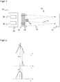
- FIG. 1 shows a schematic representation of an optoelectronic sensor 10 in an embodiment as a single-beam light scanner.
- a light transmitter 12 for example an LED or a laser light source, transmits a light signal 14 into a monitoring area 16. If it hits an object 18 there, part of the light signal is remitted or reflected and returns to a light receiver 22 as a remitted light signal 20.
- This light receiver 22 comprises a plurality of avalanche photodiode elements 24 in Geiger mode or SPADs. The received signals of the avalanche photodiode elements 24 are read out by a control and evaluation unit 26 and evaluated there.
- the control and evaluation unit 26 two blocks of the control and evaluation unit 26 are highlighted only very schematically and on a purely functional level, namely a light transit time measuring unit 28 and a control unit 30.
- the light transit time measuring unit 28 measures a light transit time from the emission of the light signal 14 to the reception of the remitted light signal 20 and converts this into a distance using the speed of light.
- the time-of-flight measuring unit 28 is not present if the sensor 10 has a task other than determining the distance using a time-of-flight method.
- the control unit 30 is able to change the sensitivity of the avalanche photodiode elements 24 in groups, as will be explained in detail further below.
- the senor 10 has further elements, in particular transmitting and receiving optics and connections, which are not discussed here for the sake of simplicity.
- the separation into light receiver 22 and control and evaluation unit 26 in Figure 1 is also conceivable in practice, but serves primarily for explanation.
- These elements are preferably at least partially integrated on a common chip, the surface of which is shared by light-sensitive areas of the avalanche photodiode elements 24 and circuits assigned to individual or groups of avalanche photodiode elements 24 for their evaluation and control.
- optical arrangement with a light transmitter 12, which covers a small portion of the light receiver 22 is purely by way of example.
- other known optical solutions can also be used, such as autocollimation with a beam splitter, for example and a common optics, or pupil division, where two separate optics are provided and the light transmitter and light receiver are arranged next to one another.
- the single-beam sensor 10 shown as a whole is also to be understood only as an example.
- An extension of the monitoring area 16 is possible by moving the beam in a laser scanner, be it with a rotating mirror or a total rotating measuring head with light transmitter 12 and / or light receiver 22.
- several single-beam systems can be combined to create a light grid with several, mostly parallel To form beams, which measures or monitors distances in each beam, in particular as a scanning light grid. It can be measured with the avalanche photodiode elements 24 individually or in groups, spatially resolved, so that a 3D camera is created.
- Mobile systems are also conceivable in which the sensor 10 is movably mounted.
- Figure 2 shows, one above the other, three representations of the time course of an accumulated received signal of the avalanche photodiode elements 24 in the region of a strong received pulse. For this purpose, the number of triggering avalanche photodiode elements 24 is plotted against time. In the upper part of the Figure 2 the entire received pulse is shown, in the middle part a remainder of the received pulse that is no longer received and in the lower part the received start area of the received pulse complementarily.
- the pulse shape is not as cleanly resolved and cut off as in the lower part of the Figure 2 so that a determination of the time of reception cannot simply be based on the maximum value that has not been shifted there. Rather, a realistic time-of-flight measurement, which for example determines the center of gravity, results in an incorrect pulse reconstruction. This leads to an error in the transit time measurement, which depends on the intensity of the received pulse and the dead time of the avalanche photodiode elements 24.
- This systematic error is a special form of the black-and-white shift or the intensity-dependent light-dark error, which has long been known for time-of-flight measurements, according to which light objects 18 are measured at a different distance than dark objects 18, now in the case of avalanche photo-diode elements 24 in Geiger mode.
- a first example according to Figure 3 two alternating groups of avalanche photo diode elements 24a-b formed, which are arranged on the light receiver 22 in a checkerboard pattern.
- the avalanche photodiode elements 24a of the first group are initially active (black) and the avalanche photodiode elements 24b of the second group are inactive (white).
- the configuration is changed with a defined time offset, now as in the right part of the Figure 3 the avalanche photodiode elements 24b of the second group are active (black) and the avalanche photodiode elements 24a of the first group are inactive (white).
- the control unit 30 can carry out this change one or more times in a regular or irregular sequence.
- the checkerboard pattern shown is just a simple example.
- the nxm avalanche photodiode elements 24 of the light receiver 22 be uniquely addressable with a pair of numbers (i, j), 1 i n, i j m.
- Now l time windows ⁇ tk, 1 k l of any length are determined, and a matrix with coefficients a k (i, j) for the sensitivity of the avalanche photo diode element 24 at position (i, j) is specified for each time window ⁇ tk.
- the coefficients a (i, j) are preferably between a minimum and maximum sensitivity and accept either only the digital values (0.1) for active and inactive or intermediate values for sensitivities in between.
- such intermediate values are preferably set by means of the value of an overvoltage above the breakdown voltage.
- the value 0 stands for below the breakdown voltage and the value 1 for a comfortable working voltage well above the breakdown voltage, the further increase of which would hardly change the sensitivity.
- the overvoltage is scaled accordingly for values between 0 and 1.
- new groups of avalanche photodiodes 24 are formed in each time window ⁇ tk, which in the extreme case each consist of only one avalanche photodiode 24.
- ⁇ tk time window
- only a few groups are preferably formed, whose group membership is retained over time, and only the sensitivity of the avalanche photodiode elements 24 of a group is changed at certain times. It is true that individual control offers the greatest flexibility, but the expense, in particular for the additional lines to each avalanche photodiode element 24, is high and reduces the fill factor. If there is a fixed group membership, however, common controls and lines can be used.
- FIG. 4 illustrates another example.
- a received pulse is shown again similar to that in FIG Figure 2 .
- the time window of the expected duration of the received pulse is subdivided, here as an example regularly and into six subsections ⁇ t1- ⁇ t6.
- a different one of six groups of avalanche photo diode elements 24 is activated, so that a population of avalanche photo diode elements 24 ready for detection is available over the entire duration of the received pulse, in which no avalanche breakdown has yet been triggered and which are not in their Dead time.
- the joint triggering with a high light load or high intensity gradients as in Figure 2 is avoided in this way.
- the electrical received pulse reconstructed from the received signal of the avalanche photodiode elements 24 does not have a shifted center of gravity; rather, its pulse shape is realistically reproduced and the black-and-white error is thus suppressed.
- Figure 5 shows a suitable possible distribution of the groups of avalanche photo diode elements 24 formed for the subsections ⁇ t1- ⁇ t6 on the light receiver 22.
- the light receiver 22 is in a regular grid of raster elements 32 divided into Figure 5 only one is exemplarily highlighted by a thick line.
- At least one avalanche photodiode element 24 of each group is provided within each raster element 32, as symbolized by numbers 1 ... 6.
- the avalanche photo diode elements 24 are thus active at number 1, and correspondingly for the further subsections ⁇ t2- ⁇ t6 the avalanche photo diode elements 24 at numbers 2 ... 6.
- the duration of the subsections ⁇ t1- ⁇ t6 is advantageously added approximately to the expected duration of the received pulse.
- the individual durations ⁇ t1- ⁇ t6 and the sequence can be uniform, but they can also be varied. A temporal overlap would also be conceivable in which at least one group is still active while the next group is already being activated.
- the control sequence is preferably repeated according to any periodic pattern in order to cover an unknown time position of the received pulse, and it can be synchronized with the transmission time of the light signal 14.
- the selected number of six subsections ⁇ t1- ⁇ t6 or six groups is only one example. However, it makes sense not to form too many groups and in particular not to form a maximum of ten groups so that a sufficient number of avalanche photodiode elements 24 is still contained in each group. Otherwise, a weaker received pulse from a distant and / or dark object 18 with too few avalanche photodiode elements 24 might no longer be detected, especially since a received light spot from the far range typically only illuminates a small part of the light receiver 22 and thus most of the avalanche photodiode elements 24 even with the highest sensitivity do not receive any useful light photons at all. A small receiving light spot from the far range can also be avoided by using homogenizing optics, such as in the DE 10 2014 102 420 A1 described, whereby as possible the entire light receiver 22 is illuminated evenly regardless of distance.
- these parameters are preferably taken into account: the photon flow, the total number of photons available avalanche photodiode elements 24, their photon detection efficiency (PDE) and their dead time.
- Figure 6 illustrates once again that not only the specifically described rasterized or checkerboard-like patterns are available for such a design, but in principle also any arrangements.
- the avalanche photodiode elements 24 active at the time under consideration are shown in black, the inactive avalanche photodiode elements 24 in white.
- such avalanche photodiode elements 24 do not have to be considered separately in that they are viewed as a further group which are set to the desired sensitivity at time zero, for example when they are switched on.
- FIG. 7 shows a basic circuit of an advantageous embodiment.
- Two avalanche photodiode elements 24a-b are connected together to form a dual avalanche photodiode 124 in such a way that the triggering of an avalanche breakdown in the one avalanche photodiode element 24a-b results in a change in sensitivity, in particular activation or deactivation, of the other avalanche photodiode element 24b- a.
- the switching elements shown are, as it were, the control unit 30 which is wholly or partially integrated into the dual avalanche photodiode 124 and which derives the point in time for a change in sensitivity dynamically from an avalanche breakdown.
- the two avalanche photodiode elements 24a-b advantageously share a charging resistor Rk.
- the two avalanche photodiode elements 24a-b are sometimes also referred to as the front avalanche photodiode element 24a and the rear avalanche photodiode element 24b. However, this is only a linguistic simplification that is based on the chronological sequence in a preferred embodiment.
- the rear avalanche photodiode element 24b can also be active first and activate the front avalanche photodiode element 24a, one avalanche photodiode element 24a-b temporarily suppressing the activity of the other avalanche photodiode element 24b-a, or both avalanche photodiode elements 24a-b are simultaneously with the same or different sensitivities active, whereby the sensitivity of the partner changes in a targeted manner after an avalanche outbreak.
- the dual avalanche photodiode 124 If the dual avalanche photodiode 124 is now illuminated, only the front avalanche photodiode element 24a, which is biased above the breakdown voltage, reacts to this, because the rear avalanche photodiode element 24b does not work in Geiger mode and is to be regarded as inactive in a relative comparison. Because of the avalanche breakdown in the front avalanche photodiode element 24a, it becomes low-resistance, and therefore the voltage drop across the rear avalanche photodiode element 24b increases, drives its bias voltage above the breakdown voltage and thus controls it in the Geiger mode or activates it.
- One avalanche photodiode element 24a-b is thus temporarily protected by the avalanche breakdown of the other avalanche photodiode element 24b-a, especially when there is strong incidence of light, so that a detectable avalanche photodiode element 24a-b then remains during the dead time.
- Figure 8 shows an exemplary, checkerboard-like arrangement of dual avalanche photo diodes 124.
- every second avalanche photo diode 124 is upside down, so to speak. Otherwise a stripe pattern would result, which is alternatively conceivable, because the respective spatial deviation by a maximum of the extent of an avalanche photo diode element 24a-b is small.
- This principle of a pattern through dual avalanche photo diodes 124 a time sequence of the activity without external control is made possible in any case, so that in particular the above-mentioned advantages of an improved reconstruction of a received pulse and ultimately the compensation of a light-dark error is achieved in a particularly simple way.
- the front avalanche photodiode elements 24a and the rear avalanche photodiode elements 24b each form one of two groups, similar to FIG Figure 3 , with the difference that in the dual avalanche photodiodes 124 the respective rear avalanche photodiodes 24b are not activated jointly as a group, but rather individually in response to an avalanche breakdown.
- Figure 9 shows an example of a parallel connection of several parallel dual avalanche photo diodes 124. If necessary, every second dual avalanche photo diode 124 can be turned upside down. In contrast to Figure 7 Here, the bias voltage is not distributed individually per dual avalanche photodiode 124 to the two respective avalanche photodiode elements 24a-b. Instead, several dual avalanche photo diodes 124 are connected in parallel, in particular all dual avalanche photo diodes 124 in a row or column, and are supplied via a common voltage divider 34.
- the voltage divider 34 can alternatively be designed in such a way that the two avalanche photo diode elements 24a-b trigger one another in reverse order, so that the dual avalanche photo diode 124 is quasi "upside down".
- dual avalanche photodiodes 124 such “upside down” and “non-upside down” dual avalanche photodiodes 124 can be mixed as desired.
- the voltage divider ratio is preferably variable in order, for example, to bias the avalanche photodiode elements 24a-b with different overvoltages and a voltage below the breakdown voltage.
- the range of variation could be 26 V ... 35 V or more.
- a variable or externally changeable setting of the voltage divider ratio is only possible for a single dual avalanche photodiode 124, even without parallel connection of a plurality of dual avalanche photodiodes 124, as in FIG Figure 7 conceivable.
- the dual avalanche photo-diodes 124 can with the use of a suitable readout circuit such as that shown in FIG EP 3 124 992B1 is presented, can also be operated at high frequencies up to the gigahertz range.
Landscapes
- Engineering & Computer Science (AREA)
- Physics & Mathematics (AREA)
- General Physics & Mathematics (AREA)
- Computer Networks & Wireless Communication (AREA)
- Radar, Positioning & Navigation (AREA)
- Remote Sensing (AREA)
- Electromagnetism (AREA)
- Spectroscopy & Molecular Physics (AREA)
- Condensed Matter Physics & Semiconductors (AREA)
- Computer Hardware Design (AREA)
- Microelectronics & Electronic Packaging (AREA)
- Power Engineering (AREA)
- Optical Radar Systems And Details Thereof (AREA)
- Light Receiving Elements (AREA)
Description
Die Erfindung betrifft einen Lichtempfänger und ein Verfahren zum Erfassen von Licht mit einer Vielzahl von Lawinenphotodiodenelementen nach dem Oberbegriff von Anspruch 1 beziehungsweise 9.The invention relates to a light receiver and a method for detecting light with a plurality of avalanche photodiode elements according to the preamble of
Ein Lichtempfänger hat die Funktion, aus einfallendem Empfangslicht ein elektrisches Signal zu erzeugen. Die Nachweisempfindlichkeit einfacher Photodioden genügt in vielen Anwendungsfällen nicht. In einer Lawinenphotodiode (APD, Avalanche Photo Diode) löst das einfallende Licht einen kontrollierten Lawinendurchbruch (Avalanche Effect) aus. So werden die von einfallenden Photonen erzeugten Ladungsträger vervielfacht, und es entsteht ein Photostrom, der zu der Lichtempfangsintensität proportional, dabei aber wesentlich größer ist, als bei einer einfachen PIN-Diode. Im sogenannten Geiger-Modus ist die Lawinenphotodiode oberhalb der Durchbruchspannung (Breakdownvoltage) vorgespannt (Bias), so dass bereits ein einziger, durch ein einzelnes Photon freigesetzter Ladungsträger eine Lawine auslösen kann, die dann aufgrund der hohen Feldstärke sämtliche verfügbaren Ladungsträger rekrutiert. Die Lawinenphotodiode zählt somit, wie der namensgebende Geigerzähler, Einzelereignisse. Lawinenphotodioden im Geiger-Modus werden auch als SPADs (Single-Photon Avalanche Diode) bezeichnet.The function of a light receiver is to generate an electrical signal from incoming light. The detection sensitivity of simple photodiodes is not sufficient in many applications. In an avalanche photo diode (APD), the incident light triggers a controlled avalanche breakdown (avalanche effect). In this way, the charge carriers generated by incident photons are multiplied, and a photocurrent is generated which is proportional to the light reception intensity, but which is significantly greater than with a simple PIN diode. In the so-called Geiger mode, the avalanche photodiode is biased above the breakdown voltage, so that a single charge carrier released by a single photon can trigger an avalanche, which then recruits all available charge carriers due to the high field strength. The avalanche photo diode, like the eponymous Geiger counter, counts individual events. Avalanche photo diodes in Geiger mode are also known as SPADs (Single-Photon Avalanche Diode).
Geiger-APDS oder SPADs sind also sehr schnelle, hochempfindliche Photodioden auf Halbleiterbasis. Ein Nachteil der hohen Empfindlichkeit ist, dass nicht nur ein Nutzlichtphoton, sondern auch ein schwaches Störereignis durch Fremdlicht, optisches Übersprechen oder Dunkelrauschen den Lawinendurchbruch auslösen kann. Dieses Störereignis trägt dann mit dem gleichen relativ starken Signal zum Messergebnis bei wie das empfangene Nutzlicht und ist davon auch aus dem Signal heraus nicht unterscheidbar. Anschließend ist die Empfindlichkeit der Lawinenphotodiode für eine Tot- oder Erholungszeit von ca. 5 bis 100 ns drastisch reduziert, so dass sie solange für weitere Messungen praktisch ausfällt. Deshalb ist es üblich, mehrere SPADs statistisch auszuwerten. Ein typischer Silizium-Photomultiplier (SiPM) mit SPADs weist mehrere tausend SPADs auf.Geiger APDS or SPADs are very fast, highly sensitive photodiodes based on semiconductors. A disadvantage of the high sensitivity is that not only a useful light photon, but also a weak interference event caused by extraneous light, optical crosstalk or dark noise can trigger the avalanche breakdown. This disturbance event then contributes to the measurement result with the same relatively strong signal as the received useful light and cannot be distinguished from it from the signal either. Then the sensitivity of the avalanche photodiode for a dead or recovery time drastically reduced from approx. 5 to 100 ns, so that it practically fails for further measurements. It is therefore common to statistically evaluate several SPADs. A typical silicon photomultiplier (SiPM) with SPADs has several thousand SPADs.
Lichtempfänger mit SPADs eignen sich auch für die Lichtlaufzeitmessung (TOF, Time of Flight) zur Abstandsmessung mit Laserpulsen. Dabei wird beispielsweise ein TDC (Time-to-Digital Converter) zu einem Sendezeitpunkt des Laserpulses gestartet und mit Empfang des Laserpulses nach Reflexion von einem Zielobjekt wieder angehalten. Der beschriebene Totzeiteffekt kann beispielsweise bei höheren Temperaturen mit vielen Dunkelereignissen ohne Lichtempfang beziehungsweise bei viel Fremdlichteinstrahlung die Messfähigkeit beeinträchtigen. Jedenfalls sollte das bei der Bestimmung eines Empfangszeitpunktes berücksichtigt werden, weil sich der Messwert andernfalls verfälscht, besonders wenn die Anzahl der vom Zielobjekt zurückreflektierten Photonen innerhalb der Erholungszeit erheblich die Gesamtpixelzahl überschreitet.Light receivers with SPADs are also suitable for time of flight measurement (TOF) for distance measurement with laser pulses. For example, a TDC (time-to-digital converter) is started at a transmission time of the laser pulse and stopped again when the laser pulse is received after reflection from a target object. The dead-time effect described can, for example, impair the measuring ability at higher temperatures with many dark events without light reception or with a lot of external light irradiation. In any case, this should be taken into account when determining a reception time, because otherwise the measured value will be falsified, especially if the number of photons reflected back from the target object within the recovery time significantly exceeds the total number of pixels.
Der Stand der Technik liefert aber dafür keine befriedigende Lösung. Die
Aus der
In der
Die
Es ist daher Aufgabe der Erfindung, die Anpassung der Lawinenphotodioden an eine Messung zu verbessern.It is therefore the object of the invention to improve the adaptation of the avalanche photodiodes to a measurement.
Diese Aufgabe wird durch einen Lichtempfänger und ein Verfahren zum Erfassen von Licht mit einer Vielzahl von Lawinenphotodiodenelementen nach Anspruch 1 beziehungsweise 9 gelöst. Wird an die Lawinenphotodiodenelemente eine Vorspannung (Biasspannung) oberhalb der Durchbruchspannung angelegt, so arbeiten sie im Geiger-Modus. Die Lawinenphotodiodenelemente sind zu Gruppen zusammengefasst, wobei die Lawinenphotodiodenelemente einer Gruppe insbesondere musterartig über den Lichtempfänger verteilt sind.This object is achieved by a light receiver and a method for detecting light with a plurality of avalanche photodiode elements according to
Die Erfindung geht von dem Grundgedanken aus, die Empfindlichkeiten der Gruppen in einer zeitlichen Abfolge zu verstellen. Damit kommt zu der örtlichen Verteilung mittels der Gruppen eine zeitliche Verteilung hinzu. Diese Empfindlichkeit kann durch die Schaltung vorgegeben sein, etwa durch Widerstandswerte, Kapazitäten und dergleichen in der Verschaltung der Lawinenphotodioden. Die Veränderung der Empfindlichkeit schließt vorzugsweise den Extremfall eines Aktivierens beziehungsweise Deaktivierens ein, insbesondere in der Form, dass zwischen dem linearen Modus und dem Geiger-Modus gewechselt wird. Dazwischen liegt ein Faktor 105-106 in der Empfindlichkeit, was einem Aktivieren und Deaktivieren gleichkommt.The invention is based on the basic idea of adjusting the sensitivities of the groups in a time sequence. A temporal distribution is added to the local distribution by means of the groups. This sensitivity can be predetermined by the circuit, for example by resistance values, capacitances and the like in the interconnection of the avalanche photodiodes. The change in sensitivity preferably includes the extreme case of activation or deactivation, in particular in the form that a change is made between the linear mode and the Geiger mode. In between there is a factor of 10 5 -10 6 in the sensitivity, which equates to an activation and deactivation.
Jeweils zwei Lawinenphotodioden aus zwei unterschiedlichen Gruppen bilden eine mindestens duale Lawinenphotodiode mit mindestens einer vorderen Lawinenphotodiode und einer hinteren Lawinenphotodiode, bei der ein Lawinendurchbruch der vorderen Lawinenphotodiode die Empfindlichkeit der hinteren Lawinenphotodiode verändert. Die Begriffe vordere und hintere Lawinenphotodiode dienen nur der begrifflichen Unterscheidbarkeit und orientieren sich an einer bevorzugten zeitlichen Abfolge. Tatsächlich können beide Lawinenphotodioden identisch aufgebaut sein beziehungsweise die Rollen tauschen. In der dualen Lawinenphotodiode wird der Zeitpunkt, zu dem die hintere Lawinenphotodiode aktiv wird, automatisch durch das Auslösen der vorderen Lawinenphotodiode gesteuert. Besonders bevorzugt sorgt der Lawinendurchbruch der vorderen Lawinenphotodiode für eine veränderte Vorspannung an der hinteren Lawinenphotodiode. Dabei sind Veränderungen in beide Richtungen, also ein Anheben und Absenken denkbar, und diese Veränderung kann die Empfindlichkeit mittels angepasster Überspannung graduell einstellen oder die Schwelle der Durchbruchspannung kreuzen und somit die hintere Lawinenphotodiode effektiv aktivieren oder deaktivieren.Two avalanche photodiodes from two different groups form an at least dual avalanche photodiode with at least one front avalanche photodiode and one rear avalanche photodiode, in which an avalanche breakdown of the front avalanche photodiode changes the sensitivity of the rear avalanche photodiode. The terms front and rear avalanche photodiode only serve to distinguish between concepts and are based on a preferred time sequence. In fact, both avalanche photodiodes can be constructed identically or swap roles. In the dual avalanche photodiode, the point in time at which the rear avalanche photodiode becomes active is automatically controlled by the triggering of the front avalanche photodiode. Particularly preferably, the avalanche breakdown of the front avalanche photodiode ensures a changed bias voltage on the rear avalanche photodiode. Changes in both directions, i.e. raising and lowering, are conceivable, and this change can gradually adjust the sensitivity by means of an adapted overvoltage or cross the threshold of the breakdown voltage and thus effectively activate or deactivate the rear avalanche photodiode.
Die Erfindung hat den Vorteil, dass eine hohe Flexibilität und Anpassbarkeit an Messanforderungen erreicht wird. Dazu werden Gruppen von Lawinenphotodioden geeignet über die Fläche verteilt, und deren Empfindlichkeit wird in bestimmter zeitlicher Abfolge angepasst. Das lässt sich insbesondere für Lichtlaufzeitmessungen optimieren, um Messfehler durch eine Schwarz-Weiß-Verschiebung effizient und kostengünstig zu korrigieren oder zu vermeiden. Außerdem werden zugunsten eines verbesserten Signal-Rauschverhältnisses und einer geringeren Leistungsaufnahme die Dunkelauslöser reduziert, beispielsweise ungefähr auf die Hälfte im Falle zweier Gruppen, die alternierend aktiv sind.The invention has the advantage that a high degree of flexibility and adaptability to measurement requirements is achieved. For this purpose, groups of avalanche photodiodes are suitably distributed over the area, and their sensitivity is adjusted in a certain time sequence. This can be optimized especially for time of flight measurements in order to efficiently and cost-effectively correct or avoid measurement errors caused by a black-and-white shift. In addition, in favor of an improved signal-to-noise ratio and lower power consumption, the dark triggers are reduced, for example approximately by half in the case of two groups that are alternately active.
Die sequentielle Schaltung einer mindestens dualen Lawinenphotodiode hat eine Reihe von Vorteilen. Sie bewirkt eine Unterdrückung von Pixelübersprechen. Es können defekte Lawinenphotodioden, die fehlerhaft auslösen, unterdrückt werden, indem die intakte Lawinenphotodiode mit einer höheren Überspannung und die defekte Lawinenphotodiode nur mit der Durchbruchspannung betrieben wird. Ein Löschwiderstand, der für das Erlöschen der Lawine bei einem Detektionsereignis zuständig ist, kann reduziert und so ein höheres Ausgangssignal erreicht werden. Speziell durch Reihenschaltung von vorderer und hinterer Lawinenphotodiode kann die Ausgangskapazität des Lichtempfängers auf ein Viertel reduziert werden: Es werden n Zellen mit n parallelgeschalteten Kapazitäten durch n/2 duale Zellen mit jeweils halber Kapazität ersetzt. Es ist möglich, das Konzept der dualen Zellen auf k-fach-Lawinenphotodioden mit einer Kette von k Lawinenphotodioden zu erweitern, wobei dann jeweils eine Lawine in einer Lawinenphotodiode die Empfindlichkeit der in der Kette nachfolgenden Lawinenphotodiode verändert. Die Umschaltung zwischen den beiden Lawinenphotodioden kann elektrisch störungsfrei erfolgen, also ohne beim Schaltvorgang Störsignale zu erzeugen. Der Schaltungsaufwand für die separate Ansteuerung der zweiten Lawinenphotodiode ist minimal und bedarf beispielsweise lediglich eines Kopplungswiderstands. Die Tot- oder Erholungszeit kann durch die Wahl von Kopplungswiderstand und Kapazitäten beeinflusst und kontrolliert werden. Durch Reduktion der Anzahl gleichzeitig aktiver benachbarter Lawinenphotodioden lässt sich das elektrische und optische Übersprechen reduzieren.The sequential switching of an at least dual avalanche photodiode has a number of advantages. It causes a suppression of pixel crosstalk. Defective avalanche photodiodes that trigger incorrectly can be suppressed by operating the intact avalanche photodiode with a higher overvoltage and the defective avalanche photodiode only with the breakdown voltage. An extinguishing resistance, which is responsible for extinguishing the avalanche in the event of a detection event, can be reduced and thus a higher output signal can be achieved. The output capacitance of the light receiver can be reduced to a quarter by connecting the front and rear avalanche photodiode in series: n cells with n capacities connected in parallel are replaced by n / 2 dual cells, each with half the capacitance. It is possible that To expand the concept of dual cells to k-fold avalanche photodiodes with a chain of k avalanche photodiodes, whereby one avalanche in each avalanche photodiode changes the sensitivity of the avalanche photodiode following in the chain. Switching between the two avalanche photodiodes can take place electrically without interference, i.e. without generating interference signals during the switching process. The circuit complexity for the separate control of the second avalanche photodiode is minimal and only requires a coupling resistor, for example. The dead or recovery time can be influenced and controlled by the choice of coupling resistance and capacities. Electrical and optical crosstalk can be reduced by reducing the number of adjacent avalanche photodiodes that are active at the same time.
Der dualen Lawinenphotodiode ist eine Verschaltungseinheit zugeordnet, welche im Ruhezustand vor einem Lawinendurchbruch die vordere Lawinenphotodiode auf eine Vorspannung über und die hintere Lawinenphotodiode auf eine Vorspannung unter der Durchbruchspannung hält. Dazu ist insbesondere eine Spannungsteilerschaltung vorgesehen, die eine sehr einfache und kostengünstige Umsetzungsmöglichkeit darstellt. Sie verteilt asymmetrisch eine Gesamtspannung, die in der Größenordnung des Doppelten der Durchbruchspannung liegt. Im Ruhezustand ist nur die vordere Lawinenphotodiode oberhalb der Durchbruchspannung versorgt und damit aktiv. Bei einem Lawinendurchbruch wird sie niederohmig, so dass nun an der hinteren Lawinenphotodiode eine höhere Spannung anliegt, die sie über die Durchbruchspannung und damit in den Geiger-Modus bringt und so aktiviert.The dual avalanche photodiode is assigned an interconnection unit which, in the idle state before an avalanche breakdown, holds the front avalanche photodiode to a bias voltage above and the rear avalanche photodiode to a bias voltage below the breakdown voltage. For this purpose, a voltage divider circuit is provided in particular, which represents a very simple and inexpensive implementation option. It asymmetrically distributes a total voltage that is in the order of double the breakdown voltage. In the idle state, only the front avalanche photodiode is supplied above the breakdown voltage and is therefore active. In the event of an avalanche breakdown, it becomes low-resistance, so that a higher voltage is now applied to the rear avalanche photodiode, which brings it above the breakdown voltage and thus into Geiger mode and thus activates it.
Alternativ sind Gesamtspannung und Verhältnis so, dass vordere und hintere Lawinenphotodiode mit unterschiedlichen Überspannungen versorgt sind und sich daher graduell in ihrer Empfindlichkeit unterscheiden, wobei ein Lawinendurchbruch das Verhältnis der Empfindlichkeiten verändert. In einer weiteren Ausführungsform sorgt der Lawinendurchbruch in der einen Lawinenphotodiode nicht für ein Aktivieren, sondern umgekehrt für ein Deaktivieren der anderen Lawinenphotodiode, deren Vorspannung unter die Durchbruchspannung gedrückt wird. So sind im Ruhezustand beide Lawinenphotodioden aktiv. Bei einem starken Empfangssignal unterdrückt eine empfangende Lawinenphotodiode ein Empfangssignal ihres Partners. Das verhindert ein Übersteuern, und die zweite Lawinenphotodiode steht, sobald ihre Vorspannung direkt nach dem Lawinenereignis in der empfangenden Lawinenphotodiode wieder über die Durchbruchspannung steigt, ohne Erholungszeit zum Aufladen für eine weitere Detektion zur Verfügung.Alternatively, the total voltage and ratio are such that the front and rear avalanche photodiodes are supplied with different overvoltages and therefore differ gradually in their sensitivity, with an avalanche breakdown changing the ratio of the sensitivities. In a further embodiment, the avalanche breakdown in one avalanche photodiode does not ensure activation, but, conversely, deactivation of the other avalanche photodiode, the bias of which is pushed below the breakdown voltage. Both avalanche photo diodes are active in the idle state. If the received signal is strong, a receiving avalanche photodiode suppresses a received signal from its partner. This prevents overdriving, and the second avalanche photodiode is available for further detection without recovery time for charging as soon as its bias voltage in the receiving avalanche photodiode rises above the breakdown voltage again directly after the avalanche event.
Die Spannungsteiler und damit die jeweils anliegenden Spannungen können je dualer Lawinenphotodiode, aber auch parallel verschaltet für mehrere Lawinenphotodioden vorgesehen sein, insbesondere eine Zeile oder Spalte vorgesehen sein. Das Teilungsverhältnis kann durch die Schaltelemente fixiert oder einstellbar sein.The voltage dividers and thus the voltages applied in each case can be provided for each dual avalanche photodiode, but also connected in parallel for a plurality of avalanche photodiodes, in particular a row or column. The division ratio can be fixed or adjustable by the switching elements.
Bei Erhöhen der Vorspannung über die Durchbruchspannung werden Lawinenphotodiodenelemente aktiviert und/oder durch Absenken der Vorspannung unter die Durchbruchspannung deaktiviert. Die Empfindlichkeit wird so nicht nur graduell verändert, sondern das jeweilige Lawinenphotodiodenelement durch Wechsel zwischen dem linearen Modus (APD-Modus) und dem Geiger-Modus aktiviert und/oder deaktiviert.When the bias voltage is increased above the breakdown voltage, avalanche photodiode elements are activated and / or deactivated by lowering the bias voltage below the breakdown voltage. The sensitivity is not only changed gradually, but the respective avalanche photodiode element is activated and / or deactivated by changing between the linear mode (APD mode) and the Geiger mode.
Die Durchbruchspannung ist die minimale benötigte Vorspannung für den Geiger-Modus. Genaugenommen sind jedoch bei diesem Grenzwert die Photonen-Detektions-Effizienz (PDE) und die Verstärkung immer noch Null. Erst wenn die Vorspannung die Durchbruchspannung übersteigt, werden einfallende Photonen in entsprechende Geigerstromimpulse umgesetzt, wobei die Auslösewahrscheinlichkeit mit der Überspannung ansteigt. Somit wird mittels unterschiedlicher Überspannungen eine graduelle Empfindlichkeitssteuerung mit unterschiedlichen Empfindlichkeiten der Gruppen erreicht. Es ist auch denkbar, derselben Gruppe zu zwei unterschiedlichen Zeitpunkten unterschiedliche Überspannungen und damit Empfindlichkeiten zu verleihen.The breakdown voltage is the minimum bias voltage required for Geiger mode. Strictly speaking, however, the photon detection efficiency (PDE) and the gain are still zero at this limit value. Only when the bias voltage exceeds the breakdown voltage are incident photons converted into corresponding Geiger current impulses, with the probability of triggering increasing with the overvoltage. Thus, by means of different overvoltages, a gradual sensitivity control with different sensitivities of the groups is achieved. It is also conceivable to give the same group different overvoltages and thus sensitivities at two different points in time.
Vorzugsweise ist eine Lichtlaufzeitmesseinheit vorgesehen, die dafür ausgebildet ist, aus den Signalen der Lawinenphotodiodenelemente eine Lichtlaufzeit eines Lichtpulses zu bestimmen. Vorzugsweise wird dazu ein aus den Signalen abgeleiteter Empfangszeitpunkt mit einem optisch oder elektrisch gewonnenen Referenzzeitpunkt der Aussendung des Lichtpulses verglichen, beispielsweise mittels TDCs. Da in einer einzelnen Lawinenphotodiode im Geiger-Modus ein Messereignis und ein Störereignis nicht unterscheidbar sind, werden bevorzugt statistische Verfahren über eine Vielzahl von Lawinenphotodioden beziehungsweise Messwiederholungen eingesetzt.A light transit time measuring unit is preferably provided which is designed to determine a light transit time of a light pulse from the signals of the avalanche photo diode elements. For this purpose, a reception time derived from the signals is preferably compared with an optically or electrically obtained reference time of the emission of the light pulse, for example by means of TDCs. Since a measurement event and a disturbance event cannot be distinguished in a single avalanche photo diode in Geiger mode, statistical methods are preferably used over a large number of avalanche photo diodes or repeated measurements.
Die Lawinenphotodiodenelemente bilden vorzugsweise eine Matrixanordnung, wobei in einer Unterteilung der Matrixanordnung in ein Raster aus Rasterelementen jede Gruppe mindestens ein Lawinenphotodiodenelement in jedem Rasterelement aufweist. Dabei wird eine Matrixanordnung von n x m Lawinenphotodioden in ein Raster aus einer Vielzahl von Rasterelementen mit i x j Lawinenphotodioden unterteilt. In jedem Rasterelement befindet sich zumindest eine Lawinenphotodiode aus jeder Gruppe. Damit ergibt sich eine über den Lichtempfänger vergleichbare Empfindlichkeit.The avalanche photodiode elements preferably form a matrix arrangement, each group having at least one avalanche photodiode element in each raster element in a subdivision of the matrix arrangement into a grid of grid elements. A matrix arrangement of nxm avalanche photodiodes is created in a grid of a large number divided by grid elements with ixj avalanche photo diodes. In each grid element there is at least one avalanche photodiode from each group. This results in a sensitivity comparable to that of the light receiver.
Die Lawinenphotodiodenelemente zweier Gruppen bilden bevorzugt ein Schachbrettmuster. Dabei sind verschiedene Körnungen denkbar, in denen jeweils Bereiche mit k Lawinenphotodioden zum selben Musterelement des Schachbretts gehören. Das Schachbrettmuster lässt sich als Spezialfall eines Rasters aus Rasterelementen mit zwei Gruppen auffassen, mit der Zusatzbedingung, dass sich in jeweils benachbarten Rasterelementen die Reihenfolge der Einstellung der Empfindlichkeiten der Lawinenphotodioden umkehrt.The avalanche photodiode elements of two groups preferably form a checkerboard pattern. Different grain sizes are conceivable in which areas with k avalanche photodiodes belong to the same pattern element of the chessboard. The checkerboard pattern can be understood as a special case of a grid of grid elements with two groups, with the additional condition that the sequence of setting the sensitivities of the avalanche photodiodes is reversed in each adjacent grid elements.
Vorzugsweise ist eine Verzögerungsschaltung vorgesehen, welche nach einem Lawinendurchbruch in der vorderen Lawinenphotodiode die hintere Lawinenphotodiode nach einer vorgebbaren Verzögerungszeit aktiviert oder deaktiviert. Die Verzögerungszeit kann durch Elemente der Verzögerungsschaltung festgelegt sein, oder sie ist durch eine Ansteuerung einstellbar. Die Wahl des Verhältnisses eines Spannungsteilers ist eine Möglichkeit, die Verzögerungszeit über den benötigten Spannungsunterschied für ein Kreuzen der Vorspannung zu beeinflussen.A delay circuit is preferably provided which, after an avalanche breakdown in the front avalanche photodiode, activates or deactivates the rear avalanche photodiode after a predeterminable delay time. The delay time can be determined by elements of the delay circuit, or it can be set by a control. The choice of the ratio of a voltage divider is one way of influencing the delay time via the voltage difference required for a crossing of the bias voltage.
In vorteilhafter Weiterbildung ist ein optoelektronischer Sensor mit mindestens einem erfindungsgemäßen Lichtempfänger vorgesehen, wobei der Sensor zur Entfernungsmessung und/oder als Codeleser und/oder zur Datenübertragung ausgebildet ist. Die Entfernung kann durch Triangulation bestimmt werden, wie in einem Triangulationstaster oder einer Stereokamera. Weitere nicht abschließende Anwendungen des Lichtempfängers in einem optoelektronischen Sensor sind Codelesen oder Datenübertragung oder Kombinationen dieser Anwendungen in einem Sensor.In an advantageous development, an optoelectronic sensor with at least one light receiver according to the invention is provided, the sensor being designed for distance measurement and / or as a code reader and / or for data transmission. The distance can be determined by triangulation, as in a triangulation probe or a stereo camera. Other non-exclusive applications of the light receiver in an optoelectronic sensor are code reading or data transmission or combinations of these applications in one sensor.
Der Sensor ist besonders bevorzugt ein entfernungsmessender Sensor mit einem Lichtsender zum Aussenden eines Lichtsignals und mit einer Lichtlaufzeitmesseinheit, die dafür ausgebildet ist, aus einer Lichtlaufzeit zwischen Aussenden des Lichtsignals und Empfangen des von dem Objekt aus dem Überwachungsbereich remittierten Lichtsignals einen Abstand des Objekts zu bestimmen. Das Lichtsignal weist bevorzugt einen Lichtpuls auf, und der Sensor misst Entfernungen nach dem Pulsverfahren. Dabei sind auch kompliziertere Formen wie Doppelpulse oder sogar Pulscodes denkbar. Es können auch mehrere Lichtpulse nacheinander ausgesandt, empfangen und die jeweiligen Einzelergebnisse gemeinsam statistisch ausgewertet werden, etwa in einem Pulsmittelungsverfahren. Das Lichtlaufzeitverfahren kann in einem eindimensionalen Entfernungstaster, einem Laserscanner oder einem Bildsensor einer 3D-Kamera nach dem Lichtlaufzeitprinzip genutzt werden.The sensor is particularly preferably a distance measuring sensor with a light transmitter for emitting a light signal and with a light transit time measuring unit which is designed to determine a distance of the object from a light transit time between emission of the light signal and reception of the light signal reflected by the object from the monitoring area. The light signal preferably has a light pulse, and the sensor measures distances using the pulse method. More complicated forms such as double pulses or even pulse codes are also conceivable. It can several light pulses are sent and received one after the other and the respective individual results are statistically evaluated together, for example in a pulse averaging process. The time-of-flight method can be used in a one-dimensional distance sensor, a laser scanner or an image sensor of a 3D camera based on the time-of-flight principle.
Das erfindungsgemäße Verfahren kann auf ähnliche Weise weitergebildet werden und zeigt dabei ähnliche Vorteile. Derartige vorteilhafte Merkmale sind beispielhaft, aber nicht abschließend in den sich an die unabhängigen Ansprüche anschließenden Unteransprüchen beschrieben.The method according to the invention can be developed in a similar way and shows similar advantages. Such advantageous features are described by way of example, but not conclusively, in the subclaims that follow the independent claims.
Die Erfindung wird nachstehend auch hinsichtlich weiterer Merkmale und Vorteile beispielhaft anhand von Ausführungsformen und unter Bezug auf die beigefügte Zeichnung näher erläutert. Die Abbildungen der Zeichnung zeigen in:
- Fig. 1
- eine schematische Darstellung eines optoelektronischen Sensors mit einem Lichtempfänger mit einer Vielzahl von Lawinenphotodiodenelementen im Geiger-Modus;
- Fig. 2
- Darstellungen eines aufgrund von Totzeiten nur teilweise erfassten Empfangspulses;
- Fig. 3
- eine schematische Darstellung einer alternierenden zeitlichen Aktivierung von Lawinenphotodiodenelementen in einer Art Schachbrettmuster;
- Fig. 4
- eine Darstellung eines Empfangspulses, der durch nacheinander aktivierte Gruppen von Lawinenphotodiodenelementen vollständig erfasst werden kann;
- Fig. 5
- eine schematische Darstellung einer Rastereinteilung von Gruppen von Lawinenphotodiodenelementen mit sequentieller Aktivierung;
- Fig. 6
- Beispiele anderer Muster von nacheinander aktiven Lawinenphotodiodenelementen;
- Fig. 7
- eine schematische Schaltungsdarstellung einer dualen Lawinenphotodiode mit zwei Lawinenphotodiodenelementen, in denen ein Lawinendurchbruch in dem einen Lawinenphotodiodenelement die Empfindlichkeit des anderen Lawinenphotodiodenelements verändert;
- Fig. 8
- eine Darstellung einer alternierenden zeitlichen Aktivierung in einer Art
Schachbrettmuster ähnlich Figur 3 , jedoch mit dualen Lawinenphotodioden gemäßFigur 7 ; und - Figur 9
- eine schematische Darstellung mehrerer parallel mit einem Spannungsteiler verbundener dualer Lawinenphotodioden.
- Fig. 1
- a schematic representation of an optoelectronic sensor with a light receiver with a plurality of avalanche photo diode elements in Geiger mode;
- Fig. 2
- Representations of a received pulse only partially recorded due to dead times;
- Fig. 3
- a schematic representation of an alternating temporal activation of avalanche photodiode elements in a kind of checkerboard pattern;
- Fig. 4
- a representation of a received pulse which can be completely detected by successively activated groups of avalanche photo diode elements;
- Fig. 5
- a schematic representation of a grid division of groups of avalanche photodiode elements with sequential activation;
- Fig. 6
- Examples of other patterns of sequentially active avalanche photo-diode elements;
- Fig. 7
- a schematic circuit diagram of a dual avalanche photodiode with two avalanche photodiode elements, in which an avalanche breakdown in one avalanche photodiode element changes the sensitivity of the other avalanche photodiode element;
- Fig. 8
- a representation of an alternating temporal activation in a kind of checkerboard pattern
Figure 3 , but with dual avalanche photo diodes according toFigure 7 ; and - Figure 9
- a schematic representation of several dual avalanche photo diodes connected in parallel with a voltage divider.
In der Darstellung werden nur ganz schematisch und auf rein funktionaler Ebene zwei Blöcke der Steuer- und Auswertungseinheit 26 hervorgehoben, nämlich eine Lichtlaufzeitmesseinheit 28 und eine Ansteuereinheit 30. Die Lichtlaufzeitmesseinheit 28 misst eine Lichtlaufzeit vom Aussenden des Lichtsignals 14 bis zum Empfang des remittierten Lichtsignals 20 und rechnet dies über die Lichtgeschwindigkeit in einen Abstand um. Die Lichtlaufzeitmesseinheit 28 ist nicht vorhanden, wenn der Sensor 10 eine andere Aufgabe hat, als eine Abstandsbestimmung mit einem Lichtlaufzeitverfahren. Die Ansteuereinheit 30 ist in der Lage, die Empfindlichkeit der Lawinenphotodiodenelemente 24 gruppenweise zu verändern, wie weiter unten noch detailliert erläutert wird.In the illustration, two blocks of the control and
Der Sensor 10 weist in einer praktischen Ausführungsform weitere Elemente auf, insbesondere Sende- und Empfangsoptiken und Anschlüsse, auf die hier vereinfachend nicht eingegangen wird. Die Auftrennung in Lichtempfänger 22 und Steuer- und Auswertungseinheit 26 in
Außerdem ist die optische Anordnung mit einem Lichtsender 12, der einen kleinen Anteil des Lichtempfängers 22 verdeckt, rein beispielhaft. Alternativ sind auch andere bekannte optische Lösungen einsetzbar, wie Autokollimation etwa mit einem Strahlteiler und einer gemeinsamen Optik, oder Pupillenteilung, wo zwei getrennte Optiken vorgesehen sind und Lichtsender und Lichtempfänger nebeneinander angeordnet werden.In addition, the optical arrangement with a
Auch der dargestellte einstrahlige Sensor 10 insgesamt ist nur als Beispiel zu verstehen. Eine Erweiterung des Überwachungsbereichs 16 ist durch Bewegen des Strahls in einem Laserscanner möglich, sei es durch einen Drehspiegel oder einen insgesamt drehenden Messkopf mit Lichtsender 12 und/oder Lichtempfänger 22. So können mehrere einstrahlige Systeme kombiniert werden, um ein Lichtgitter mit mehreren, meist parallelen Strahlen zu bilden, welches insbesondere als tastendes Lichtgitter in jedem Strahl Entfernungen misst oder überwacht. Es kann mit den Lawinenphotodiodenelementen 24 einzeln oder gruppenweise ortsaufgelöst gemessen werden, so dass eine 3D-Kamera entsteht. Auch mobile Systeme sind denkbar, bei denen der Sensor 10 beweglich montiert ist.The single-
Bei einem starken Empfangspuls lösen nämlich bereits dessen Photonen aus einem Anfangsbereich sämtliche verfügbaren Lawinenphotodiodenelemente 24 aus, so dass der gesamte Lichtempfänger 22 effektiv in Sättigung geht. Während des Auftreffens des hinteren Teils des Empfangspulses befinden sich dann alle oder nahezu alle Lawinenphotodiodenelemente 24 in ihrer Totzeit und können nicht mehr auf die Photonen des restlichen Empfangspulses reagieren.In the event of a strong received pulse, its photons from an initial area trigger all available
Nun ist bei einer realen Messung die Pulsform nicht so sauber aufgelöst und abgeschnitten wie im unteren Teil der
Eine mögliche Anwendung einer gruppenweisen Einstellung von Empfindlichkeiten der Lawinenphotodiodenelemente 24 in zeitlicher Abfolge mittels der Ansteuereinheit 30 ist, diesen systematischen Fehler zu vermeiden und eine intensitätsunabhängige, korrekte Rekonstruktion des Empfangspulses zu ermöglichen. Dazu werden nun vorbereitend unter Bezugnahme auf die
Dazu sind in einem ersten Beispiel gemäß
Trifft nun ein starker Empfangspuls auf den Lichtempfänger 22, so werden allenfalls sämtliche momentan aktiven Lawinenphotodiodenelemente 24a oder 24b ausgelöst und dadurch während der nachfolgenden Totzeit unempfindlich. Nach dem Wechsel steht immer noch die andere Gruppe von nun aktiven Lawinenphotodiodenelementen 24b oder 24a für eine Detektion bereit, die sich nicht in ihrer Totzeit befinden.If a strong received pulse hits the
Das in
Auf die zuletzt beschriebene Weise werden in jedem Zeitfenster Δtk neue Gruppen von Lawinenphotodioden 24 gebildet, die im Extremfall jeweils nur aus einer Lawinenphotodiode 24 bestehen. Vorzugsweise werden für ein übersichtlicheres Vorgehen nur einige Gruppen gebildet, deren Gruppenzugehörigkeit bleibt über die Zeit erhalten, und es wird nur die Empfindlichkeit der Lawinenphotodiodenelemente 24 einer Gruppe zu bestimmten Zeitpunkten verändert. Zwar bietet eine Einzelansteuerung die größte Flexibilität, aber der Aufwand insbesondere für die zusätzlichen Leitungen zu jedem Lawinenphotodiodenelement 24 ist hoch und reduziert den Füllfaktor. Bei fester Gruppenzugehörigkeit dagegen können gemeinsame Ansteuerungen und Leitungen verwendet werden.In the manner described last, new groups of
Die Dauer der Teilabschnitte Δt1-Δt6 addiert sich vorteilhafterweise in etwa zu der erwarteten Dauer des Empfangspulses. Die einzelnen Dauern Δt1-Δt6 und die Abfolge können gleichmäßig sein, aber auch variiert werden. Auch ein zeitlicher Überlapp wäre denkbar, bei dem mindestens eine Gruppe noch aktiv ist, während schon die nächste Gruppe aktiviert wird. Die Ansteuersequenz wird vorzugsweise nach einem beliebigen periodischen Muster wiederholt, um eine unbekannte zeitliche Lage des Empfangspulses abzudecken, und sie kann mit dem Sendezeitpunkt des Lichtsignals 14 synchronisiert werden.The duration of the subsections Δt1-Δt6 is advantageously added approximately to the expected duration of the received pulse. The individual durations Δt1-Δt6 and the sequence can be uniform, but they can also be varied. A temporal overlap would also be conceivable in which at least one group is still active while the next group is already being activated. The control sequence is preferably repeated according to any periodic pattern in order to cover an unknown time position of the received pulse, and it can be synchronized with the transmission time of the
Die gewählte Anzahl von sechs Teilabschnitten Δt1- Δt6 beziehungsweise sechs Gruppen ist nur ein Beispiel. Es ist aber sinnvoll, nicht zu viele Gruppen und insbesondere höchstens zehn Gruppen zu bilden, damit in jeder Gruppe noch eine ausreichende Anzahl von Lawinenphotodiodenelementen 24 enthalten ist. Andernfalls würde ein schwächerer Empfangspuls von einem fernen und/oder dunklen Objekt 18 mit zu wenigen Lawinenphotodiodenelementen 24 möglicherweise gar nicht mehr erfasst, zumal typischerweise ein Empfangslichtfleck aus dem Fernbereich nur einen kleinen Teil des Lichtempfängers 22 beleuchtet und somit die meisten Lawinenphotodiodenelemente 24 selbst bei höchster Empfindlichkeit gar keine Nutzlichtphotonen empfangen. Ein kleiner Empfangslichtfleck aus dem Fernbereich lässt sich aber auch durch eine homogenisierende Optik vermeiden, wie etwa in der
Bei der Auslegung der konkreten Aktivierungssequenz und der Anordnung von Lawinenphotodiodenelemente 24 zu Gruppen für eine bestimmte Anwendung werden vorzugsweise diese Parameter beachtet: Der Photonenstrom, die Anzahl der insgesamt verfügbaren Lawinenphotodiodenelemente 24, deren Photonen-Detektions-Effizienz (PDE) und deren Totzeit.When designing the specific activation sequence and the arrangement of
Die beiden Lawinenphotodiodenelemente 24a-b werden teilweise auch als vorderes Lawinenphotodiodenelement 24a und hinteres Lawinenphotodiodenelement 24b bezeichnet. Das ist aber nur eine sprachliche Vereinfachung, die sich an der zeitlichen Abfolge in einer bevorzugten Ausführungsform orientiert. In anderen Ausführungsformen kann auch das hintere Lawinenphotodiodenelemente 24b zuerst aktiv sein und das vordere Lawinenphotodiodenelement 24a aktivieren, das eine Lawinenphotodiodenelement 24a-b die Aktivität des anderen Lawinenphotodiodenelements 24b-a vorübergehend unterdrücken, oder es sind beide Lawinenphotodiodenelemente 24a-b gleichzeitig mit gleichen oder unterschiedlichen Empfindlichkeiten aktiv, wobei sich die Empfindlichkeit des Partner nach einem Lawinenausbruch gezielt verändert.The two
Die Prinzipschaltung der
Wird nun die duale Lawinenphotodiode 124 beleuchtet, so reagiert darauf nur das vordere Lawinenphotodiodenelement 24a, das oberhalb der Durchbruchspannung vorgespannt ist, denn das hintere Lawinenphotodiodenelement 24b arbeitet nicht im Geiger-Modus und ist im relativen Vergleich als inaktiv anzusehen. Wegen des Lawinendurchbruchs in dem vorderen Lawinenphotodiodenelement 24a wird es niederohmig, und deshalb steigt der Spannungsabfall über dem hinteren Lawinenphotodiodenelement 24b an, treibt dessen Vorspannung über die Durchbruchspannung und steuert es so in den Geiger-Modus beziehungsweise aktiviert es.If the
Andere Zahlenwerte für die Widerstände R1 und R2, somit ein anderes Spannungsteilerverhältnis, und für die gemeinsame Versorgungsspannung führen wahlweise zu unterschiedlichen Überspannungen und damit Empfindlichkeiten, etwa um einen größeren Dynamikbereich abzubilden. Ein Lawinendurchbruch in dem einen Lawinenphotodiodenelement 24a-b macht dann das andere Lawinenphotodiodenelement 24b-a durch höhere Überspannung noch empfindlicher. Durch Modifikation der Verschaltung gemäß
Das in
Zudem ist vorzugsweise das Spannungsteilerverhältnis variabel, um beispielsweise die Lawinenphotodiodenelemente 24a-b mit verschiedenen Überspannungen und einer Spannung unterhalb der Durchbruchspannung vorzuspannen. Bei einer weiterhin rein beispielhaft angenommenen Durchbruchspannung von 28 V könnte der Variationsbereich bei 26 V ... 35 V oder mehr liegen. Dadurch kann die gewünschte Empfindlichkeit beziehungsweise die zeitliche Verzögerung zwischen Lawinendurchbruch und Aktivierung des Partners in der dualen Lawinenphotodiode 124 von außen angesteuert werden. Eine variable beziehungsweise von außen veränderbare Einstellung des Spannungsteilerverhältnisses ist auch ohne Parallelschaltung mehrerer dualer Lawinenphotodioden 124 nur für eine einzelne duale Lawinenphotodiode 124 wie in
Die dualen Lawinenphotodioden 124 können bei Verwendung einer geeigneten Ausleseschaltung, wie sie etwa in
Claims (9)
- A light receiver (22) comprising a plurality of avalanche photodiode elements (24a, 24b) each biasable at a bias voltage above a breakdown voltage and thus operable in a Geiger mode, wherein the avalanche photodiode elements (24a, 24b) form a plurality of groups and wherein two avalanche photodiode elements (24a, 24b) each from two different groups form an at least dual avalanche photodiode (124) with at least one front avalanche photodiode element (24a) and one rear avalanche photodiode element (24b), an avalanche breakthrough of the front avalanche photodiode element (24a) changing the sensitivity of the rear avalanche photodiode element (24b) or vice versa,
characterized in that a circuit unit (V, R1, R2, 34) is associated with the dual avalanche photodiode (124) which, in a rest state prior to an avalanche breakdown, keeps the front avalanche photodiode element (24a) at a bias voltage above and the rear avalanche photodiode element (24b) at a bias voltage below the breakdown voltage or vice versa. - The light receiver (22) according to any of the preceding claims,
wherein a light time of flight measuring unit (28) is provided which is configured to determine a light time of flight of a light pulse from the signals of the avalanche photodiode elements (24a, 24b). - The light receiver (22) according to any of the preceding claims,
wherein the avalanche photodiode elements (24a, 24b) form a matrix array, and wherein, in a subdivision of the matrix array into a grid of grid elements (32), each group comprises at least one avalanche photodiode element (24a, 24b) in each grid element (32). - The light receiver (22) according to any of the preceding claims,
wherein the avalanche photodiode elements (24a, 24b) of two groups form a checkerboard pattern. - The light receiver (22) according to any of the preceding claims,
wherein the avalanche breakthrough of the front avalanche photodiode element (24a) provides for a changed bias at the rear avalanche photodiode element (24b) or vice versa. - The light receiver (22) according to any of the preceding claims,
wherein the circuit unit comprises a voltage divider circuit (R1, R2, 34). - The light receiver (22) according to any of the preceding claims,
wherein a delay circuit is provided which, after an avalanche breakthrough in the front avalanche photodiode element (24a), activates or deactivates the rear avalanche photodiode element (24b) after a predeterminable delay time or vice versa. - An optoelectronic sensor (10) having at least one light receiver (22) according to any of the preceding claims, wherein the sensor (10) is in particular a distance-measuring sensor (10) having a light transmitter (12) for transmitting a light signal (14) and having a light time of flight measuring unit (28) which is configured to determine a distance of the object (18) from a light time of flight between transmission of the light signal (14) and reception of the light signal (20) remitted by an object (18) from a monitoring region (16).
- A method for detecting light (20) with a plurality of avalanche photodiode elements (24a, 24b) which are each biased at least in phases with a bias voltage above a breakdown voltage and are thus operated in a Geiger mode, the avalanche photodiode elements (24a, 24b) forming a plurality of groups and the sensitivity of the avalanche photodiode elements (24) being varied, and wherein two avalanche photodiode elements (24a, 24b) each from two different groups form an at least dual avalanche photodiode (124) having at least one front avalanche photodiode element (24a) and one rear avalanche photodiode element (24b), an avalanche breakdown of the front avalanche photodiode element (24a) changing the sensitivity of the rear avalanche photodiode element (24b) or vice versa,
characterized in that a circuit unit (V, R1, R2, 34) associated with the dual avalanche photodiode (124), in a rest state prior to an avalanche breakdown, keeps the front avalanche photodiode element (24a) at a bias voltage above and the rear avalanche photodiode element (24b) at a bias voltage below the breakdown voltage or vice versa.
Applications Claiming Priority (1)
| Application Number | Priority Date | Filing Date | Title |
|---|---|---|---|
| DE102018120141.9A DE102018120141A1 (en) | 2018-08-17 | 2018-08-17 | Detect light with a variety of avalanche photo diode elements |
Publications (2)
| Publication Number | Publication Date |
|---|---|
| EP3611535A1 EP3611535A1 (en) | 2020-02-19 |
| EP3611535B1 true EP3611535B1 (en) | 2021-07-14 |
Family
ID=67438152
Family Applications (1)
| Application Number | Title | Priority Date | Filing Date |
|---|---|---|---|
| EP19187266.2A Active EP3611535B1 (en) | 2018-08-17 | 2019-07-19 | Detection of light with a plurality of avalanche photodiode elements |
Country Status (5)
| Country | Link |
|---|---|
| US (1) | US11294037B2 (en) |
| EP (1) | EP3611535B1 (en) |
| JP (1) | JP6907275B2 (en) |
| CN (1) | CN110888117B (en) |
| DE (1) | DE102018120141A1 (en) |
Families Citing this family (20)
| Publication number | Priority date | Publication date | Assignee | Title |
|---|---|---|---|---|
| DE102018126631A1 (en) * | 2018-10-25 | 2020-04-30 | Valeo Schalter Und Sensoren Gmbh | Method for determining a distance of an object using an optical detection device and optical detection device |
| US11372090B2 (en) * | 2018-12-10 | 2022-06-28 | Baidu Usa Llc | Light detection and range (LIDAR) device with SPAD and APD sensors for autonomous driving vehicles |
| US11980965B2 (en) * | 2019-04-23 | 2024-05-14 | General Electric Company | Systems and methods for multi-laser head alignment in additive manufacturing systems |
| US11514594B2 (en) * | 2019-10-30 | 2022-11-29 | Vergence Automation, Inc. | Composite imaging systems using a focal plane array with in-pixel analog storage elements |
| US11950879B2 (en) | 2020-02-21 | 2024-04-09 | Hi Llc | Estimation of source-detector separation in an optical measurement system |
| US11969259B2 (en) | 2020-02-21 | 2024-04-30 | Hi Llc | Detector assemblies for a wearable module of an optical measurement system and including spring-loaded light-receiving members |
| US12029558B2 (en) | 2020-02-21 | 2024-07-09 | Hi Llc | Time domain-based optical measurement systems and methods configured to measure absolute properties of tissue |
| WO2021188488A1 (en) | 2020-03-20 | 2021-09-23 | Hi Llc | Bias voltage generation in an optical measurement system |
| WO2021188490A1 (en) * | 2020-03-20 | 2021-09-23 | Hi Llc | Dynamic range optimization in an optical measurement system |
| US12059262B2 (en) | 2020-03-20 | 2024-08-13 | Hi Llc | Maintaining consistent photodetector sensitivity in an optical measurement system |
| US20210389429A1 (en) * | 2020-06-15 | 2021-12-16 | Continental Automotive Systems, Inc. | Lidar system |
| US20230213627A1 (en) * | 2020-06-18 | 2023-07-06 | NewSight Imaging Ltd. | A method and active pixel array for a time of flight detection |
| TWI759213B (en) * | 2020-07-10 | 2022-03-21 | 大陸商廣州印芯半導體技術有限公司 | Light sensor and sensing method thereof |
| JP7476033B2 (en) * | 2020-08-24 | 2024-04-30 | 株式会社東芝 | Light receiving device and electronic device |
| JP2022039524A (en) * | 2020-08-28 | 2022-03-10 | 株式会社東芝 | Semiconductor device |
| CN112038360A (en) * | 2020-09-08 | 2020-12-04 | 上海大芯半导体有限公司 | Distance sensor pixel array structure, distance sensor and working method |
| CN115694792B (en) * | 2021-10-09 | 2024-07-30 | 科大国盾量子技术股份有限公司 | Method and device capable of detecting strong pulse light-induced blind attack and receiving end |
| US12021107B2 (en) * | 2022-06-03 | 2024-06-25 | Lg Innotek Co., Ltd. | Systems and methods for breakdown voltage correction in Geiger-mode avalanche photodiode (APD) focal plane arrays (FPA) |
| US20230396893A1 (en) * | 2022-06-06 | 2023-12-07 | Lg Innotek Co., Ltd. | Systems and Methods for Pixel On-Off Switching in Focal Plane Arrays |
| CN118276049A (en) * | 2022-12-29 | 2024-07-02 | 深圳市速腾聚创科技有限公司 | Laser detector and laser radar |
Family Cites Families (14)
| Publication number | Priority date | Publication date | Assignee | Title |
|---|---|---|---|---|
| EP2708914A1 (en) | 2012-09-18 | 2014-03-19 | Sick Ag | Optoelectronic sensor and method for recording a depth map |
| DE202013101039U1 (en) * | 2013-03-11 | 2014-03-12 | Sick Ag | Optoelectronic sensor for distance measurement |
| DE102014102420A1 (en) | 2014-02-25 | 2015-08-27 | Sick Ag | Optoelectronic sensor and method for object detection in a surveillance area |
| DE112015001704T5 (en) * | 2014-04-07 | 2016-12-29 | Samsung Electronics Co., Ltd. | Image sensor with high resolution, frame rate and low power consumption |
| DE102014207559A1 (en) * | 2014-04-22 | 2015-10-22 | BSH Hausgeräte GmbH | Cooking appliance with insulation body |
| DE102014207599B4 (en) * | 2014-04-23 | 2024-09-26 | Robert Bosch Gmbh | Method and computer program for operating a photodetector |
| JP6333189B2 (en) * | 2015-02-09 | 2018-05-30 | 三菱電機株式会社 | Laser receiver |
| JP6523046B2 (en) | 2015-05-29 | 2019-05-29 | シャープ株式会社 | Optical sensor |
| EP3124992B1 (en) | 2015-07-27 | 2017-07-12 | Sick Ag | Light receiving device with avalanche photodiodes in geiger mode and method for reading |
| US9997551B2 (en) * | 2015-12-20 | 2018-06-12 | Apple Inc. | Spad array with pixel-level bias control |
| DE102016113131A1 (en) | 2016-07-15 | 2018-01-18 | Sick Ag | An optoelectronic sensor and method for detecting an object in a surveillance area |
| EP3339887B1 (en) * | 2016-12-22 | 2019-04-03 | Sick AG | Light receiving device with a plurality of avalanche photodiodes and method for light detection |
| JP6867212B2 (en) * | 2017-03-31 | 2021-04-28 | 株式会社デンソー | Photodetector and ranging device |
| JP6932580B2 (en) * | 2017-08-04 | 2021-09-08 | ソニーセミコンダクタソリューションズ株式会社 | Solid-state image sensor |
-
2018
- 2018-08-17 DE DE102018120141.9A patent/DE102018120141A1/en not_active Withdrawn
-
2019
- 2019-07-19 EP EP19187266.2A patent/EP3611535B1/en active Active
- 2019-08-08 US US16/535,426 patent/US11294037B2/en active Active
- 2019-08-15 JP JP2019149043A patent/JP6907275B2/en active Active
- 2019-08-16 CN CN201910760185.9A patent/CN110888117B/en active Active
Non-Patent Citations (1)
| Title |
|---|
| None * |
Also Published As
| Publication number | Publication date |
|---|---|
| JP6907275B2 (en) | 2021-07-21 |
| US11294037B2 (en) | 2022-04-05 |
| CN110888117A (en) | 2020-03-17 |
| EP3611535A1 (en) | 2020-02-19 |
| JP2020042021A (en) | 2020-03-19 |
| CN110888117B (en) | 2022-11-15 |
| DE102018120141A1 (en) | 2020-02-20 |
| US20200057146A1 (en) | 2020-02-20 |
Similar Documents
| Publication | Publication Date | Title |
|---|---|---|
| EP3611535B1 (en) | Detection of light with a plurality of avalanche photodiode elements | |
| DE102017113675B4 (en) | Photoelectric sensor and method for measuring the distance to an object | |
| DE102017101501B3 (en) | An optoelectronic sensor and method for determining the distance of an object in a surveillance area | |
| DE102014207599B4 (en) | Method and computer program for operating a photodetector | |
| EP3130889B1 (en) | Optical distance measuring device | |
| EP3418766B1 (en) | Optoelectronic sensor and method for measuring the distance to an object | |
| EP3557286B1 (en) | Optoelectronic sensor and method for detecting and determining the distance from objects | |
| EP3557284A2 (en) | Optoelectronic sensor and distance measurement method | |
| DE112020001783T5 (en) | Time-of-flight sensor | |
| DE102017222971A1 (en) | LIDAR receiving unit | |
| EP2708913A1 (en) | Opto-electronic sensor and object detection method | |
| EP3185038A1 (en) | Optoelectronic sensor and method for measuring a distance | |
| DE102006029025A1 (en) | Reflective object distance determining device, has two integrators connected with photoelectric unit and control input, where photoelectric unit is rectangle or square shape and exhibits specific side length | |
| DE212017000247U1 (en) | LiDAR device | |
| DE202013105389U1 (en) | Optoelectronic sensor with avalanche photodiode elements operated in Geiger mode | |
| DE212017000248U1 (en) | LiDAR device | |
| WO2019197243A1 (en) | Method for carrying out a measurement process | |
| WO2019115149A1 (en) | Method for the improved near and remote detection of a lidar receiving unit | |
| DE102016113131A1 (en) | An optoelectronic sensor and method for detecting an object in a surveillance area | |
| WO2020114740A1 (en) | Lidar system and motor vehicle | |
| EP3985412A1 (en) | Distance measurement using a light propagation time method | |
| EP3355078A1 (en) | Optoelectronic sensor and method for detecting objects | |
| EP3650888B1 (en) | Optoelectronic sensor and method for recording and determining the distance of an object | |
| EP3671276B1 (en) | Optoelectronic sensor and method for detecting an object | |
| EP4249950B1 (en) | Detection of an object and distance measurement |
Legal Events
| Date | Code | Title | Description |
|---|---|---|---|
| PUAI | Public reference made under article 153(3) epc to a published international application that has entered the european phase |
Free format text: ORIGINAL CODE: 0009012 |
|
| STAA | Information on the status of an ep patent application or granted ep patent |
Free format text: STATUS: THE APPLICATION HAS BEEN PUBLISHED |
|
| AK | Designated contracting states |
Kind code of ref document: A1 Designated state(s): AL AT BE BG CH CY CZ DE DK EE ES FI FR GB GR HR HU IE IS IT LI LT LU LV MC MK MT NL NO PL PT RO RS SE SI SK SM TR |
|
| AX | Request for extension of the european patent |
Extension state: BA ME |
|
| STAA | Information on the status of an ep patent application or granted ep patent |
Free format text: STATUS: REQUEST FOR EXAMINATION WAS MADE |
|
| 17P | Request for examination filed |
Effective date: 20200317 |
|
| RBV | Designated contracting states (corrected) |
Designated state(s): AL AT BE BG CH CY CZ DE DK EE ES FI FR GB GR HR HU IE IS IT LI LT LU LV MC MK MT NL NO PL PT RO RS SE SI SK SM TR |
|
| STAA | Information on the status of an ep patent application or granted ep patent |
Free format text: STATUS: EXAMINATION IS IN PROGRESS |
|
| 17Q | First examination report despatched |
Effective date: 20200720 |
|
| STAA | Information on the status of an ep patent application or granted ep patent |
Free format text: STATUS: EXAMINATION IS IN PROGRESS |
|
| GRAP | Despatch of communication of intention to grant a patent |
Free format text: ORIGINAL CODE: EPIDOSNIGR1 |
|
| STAA | Information on the status of an ep patent application or granted ep patent |
Free format text: STATUS: GRANT OF PATENT IS INTENDED |
|
| RIC1 | Information provided on ipc code assigned before grant |
Ipc: G01S 7/4863 20200101AFI20210317BHEP Ipc: G01S 7/4865 20200101ALI20210317BHEP Ipc: G01S 7/487 20060101ALI20210317BHEP Ipc: G01S 7/497 20060101ALI20210317BHEP Ipc: G01S 17/10 20200101ALI20210317BHEP Ipc: G01S 17/894 20200101ALI20210317BHEP Ipc: G01J 1/44 20060101ALI20210317BHEP Ipc: H01L 31/02 20060101ALI20210317BHEP Ipc: G01S 17/18 20200101ALN20210317BHEP Ipc: G01S 17/42 20060101ALN20210317BHEP |
|
| INTG | Intention to grant announced |
Effective date: 20210409 |
|
| GRAS | Grant fee paid |
Free format text: ORIGINAL CODE: EPIDOSNIGR3 |
|
| GRAA | (expected) grant |
Free format text: ORIGINAL CODE: 0009210 |
|
| STAA | Information on the status of an ep patent application or granted ep patent |
Free format text: STATUS: THE PATENT HAS BEEN GRANTED |
|
| AK | Designated contracting states |
Kind code of ref document: B1 Designated state(s): AL AT BE BG CH CY CZ DE DK EE ES FI FR GB GR HR HU IE IS IT LI LT LU LV MC MK MT NL NO PL PT RO RS SE SI SK SM TR |
|
| REG | Reference to a national code |
Ref country code: GB Ref legal event code: FG4D Free format text: NOT ENGLISH |
|
| REG | Reference to a national code |
Ref country code: DE Ref legal event code: R096 Ref document number: 502019001805 Country of ref document: DE |
|
| REG | Reference to a national code |
Ref country code: IE Ref legal event code: FG4D Free format text: LANGUAGE OF EP DOCUMENT: GERMAN |
|
| REG | Reference to a national code |
Ref country code: AT Ref legal event code: REF Ref document number: 1411096 Country of ref document: AT Kind code of ref document: T Effective date: 20210815 |
|
| REG | Reference to a national code |
Ref country code: LT Ref legal event code: MG9D |
|
| REG | Reference to a national code |
Ref country code: NL Ref legal event code: MP Effective date: 20210714 |
|
| PG25 | Lapsed in a contracting state [announced via postgrant information from national office to epo] |
Ref country code: HR Free format text: LAPSE BECAUSE OF FAILURE TO SUBMIT A TRANSLATION OF THE DESCRIPTION OR TO PAY THE FEE WITHIN THE PRESCRIBED TIME-LIMIT Effective date: 20210714 Ref country code: NO Free format text: LAPSE BECAUSE OF FAILURE TO SUBMIT A TRANSLATION OF THE DESCRIPTION OR TO PAY THE FEE WITHIN THE PRESCRIBED TIME-LIMIT Effective date: 20211014 Ref country code: NL Free format text: LAPSE BECAUSE OF FAILURE TO SUBMIT A TRANSLATION OF THE DESCRIPTION OR TO PAY THE FEE WITHIN THE PRESCRIBED TIME-LIMIT Effective date: 20210714 Ref country code: PT Free format text: LAPSE BECAUSE OF FAILURE TO SUBMIT A TRANSLATION OF THE DESCRIPTION OR TO PAY THE FEE WITHIN THE PRESCRIBED TIME-LIMIT Effective date: 20211115 Ref country code: LT Free format text: LAPSE BECAUSE OF FAILURE TO SUBMIT A TRANSLATION OF THE DESCRIPTION OR TO PAY THE FEE WITHIN THE PRESCRIBED TIME-LIMIT Effective date: 20210714 Ref country code: BG Free format text: LAPSE BECAUSE OF FAILURE TO SUBMIT A TRANSLATION OF THE DESCRIPTION OR TO PAY THE FEE WITHIN THE PRESCRIBED TIME-LIMIT Effective date: 20211014 Ref country code: SE Free format text: LAPSE BECAUSE OF FAILURE TO SUBMIT A TRANSLATION OF THE DESCRIPTION OR TO PAY THE FEE WITHIN THE PRESCRIBED TIME-LIMIT Effective date: 20210714 Ref country code: RS Free format text: LAPSE BECAUSE OF FAILURE TO SUBMIT A TRANSLATION OF THE DESCRIPTION OR TO PAY THE FEE WITHIN THE PRESCRIBED TIME-LIMIT Effective date: 20210714 Ref country code: FI Free format text: LAPSE BECAUSE OF FAILURE TO SUBMIT A TRANSLATION OF THE DESCRIPTION OR TO PAY THE FEE WITHIN THE PRESCRIBED TIME-LIMIT Effective date: 20210714 Ref country code: ES Free format text: LAPSE BECAUSE OF FAILURE TO SUBMIT A TRANSLATION OF THE DESCRIPTION OR TO PAY THE FEE WITHIN THE PRESCRIBED TIME-LIMIT Effective date: 20210714 |
|
| PG25 | Lapsed in a contracting state [announced via postgrant information from national office to epo] |
Ref country code: PL Free format text: LAPSE BECAUSE OF FAILURE TO SUBMIT A TRANSLATION OF THE DESCRIPTION OR TO PAY THE FEE WITHIN THE PRESCRIBED TIME-LIMIT Effective date: 20210714 Ref country code: LV Free format text: LAPSE BECAUSE OF FAILURE TO SUBMIT A TRANSLATION OF THE DESCRIPTION OR TO PAY THE FEE WITHIN THE PRESCRIBED TIME-LIMIT Effective date: 20210714 Ref country code: GR Free format text: LAPSE BECAUSE OF FAILURE TO SUBMIT A TRANSLATION OF THE DESCRIPTION OR TO PAY THE FEE WITHIN THE PRESCRIBED TIME-LIMIT Effective date: 20211015 |
|
| REG | Reference to a national code |
Ref country code: BE Ref legal event code: MM Effective date: 20210731 |
|
| REG | Reference to a national code |
Ref country code: DE Ref legal event code: R097 Ref document number: 502019001805 Country of ref document: DE |
|
| PG25 | Lapsed in a contracting state [announced via postgrant information from national office to epo] |
Ref country code: DK Free format text: LAPSE BECAUSE OF FAILURE TO SUBMIT A TRANSLATION OF THE DESCRIPTION OR TO PAY THE FEE WITHIN THE PRESCRIBED TIME-LIMIT Effective date: 20210714 |
|
| PLBE | No opposition filed within time limit |
Free format text: ORIGINAL CODE: 0009261 |
|
| STAA | Information on the status of an ep patent application or granted ep patent |
Free format text: STATUS: NO OPPOSITION FILED WITHIN TIME LIMIT |
|
| PG25 | Lapsed in a contracting state [announced via postgrant information from national office to epo] |
Ref country code: SM Free format text: LAPSE BECAUSE OF FAILURE TO SUBMIT A TRANSLATION OF THE DESCRIPTION OR TO PAY THE FEE WITHIN THE PRESCRIBED TIME-LIMIT Effective date: 20210714 Ref country code: SK Free format text: LAPSE BECAUSE OF FAILURE TO SUBMIT A TRANSLATION OF THE DESCRIPTION OR TO PAY THE FEE WITHIN THE PRESCRIBED TIME-LIMIT Effective date: 20210714 Ref country code: RO Free format text: LAPSE BECAUSE OF FAILURE TO SUBMIT A TRANSLATION OF THE DESCRIPTION OR TO PAY THE FEE WITHIN THE PRESCRIBED TIME-LIMIT Effective date: 20210714 Ref country code: MC Free format text: LAPSE BECAUSE OF FAILURE TO SUBMIT A TRANSLATION OF THE DESCRIPTION OR TO PAY THE FEE WITHIN THE PRESCRIBED TIME-LIMIT Effective date: 20210714 Ref country code: LU Free format text: LAPSE BECAUSE OF NON-PAYMENT OF DUE FEES Effective date: 20210719 Ref country code: EE Free format text: LAPSE BECAUSE OF FAILURE TO SUBMIT A TRANSLATION OF THE DESCRIPTION OR TO PAY THE FEE WITHIN THE PRESCRIBED TIME-LIMIT Effective date: 20210714 Ref country code: CZ Free format text: LAPSE BECAUSE OF FAILURE TO SUBMIT A TRANSLATION OF THE DESCRIPTION OR TO PAY THE FEE WITHIN THE PRESCRIBED TIME-LIMIT Effective date: 20210714 Ref country code: AL Free format text: LAPSE BECAUSE OF FAILURE TO SUBMIT A TRANSLATION OF THE DESCRIPTION OR TO PAY THE FEE WITHIN THE PRESCRIBED TIME-LIMIT Effective date: 20210714 |
|
| 26N | No opposition filed |
Effective date: 20220419 |
|
| PG25 | Lapsed in a contracting state [announced via postgrant information from national office to epo] |
Ref country code: IT Free format text: LAPSE BECAUSE OF FAILURE TO SUBMIT A TRANSLATION OF THE DESCRIPTION OR TO PAY THE FEE WITHIN THE PRESCRIBED TIME-LIMIT Effective date: 20210714 Ref country code: IE Free format text: LAPSE BECAUSE OF NON-PAYMENT OF DUE FEES Effective date: 20210719 Ref country code: FR Free format text: LAPSE BECAUSE OF NON-PAYMENT OF DUE FEES Effective date: 20210914 Ref country code: BE Free format text: LAPSE BECAUSE OF NON-PAYMENT OF DUE FEES Effective date: 20210731 |
|
| PG25 | Lapsed in a contracting state [announced via postgrant information from national office to epo] |
Ref country code: CY Free format text: LAPSE BECAUSE OF FAILURE TO SUBMIT A TRANSLATION OF THE DESCRIPTION OR TO PAY THE FEE WITHIN THE PRESCRIBED TIME-LIMIT Effective date: 20210714 |
|
| PG25 | Lapsed in a contracting state [announced via postgrant information from national office to epo] |
Ref country code: HU Free format text: LAPSE BECAUSE OF FAILURE TO SUBMIT A TRANSLATION OF THE DESCRIPTION OR TO PAY THE FEE WITHIN THE PRESCRIBED TIME-LIMIT; INVALID AB INITIO Effective date: 20190719 |
|
| PGFP | Annual fee paid to national office [announced via postgrant information from national office to epo] |
Ref country code: CH Payment date: 20230801 Year of fee payment: 5 |
|
| PGFP | Annual fee paid to national office [announced via postgrant information from national office to epo] |
Ref country code: DE Payment date: 20230720 Year of fee payment: 5 |
|
| GBPC | Gb: european patent ceased through non-payment of renewal fee |
Effective date: 20230719 |
|
| PG25 | Lapsed in a contracting state [announced via postgrant information from national office to epo] |
Ref country code: MK Free format text: LAPSE BECAUSE OF FAILURE TO SUBMIT A TRANSLATION OF THE DESCRIPTION OR TO PAY THE FEE WITHIN THE PRESCRIBED TIME-LIMIT Effective date: 20210714 Ref country code: GB Free format text: LAPSE BECAUSE OF NON-PAYMENT OF DUE FEES Effective date: 20230719 |