EP3608950A1 - Tft substrate and manufacturing method thereof - Google Patents
Tft substrate and manufacturing method thereof Download PDFInfo
- Publication number
- EP3608950A1 EP3608950A1 EP17904463.1A EP17904463A EP3608950A1 EP 3608950 A1 EP3608950 A1 EP 3608950A1 EP 17904463 A EP17904463 A EP 17904463A EP 3608950 A1 EP3608950 A1 EP 3608950A1
- Authority
- EP
- European Patent Office
- Prior art keywords
- layer
- interlayer dielectric
- gate insulation
- holes
- etching
- Prior art date
- Legal status (The legal status is an assumption and is not a legal conclusion. Google has not performed a legal analysis and makes no representation as to the accuracy of the status listed.)
- Withdrawn
Links
Images



Classifications
-
- H—ELECTRICITY
- H10—SEMICONDUCTOR DEVICES; ELECTRIC SOLID-STATE DEVICES NOT OTHERWISE PROVIDED FOR
- H10D—INORGANIC ELECTRIC SEMICONDUCTOR DEVICES
- H10D86/00—Integrated devices formed in or on insulating or conducting substrates, e.g. formed in silicon-on-insulator [SOI] substrates or on stainless steel or glass substrates
- H10D86/01—Manufacture or treatment
- H10D86/021—Manufacture or treatment of multiple TFTs
- H10D86/0231—Manufacture or treatment of multiple TFTs using masks, e.g. half-tone masks
-
- H—ELECTRICITY
- H10—SEMICONDUCTOR DEVICES; ELECTRIC SOLID-STATE DEVICES NOT OTHERWISE PROVIDED FOR
- H10D—INORGANIC ELECTRIC SEMICONDUCTOR DEVICES
- H10D86/00—Integrated devices formed in or on insulating or conducting substrates, e.g. formed in silicon-on-insulator [SOI] substrates or on stainless steel or glass substrates
- H10D86/40—Integrated devices formed in or on insulating or conducting substrates, e.g. formed in silicon-on-insulator [SOI] substrates or on stainless steel or glass substrates characterised by multiple TFTs
- H10D86/441—Interconnections, e.g. scanning lines
-
- H—ELECTRICITY
- H10—SEMICONDUCTOR DEVICES; ELECTRIC SOLID-STATE DEVICES NOT OTHERWISE PROVIDED FOR
- H10D—INORGANIC ELECTRIC SEMICONDUCTOR DEVICES
- H10D30/00—Field-effect transistors [FET]
- H10D30/01—Manufacture or treatment
- H10D30/021—Manufacture or treatment of FETs having insulated gates [IGFET]
- H10D30/031—Manufacture or treatment of FETs having insulated gates [IGFET] of thin-film transistors [TFT]
- H10D30/0312—Manufacture or treatment of FETs having insulated gates [IGFET] of thin-film transistors [TFT] characterised by the gate electrodes
- H10D30/0314—Manufacture or treatment of FETs having insulated gates [IGFET] of thin-film transistors [TFT] characterised by the gate electrodes of lateral top-gate TFTs comprising only a single gate
-
- H—ELECTRICITY
- H10—SEMICONDUCTOR DEVICES; ELECTRIC SOLID-STATE DEVICES NOT OTHERWISE PROVIDED FOR
- H10D—INORGANIC ELECTRIC SEMICONDUCTOR DEVICES
- H10D30/00—Field-effect transistors [FET]
- H10D30/01—Manufacture or treatment
- H10D30/021—Manufacture or treatment of FETs having insulated gates [IGFET]
- H10D30/031—Manufacture or treatment of FETs having insulated gates [IGFET] of thin-film transistors [TFT]
- H10D30/0321—Manufacture or treatment of FETs having insulated gates [IGFET] of thin-film transistors [TFT] comprising silicon, e.g. amorphous silicon or polysilicon
-
- H—ELECTRICITY
- H10—SEMICONDUCTOR DEVICES; ELECTRIC SOLID-STATE DEVICES NOT OTHERWISE PROVIDED FOR
- H10D—INORGANIC ELECTRIC SEMICONDUCTOR DEVICES
- H10D30/00—Field-effect transistors [FET]
- H10D30/60—Insulated-gate field-effect transistors [IGFET]
- H10D30/67—Thin-film transistors [TFT]
- H10D30/6704—Thin-film transistors [TFT] having supplementary regions or layers in the thin films or in the insulated bulk substrates for controlling properties of the device
- H10D30/6713—Thin-film transistors [TFT] having supplementary regions or layers in the thin films or in the insulated bulk substrates for controlling properties of the device characterised by the properties of the source or drain regions, e.g. compositions or sectional shapes
- H10D30/6715—Thin-film transistors [TFT] having supplementary regions or layers in the thin films or in the insulated bulk substrates for controlling properties of the device characterised by the properties of the source or drain regions, e.g. compositions or sectional shapes characterised by the doping profiles, e.g. having lightly-doped source or drain extensions
-
- H—ELECTRICITY
- H10—SEMICONDUCTOR DEVICES; ELECTRIC SOLID-STATE DEVICES NOT OTHERWISE PROVIDED FOR
- H10D—INORGANIC ELECTRIC SEMICONDUCTOR DEVICES
- H10D30/00—Field-effect transistors [FET]
- H10D30/60—Insulated-gate field-effect transistors [IGFET]
- H10D30/67—Thin-film transistors [TFT]
- H10D30/6729—Thin-film transistors [TFT] characterised by the electrodes
-
- H—ELECTRICITY
- H10—SEMICONDUCTOR DEVICES; ELECTRIC SOLID-STATE DEVICES NOT OTHERWISE PROVIDED FOR
- H10D—INORGANIC ELECTRIC SEMICONDUCTOR DEVICES
- H10D86/00—Integrated devices formed in or on insulating or conducting substrates, e.g. formed in silicon-on-insulator [SOI] substrates or on stainless steel or glass substrates
- H10D86/01—Manufacture or treatment
- H10D86/021—Manufacture or treatment of multiple TFTs
- H10D86/0221—Manufacture or treatment of multiple TFTs comprising manufacture, treatment or patterning of TFT semiconductor bodies
-
- H—ELECTRICITY
- H10—SEMICONDUCTOR DEVICES; ELECTRIC SOLID-STATE DEVICES NOT OTHERWISE PROVIDED FOR
- H10D—INORGANIC ELECTRIC SEMICONDUCTOR DEVICES
- H10D86/00—Integrated devices formed in or on insulating or conducting substrates, e.g. formed in silicon-on-insulator [SOI] substrates or on stainless steel or glass substrates
- H10D86/01—Manufacture or treatment
- H10D86/021—Manufacture or treatment of multiple TFTs
- H10D86/0251—Manufacture or treatment of multiple TFTs characterised by increasing the uniformity of device parameters
-
- H—ELECTRICITY
- H10—SEMICONDUCTOR DEVICES; ELECTRIC SOLID-STATE DEVICES NOT OTHERWISE PROVIDED FOR
- H10D—INORGANIC ELECTRIC SEMICONDUCTOR DEVICES
- H10D86/00—Integrated devices formed in or on insulating or conducting substrates, e.g. formed in silicon-on-insulator [SOI] substrates or on stainless steel or glass substrates
- H10D86/40—Integrated devices formed in or on insulating or conducting substrates, e.g. formed in silicon-on-insulator [SOI] substrates or on stainless steel or glass substrates characterised by multiple TFTs
- H10D86/451—Integrated devices formed in or on insulating or conducting substrates, e.g. formed in silicon-on-insulator [SOI] substrates or on stainless steel or glass substrates characterised by multiple TFTs characterised by the compositions or shapes of the interlayer dielectrics
-
- H—ELECTRICITY
- H10—SEMICONDUCTOR DEVICES; ELECTRIC SOLID-STATE DEVICES NOT OTHERWISE PROVIDED FOR
- H10D—INORGANIC ELECTRIC SEMICONDUCTOR DEVICES
- H10D86/00—Integrated devices formed in or on insulating or conducting substrates, e.g. formed in silicon-on-insulator [SOI] substrates or on stainless steel or glass substrates
- H10D86/40—Integrated devices formed in or on insulating or conducting substrates, e.g. formed in silicon-on-insulator [SOI] substrates or on stainless steel or glass substrates characterised by multiple TFTs
- H10D86/60—Integrated devices formed in or on insulating or conducting substrates, e.g. formed in silicon-on-insulator [SOI] substrates or on stainless steel or glass substrates characterised by multiple TFTs wherein the TFTs are in active matrices
Definitions
- the present invention relates to the field of display, and in particular to a thin film transistor (TFT) substrate manufacturing method and TFT substrate.
- TFT thin film transistor
- the liquid crystal display shows the advantages of high display quality, low power-consumption, thinness, and wide applications
- the LCD is widely used in various devices, such as, liquid crystal TV, mobile phones, PDA, digital camera, PC monitors or notebook PC screens, becomes the leading display technology.
- the LCDs in current market are mostly backlit type LCDs, which comprises a LCD panel and a backlight module.
- the operation principle of the LCD panel is to disposed liquid crystal (LC) molecules between the two parallel glass substrates, which are disposed with a plurality of tiny wires vertically and horizontally in-between.
- LC liquid crystal
- the LCD panel usually comprises a color filter (CF) substrate, a thin film transistor (TFT) substrate, a liquid crystal (LC) sandwiched between the CF substrate and the TFT substrate, and a sealant; wherein the TFT substrate is the main driving component in the LCD panel and is directly related to the development direction of high performance LCD.
- CF color filter
- TFT thin film transistor
- LC liquid crystal
- the known TFT substrate manufacturing method comprises the following steps:
- Step 2 of the above TFT substrate manufacturing method the process of performing simultaneous etching on the interlayer dielectric layer 600 and the gate insulation layer 400 is difficult to control because the interlayer dielectric layer 600 and the gate insulation layer 400 have a total thickness, which easily leads to non-penetrating vias or over-etching vias damaging the active layer 300, resulting in product defects. Therefore, it is imperative to devise an improve TFT substrate manufacturing method to address the above issue.
- the object of the present invention is to provide a TFT substrate manufacturing method, able to improve the active layer uniformity, reduce process difficulty, avoid the problem of etching stopped due to higher etching thickness, and improve the product quality.
- Another object of the present invention is to provide a TFT substrate, able to improve the active layer uniformity, reduce process difficulty, avoid the problem of etching stopped due to higher etching thickness, and improve the product quality.
- the present invention provides a thin film transistor (TFT) substrate manufacturing method, comprising:
- the etching on the gate insulation layer in Step 3 and the etching on the interlayer dielectric layer in Step 7 are both dry etching.
- the overall thinning processing on the photo-resist layer is a photo-resist ashing method.
- the pixel electrode contacts the drain through a third through-hole penetrating the planarization layer and the passivation layer.
- the base substrate is a glass substrate; the buffer layer, gate insulation layer, interlayer dielectric layer, and passivation layer are all made of a combination of one or more of silicon nitride(SiN x ) and silicon oxide (SiO x ); the active layer is made of polysilicon; the gate and the bridging metal blocks are made of at least one or alloy of molybdenum (Mo), aluminum (Al), copper (Cu), titanium (Ti), and tungsten (W); the planarization layer is made of a transparent organic insulation material; and the common electrode and the pixel electrode are made of indium tin oxide (ITO).
- ITO indium tin oxide
- the present invention also provides a thin film transistor (TFT) substrate, comprising: a base substrate, a buffer layer covering the base substrate, an active layer disposed on the buffer layer, a gate insulation layer covering the active layer and the buffer layer, two first through-holes penetrating the gate insulation layer, two bridging metal blocks respectively inside the two first through-holes, a gate disposed on the gate insulation layer, an interlayer dielectric layer covering the gate and the gate insulation layer, two second through-holes penetrating the interlayer dielectric layer, a source and a drain distributed with a gap disposed on the interlayer dielectric layer, and a planarization layer, a common electrode, a passivation layer, and a pixel electrode, stacked from the bottom up, disposed on the source, drain and the interlayer dielectric layer; the active layer comprising: a channel, two ion heavily doped areas located respectively at two sides of the channel, and two ion lightly doped areas located respectively between the channel and the two ion heavily doped areas;
- the pixel electrode contacts the drain through a third through-hole penetrating the planarization layer and the passivation layer.
- the first through-holes are obtained by separately performing dry etching on the gate insulation layer; the second through-holes are obtained by separately performing dry etching on the interlayer dielectric layer.
- the base substrate is a glass substrate; the buffer layer, gate insulation layer, interlayer dielectric layer, and passivation layer are all made of a combination of one or more of silicon nitride(SiN x ) and silicon oxide (SiO x ); the active layer is made of polysilicon; the gate and the bridging metal blocks are made of at least one or alloy of molybdenum (Mo), aluminum (Al), copper (Cu), titanium (Ti), and tungsten (W); the planarization layer is made of a transparent organic insulation material; and the common electrode and the pixel electrode are made of indium tin oxide (ITO).
- ITO indium tin oxide
- the present invention further provides a thin film transistor (TFT) substrate manufacturing method, comprising:
- the present invention provides a TFT substrate manufacturing method, first etching the gate insulation layer to form two first through-holes and forming two bridging metal blocks in the two first through-holes, then etching the interlayer dielectric layer to form two second through-holes connecting the two first through-holes respectively, the source and drain contacting two bridging metal blocks through two second through-holes respectively.
- the present invention provides a thin film transistor (TFT) substrate manufacturing method, comprising:
- a third through-hole 111 is formed on the passivation layer 110 and planarization layer 90 at a location above the drain 82, and the pixel electrode 102 contacts the drain 82 through the third through-hole 111.
- the planarization layer 90 is made of a transparent organic insulation material.
- the common electrode 101 and the pixel electrode102 are made of indium tin oxide (ITO).
- the passivation layer 110 is made of a combination of one or more of silicon nitride (SiN x) and silicon oxide (SiO x ).
- the above TFT substrate manufacturing method changes an etching process in conventional process into two etching processes separately on the gate insulation layer 40 and interlayer dielectric layer 70; the first is to etch the gate insulation layer 40; because the gate insulation layer 40 is relatively thinner, the etching process is easier to control to achieve uniformity and not prone to non-penetrating vias or over-etching vias causing the inconsistent loss to the active layer 30; then to etch the interlayer dielectric layer 70, because the bottom layer of the second through-holes 71 is the bridging metal blocks 61, it is not necessary to concern about the loss of the active layer 30 when etching, and the process window is large, which can effectively reduce the process difficulty, avoid the problem of etching stopped due to higher etching thickness, and improve the product quality.
- the present invention also provides a TFT substrate, comprising: a base substrate 10, a buffer layer 20 covering the base substrate 10, an active layer 30 disposed on the buffer layer 20, a gate insulation layer 40 covering the active layer 30 and the buffer layer 20, two first through-holes 41 penetrating the gate insulation layer 40, two bridging metal blocks 61 respectively inside the two first through-holes 41, a gate 60 disposed on the gate insulation layer 40, an interlayer dielectric layer 70 covering the gate 60 and the gate insulation layer 40, two second through-holes 71 penetrating the interlayer dielectric layer 70, a source 81 and a drain 82 distributed with a gap disposed on the interlayer dielectric layer 70, and a planarization layer 90, a common electrode 101, a passivation layer 110, and a pixel electrode 102, stacked from the bottom up, disposed on the source 81, drain 82 and the interlayer dielectric layer 70; the active layer 30 comprising: a
- the second through-holes 71 are obtained by separately performing dry etching on the interlayer dielectric layer 70.
- the pixel electrode 102 contacts the drain 82 through a third through-hole 111 penetrating the planarization layer 90 and the passivation layer 110.
- the base substrate is a glass substrate.
- the buffer layer 20, gate insulation layer 40, interlayer dielectric layer 70, and passivation layer 110 are all made of a combination of one or more of silicon nitride (SiN x ) and silicon oxide (SiO x ).
- the active layer 30 is made of polysilicon.
- the gate 60 and the bridging metal blocks 61 are made of at least one or alloy of molybdenum (Mo), aluminum (Al), copper (Cu), titanium (Ti), and tungsten (W).
- the planarization layer 90 is made of a transparent organic insulation material.
- the common electrode 101 and the pixel electrode 102 are made of indium tin oxide (ITO).
- the above TFT substrate changes the one through-hole structure in conventional gate insulation layer 40 and interlayer dielectric layer 70 into a two through-hole structure; the first is to etch the gate insulation layer 40; because the gate insulation layer 40 is relatively thinner, the etching process is easier to control to achieve uniformity and not prone to non-penetrating vias or over-etching vias causing the inconsistent loss to the active layer 30; then to etch the interlayer dielectric layer 70, because the bottom layer of the second through-holes 71 is the bridging metal blocks 61, which avoids the effect on the active layer 30 when etching, and the process window is large, which can effectively reduce the process difficulty, avoid the problem of etching stopped due to higher etching thickness, and improve the product quality.
- the present invention provides a TFT substrate manufacturing method and TFT substrate; first etching the gate insulation layer to form two first through-holes and forming two bridging metal blocks inside the two first through holes; then etching the interlayer dielectric layer to form two second through-holes connecting respectively the two first through-holes, the source and drain connecting the two bridging metal blocks respectively through the two second through-holes.
Landscapes
- Thin Film Transistor (AREA)
Abstract
Description
- The present invention relates to the field of display, and in particular to a thin film transistor (TFT) substrate manufacturing method and TFT substrate.
- As display technology progresses, the liquid crystal display (LCD) shows the advantages of high display quality, low power-consumption, thinness, and wide applications, the LCD is widely used in various devices, such as, liquid crystal TV, mobile phones, PDA, digital camera, PC monitors or notebook PC screens, becomes the leading display technology.
- The LCDs in current market are mostly backlit type LCDs, which comprises a LCD panel and a backlight module. The operation principle of the LCD panel is to disposed liquid crystal (LC) molecules between the two parallel glass substrates, which are disposed with a plurality of tiny wires vertically and horizontally in-between. By supplying electricity through the wires or not to control the LC molecules to change direction, the LC molecules can deflect the light from the backlight module to generate an image.
- The LCD panel usually comprises a color filter (CF) substrate, a thin film transistor (TFT) substrate, a liquid crystal (LC) sandwiched between the CF substrate and the TFT substrate, and a sealant; wherein the TFT substrate is the main driving component in the LCD panel and is directly related to the development direction of high performance LCD.
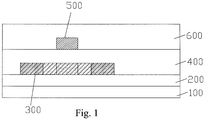
- As shown in
Figures 1-3 , the known TFT substrate manufacturing method comprises the following steps: - Step 1: as shown in
Figure 1 , providing abase substrate 100, and forming, in subsequent order of, abuffer layer 200, anactive layer 300, agate insulation layer 400, agate 500, and an interlayerdielectric layer 600; - Step 2: as shown in
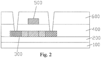
Figure 2 , performing etching simultaneously on the interlayerdielectric layer 600 and thegate insulation layer 400 to form vias on the interlayerdielectric layer 600 and thegate insulation layer 400 respectively corresponding to two ends of theactive layer 300; - Step 3: as shown in
Figure 3 , forming on the interlayerdielectric layer 600, in subsequent order of, asource 700 and adrain 800, aplanarization layer 900, acommon electrode 1000, apassivation layer 1100, and apixel electrode 1200. - In
Step 2 of the above TFT substrate manufacturing method, the process of performing simultaneous etching on the interlayerdielectric layer 600 and thegate insulation layer 400 is difficult to control because the interlayerdielectric layer 600 and thegate insulation layer 400 have a total thickness, which easily leads to non-penetrating vias or over-etching vias damaging theactive layer 300, resulting in product defects. Therefore, it is imperative to devise an improve TFT substrate manufacturing method to address the above issue. - The object of the present invention is to provide a TFT substrate manufacturing method, able to improve the active layer uniformity, reduce process difficulty, avoid the problem of etching stopped due to higher etching thickness, and improve the product quality.
- Another object of the present invention is to provide a TFT substrate, able to improve the active layer uniformity, reduce process difficulty, avoid the problem of etching stopped due to higher etching thickness, and improve the product quality.
- To achieve the above object, the present invention provides a thin film transistor (TFT) substrate manufacturing method, comprising:
- Step 1: providing a base substrate, and forming, in subsequent order of, a buffer layer and an active layer on the base substrate; performing ion doping at two ends of the active layer to form two ion heavily doped areas; forming a gate insulation layer on the active layer and the buffer layer;
- Step 2: forming a photo-resist layer on the gate insulation layer, performing etching and exposure with a half tone mask on the photo-resist layer to form a first groove and two first vias on the photo-resist layer; the first groove being located above a channel area to be formed between the two ion heavily doped areas, and the two first vias being located respectively above the two ion heavily doped areas;
- Step 3: using the remaining photo-resist layer as shielding to perform etching on the gate insulation layer to form two first through-holes at locations corresponding respectively to below the two first vias;
- Step 4: performing an overall thinning process on the photo-resist layer to transform the first groove into a second via;
using the remaining photo-resist layer as shielding to perform ion doping on the active layer to form a channel at locations below the second via; - Step 5: peeling the remaining photo-resist layer, depositing a first metal layer on the gate insulation layer, performing patternizing on the first metal layer to obtain a gate corresponding to a location above the channel, and two bridging metal blocks located respectively inside the two first through-holes;
- Step 6: using the gate as shielding to perform ion doping on the active layer to obtain two ion lightly doped areas located respectively between the channel and the two ion heavily doped areas;
- Step 7: forming an interlayer dielectric layer on the gate insulation layer, performing etching on the interlayer dielectric layer to form two second through-holes respectively above the two bridging metal blocks;
- Step 8: depositing a second metal layer on the interlayer dielectric layer, performing patternizing on the second metal layer to obtain a source and a drain distributed with a gap on the interlayer dielectric layer, the source and the drain contacting the two bridging metal blocks through the two through-holes;
- Step 9: forming on the interlayer dielectric layer, in subsequent order of, a planarization layer, a common voltage, a passivation layer, and a pixel electrode, stacked from bottom up.
- According to a preferred embodiment of the present invention, the etching on the gate insulation layer in Step 3 and the etching on the interlayer dielectric layer in
Step 7 are both dry etching. - According to a preferred embodiment of the present invention, in
Step 4, the overall thinning processing on the photo-resist layer is a photo-resist ashing method. - According to a preferred embodiment of the present invention, the pixel electrode contacts the drain through a third through-hole penetrating the planarization layer and the passivation layer.
- According to a preferred embodiment of the present invention, the base substrate is a glass substrate; the buffer layer, gate insulation layer, interlayer dielectric layer, and passivation layer are all made of a combination of one or more of silicon nitride(SiNx) and silicon oxide (SiOx); the active layer is made of polysilicon; the gate and the bridging metal blocks are made of at least one or alloy of molybdenum (Mo), aluminum (Al), copper (Cu), titanium (Ti), and tungsten (W); the planarization layer is made of a transparent organic insulation material; and the common electrode and the pixel electrode are made of indium tin oxide (ITO).
- The present invention also provides a thin film transistor (TFT) substrate, comprising: a base substrate, a buffer layer covering the base substrate, an active layer disposed on the buffer layer, a gate insulation layer covering the active layer and the buffer layer, two first through-holes penetrating the gate insulation layer, two bridging metal blocks respectively inside the two first through-holes, a gate disposed on the gate insulation layer, an interlayer dielectric layer covering the gate and the gate insulation layer, two second through-holes penetrating the interlayer dielectric layer, a source and a drain distributed with a gap disposed on the interlayer dielectric layer, and a planarization layer, a common electrode, a passivation layer, and a pixel electrode, stacked from the bottom up, disposed on the source, drain and the interlayer dielectric layer;
the active layer comprising: a channel, two ion heavily doped areas located respectively at two sides of the channel, and two ion lightly doped areas located respectively between the channel and the two ion heavily doped areas;
the two first through-holes being located respectively above the two ion heavily doped areas, the two bridging metal blocks contacting respectively the two ion heavily doped areas, and the gate being located on the gate insulation layer above the channel;
the two second through-holes connected respective the two first through-holes, and the source and the drain contacting the two bridging metal blocks through the two second through-holes respectively. - According to a preferred embodiment of the present invention, the pixel electrode contacts the drain through a third through-hole penetrating the planarization layer and the passivation layer.
- According to a preferred embodiment of the present invention, the first through-holes are obtained by separately performing dry etching on the gate insulation layer; the second through-holes are obtained by separately performing dry etching on the interlayer dielectric layer.
- According to a preferred embodiment of the present invention, the base substrate is a glass substrate; the buffer layer, gate insulation layer, interlayer dielectric layer, and passivation layer are all made of a combination of one or more of silicon nitride(SiNx) and silicon oxide (SiOx); the active layer is made of polysilicon; the gate and the bridging metal blocks are made of at least one or alloy of molybdenum (Mo), aluminum (Al), copper (Cu), titanium (Ti), and tungsten (W); the planarization layer is made of a transparent organic insulation material; and the common electrode and the pixel electrode are made of indium tin oxide (ITO).
- The present invention further provides a thin film transistor (TFT) substrate manufacturing method, comprising:
- Step 1: providing a base substrate, and forming, in subsequent order of, a buffer layer and an active layer on the base substrate; performing ion doping at two ends of the active layer to form two ion heavily doped areas; forming a gate insulation layer on the active layer and the buffer layer;
- Step 2: forming a photo-resist layer on the gate insulation layer, performing etching and exposure with a half tone mask on the photo-resist layer to form a first groove and two first vias on the photo-resist layer; the first groove being located above a channel area to be formed between the two ion heavily doped areas, and the two first vias being located respectively above the two ion heavily doped areas;
- Step 3: using the remaining photo-resist layer as shielding to perform etching on the gate insulation layer to form two first through-holes at locations corresponding respectively to below the two first vias;
- Step 4: performing an overall thinning process on the photo-resist layer to transform the first groove into a second via;
using the remaining photo-resist layer as shielding to perform ion doping on the active layer to form a channel at locations below the second via; - Step 5: peeling the remaining photo-resist layer, depositing a first metal layer on the gate insulation layer, performing patternizing on the first metal layer to obtain a gate corresponding to a location above the channel, and two bridging metal blocks located respectively inside the two first through-holes;
- Step 6: using the gate as shielding to perform ion doping on the active layer to obtain two ion lightly doped areas located respectively between the channel and the two ion heavily doped areas;
- Step 7: forming an interlayer dielectric layer on the gate insulation layer, performing etching on the interlayer dielectric layer to form two second through-holes respectively above the two bridging metal blocks;
- Step 8: depositing a second metal layer on the interlayer dielectric layer, performing patternizing on the second metal layer to obtain a source and a drain distributed with a gap on the interlayer dielectric layer, the source and the drain contacting the two bridging metal blocks through the two through-holes;
- Step 9: forming on the interlayer dielectric layer, in subsequent order of, a planarization layer, a common voltage, a passivation layer, and a pixel electrode, stacked from bottom up;
wherein the etching on the gate insulation layer in Step 3 and the etching on the interlayer dielectric layer inStep 7 being both dry etching;
wherein inStep 4, the overall thinning processing on the photo-resist layer being a photo-resist ashing method. - Compared to the known techniques, the present invention provides the following advantages: the present invention provides a TFT substrate manufacturing method, first etching the gate insulation layer to form two first through-holes and forming two bridging metal blocks in the two first through-holes, then etching the interlayer dielectric layer to form two second through-holes connecting the two first through-holes respectively, the source and drain contacting two bridging metal blocks through two second through-holes respectively. By changing an etching process in conventional process into two etching processes separately on the gate insulation layer and interlayer dielectric layer to improve the uniformity of the active layer, reduce the process difficulty, avoid the problem of etching stopped due to higher etching thickness, and improve the product quality. The present invention also provides a TFT substrate, able to improve the uniformity of the active layer, reduce the process difficulty, avoid the problem of etching stopped due to higher etching thickness, and improve the product quality.
- To make the technical solution of the embodiments according to the present invention, a brief description of the drawings that are necessary for the illustration of the embodiments will be given as follows. Apparently, the drawings described below show only example embodiments of the present invention and for those having ordinary skills in the art, other drawings may be easily obtained from these drawings without paying any creative effort. In the drawings:
-
Figure 1 is a schematic view showing Step 1 of a known TFT substrate manufacturing method; -
Figure 2 is a schematic view showingStep 2 of a known TFT substrate manufacturing method; -
Figure 3 is a schematic view showing Step 3 of a known TFT substrate manufacturing method; -
Figure 4 is schematic view showing the flowchart of the TFT substrate manufacturing method according to the present invention; -
Figure 5 is schematic view showing Step 1 of the TFT substrate manufacturing method according to the present invention; -
Figure 6 is schematic view showingStep 2 of the TFT substrate manufacturing method according to the present invention; -
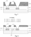
Figure 7 is schematic view showing Step 3 of the TFT substrate manufacturing method according to the present invention; -
Figure 8 is schematicview showing Step 4 of the TFT substrate manufacturing method according to the present invention; -
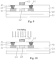
Figure 9 is schematicview showing Step 5 of the TFT substrate manufacturing method according to the present invention; -
Figure 10 is schematic view showing Step 6 of the TFT substrate manufacturing method according to the present invention; -
Figure 11 is schematicview showing Step 7 of the TFT substrate manufacturing method according to the present invention; -
Figure 12 is schematic view showing Step 8 of the TFT substrate manufacturing method according to the present invention; -
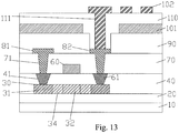
Figure 13 is a schematicview showing Step 9 of the manufacturing method of TFT substrate, and the TFT substrate structure according to the present invention. - To further explain the technical means and effect of the present invention, the following refers to embodiments and drawings for detailed description.
- Refer to
Figure 4 , the present invention provides a thin film transistor (TFT) substrate manufacturing method, comprising: - Step 1: as shown in
Figure 5 , providing abase substrate 10, and forming, in subsequent order of, abuffer layer 20 and anactive layer 30 on thebase substrate 10;
performing ion doping at two ends of theactive layer 30 to form two ion heavily dopedareas 31;
forming agate insulation layer 40 on theactive layer 30 and thebuffer layer 20.
Specifically, thebase substrate 10 is a glass substrate.
Specifically, thebuffer layer 20 is made of a combination of one or more of silicon nitride (SiNx) and silicon oxide (SiOx).
Specifically, theactive layer 30 is made of polysilicon.
Specifically, in Step 1, a mask is used to perform ion doping on the two ends of theactive layer 30. - Step 2: as shown in
Figure 6 , forming a photo-resistlayer 50 on thegate insulation layer 40, performing etching and exposure with a half tone mask on the photo-resistlayer 50 to form afirst groove 51 and twofirst vias 52 on the photo-resistlayer 50; thefirst groove 51 being located above a channel area to be formed between the two ion heavily dopedareas 31, and the twofirst vias 52 being located respectively above the two ion heavily dopedareas 31;
Specifically, thegate insulation layer 40 is made of a combination of one or more of silicon nitride (SiNx) and silicon oxide (SiOx). - Step 3: as shown in
Figure 7 , using the remaining photo-resistlayer 50 as shielding to perform etching on thegate insulation layer 40 to form two first through-holes 41 at locations corresponding respectively to below the twofirst vias 41.
Specifically, the etching on thegate insulation layer 40 is dry etching.
Specifically, because the gate insulation layer is relatively thinner, the etching process is easier to control to achieve uniformity and not prone to non-penetrating vias or over-etching vias causing the inconsistent loss to theactive layer 30; thus, improving product quality. - Step 4: as shown in
Figure 8 , performing an overall thinning process on the photo-resistlayer 50 to transform thefirst groove 51 into a second via 53;
using the remaining photo-resistlayer 50 as shielding to perform ion doping on theactive layer 30 to form achannel 32 at locations below the second via 53.
Specifically, inStep 4, the overall thinning processing on the photo-resistlayer 50 is a photo-resist ashing method. - Step 5: as shown in
Figure 9 , peeling the remaining photo-resistlayer 50, depositing a first metal layer on thegate insulation layer 40, performing patternizing on the first metal layer to obtain agate 60 corresponding to the location above thechannel 32, and two bridgingmetal blocks 61 located respectively inside the two first through-holes 41.
Specifically, thegate 60 and the bridgingmetal blocks 61 are made of at least one or alloy of molybdenum (Mo), aluminum (Al), copper (Cu), titanium (Ti), and tungsten (W). - Step 6: as shown in
Figure 10 , without using a mask, using thegate 60 as shielding to perform ion doping on theactive layer 30 to obtain two ion lightly doped areas 35 located respectively between thechannel 32 and the two ion heavily dopedareas 31. - Step 7: as shown in
Figure 11 , forming aninterlayer dielectric layer 70 on thegate insulation layer 40, performing etching on theinterlayer dielectric layer 70 to form two second through-holes 71 respectively above the two bridging metal blocks 61.
Specifically, the etching on the interlayer dielectric layer inStep 7 is dry etching.
Specifically, because the bottom layer of the second through-holes 71 is the bridgingmetal blocks 61, it is not necessary to concern about the loss of theactive layer 30 when etching, and the process window is large, which can effectively reduce the process difficulty, avoid the problem of etching stopped due to higher etching thickness, and improve the product quality.
Specifically, theinterlayer dielectric layer 70 is made of a combination of one or more of silicon nitride (SiNx) and silicon oxide (SiOx). - Step 8: as shown in
Figure 12 , depositing a second metal layer on theinterlayer dielectric layer 70, performing patternizing on the second metal layer to obtain asource 81 and adrain 82 distributed with a gap on theinterlayer dielectric layer 70, thesource 81 and thedrain 82 contacting the two bridgingmetal blocks 61 through the two through-holes 71. - Step 9: as shown in
Figure 13 , forming on theinterlayer dielectric layer 70, in subsequent order of, aplanarization layer 90, acommon voltage 101, apassivation layer 110, and a pixel electrode 103, stacked from bottom up. - Specifically, in
Step 9, a third through-hole 111 is formed on thepassivation layer 110 andplanarization layer 90 at a location above thedrain 82, and thepixel electrode 102 contacts thedrain 82 through the third through-hole 111. - Specifically, the
planarization layer 90 is made of a transparent organic insulation material. - Specifically, the
common electrode 101 and the pixel electrode102 are made of indium tin oxide (ITO). - Specifically, the
passivation layer 110 is made of a combination of one or more of silicon nitride (SiNx) and silicon oxide (SiOx). - The above TFT substrate manufacturing method changes an etching process in conventional process into two etching processes separately on the
gate insulation layer 40 andinterlayer dielectric layer 70; the first is to etch thegate insulation layer 40; because thegate insulation layer 40 is relatively thinner, the etching process is easier to control to achieve uniformity and not prone to non-penetrating vias or over-etching vias causing the inconsistent loss to theactive layer 30; then to etch theinterlayer dielectric layer 70, because the bottom layer of the second through-holes 71 is the bridgingmetal blocks 61, it is not necessary to concern about the loss of theactive layer 30 when etching, and the process window is large, which can effectively reduce the process difficulty, avoid the problem of etching stopped due to higher etching thickness, and improve the product quality. - Refer to
Figure 13 , based on the above TFT substrate manufacturing method, the present invention also provides a TFT substrate, comprising: abase substrate 10, abuffer layer 20 covering thebase substrate 10, anactive layer 30 disposed on thebuffer layer 20, agate insulation layer 40 covering theactive layer 30 and thebuffer layer 20, two first through-holes 41 penetrating thegate insulation layer 40, two bridgingmetal blocks 61 respectively inside the two first through-holes 41, agate 60 disposed on thegate insulation layer 40, aninterlayer dielectric layer 70 covering thegate 60 and thegate insulation layer 40, two second through-holes 71 penetrating theinterlayer dielectric layer 70, asource 81 and adrain 82 distributed with a gap disposed on theinterlayer dielectric layer 70, and aplanarization layer 90, acommon electrode 101, apassivation layer 110, and apixel electrode 102, stacked from the bottom up, disposed on thesource 81, drain 82 and theinterlayer dielectric layer 70;
theactive layer 30 comprising: achannel 32, two ion heavily dopedareas 31 located respectively at two sides of thechannel 32, and two ion lightly dopedareas 34 located respectively between thechannel 32 and the two ion heavily dopedareas 31;
the two first through-holes 41 being located respectively above the two ion heavily dopedareas 31, the two bridgingmetal blocks 61 contacting respectively the two ion heavily dopedareas 31, and thegate 60 being located on thegate insulation layer 40 above thechannel 40;
the two second through-holes 71 connected respective the two first through-holes 41, and thesource 81 and thedrain 82 contacting the two bridgingmetal 61 blocks through the two second through-holes 71 respectively. Specifically, the first through-holes 41 are obtained by separately performing dry etching on thegate insulation layer 40. - Specifically, the second through-
holes 71 are obtained by separately performing dry etching on theinterlayer dielectric layer 70. - Specifically, the
pixel electrode 102 contacts thedrain 82 through a third through-hole 111 penetrating theplanarization layer 90 and thepassivation layer 110. - Specifically, the base substrate is a glass substrate.
- Specifically, the
buffer layer 20,gate insulation layer 40,interlayer dielectric layer 70, andpassivation layer 110 are all made of a combination of one or more of silicon nitride (SiNx) and silicon oxide (SiOx). - Specifically, the
active layer 30 is made of polysilicon. - Specifically, the
gate 60 and the bridgingmetal blocks 61 are made of at least one or alloy of molybdenum (Mo), aluminum (Al), copper (Cu), titanium (Ti), and tungsten (W). - Specifically, the
planarization layer 90 is made of a transparent organic insulation material. - Specifically, the
common electrode 101 and thepixel electrode 102 are made of indium tin oxide (ITO). - The above TFT substrate changes the one through-hole structure in conventional
gate insulation layer 40 andinterlayer dielectric layer 70 into a two through-hole structure; the first is to etch thegate insulation layer 40; because thegate insulation layer 40 is relatively thinner, the etching process is easier to control to achieve uniformity and not prone to non-penetrating vias or over-etching vias causing the inconsistent loss to theactive layer 30; then to etch theinterlayer dielectric layer 70, because the bottom layer of the second through-holes 71 is the bridgingmetal blocks 61, which avoids the effect on theactive layer 30 when etching, and the process window is large, which can effectively reduce the process difficulty, avoid the problem of etching stopped due to higher etching thickness, and improve the product quality. - In summary, the present invention provides a TFT substrate manufacturing method and TFT substrate; first etching the gate insulation layer to form two first through-holes and forming two bridging metal blocks inside the two first through holes; then etching the interlayer dielectric layer to form two second through-holes connecting respectively the two first through-holes, the source and drain connecting the two bridging metal blocks respectively through the two second through-holes. By changing a conventional etching process into two etching process to form the through-hole structure on the gate insulation layer and interlayer dielectric layer, able to improve uniformity of the active layer, reduce process difficulty, avoid the problem of etching stopped due to higher etching thickness, and improve the product quality.
- Embodiments of the present invention have been described, but not intending to impose any unduly constraint to the appended claims. Any modification of equivalent structure or equivalent process made according to the disclosure and drawings of the present invention, or any application thereof, directly or indirectly, to other related fields of technique, is considered encompassed in the scope of protection defined by the clams of the present invention.
Claims (12)
- A thin film transistor (TFT) substrate manufacturing method, comprising the steps of:Step 1: providing a base substrate, and forming, in subsequent order of, a buffer layer and an active layer on the base substrate; performing ion doping at two ends of the active layer to form two ion heavily doped areas; forming a gate insulation layer on the active layer and the buffer layer;Step 2: forming a photo-resist layer on the gate insulation layer, performing etching and exposure with a half tone mask on the photo-resist layer to form a first groove and two first vias on the photo-resist layer; the first groove being located above a channel area to be formed between the two ion heavily doped areas, and the two first vias being located respectively above the two ion heavily doped areas;Step 3: using the remaining photo-resist layer as shielding to perform etching on the gate insulation layer to form two first through-holes at locations corresponding respectively to below the two first vias;Step 4: performing an overall thinning process on the photo-resist layer to transform the first groove into a second via;
using the remaining photo-resist layer as shielding to perform ion doping on the active layer to form a channel at locations below the second via;Step 5: peeling the remaining photo-resist layer, depositing a first metal layer on the gate insulation layer, performing patternizing on the first metal layer to obtain a gate corresponding to a location above the channel, and two bridging metal blocks located respectively inside the two first through-holes;Step 6: using the gate as shielding to perform ion doping on the active layer to obtain two ion lightly doped areas located respectively between the channel and the two ion heavily doped areas;Step 7: forming an interlayer dielectric layer on the gate insulation layer, performing etching on the interlayer dielectric layer to form two second through-holes respectively above the two bridging metal blocks;Step 8: depositing a second metal layer on the interlayer dielectric layer, performing patternizing on the second metal layer to obtain a source and a drain distributed with a gap on the interlayer dielectric layer, the source and the drain contacting the two bridging metal blocks through the two through-holes;Step 9: forming on the interlayer dielectric layer, in subsequent order of, a planarization layer, a common electrode, a passivation layer, and a pixel electrode, stacked from bottom up. - The TFT substrate manufacturing method as claimed in Claim 1, wherein the etching on the gate insulation layer in Step 3 and the etching on the interlayer dielectric layer in Step 7 are both dry etching.
- The TFT substrate manufacturing method as claimed in Claim 1, wherein in Step 4, the overall thinning processing on the photo-resist layer is a photo-resist ashing method.
- The TFT substrate manufacturing method as claimed in Claim 1, wherein the pixel electrode contacts the drain through a third through-hole penetrating the planarization layer and the passivation layer.
- The TFT substrate manufacturing method as claimed in Claim 1, wherein the base substrate is a glass substrate; the buffer layer, gate insulation layer, interlayer dielectric layer, and passivation layer are all made of a combination of one or more of silicon nitride (SiNx) and silicon oxide (SiOx); the active layer is made of polysilicon; the gate and the bridging metal blocks are made of at least one or alloy of molybdenum (Mo), aluminum (Al), copper (Cu), titanium (Ti), and tungsten (W); the planarization layer is made of a transparent organic insulation material; and the common electrode and the pixel electrode are made of indium tin oxide (ITO).
- A thin film transistor (TFT) substrate, comprising: a base substrate, a buffer layer covering the base substrate, an active layer disposed on the buffer layer, a gate insulation layer covering the active layer and the buffer layer, two first through-holes penetrating the gate insulation layer, two bridging metal blocks respectively inside the two first through-holes, a gate disposed on the gate insulation layer, an interlayer dielectric layer covering the gate and the gate insulation layer, two second through-holes penetrating the interlayer dielectric layer, a source and a drain distributed with a gap disposed on the interlayer dielectric layer, and a planarization layer, a common electrode, a passivation layer, and a pixel electrode, stacked from the bottom up, disposed on the source, drain and the interlayer dielectric layer;
the active layer comprising: a channel, two ion heavily doped areas located respectively at two sides of the channel, and two ion lightly doped areas located respectively between the channel and the two ion heavily doped areas;
the two first through-holes being located respectively above the two ion heavily doped areas, the two bridging metal blocks contacting respectively the two ion heavily doped areas, and the gate being located on the gate insulation layer above the channel;
the two second through-holes connected respective the two first through-holes, and the source and the drain contacting the two bridging metal blocks through the two second through-holes respectively. - The TFT substrate as claimed in Claim 6, wherein, the pixel electrode contacts the drain through a third through-hole penetrating the planarization layer and the passivation layer.
- The TFT substrate as claimed in Claim 6, wherein the first through-holes are obtained by separately performing dry etching on the gate insulation layer; the second through-holes are obtained by separately performing dry etching on the interlayer dielectric layer.
- The TFT substrate as claimed in Claim 6, wherein the base substrate is a glass substrate; the buffer layer, gate insulation layer, interlayer dielectric layer, and passivation layer are all made of a combination of one or more of silicon nitride (SiNx) and silicon oxide (SiOx); the active layer is made of polysilicon; the gate and the bridging metal blocks are made of at least one or alloy of molybdenum (Mo), aluminum (Al), copper (Cu), titanium (Ti), and tungsten (W); the planarization layer is made of a transparent organic insulation material; and the common electrode and the pixel electrode are made of indium tin oxide (ITO).
- A thin film transistor (TFT) substrate manufacturing method, comprising the steps of:Step 1: providing a base substrate, and forming, in subsequent order of, a buffer layer and an active layer on the base substrate; performing ion doping at two ends of the active layer to form two ion heavily doped areas; forming a gate insulation layer on the active layer and the buffer layer;Step 2: forming a photo-resist layer on the gate insulation layer, performing etching and exposure with a half tone mask on the photo-resist layer to form a first groove and two first vias on the photo-resist layer; the first groove being located above a channel area to be formed between the two ion heavily doped areas, and the two first vias being located respectively above the two ion heavily doped areas;Step 3: using the remaining photo-resist layer as shielding to perform etching on the gate insulation layer to form two first through-holes at locations corresponding respectively to below the two first vias;Step 4: performing an overall thinning process on the photo-resist layer to transform the first groove into a second via;
using the remaining photo-resist layer as shielding to perform ion doping on the active layer to form a channel at locations below the second via;Step 5: peeling the remaining photo-resist layer, depositing a first metal layer on the gate insulation layer, performing patternizing on the first metal layer to obtain a gate corresponding to a location above the channel, and two bridging metal blocks located respectively inside the two first through-holes;Step 6: using the gate as shielding to perform ion doping on the active layer to obtain two ion lightly doped areas located respectively between the channel and the two ion heavily doped areas;Step 7: forming an interlayer dielectric layer on the gate insulation layer, performing etching on the interlayer dielectric layer to form two second through-holes respectively above the two bridging metal blocks;Step 8: depositing a second metal layer on the interlayer dielectric layer, performing patternizing on the second metal layer to obtain a source and a drain distributed with a gap on the interlayer dielectric layer, the source and the drain contacting the two bridging metal blocks through the two through-holes;Step 9: forming on the interlayer dielectric layer, in subsequent order of, a planarization layer, a common voltage, a passivation layer, and a pixel electrode, stacked from bottom up;wherein the etching on the gate insulation layer in Step 3 and the etching on the interlayer dielectric layer in Step 7 being both dry etching;wherein in Step 4, the overall thinning processing on the photo-resist layer being a photo-resist ashing method. - The TFT substrate manufacturing method as claimed in Claim 10, wherein the pixel electrode contacts the drain through a third through-hole penetrating the planarization layer and the passivation layer.
- The TFT substrate manufacturing method as claimed in Claim 10, wherein the base substrate is a glass substrate; the buffer layer, gate insulation layer, interlayer dielectric layer, and passivation layer are all made of a combination of one or more of silicon nitride (SiNx) and silicon oxide (SiOx); the active layer is made of polysilicon; the gate and the bridging metal blocks are made of at least one or alloy of molybdenum (Mo), aluminum (Al), copper (Cu), titanium (Ti), and tungsten (W); the planarization layer is made of a transparent organic insulation material; and the common electrode and the pixel electrode are made of indium tin oxide (ITO).
Applications Claiming Priority (2)
| Application Number | Priority Date | Filing Date | Title |
|---|---|---|---|
| CN201710218699.2A CN107039351B (en) | 2017-04-05 | 2017-04-05 | The production method and TFT substrate of TFT substrate |
| PCT/CN2017/084601 WO2018184279A1 (en) | 2017-04-05 | 2017-05-16 | Tft substrate and manufacturing method thereof |
Publications (2)
| Publication Number | Publication Date |
|---|---|
| EP3608950A1 true EP3608950A1 (en) | 2020-02-12 |
| EP3608950A4 EP3608950A4 (en) | 2020-12-23 |
Family
ID=59534835
Family Applications (1)
| Application Number | Title | Priority Date | Filing Date |
|---|---|---|---|
| EP17904463.1A Withdrawn EP3608950A4 (en) | 2017-04-05 | 2017-05-16 | TFT SUBSTRATE AND MANUFACTURING METHOD FOR IT |
Country Status (5)
| Country | Link |
|---|---|
| US (1) | US10181484B2 (en) |
| EP (1) | EP3608950A4 (en) |
| KR (1) | KR102314509B1 (en) |
| CN (1) | CN107039351B (en) |
| WO (1) | WO2018184279A1 (en) |
Cited By (1)
| Publication number | Priority date | Publication date | Assignee | Title |
|---|---|---|---|---|
| US12501663B2 (en) | 2020-04-03 | 2025-12-16 | Samsung Electronics Co., Ltd. | Display module including zinc-based barrier pattern and method for manufacturing same |
Families Citing this family (12)
| Publication number | Priority date | Publication date | Assignee | Title |
|---|---|---|---|---|
| CN108073331A (en) * | 2018-02-26 | 2018-05-25 | 武汉华星光电技术有限公司 | The preparation method of array substrate, touching display screen and array substrate |
| CN108598089B (en) * | 2018-04-27 | 2020-09-29 | 武汉华星光电技术有限公司 | TFT substrate manufacturing method and TFT substrate |
| CN110321031B (en) * | 2019-06-28 | 2024-04-12 | 福建华佳彩有限公司 | Embedded touch panel and manufacturing method thereof |
| CN110600424B (en) * | 2019-08-20 | 2023-08-01 | 武汉华星光电技术有限公司 | Array substrate preparation method and array substrate |
| TWI715344B (en) * | 2019-12-10 | 2021-01-01 | 友達光電股份有限公司 | Active device substrate and manufacturing method thereof |
| CN111668239B (en) * | 2020-06-19 | 2022-11-08 | 武汉华星光电半导体显示技术有限公司 | OLED display panel and preparation method |
| CN112490275B (en) * | 2020-12-03 | 2023-04-21 | 湖北长江新型显示产业创新中心有限公司 | Display panel, manufacturing method thereof and display device |
| CN114447119B (en) * | 2022-01-20 | 2026-02-06 | 广州华星光电半导体显示技术有限公司 | TFT substrate and manufacturing method thereof |
| CN114900778B (en) * | 2022-05-15 | 2024-09-17 | 中北大学 | Composite film electromagnetic shielding capacitive acoustic transducer and manufacturing method thereof |
| CN115207002A (en) * | 2022-07-21 | 2022-10-18 | 福建华佳彩有限公司 | Oxide thin film transistor array substrate with lower stress and preparation method |
| CN116207104A (en) * | 2022-11-14 | 2023-06-02 | 武汉华星光电技术有限公司 | Display panel and preparation method thereof |
| CN116544244B (en) * | 2023-06-21 | 2024-07-05 | 惠科股份有限公司 | Array substrate and display panel |
Family Cites Families (20)
| Publication number | Priority date | Publication date | Assignee | Title |
|---|---|---|---|---|
| JP4730994B2 (en) * | 1999-06-04 | 2011-07-20 | 株式会社半導体エネルギー研究所 | Electro-optical device, manufacturing method thereof, and electronic device |
| KR100307456B1 (en) * | 1999-12-08 | 2001-10-17 | 김순택 | Method for manufacturing Thin Film Transistor |
| US6995048B2 (en) * | 2001-05-18 | 2006-02-07 | Sanyo Electric Co., Ltd. | Thin film transistor and active matrix type display unit production methods therefor |
| JP4275346B2 (en) | 2002-03-08 | 2009-06-10 | 株式会社半導体エネルギー研究所 | Method for manufacturing semiconductor device |
| US7064021B2 (en) * | 2003-07-02 | 2006-06-20 | Au Optronics Corp. | Method for fomring a self-aligned LTPS TFT |
| JP4677713B2 (en) * | 2003-11-25 | 2011-04-27 | セイコーエプソン株式会社 | Electro-optical device substrate, method for manufacturing electro-optical device substrate, electro-optical device, and electronic apparatus |
| TWI401802B (en) * | 2005-06-30 | 2013-07-11 | 三星電子股份有限公司 | Thin film transistor plate and method of manufacturing same |
| KR20070117269A (en) * | 2006-06-08 | 2007-12-12 | 삼성전자주식회사 | Display device and manufacturing method thereof |
| KR101002665B1 (en) * | 2008-07-02 | 2010-12-21 | 삼성모바일디스플레이주식회사 | Thin film transistor, manufacturing method thereof and organic light emitting display device comprising same |
| JP2010272691A (en) | 2009-05-21 | 2010-12-02 | Sharp Corp | Thin film transistor substrate manufacturing method, thin film transistor substrate, and display device |
| KR101284287B1 (en) * | 2010-12-21 | 2013-07-08 | 엘지디스플레이 주식회사 | Liquid crystal display device and method for manufacturing the same |
| KR102207063B1 (en) * | 2012-12-12 | 2021-01-25 | 엘지디스플레이 주식회사 | Thin film transistor, method for manufacturing the same and display device comprising the same |
| US10642116B2 (en) * | 2013-05-01 | 2020-05-05 | Apple Inc. | Display pixels with improved storage capacitance |
| KR102136992B1 (en) * | 2013-07-12 | 2020-07-24 | 삼성디스플레이 주식회사 | Thin film transistor, and thin film transistor array panel and organic light emitting diode display including the same |
| WO2015153648A1 (en) * | 2014-03-31 | 2015-10-08 | Ingredients By Nature | Flavonoid compositions and uses thereof |
| CN104022077B (en) * | 2014-05-27 | 2017-01-25 | 京东方科技集团股份有限公司 | Array substrate, preparing method thereof and display device |
| CN105489480B (en) * | 2014-09-16 | 2019-01-08 | 中芯国际集成电路制造(上海)有限公司 | The method that grid is formed using Dual graphing technology |
| KR102303433B1 (en) * | 2014-11-24 | 2021-09-17 | 삼성디스플레이 주식회사 | Organic light emitting diode display and method for manufacturing thereof |
| CN104637874A (en) * | 2015-03-16 | 2015-05-20 | 京东方科技集团股份有限公司 | Array base plate and manufacturing method thereof |
| CN105895581B (en) * | 2016-06-22 | 2019-01-01 | 武汉华星光电技术有限公司 | The production method of TFT substrate |
-
2017
- 2017-04-05 CN CN201710218699.2A patent/CN107039351B/en active Active
- 2017-05-16 WO PCT/CN2017/084601 patent/WO2018184279A1/en not_active Ceased
- 2017-05-16 EP EP17904463.1A patent/EP3608950A4/en not_active Withdrawn
- 2017-05-16 KR KR1020197032764A patent/KR102314509B1/en active Active
- 2017-05-16 US US15/544,023 patent/US10181484B2/en active Active
Cited By (1)
| Publication number | Priority date | Publication date | Assignee | Title |
|---|---|---|---|---|
| US12501663B2 (en) | 2020-04-03 | 2025-12-16 | Samsung Electronics Co., Ltd. | Display module including zinc-based barrier pattern and method for manufacturing same |
Also Published As
| Publication number | Publication date |
|---|---|
| US20180294293A1 (en) | 2018-10-11 |
| CN107039351A (en) | 2017-08-11 |
| US10181484B2 (en) | 2019-01-15 |
| KR102314509B1 (en) | 2021-10-18 |
| KR20190131582A (en) | 2019-11-26 |
| WO2018184279A1 (en) | 2018-10-11 |
| CN107039351B (en) | 2019-10-11 |
| EP3608950A4 (en) | 2020-12-23 |
Similar Documents
| Publication | Publication Date | Title |
|---|---|---|
| US10181484B2 (en) | TFT substrate manufacturing method and TFT substrate | |
| US10120247B2 (en) | Manufacturing method for TFT substrate and TFT substrate manufactured by the manufacturing method thereof | |
| US9947754B1 (en) | Manufacturing method of array substrate and LCD panel | |
| US10338440B2 (en) | TFT substrate and manufacturing method thereof | |
| CN101419945A (en) | Manufacturing method of semiconductor device | |
| US11239331B2 (en) | Thin film transistor substrate and method of fabricating same | |
| US11114475B2 (en) | IPS thin-film transistor array substrate and manufacturing method thereof | |
| US10347662B2 (en) | Array substrate, manufacturing method thereof, and display panel | |
| US10254609B2 (en) | Array substrate including pixel electrode and drain electrode in direct contact to each other, and method of manufacturing the same, display panel, and display device | |
| CN113467145A (en) | Array substrate, manufacturing method and display panel | |
| US20160254288A1 (en) | Array substrate and manufacturing method thereof, display device | |
| CN111679517A (en) | Display panel, manufacturing method thereof and display device | |
| CN104020621B (en) | A kind of array base palte and preparation method thereof, display device | |
| US10211232B2 (en) | Manufacture method of array substrate and array substrate manufactured by the method | |
| WO2024065111A1 (en) | Array substrate and manufacturing method therefor, and display panel | |
| US10644036B2 (en) | VA type TFT array substrate and the manufacturing method thereof | |
| US10551696B2 (en) | Method of producing metal electrode, array substrate and method of producing the same, display device | |
| WO2020082460A1 (en) | Method for manufacturing display panel, and display panel | |
| US12405501B2 (en) | Liquid crystal display panel and manufacturing method thereof | |
| CN116699912B (en) | Array substrate, preparation method thereof, display panel and display device | |
| US20230369353A1 (en) | Display panel and manufacturing method thereof | |
| KR0146251B1 (en) | Thin film transistor manufacturing method for liquid crystal device | |
| CN109659314B (en) | Array substrate and manufacturing method thereof | |
| KR100492728B1 (en) | A liquid crystal display device having partially removed activation layer in drain region and method of fabricating thereof | |
| KR0146249B1 (en) | Thin film transistor and its manufacturing method for liquid crystal display device |
Legal Events
| Date | Code | Title | Description |
|---|---|---|---|
| STAA | Information on the status of an ep patent application or granted ep patent |
Free format text: STATUS: THE INTERNATIONAL PUBLICATION HAS BEEN MADE |
|
| PUAI | Public reference made under article 153(3) epc to a published international application that has entered the european phase |
Free format text: ORIGINAL CODE: 0009012 |
|
| STAA | Information on the status of an ep patent application or granted ep patent |
Free format text: STATUS: REQUEST FOR EXAMINATION WAS MADE |
|
| 17P | Request for examination filed |
Effective date: 20191105 |
|
| AK | Designated contracting states |
Kind code of ref document: A1 Designated state(s): AL AT BE BG CH CY CZ DE DK EE ES FI FR GB GR HR HU IE IS IT LI LT LU LV MC MK MT NL NO PL PT RO RS SE SI SK SM TR |
|
| AX | Request for extension of the european patent |
Extension state: BA ME |
|
| DAV | Request for validation of the european patent (deleted) | ||
| DAX | Request for extension of the european patent (deleted) | ||
| REG | Reference to a national code |
Ref country code: DE Ref legal event code: R079 Free format text: PREVIOUS MAIN CLASS: H01L0021840000 Ipc: H01L0027120000 |
|
| A4 | Supplementary search report drawn up and despatched |
Effective date: 20201124 |
|
| RIC1 | Information provided on ipc code assigned before grant |
Ipc: H01L 29/786 20060101ALI20201118BHEP Ipc: H01L 27/12 20060101AFI20201118BHEP |
|
| GRAP | Despatch of communication of intention to grant a patent |
Free format text: ORIGINAL CODE: EPIDOSNIGR1 |
|
| STAA | Information on the status of an ep patent application or granted ep patent |
Free format text: STATUS: GRANT OF PATENT IS INTENDED |
|
| INTG | Intention to grant announced |
Effective date: 20230321 |
|
| RIN1 | Information on inventor provided before grant (corrected) |
Inventor name: YANG, LING Inventor name: ZHANG, ZHANDONG Inventor name: ZHANG, HAIJIE |
|
| P01 | Opt-out of the competence of the unified patent court (upc) registered |
Effective date: 20230530 |
|
| STAA | Information on the status of an ep patent application or granted ep patent |
Free format text: STATUS: THE APPLICATION IS DEEMED TO BE WITHDRAWN |
|
| 18D | Application deemed to be withdrawn |
Effective date: 20230801 |