EP3608944A1 - Methods for removing nuclei formed during epitaxial growth - Google Patents
Methods for removing nuclei formed during epitaxial growth Download PDFInfo
- Publication number
- EP3608944A1 EP3608944A1 EP19188206.7A EP19188206A EP3608944A1 EP 3608944 A1 EP3608944 A1 EP 3608944A1 EP 19188206 A EP19188206 A EP 19188206A EP 3608944 A1 EP3608944 A1 EP 3608944A1
- Authority
- EP
- European Patent Office
- Prior art keywords
- group
- semiconductor structures
- semiconductor
- structures
- subset
- Prior art date
- Legal status (The legal status is an assumption and is not a legal conclusion. Google has not performed a legal analysis and makes no representation as to the accuracy of the status listed.)
- Pending
Links
Images





Classifications
-
- H—ELECTRICITY
- H10—SEMICONDUCTOR DEVICES; ELECTRIC SOLID-STATE DEVICES NOT OTHERWISE PROVIDED FOR
- H10P—GENERIC PROCESSES OR APPARATUS FOR THE MANUFACTURE OR TREATMENT OF DEVICES COVERED BY CLASS H10
- H10P50/00—Etching of wafers, substrates or parts of devices
- H10P50/69—Etching of wafers, substrates or parts of devices using masks for semiconductor materials
- H10P50/691—Etching of wafers, substrates or parts of devices using masks for semiconductor materials for Group V materials or Group III-V materials
- H10P50/692—Etching of wafers, substrates or parts of devices using masks for semiconductor materials for Group V materials or Group III-V materials characterised by their composition, e.g. multilayer masks or materials
-
- H—ELECTRICITY
- H10—SEMICONDUCTOR DEVICES; ELECTRIC SOLID-STATE DEVICES NOT OTHERWISE PROVIDED FOR
- H10P—GENERIC PROCESSES OR APPARATUS FOR THE MANUFACTURE OR TREATMENT OF DEVICES COVERED BY CLASS H10
- H10P14/00—Formation of materials, e.g. in the shape of layers or pillars
- H10P14/20—Formation of materials, e.g. in the shape of layers or pillars of semiconductor materials
- H10P14/27—Formation of materials, e.g. in the shape of layers or pillars of semiconductor materials using selective deposition, e.g. simultaneous growth of monocrystalline and non-monocrystalline semiconductor materials
-
- H—ELECTRICITY
- H10—SEMICONDUCTOR DEVICES; ELECTRIC SOLID-STATE DEVICES NOT OTHERWISE PROVIDED FOR
- H10P—GENERIC PROCESSES OR APPARATUS FOR THE MANUFACTURE OR TREATMENT OF DEVICES COVERED BY CLASS H10
- H10P50/00—Etching of wafers, substrates or parts of devices
- H10P50/60—Wet etching
- H10P50/64—Wet etching of semiconductor materials
- H10P50/642—Chemical etching
-
- H—ELECTRICITY
- H10—SEMICONDUCTOR DEVICES; ELECTRIC SOLID-STATE DEVICES NOT OTHERWISE PROVIDED FOR
- H10P—GENERIC PROCESSES OR APPARATUS FOR THE MANUFACTURE OR TREATMENT OF DEVICES COVERED BY CLASS H10
- H10P70/00—Cleaning of wafers, substrates or parts of devices
- H10P70/20—Cleaning during device manufacture
-
- H—ELECTRICITY
- H10—SEMICONDUCTOR DEVICES; ELECTRIC SOLID-STATE DEVICES NOT OTHERWISE PROVIDED FOR
- H10P—GENERIC PROCESSES OR APPARATUS FOR THE MANUFACTURE OR TREATMENT OF DEVICES COVERED BY CLASS H10
- H10P70/00—Cleaning of wafers, substrates or parts of devices
- H10P70/50—Cleaning of wafers, substrates or parts of devices characterised by the part to be cleaned
Definitions
- This application relates generally to methods for manufacturing semiconductor devices. More particularly, the disclosed embodiments relate to methods for removing nuclei formed on semiconductor devices during epitaxial growth processes.
- Epitaxial growth is a popular method of creating a crystalline region on a semiconductor substrate.
- formation of semiconductor structures in unwanted regions of the semiconductor substrate is undesirable.
- any semiconductor structures grown in unwanted regions of the semiconductor substrate can adversely affect the electrical and/or mechanical properties of a device formed on the substrate.
- Selective epitaxial growth is used for creating a crystalline region on targeted areas of the semiconductor substrate.
- a semiconductor substrate is covered with a masking material, exposing certain areas of the underlying substrate.
- the epitaxial growth occurs mainly on the exposed areas of the semiconductor substrate, and less so on the masking material.
- the selective epitaxial growth may reduce formation of structures (e.g., in the form of nuclei or layers) on the masking material during the epitaxial growth, depending on the process conditions, many semiconductor structures may still form on the masking material during the epitaxial growth.
- the methods would be less-sensitive to changes to the growth conditions.
- improved methods would also enable faster epitaxial growth of semiconductor structures while reducing the formation of semiconductor structures on unwanted regions of the substrate during the epitaxial growth.
- some embodiments involve a method for removing nuclei formed during a selective epitaxial growth process that includes epitaxially growing a first group of one or more semiconductor structures on a substrate with one or more mask layers. A second group of a plurality of semiconductor structures is formed on the one or more mask layers. The method also includes forming one or more protective layers over the first group of one or more semiconductor structures. At least a subset of the second group of the plurality of semiconductor structures is exposed from the one or more protective layers. The method further includes, subsequent to forming the one or more protective layers over the first group of one or more semiconductor structures, etching at least the subset of the second group of the plurality of semiconductor structures.
- a semiconductor device in accordance with some embodiments, includes a substrate; a first mask layer region that is located over the substrate; and a second mask layer region that is located over the substrate.
- the first mask layer region has a top surface and a lateral surface
- the second mask layer region has a top surface and a lateral surface.
- the semiconductor device also includes an epitaxially grown semiconductor structure of a first semiconductor material type. The epitaxially grown semiconductor structure is located between the lateral surface of the first mask layer region and the lateral surface of the second mask layer region, and the epitaxially grown semiconductor structure is in contact with the lateral surface of the first mask layer region and the lateral surface of the second mask layer region.
- the top surface of the first mask layer region and the top surface of the second mask layer region are not in contact with a semiconductor of the first semiconductor material type other than the epitaxially grown semiconductor structure located between the lateral surface of the first mask layer region and the lateral surface of the second mask layer region.
- the substrate is exposed to an etchant (e.g., an HCl gas) during the epitaxial growth (e.g., by mixing the HCl gas with a deposition gas), thereby allowing etching of the unwanted semiconductor structures during the epitaxial growth.
- an etchant e.g., an HCl gas
- the etchant e.g., an HCl gas
- the etchant affects the speed of epitaxially growing semiconductor structures.
- the rate of forming the target semiconductor structures is impeded by the etching reaction, and thus, is slower than the rate of forming the target semiconductor structures in the absence of the etchant.
- the reduced rate of forming the target semiconductor structure can be a bottleneck in the overall device fabrication process.
- the presence of an etchant affects the shape of the epitaxially grown semiconductor structures.
- a ratio of a growth rate in a dominant direction to a growth rate in a non-dominant direction is increased significantly. For example, in germanium epitaxial growth, (100) is the dominant growth direction.
- the resulting epitaxially grown germanium structures have a pyramid shape with (311) slope.
- the presence of the etchant makes it more challenging to obtain semiconductor structures with shapes different from the pyramid shape.
- germanium having the pyramid shape with (311) slope is formed to cover a certain area, the height of the germanium pyramid can be high, which makes it challenging to obtain a planarized surface (e.g., by using a chemical mechanical planarization (CMP) process).
- CMP chemical mechanical planarization
- lowering the temperature and pressure during the epitaxial growth is believed to reduce formation of the unwanted semiconductor structures during the epitaxial growth.
- lowering the deposition temperature decreases the crystallinity of the grown semiconductor structures, which lead to increased leakage current in the semiconductor device.
- Lowering the pressure can lead to a lower deposition rate and increase the roughness of the semiconductor structures, which will degrade the performance of the fabricated device.
- germane gas GeH 4
- H 2 hydrogen gas
- the semiconductor structures By epitaxially growing semiconductor structures with no (or less) etchant, the semiconductor structures can be grown faster. In addition, the shape of the semiconductor structures is less affected by the etchant, because no (or less) etchant is present during the epitaxial growth. Furthermore, the pressure and/or temperature need not be lowered during the epitaxial growth. Although the epitaxial growth with no (or less) etchant (and at the normal pressure and temperature) will lead to formation of semiconductor structures on unwanted regions, such as on the masking material, such semiconductor structures on the unwanted regions are subsequently removed by an etching process. Thus, semiconductor structures epitaxially grown in target areas of the substrate can be obtained with no or reduced semiconductor structures grown in the unwanted regions.
- first, second, etc. may be used herein to describe various elements, these elements should not be limited by these terms. These terms are only used to distinguish one element from another. For example, a first group could be termed a second group, and, similarly, a second group could be termed a first group, without departing from the scope of the claims.
- the first group and the second group are both groups (e.g., of semiconductor structures), but they are not the same group.
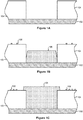
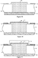
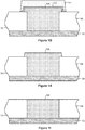
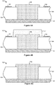
- Figures 1A-1I are partial cross-sectional views of a semiconductor substrate in accordance with some embodiments.
- Figure 1A illustrates a substrate 102 and a mask layer 104 on the substrate 102.
- the substrate 102 is shown as a wafer in Figures 1A-1I , 2A-2C , 3A-3C , 4A-4C , and 5A-5E , the substrate 102 may include additional features not shown in Figures 1A-1I , 2A-2C , 3A-3C , 4A-4C , and 5A-5E .
- the substrate 102 includes silicon devices (e.g., silicon complementary metal-oxide-semiconductor devices as well as any other structures typically formed during the front-end of the line (FEOL) processes).
- the substrate 102 includes an oxide layer on the silicon devices (e.g., Figures 6A-6B ).
- the mask layer 104 includes a dielectric material (e.g., silicon dioxide). In some embodiments, the mask layer 104 is made of a dielectric material (e.g., silicon dioxide). The mask layer 104 exposes one or more portions of the substrate 102. In some embodiments, the dielectric material is deposited on the substrate 102 and subsequently etched to expose the one or more portions of the substrate 102. In some embodiments, the substrate 102 is further etched. In some cases, this further etching provides a surface more suitable for epitaxial growth.
- a dielectric material e.g., silicon dioxide
- the mask layer 104 is made of a dielectric material (e.g., silicon dioxide).
- the mask layer 104 exposes one or more portions of the substrate 102. In some embodiments, the dielectric material is deposited on the substrate 102 and subsequently etched to expose the one or more portions of the substrate 102. In some embodiments, the substrate 102 is further etched. In some cases, this further etching provides a surface
- Figure 1B illustrates that a semiconductor structure 106 (e.g., a germanium island) is epitaxially grown.
- the conditions e.g., pressure, temperature, and chemical composition
- the methods described herein do not require the use of an etchant (e.g., HCl gas) to suppress growth of semiconductor structures on the mask layer 104 during the epitaxial growth, although the use of an etchant is not precluded.
- the conditions for epitaxial growth can be adjusted to obtain the desired growth profile. Thus, it is possible to customize the shape of the epitaxially grown semiconductor structures.
- Figure 1B also illustrates that semiconductor structures 108 (e.g., particles, which are also called herein nuclei) are also formed on the mask layer 104 during the epitaxial growth of the semiconductor structure 106.
- the semiconductor structures 108 typically have amorphous and/or poly-crystalline structures, whereas the semiconductor structure 106 has a crystalline structure.
- Figure 1C illustrates that the semiconductor structure 106 continues to grow. Figure 1C also illustrates that additional semiconductor structures 108 are formed on the mask layer 104.
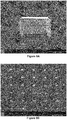
- Figures 8A and 8B are scanning electron microscope (SEM) images of a substrate after epitaxial growth of a germanium island, which are described in detail below.
- Figure 1D illustrates that the semiconductor structures 108 are aggregated to form a film 110 in some embodiments.
- Figure 1E illustrates that optionally, an adhesive layer 112 is applied (e.g., deposited) over the substrate 102.
- the adhesive layer 112 covers the semiconductor structure 106 and the film 110 on the mask layer 104.
- the adhesive layer 112 is a low-thermal oxide.
- the adhesive layer 112 is hexamethyldisilazane (HMDS).
- HMDS hexamethyldisilazane
- the adhesive layer 112 promotes adhesion between the epitaxially grown semiconductor structure 106 and photoresist.
- Figure IF illustrates a protective layer 114 (e.g., a photo resist layer) is applied over the substrate 102.
- the protective layer 114 covers a portion of the adhesive layer 112 over the semiconductor structure 106.
- the protective layer 114 does not cover the film 110 (e.g., the film 110 is exposed from the protective layer 114, although the film 110 is covered with the adhesive layer 112).
- Figure 1G illustrates that regions not covered by the protective layer 114 have been etched.
- the film 110 (and any other unwanted semiconductor structures formed during the epitaxial growth of the semiconductor structure 106) is removed.
- a portion of the adhesive layer 112 located over the film 110 is also removed.
- a selective etching process which removes the film 110 (and any other unwanted semiconductor structures formed during the epitaxial growth of the semiconductor structure 106) faster than protective layer 114, is used (such etching processes are called to have high selectivity) so that the semiconductor structure 106 is maintained while the film 110 and/or any other unwanted semiconductor structures formed during the epitaxial growth of the semiconductor structure 106 are removed.
- the etching process is a dry etching process (e.g., plasma etching, deep reactive ion etching, etc.). In some embodiments, the etching process is a wet etching process (e.g., etching with liquid-phase etchants). For example, an advanced silicon etching instrument manufactured by Surface Technology Systems Plc. may be used for the selective etching.
- Figure 1H illustrates that the protective layer 114 and the adhesive layer 112 are removed.
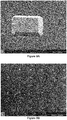
- Figures 9A and 9B are scanning electron microscope (SEM) images of a substrate after removing the protective layer 114, which are described in detail below.
- Figure 1I illustrates that the semiconductor structure 106 is planarized (e.g., using a CMP process). Because the unwanted semiconductor structures (e.g., nuclei 108 or film 110) have been removed, a CMP process can be readily applied. In addition, because the shape of the semiconductor structure 106 can be adjusted to have a flat top, it is easier to perform a CMP process.
- a CMP process can be readily applied.
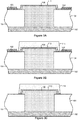
- Figures 2A-2C are partial cross-sectional views of a semiconductor substrate in accordance with some embodiments.
- Figures 2A-2C are similar to those illustrated in Figures 1F-1H except that the optional adhesive layer 112 ( Figure 1E ) is not used.
- Figure 2A illustrates that the protective layer 114 is applied directly on the semiconductor structure 106 shown in Figure 1D .
- Figure 2B illustrates that regions not covered by the protective layer 114 have been etched, which is similar to the process described above with respect to Figure 1G .
- the film 110 (and any other unwanted semiconductor structures formed during the epitaxial growth of the semiconductor structure 106) is removed.
- Figure 2C illustrates that the protective layer 114 is removed, which is similar to the process described above with respect to Figure 1H . Subsequently, the semiconductor structure 106 can be planarized, as described above with respect to Figure 1I .
- Figures 3A-3C are partial cross-sectional views of a semiconductor substrate in accordance with some embodiments.
- Figure 3A illustrates that the adhesive layer 112 is applied over the semiconductor structure 106 and the semiconductor structures 108 (e.g., particles) on the mask layer 104, which is analogous to the process described above with respect to Figure 1E .
- Figure 3B illustrates that the protective layer 114 is applied over the substrate 102, which is analogous to the process described above with respect to Figure IF.
- Figure 3C illustrates that regions not covered by the protective layer 114 have been etched, which is similar to the process described above with respect to Figure 1G .
- the semiconductor structures 108 are removed.
- a portion of the adhesive layer 112 located over the semiconductor structures 108 is also removed.
- the semiconductor substrate illustrated in Figure 3C is further processed as described above with respect to Figures 1H and 1I .
- the protective layer 114 and the adhesive layer 112 are removed and the semiconductor structure 106 is planarized to obtain the semiconductor substrate illustrated in Figure 1I .
- Figures 4A-4C are partial cross-sectional views of a semiconductor substrate in accordance with some embodiments.
- Figure 4A illustrates that the protective layer 114 is applied directly on the semiconductor structure 106 before the semiconductor structures 108 are aggregated.
- Figure 4B illustrates that regions not covered by the protective layer 114 have been etched, which is similar to the process described above with respect to Figure 2B . As a result of etching, the semiconductor structures 108 are removed.
- Figure 4C illustrates that the protective layer 114 is removed, which is similar to the process illustrated described above with respect to Figure 2C . Subsequently, the semiconductor structure 106 can be planarized, as described above with respect to Figure 1I .
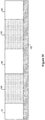
- Figures 5A-5E are partial cross-sectional views of a semiconductor substrate in accordance with some embodiments.
- Figures 5A-5E clarify that the processes illustrated in Figures 1A-1I can be performed in forming multiple semiconductor structures (e.g., germanium islands) on a single semiconductor substrate.
- multiple semiconductor structures e.g., germanium islands
- Figure 5A illustrates that semiconductor structures 106 are epitaxially grown and that semiconductor structures 108 are formed on the mask layer 104.
- Figure 5B illustrates that a protective layer 114 is applied on the semiconductor structures 106 while exposing the semiconductor structures 108.
- Figure 5C illustrates that the semiconductor structures 108 are removed by etching.
- Figure 5D illustrates that the protective layer 114 is removed.
- Figure 5E illustrates that the semiconductor structures 106 are planarized (e.g., using a CMP process).
- the adhesive layer 112 may be applied over the semiconductor structures 106 before the protective layer 114 is applied (or formed) over the semiconductor structures 106. For brevity, such details are not repeated herein.
- Figures 6A-6B are partial cross-sectional views of a semiconductor substrate in accordance with some embodiments.
- Figure 6A illustrates that the substrate 102 includes complementary metal-oxide-semiconductor (CMOS) devices with source/drains 602 and gates 604.
- CMOS complementary metal-oxide-semiconductor
- a mask layer 606 e.g., silicon dioxide
- the mask layer 606 includes silicon dioxide of at least 2 ⁇ m thickness, for growing a germanium layer thereon. The thickness of the silicon dioxide was found to improve the quality of the crystallinity of the epitaxially grown germanium.
- Figure 6B illustrates that a semiconductor structure 608 (e.g., germanium) is formed using the processes described above with respect to Figures 1A-1I , 2A-2C , 3A-3C , 4A-4C , and 5A-5E .
- a semiconductor structure 608 e.g., germanium
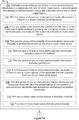
- Figures 7A-7C are flow diagrams illustrating a method 700 of removing nuclei formed during a selective epitaxial growth process in accordance with some embodiments.
- the method 700 includes (702) epitaxially growing a first group of one or more semiconductor structures (e.g., the semiconductor structure 106 in Figure 1B ) over a substrate (e.g., a silicon substrate) with one or more mask layers (e.g., the substrate 102 with the mask layer 104 in Figure 1B ).
- a second group of a plurality of semiconductor structures e.g., semiconductor structures 108 in Figure 1B
- the second group of the plurality of semiconductor structures is formed concurrently with epitaxially growing the first group of the one or more semiconductor structures.
- a first semiconductor structure of the first group of one or more semiconductor structures is larger than a second semiconductor structure of the second group of the plurality of semiconductor structures.
- the one or more semiconductor structures are homo-epitaxially grown. In some embodiments, the one or more semiconductor structures are hetero-epitaxially grown.
- the first group of the one or more semiconductor structures is formed (704) in a single epitaxial growth process.
- the semiconductor structure 106 is formed in a single epitaxial growth process (e.g., instead of epitaxially growing a portion of the semiconductor structure 106, etching a portion of the semiconductor structure 106, and epitaxially growing an additional portion of the semiconductor structure 106).
- the method 700 includes (706) forming a plurality of semiconductor particles (e.g., the semiconductor structures 108 in Figure 1C ) on the one or more mask layers (e.g., the mask layer 104 in Figure 1C ) while epitaxially growing the first group of one or more semiconductor structures (e.g., the semiconductor structure 106 in Figure 1C ) on the substrate with one or more mask layers.
- the second group of the plurality of semiconductor structures includes the plurality of semiconductor particles.
- the second group of the plurality of semiconductor structures includes (708) a semiconductor film (e.g., the semiconductor film 110 in Figure 1D ) on the one or more mask layers. In some embodiments, the second group of the plurality of semiconductor structures includes one or more semiconductor films on the one or more mask layers.
- the first group of one or more semiconductor structures includes (710) a column IV material (e.g., silicon, germanium, SiGe, etc.). In some embodiments, the first group of one or more semiconductor structures includes one or more III-V materials (e.g., GaAs, InGaAs, etc.).
- the first group of one or more semiconductor structures includes (712) germanium.
- the first group of one or more semiconductor structures is formed (714) on one or more regions of the substrate that are exposed from the one or more mask layers (e.g., not covered by the one or more mask layers).
- the semiconductor structures 106 are formed on the regions of the substrate that are exposed from the mask layer 104.
- the first group of one or more semiconductor structures has (716) crystalline structures and the second group of the plurality of semiconductor structures has amorphous and/or poly-crystalline structures.
- Figure 8A shows that the first group of one or more semiconductor structures (e.g., the germanium island) has a crystalline structure and the second group of semiconductor structures has amorphous and/or poly-crystalline structures.
- the one or more mask layers include (718) a dielectric material.
- the one or more mask layers include (720) silicon dioxide.
- the method 700 also includes (722, Figure 7B ) forming one or more protective layers (e.g., the protective layer 114 in Figure IF, such as one or more photoresist layers) over the first group of one or more semiconductor structures. At least a subset of the second group of the plurality of semiconductor structures is exposed from the one or more protective layers. For example, in Figure IF, the film 110 is exposed from the protective layer 114.
- the one or more protective layers are in direct contact with the first group of one or more semiconductor structures (e.g., Figure 2A ).
- one or more intermediate layers e.g., one or more adhesive layers, such as hexamethyldisilazane (HMDS) or low-temperature thermal oxide
- HMDS hexamethyldisilazane
- Figure IF one or more protective layers
- the method 700 includes (724) foregoing etching at least the subset of the second group of the plurality of semiconductor structures before the one or more protective layers are formed over the first group of one or more semiconductor structures.
- the second group of the plurality of semiconductor structures is not etched until after the one or more protective layers are formed over the one or more semiconductor structures to protect the one or more semiconductor structures from the etching process.
- the method 700 includes (726) foregoing etching at least the subset of the second group of the plurality of semiconductor structures subsequent to initiating the epitaxial growth of the first group of one or more semiconductor structures on the substrate until the one or more protective layers are formed over the first group of one or more semiconductor structures.
- etching of at least the subset of the second group of the plurality of semiconductor structures is foregone during the epitaxial growth of the first group of one or more semiconductor structures.
- etching at least the subset of the plurality of semiconductor structures is foregone after initiating the epitaxial growth of the first group of one or more semiconductor structures on the substrate and before forming the one or more protective layers over the one or more semiconductor structures.
- the one or more protective layers include (728) one or more photoresist layers. In some embodiments, the one or more protective layers are one or more photoresist layers.
- the method 700 includes (730) depositing one or more adhesive layers over at least the first group of one or more semiconductor structures prior to forming the one or more protective layers.
- the adhesive layer 112 is applied over the semiconductor structure 106 before the protective layer 114 is applied.
- the one or more adhesive layers are deposited on at least the first group of one or more semiconductor structures.
- the one or more adhesive layers include (732) hexamethyldisilazane and/or low-temperature thermal oxide.
- the method includes, subsequent to etching at least the subset of the second group of the plurality of semiconductor structures, removing the one or more adhesive layers.
- the one or more protective layers and the one or more adhesive layers are removed concurrently.
- the one or more protective layers are removed subsequent to removing the one or more adhesive layers.
- the substrate includes silicon. In some embodiments, the substrate is a silicon substrate.
- the substrate includes (734) a plurality of semiconductor devices thereon (e.g., Figures 6A-6B ).
- the substrate may include a plurality of transistors prior to epitaxially growing the first group of one or more semiconductor structures.
- the substrate includes a plurality of transistors and a semiconductor structure of the first group of one or more semiconductor structures is electrically coupled to a source or a drain of a transistor of the plurality of transistors.
- the substrate includes (736) a plurality of complementary metal-oxide semiconductor (CMOS) devices thereon (e.g., Figures 6A-6B ).
- CMOS complementary metal-oxide semiconductor
- the substrate includes thereon a plurality of complementary metal-oxide semiconductor devices, including a p-type metal-oxide-semiconductor transistor and an n-type metal-oxide-semiconductor transistor.
- the method includes electrically coupling a first semiconductor structure of the first group of one or more semiconductor structures to a source or a drain of one of: the p-type metal-oxide-semiconductor transistor or the n-type metal-oxide-semiconductor transistor.
- the plurality of semiconductor devices is located (738) on the substrate below the one or more mask layers.
- the semiconductor devices e.g., transistors
- the plurality of semiconductor devices is located in the front-end of the line (FEOL) region of the substrate.
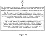
- the method 700 further includes (740, Figure 7C ), subsequent to forming the one or more protective layers over the first group of one or more semiconductor structures, etching at least the subset of the second group of the plurality of semiconductor structures.
- the film 110 is removed due to the etching process.
- at least the subset of the plurality of semiconductor structures that is exposed from the one or more photoresist layers is completely etched (e.g., removed).
- at least the subset of the plurality of semiconductor structures that is exposed from the one or more photoresist layers is at least partially etched (e.g., removed).
- one or more semiconductor structures of at least the subset of the plurality of semiconductor structures that is exposed from the one or more photoresist layers are etched (e.g., removed). In some embodiments, the entire second group of the plurality of semiconductor structures formed on the one or more mask layers is etched (e.g., removed).
- the method includes etching the entire subset of the second group of the plurality of semiconductor structures that is exposed from the one or more protective layers.
- the method 700 includes (742), subsequent to etching at least the subset of the second group of the plurality of semiconductor structures, removing the one or more protective layers (e.g., Figure 1H ) and/or planarizing at least a subset of the first group of one or more semiconductor structures (e.g., using chemical-mechanical planarization).
- the method 700 includes, subsequent to etching at least the subset of the second group of the plurality of semiconductor structures, removing the one or more protective layers.
- the method 700 includes, subsequent to etching at least the subset of the second group of the plurality of semiconductor structures, planarizing at least a subset of the first group of one or more semiconductor structures. For example, in Figure 1I , the semiconductor structure 106 is planarized.
- etching at least the subset of the second group of the plurality of semiconductor structures includes (744) etching at least the subset of the second group of the plurality of semiconductor structures at a first rate and etching the one or more mask layers at a second rate that is lower than the first rate.
- the film 110 is etched faster than the mask layer 104 and the protective layer 114.
- etching at least the subset of the second group of the plurality of semiconductor structures includes etching at least the subset of the second group of the plurality of semiconductor structures without etching the one or more mask layers.
- the film 110 shown in Figure IF is etched while the mask layer 104 and the protective layer 114 are not etched.
- etching at least the subset of the second group of the plurality of semiconductor structures includes foregoing etching of the one or more mask layers.
- etching at least the subset of the second group of the plurality of semiconductor structures includes (744) etching at least the subset of the second group of the plurality of semiconductor structures at a first rate and etching at least a subset of the first group of one or more semiconductor structures at a third rate that is lower than the first rate.
- the film 110 is etched faster than the semiconductor structure 106.
- etching at least the subset of the second group of the plurality of semiconductor structures includes etching at least the subset of the second group of the plurality of semiconductor structures without etching the first group of one or more semiconductor structures.
- the film 110 shown in Figure IF is etched while the semiconductor structure 106 is not etched (e.g., because the semiconductor structure 106 is protected by the protective layer 114).
- Figures 8A-8B are scanning electron microscope (SEM) images of a semiconductor substrate prior to an etching process in accordance with some embodiments.
- FIGS 8A and 8B Shown in Figures 8A and 8B are top-down views of the semiconductor substrate that corresponds to Figure 1C .
- Figure 8A shows a germanium island that corresponds to the semiconductor structure 106 in Figure 1C (before the etching process).
- the second group of semiconductor structures is formed around the germanium island on the mask layer.
- Figure 8B is a zoomed-out view of the semiconductor substrate. Multiple germanium islands and the second group of semiconductor structures formed on the mask layer are shown in Figure 8B .
- Figures 9A-9B are scanning electron microscope (SEM) images of a semiconductor substrate subsequent to an etching process in accordance with some embodiments.
- Figure 9A shows a germanium island that corresponds to the semiconductor structure 106 in Figure 1H (after the etching process).
- Figure 9A shows the absence of the second group of semiconductor structures around the germanium island on the mask layer.
- Figure 9B is a zoomed-out view of the semiconductor substrate. Multiple germanium islands without the second group of semiconductor structures are shown in Figure 9B .
- Figures 9A-9B show the effectiveness of the described methods in removing the second group of semiconductor structures formed on the one or more mask layers.
Landscapes
- Recrystallisation Techniques (AREA)
- Chemical & Material Sciences (AREA)
- Chemical Kinetics & Catalysis (AREA)
- General Chemical & Material Sciences (AREA)
- Weting (AREA)
- Thin Film Transistor (AREA)
- Crystals, And After-Treatments Of Crystals (AREA)
- Chemical Vapour Deposition (AREA)
Applications Claiming Priority (4)
| Application Number | Priority Date | Filing Date | Title |
|---|---|---|---|
| US201562165816P | 2015-05-22 | 2015-05-22 | |
| US15/051,362 US9378950B1 (en) | 2015-05-22 | 2016-02-23 | Methods for removing nuclei formed during epitaxial growth |
| PCT/US2016/033783 WO2016191371A1 (en) | 2015-05-22 | 2016-05-23 | Methods for removing nuclei formed during epitaxial growth |
| EP16750355.6A EP3111466A4 (en) | 2015-05-22 | 2016-05-23 | Methods for removing nuclei formed during epitaxial growth |
Related Parent Applications (1)
| Application Number | Title | Priority Date | Filing Date |
|---|---|---|---|
| EP16750355.6A Division EP3111466A4 (en) | 2015-05-22 | 2016-05-23 | Methods for removing nuclei formed during epitaxial growth |
Publications (1)
| Publication Number | Publication Date |
|---|---|
| EP3608944A1 true EP3608944A1 (en) | 2020-02-12 |
Family
ID=56136460
Family Applications (2)
| Application Number | Title | Priority Date | Filing Date |
|---|---|---|---|
| EP19188206.7A Pending EP3608944A1 (en) | 2015-05-22 | 2016-05-23 | Methods for removing nuclei formed during epitaxial growth |
| EP16750355.6A Ceased EP3111466A4 (en) | 2015-05-22 | 2016-05-23 | Methods for removing nuclei formed during epitaxial growth |
Family Applications After (1)
| Application Number | Title | Priority Date | Filing Date |
|---|---|---|---|
| EP16750355.6A Ceased EP3111466A4 (en) | 2015-05-22 | 2016-05-23 | Methods for removing nuclei formed during epitaxial growth |
Country Status (6)
| Country | Link |
|---|---|
| US (1) | US9378950B1 (cg-RX-API-DMAC7.html) |
| EP (2) | EP3608944A1 (cg-RX-API-DMAC7.html) |
| JP (1) | JP6787786B2 (cg-RX-API-DMAC7.html) |
| KR (2) | KR102424567B1 (cg-RX-API-DMAC7.html) |
| CN (1) | CN106663598B (cg-RX-API-DMAC7.html) |
| WO (1) | WO2016191371A1 (cg-RX-API-DMAC7.html) |
Cited By (1)
| Publication number | Priority date | Publication date | Assignee | Title |
|---|---|---|---|---|
| FR3128819A1 (fr) * | 2021-11-02 | 2023-05-05 | Commissariat à l'Energie Atomique et aux Energies Alternatives | Procédé de traitement de surface |
Families Citing this family (3)
| Publication number | Priority date | Publication date | Assignee | Title |
|---|---|---|---|---|
| US10256093B2 (en) * | 2015-11-30 | 2019-04-09 | Alliance For Sustainable Energy, Llc | Selective area growth of semiconductors using patterned sol-gel materials |
| US10366884B1 (en) * | 2018-11-08 | 2019-07-30 | Stratio | Methods for forming a germanium island using selective epitaxial growth and a sacrificial filling layer |
| KR102763596B1 (ko) | 2019-03-25 | 2025-02-10 | 삼성전자주식회사 | 반도체 소자 |
Citations (4)
| Publication number | Priority date | Publication date | Assignee | Title |
|---|---|---|---|---|
| EP0352471A2 (en) * | 1988-07-27 | 1990-01-31 | Texas Instruments Incorporated | Method of planarising semiconductor devices |
| JPH08203833A (ja) * | 1995-01-20 | 1996-08-09 | Hitachi Ltd | 半導体装置の製造方法 |
| US20070287272A1 (en) * | 2006-06-07 | 2007-12-13 | Asm America, Inc. | Selective epitaxial formation of semiconductor films |
| EP2299475A1 (en) * | 2009-09-18 | 2011-03-23 | Taiwan Semiconductor Manufacturing Co., Ltd. | Improved fabrication and structures of crystalline material |
Family Cites Families (8)
| Publication number | Priority date | Publication date | Assignee | Title |
|---|---|---|---|---|
| JPH04188719A (ja) * | 1990-11-21 | 1992-07-07 | Mitsubishi Electric Corp | 選択埋込み成長法 |
| JPH0521357A (ja) * | 1991-07-10 | 1993-01-29 | Fujitsu Ltd | 半導体装置の製造方法 |
| US5981400A (en) * | 1997-09-18 | 1999-11-09 | Cornell Research Foundation, Inc. | Compliant universal substrate for epitaxial growth |
| WO2010061615A1 (ja) * | 2008-11-28 | 2010-06-03 | 住友化学株式会社 | 半導体基板の製造方法、半導体基板、電子デバイスの製造方法、および反応装置 |
| JP2011108692A (ja) * | 2009-11-12 | 2011-06-02 | Ulvac Japan Ltd | Cmosデバイス用シリコンウェハの製造方法 |
| CN103367553B (zh) * | 2012-03-28 | 2016-01-20 | 清华大学 | 外延衬底的制备方法 |
| JP5931780B2 (ja) * | 2013-03-06 | 2016-06-08 | 東京エレクトロン株式会社 | 選択エピタキシャル成長法および成膜装置 |
| JP2014181170A (ja) * | 2013-03-21 | 2014-09-29 | Mitsubishi Chemicals Corp | 半導体バルク結晶および半導体バルク結晶の製造方法 |
-
2016
- 2016-02-23 US US15/051,362 patent/US9378950B1/en active Active
- 2016-05-23 JP JP2016557040A patent/JP6787786B2/ja active Active
- 2016-05-23 KR KR1020187006394A patent/KR102424567B1/ko active Active
- 2016-05-23 CN CN201680000867.4A patent/CN106663598B/zh active Active
- 2016-05-23 EP EP19188206.7A patent/EP3608944A1/en active Pending
- 2016-05-23 KR KR1020177005543A patent/KR20170029638A/ko not_active Ceased
- 2016-05-23 WO PCT/US2016/033783 patent/WO2016191371A1/en not_active Ceased
- 2016-05-23 EP EP16750355.6A patent/EP3111466A4/en not_active Ceased
Patent Citations (4)
| Publication number | Priority date | Publication date | Assignee | Title |
|---|---|---|---|---|
| EP0352471A2 (en) * | 1988-07-27 | 1990-01-31 | Texas Instruments Incorporated | Method of planarising semiconductor devices |
| JPH08203833A (ja) * | 1995-01-20 | 1996-08-09 | Hitachi Ltd | 半導体装置の製造方法 |
| US20070287272A1 (en) * | 2006-06-07 | 2007-12-13 | Asm America, Inc. | Selective epitaxial formation of semiconductor films |
| EP2299475A1 (en) * | 2009-09-18 | 2011-03-23 | Taiwan Semiconductor Manufacturing Co., Ltd. | Improved fabrication and structures of crystalline material |
Non-Patent Citations (4)
| Title |
|---|
| AVENIER G ET AL: "0.13micrometer SiGe BiCMOS technology for mm-wave applications", BIPOLAR/BICMOS CIRCUITS AND TECHNOLOGY MEETING, 2008. BCTM 2008. IEEE, IEEE, PISCATAWAY, NJ, USA, 13 October 2008 (2008-10-13), pages 89 - 92, XP031355131, ISBN: 978-1-4244-2725-3 * |
| CRABBE E F ET AL: "Vertical profile optimization of very high frequency epitaxial Si- and SiGe-base bipolar transistors", ELECTRON DEVICES MEETING, 1993. TECHNICAL DIGEST., INTERNATIONAL WASHINGTON, DC, USA 5-8 DEC. 1993, NEW YORK, NY, USA,IEEE, 5 December 1993 (1993-12-05), pages 83 - 86, XP032365844, ISBN: 978-0-7803-1450-4, DOI: 10.1109/IEDM.1993.347393 * |
| HYDRICK J M ET AL: "Chemical Mechanical Polishing of Epitaxial Germanium on SiO2 patterned Si(001) Substrates", TRANSACTIONS OF THE ELECTROCHEMICAL SOCIETY, ELECTROCHEMICAL SOCIETY INC. MANCHESTER, US, vol. 16, no. 10, 1 January 2008 (2008-01-01), pages 237 - 248, XP009141658 * |
| PARK J-S ET AL: "Defect reduction of selective Ge epitaxy in trenches on Si(001) substrates using aspect ratio trapping", APPLIED PHYSICS LETTERS, AMERICAN INSTITUTE OF PHYSICS, 2 HUNTINGTON QUADRANGLE, MELVILLE, NY 11747, vol. 90, no. 5, 2 February 2007 (2007-02-02), pages 52113 - 052113, XP012095827, ISSN: 0003-6951, DOI: 10.1063/1.2435603 * |
Cited By (2)
| Publication number | Priority date | Publication date | Assignee | Title |
|---|---|---|---|---|
| FR3128819A1 (fr) * | 2021-11-02 | 2023-05-05 | Commissariat à l'Energie Atomique et aux Energies Alternatives | Procédé de traitement de surface |
| WO2023078692A1 (fr) * | 2021-11-02 | 2023-05-11 | Commissariat A L'energie Atomique Et Aux Energies Alternatives | Procede de traitement de surface |
Also Published As
| Publication number | Publication date |
|---|---|
| CN106663598B (zh) | 2018-08-07 |
| JP2018515904A (ja) | 2018-06-14 |
| WO2016191371A1 (en) | 2016-12-01 |
| EP3111466A1 (en) | 2017-01-04 |
| EP3111466A4 (en) | 2017-03-29 |
| US9378950B1 (en) | 2016-06-28 |
| JP6787786B2 (ja) | 2020-11-18 |
| KR20180029091A (ko) | 2018-03-19 |
| KR102424567B1 (ko) | 2022-07-25 |
| CN106663598A (zh) | 2017-05-10 |
| KR20170029638A (ko) | 2017-03-15 |
Similar Documents
| Publication | Publication Date | Title |
|---|---|---|
| KR102370595B1 (ko) | 자기 정렬식 대체 핀 형성 | |
| US10580901B2 (en) | Stacked series connected VFETs for high voltage applications | |
| US8999821B2 (en) | Fin formation by epitaxial deposition | |
| US9129938B1 (en) | Methods of forming germanium-containing and/or III-V nanowire gate-all-around transistors | |
| US8728927B1 (en) | Borderless contacts for semiconductor transistors | |
| US9299775B2 (en) | Methods for the production of integrated circuits comprising epitaxially grown replacement structures | |
| US9252014B2 (en) | Trench sidewall protection for selective epitaxial semiconductor material formation | |
| CN105097513B (zh) | 一种半导体器件的制造方法、半导体器件和电子装置 | |
| EP3608944A1 (en) | Methods for removing nuclei formed during epitaxial growth | |
| US20140191299A1 (en) | Dual Damascene Metal Gate | |
| US6972228B2 (en) | Method of forming an element of a microelectronic circuit | |
| US9620420B2 (en) | Semiconductor arrangement and formation thereof | |
| US20200373411A1 (en) | Bottom isolation by selective top deposition in gaa transistors | |
| TWI792157B (zh) | 半導體結構及其製造方法 | |
| US10103262B2 (en) | Method of forming a finFET structure with high quality EPI film | |
| CN114300362A (zh) | 一种半导体结构及其制造方法 | |
| HK1237991A1 (en) | Methods for removing nuclei formed during epitaxial growth | |
| HK1237991B (zh) | 用於去除在外延生长期间形成的核的方法 | |
| JP2018006410A (ja) | Iii−v族化合物の微細構造形成方法 |
Legal Events
| Date | Code | Title | Description |
|---|---|---|---|
| PUAI | Public reference made under article 153(3) epc to a published international application that has entered the european phase |
Free format text: ORIGINAL CODE: 0009012 |
|
| STAA | Information on the status of an ep patent application or granted ep patent |
Free format text: STATUS: THE APPLICATION HAS BEEN PUBLISHED |
|
| AC | Divisional application: reference to earlier application |
Ref document number: 3111466 Country of ref document: EP Kind code of ref document: P |
|
| AK | Designated contracting states |
Kind code of ref document: A1 Designated state(s): AL AT BE BG CH CY CZ DE DK EE ES FI FR GB GR HR HU IE IS IT LI LT LU LV MC MK MT NL NO PL PT RO RS SE SI SK SM TR |
|
| STAA | Information on the status of an ep patent application or granted ep patent |
Free format text: STATUS: REQUEST FOR EXAMINATION WAS MADE |
|
| 17P | Request for examination filed |
Effective date: 20200812 |
|
| RBV | Designated contracting states (corrected) |
Designated state(s): AL AT BE BG CH CY CZ DE DK EE ES FI FR GB GR HR HU IE IS IT LI LT LU LV MC MK MT NL NO PL PT RO RS SE SI SK SM TR |
|
| STAA | Information on the status of an ep patent application or granted ep patent |
Free format text: STATUS: EXAMINATION IS IN PROGRESS |
|
| 17Q | First examination report despatched |
Effective date: 20220103 |
|
| P01 | Opt-out of the competence of the unified patent court (upc) registered |
Effective date: 20230602 |