EP3605621A1 - Quantum dot led packaging structure - Google Patents
Quantum dot led packaging structure Download PDFInfo
- Publication number
- EP3605621A1 EP3605621A1 EP17903598.5A EP17903598A EP3605621A1 EP 3605621 A1 EP3605621 A1 EP 3605621A1 EP 17903598 A EP17903598 A EP 17903598A EP 3605621 A1 EP3605621 A1 EP 3605621A1
- Authority
- EP
- European Patent Office
- Prior art keywords
- quantum dot
- layer
- bracket
- emitting chip
- light emitting
- Prior art date
- Legal status (The legal status is an assumption and is not a legal conclusion. Google has not performed a legal analysis and makes no representation as to the accuracy of the status listed.)
- Granted
Links
Images

Classifications
-
- H—ELECTRICITY
- H10—SEMICONDUCTOR DEVICES; ELECTRIC SOLID-STATE DEVICES NOT OTHERWISE PROVIDED FOR
- H10H—INORGANIC LIGHT-EMITTING SEMICONDUCTOR DEVICES HAVING POTENTIAL BARRIERS
- H10H20/00—Individual inorganic light-emitting semiconductor devices having potential barriers, e.g. light-emitting diodes [LED]
- H10H20/80—Constructional details
- H10H20/81—Bodies
- H10H20/811—Bodies having quantum effect structures or superlattices, e.g. tunnel junctions
- H10H20/812—Bodies having quantum effect structures or superlattices, e.g. tunnel junctions within the light-emitting regions, e.g. having quantum confinement structures
-
- H—ELECTRICITY
- H10—SEMICONDUCTOR DEVICES; ELECTRIC SOLID-STATE DEVICES NOT OTHERWISE PROVIDED FOR
- H10H—INORGANIC LIGHT-EMITTING SEMICONDUCTOR DEVICES HAVING POTENTIAL BARRIERS
- H10H20/00—Individual inorganic light-emitting semiconductor devices having potential barriers, e.g. light-emitting diodes [LED]
- H10H20/80—Constructional details
- H10H20/84—Coatings, e.g. passivation layers or antireflective coatings
-
- H—ELECTRICITY
- H10—SEMICONDUCTOR DEVICES; ELECTRIC SOLID-STATE DEVICES NOT OTHERWISE PROVIDED FOR
- H10H—INORGANIC LIGHT-EMITTING SEMICONDUCTOR DEVICES HAVING POTENTIAL BARRIERS
- H10H20/00—Individual inorganic light-emitting semiconductor devices having potential barriers, e.g. light-emitting diodes [LED]
- H10H20/80—Constructional details
- H10H20/85—Packages
- H10H20/8506—Containers
-
- H—ELECTRICITY
- H10—SEMICONDUCTOR DEVICES; ELECTRIC SOLID-STATE DEVICES NOT OTHERWISE PROVIDED FOR
- H10H—INORGANIC LIGHT-EMITTING SEMICONDUCTOR DEVICES HAVING POTENTIAL BARRIERS
- H10H20/00—Individual inorganic light-emitting semiconductor devices having potential barriers, e.g. light-emitting diodes [LED]
- H10H20/80—Constructional details
- H10H20/85—Packages
- H10H20/851—Wavelength conversion means
- H10H20/8511—Wavelength conversion means characterised by their material, e.g. binder
- H10H20/8512—Wavelength conversion materials
-
- H—ELECTRICITY
- H10—SEMICONDUCTOR DEVICES; ELECTRIC SOLID-STATE DEVICES NOT OTHERWISE PROVIDED FOR
- H10H—INORGANIC LIGHT-EMITTING SEMICONDUCTOR DEVICES HAVING POTENTIAL BARRIERS
- H10H20/00—Individual inorganic light-emitting semiconductor devices having potential barriers, e.g. light-emitting diodes [LED]
- H10H20/80—Constructional details
- H10H20/85—Packages
- H10H20/851—Wavelength conversion means
- H10H20/8511—Wavelength conversion means characterised by their material, e.g. binder
- H10H20/8512—Wavelength conversion materials
- H10H20/8513—Wavelength conversion materials having two or more wavelength conversion materials
-
- H—ELECTRICITY
- H10—SEMICONDUCTOR DEVICES; ELECTRIC SOLID-STATE DEVICES NOT OTHERWISE PROVIDED FOR
- H10H—INORGANIC LIGHT-EMITTING SEMICONDUCTOR DEVICES HAVING POTENTIAL BARRIERS
- H10H20/00—Individual inorganic light-emitting semiconductor devices having potential barriers, e.g. light-emitting diodes [LED]
- H10H20/80—Constructional details
- H10H20/85—Packages
- H10H20/852—Encapsulations
- H10H20/853—Encapsulations characterised by their shape
-
- H—ELECTRICITY
- H10—SEMICONDUCTOR DEVICES; ELECTRIC SOLID-STATE DEVICES NOT OTHERWISE PROVIDED FOR
- H10H—INORGANIC LIGHT-EMITTING SEMICONDUCTOR DEVICES HAVING POTENTIAL BARRIERS
- H10H20/00—Individual inorganic light-emitting semiconductor devices having potential barriers, e.g. light-emitting diodes [LED]
- H10H20/80—Constructional details
- H10H20/85—Packages
- H10H20/852—Encapsulations
- H10H20/854—Encapsulations characterised by their material, e.g. epoxy or silicone resins
-
- H—ELECTRICITY
- H10—SEMICONDUCTOR DEVICES; ELECTRIC SOLID-STATE DEVICES NOT OTHERWISE PROVIDED FOR
- H10H—INORGANIC LIGHT-EMITTING SEMICONDUCTOR DEVICES HAVING POTENTIAL BARRIERS
- H10H20/00—Individual inorganic light-emitting semiconductor devices having potential barriers, e.g. light-emitting diodes [LED]
- H10H20/80—Constructional details
- H10H20/85—Packages
- H10H20/858—Means for heat extraction or cooling
- H10H20/8581—Means for heat extraction or cooling characterised by their material
Definitions
- the present invention relates to a display technology field, and more particularly to a quantum dot LED package structure.
- the Thin Film Transistor-LCD has been rapidly developed and applied widely.
- Most of the liquid crystal displays on the present market are back light type liquid crystal display devices, which comprise a liquid crystal display panel and a back light module.
- the liquid crystal display panel comprises a Color Filter (CF) substrate, a Thin Film Transistor (TFT) substrate, Liquid Crystal (LC) sandwiched between the CF substrate and TFT substrate and sealant.
- CF Color Filter
- TFT Thin Film Transistor
- LC Liquid Crystal
- the white light emitting diodes are generally used as a backlight.
- the most common white LED is a LED with the blue light emitting chip (B chip) plus yellow phosphor (Y phosphor).
- B chip blue light emitting chip
- Y phosphor yellow phosphor
- the display's color saturation is generally relatively lower (the NTSC color gamut value is generally 72%), the color is not bright enough.
- the yellow phosphor is mainly changed to red green (RG) phosphor at present, for having the white LED with blue light emitting chip plus red green phosphor.
- the NTSC color gamut value is generally 90%
- the NTSC color gamut standard equivalent to the NTSC color gamut value of 134%.
- the technology using the quantum dots (Quantum Dot, QD) material with a narrow emission spectrum is the technology, which is the easiest to implement and the most energy efficient technology within the technologies able to achieve 80% BT.2020 color gamut standard now.
- the quantum dots also known as nanocrystals are nanoparticles, of which the particle sizes are generally between 1-10nm, and due to the quantum confinement of the electrons and the holes, the continuous band structure becomes a discrete level structure having a molecular characteristic, and can be excited to emit fluorescence.
- the emission spectrum of the quantum dots can be controlled by changing the size of the quantum dots. By changing the size of the quantum dots and the chemical composition thereof, the emission spectrum can cover the entire visible region, and includes a wide excitation spectrum and a narrow emission spectrum, and thus the spectral coverage rate is higher. Moreover, compared with the fluorescence lifetime of the organic phosphor, the fluorescence lifetime of quantum dots is 3-5 times to have a good light stability. In short, the quantum dots are an ideal fluorescent material.
- the quantum dot mixed material packaged in the LED bracket as a fluorescent luminescent material and silica gel is named as a quantum dot light emitting diode (QLED).
- QLED quantum dot light emitting diode
- the quantum dots are sensitive to water and oxygen, and the fluorescence efficiency will be irreversibly decreased as being exposed in the environment of water and oxygen. Therefore, the package of quantum dots needs to have a good water and oxygen insulation ability.
- the luminous efficiency of the quantum dot material will gradually decline, and the emission wavelength will be red shifted, so the quantum dot package needs to be able to insulate the high temperature or to have a better heat dissipation environment.
- the main package for the quantum dots is to package the quantum dots in the glass tube or in the water/oxygen-insulated polyethylene terephthalate (PET) film.
- PET water/oxygen-insulated polyethylene terephthalate
- the former uses the glass, and there are drawbacks of fragile, low light utilization, difficulty to achieve narrow border, while there are drawbacks of easily producing the blue light color shift of the backlight edge and high cost in the latter.
- An objective of the present invention is to provide a quantum dot LED package structure, possessing good heat dissipation effect and water oxygen barrier effect to solve the issues of mass production difficulty, high cost, low luminous efficiency, difficulty to achieve narrow border application of the current quantum dot LED.
- the present invention provides a quantum dot LED package structure, comprising a bottom bracket, an external bracket, a quantum dot layer light emitting chip, an inorganic barrier layer and a top silica gel layer; the quantum dot layer light emitting chip being provided on the bottom bracket; the external bracket being provided on the bottom bracket and surrounding the quantum dot layer light emitting chip; the inorganic barrier layer covering the external bracket and the quantum dot layer light emitting chip on the bottom bracket to package the external bracket and the quantum dot layer light emitting chip; the top silica gel layer being provided on the inorganic barrier layer.
- a material of the inorganic barrier layer is SiO 2 , AlN, SiAlN or Al 2 O 3 .
- the inorganic barrier layer is formed by a low temperature sputtering method, a plasma enhanced chemical vapor deposition method or a thermal evaporation method.
- the quantum dot layer light emitting chip comprises a blue light emitting chip, a first insulation layer, a quantum dot layer, and a second insulation layer, which are provided on the bottom bracket from bottom to top in order.
- the quantum dot layer comprises two quantum dot materials, which respectively are a red quantum dot material and a green quantum dot material.
- the quantum dot layer comprises a quantum dot material, which is a green quantum dot material; the top silica gel layer is a silica gel layer comprising a KSF phosphorescent material.
- a material of the first insulation layer and the second insulation layer is silica gel or glass.
- the bottom bracket comprises a first metal bracket and a second metal bracket spaced apart from each other, and an insulation bracket positioned between the first metal bracket and the second metal bracket; the first metal bracket and the second metal bracket are respectively connected with an electrode positive and a negative electrode of the blue light emitting chip.
- a material of the external bracket and the insulation bracket is an epoxy molding compound or a ceramic.
- the blue light emitting chip is a flip chip.
- the present invention further provides a quantum dot LED package structure, comprising a bottom bracket, an external bracket, a quantum dot layer light emitting chip, an inorganic barrier layer and a top silica gel layer; the quantum dot layer light emitting chip being provided on the bottom bracket; the external bracket being provided on the bottom bracket and surrounding the quantum dot layer light emitting chip; the inorganic barrier layer covering the external bracket and the quantum dot layer light emitting chip on the bottom bracket to package the external bracket and the quantum dot layer light emitting chip; the top silica gel layer being provided on the inorganic barrier layer; wherein the inorganic barrier layer is formed by a low temperature sputtering method, a plasma enhanced chemical vapor deposition method or a thermal evaporation method; wherein the quantum dot layer light emitting chip comprises a blue light emitting chip, a first insulation layer, a quantum dot layer, and a second insulation layer, which are provided on the bottom bracket from bottom to top in order.
- the present invention provides a quantum dot LED package structure comprising a bottom bracket, an external bracket, a quantum dot layer light emitting chip, an inorganic barrier layer and a top silica gel layer, wherein the inorganic barrier layer covering the external bracket and the quantum dot layer light emitting chip on the bottom bracket to package the external bracket and the quantum dot layer light emitting chip; the external bracket and the quantum dot layer light emitting chip are packaged by using the inorganic barrier layer, and a top silica gel layer is provided on the inorganic barrier layer, and the water and oxygen barrier condition, that the existing package structure simply using the silica gel layer cannot meet, can be satisfied and good heat dissipation can be provided for the quantum dot LED.
- the issues of mass production difficulty, high cost, low luminous efficiency, difficulty to achieve narrow border application of the current quantum dot LED can be solved.
- the present invention provides a quantum dot LED package structure, comprising a bottom bracket 110, an external bracket 130, a quantum dot layer light emitting chip 150, an inorganic barrier layer 170 and a top silica gel layer 190; the quantum dot layer light emitting chip 150 being provided on the bottom bracket 110; the external bracket 130 being provided on the bottom bracket 110 and surrounding the quantum dot layer light emitting chip 150; the inorganic barrier layer 170 covering the external bracket 130 and the quantum dot layer light emitting chip 150 on the bottom bracket 110 to package the external bracket 130 and the quantum dot layer light emitting chip 150;
- the top silica gel layer 190 is provided on the inorganic barrier layer 170.
- the silica gel in the top silica gel layer 190 may fill a portion of the defects of the inorganic barrier layer 170, which are formed on the surface in the deposition process to avoid the film cracking of the quantum dot LED package structure due to the rapid changes of the environmental temperature and the humidity in the usage.
- the quantum dot LED package structure of the present invention packages the external bracket 130 and the quantum dot layer light emitting chip 150 by using the inorganic barrier layer 170 and provides a top silica gel layer 190 on the inorganic barrier layer 170, and the water and oxygen barrier condition, that the existing package structure simply using the silica gel layer cannot meet, can be satisfied (generally, an oxygen permeability rate of the silica gel having a low water permeability and a low oxygen permeability is 120-350cc/m 2 .day, and the water and oxygen barrier condition that the quantum dot LED actually requires is oxygen permeability ⁇ 10 -1 cc/m 2 .day) and good heat dissipation can be provided for the quantum dot LED.
- an oxygen permeability rate of the silica gel having a low water permeability and a low oxygen permeability is 120-350cc/m 2 .day
- the water and oxygen barrier condition that the quantum dot LED actually requires is oxygen permeability ⁇ 10 -1 cc/
- the inorganic barrier layer 170 is an inorganic barrier material having a low water permeability and a low oxygen permeability. It cannot only improve the good heat dissipation of the quantum dot LED package structure but also can greatly improve the water oxygen barrier effect of the quantum dot LED package structure.
- a material of the inorganic barrier layer 170 can be silicon oxide (SiO 2 ), aluminum nitride (AlN), silicon aluminum nitride (SiAlN), or aluminum oxide (Al 2 O 3 ).
- the inorganic barrier layer 170 is formed by a low temperature sputtering method, a plasma enhanced chemical vapor deposition method or a thermal evaporation method.
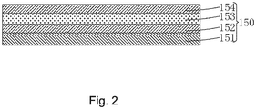
- the quantum dot layer light emitting chip 150 comprises a blue light emitting chip 151, a first insulation layer 152, a quantum dot layer 153, and a second insulation layer 154, which are provided on the bottom bracket 110 from bottom to top in order.
- the quantum dot layer 153 comprises two quantum dot materials, which respectively are a red quantum dot material and a green quantum dot material; the top silica gel layer 190 is a transparent silica gel material.
- the quantum dot layer 153 comprises only a green quantum dot material; and the top silica gel layer 190 is a silica gel layer comprising a KSF phosphorescent material, and such kind of quantum dot LED package structure has higher luminous efficiency because the KSF phosphorescent material does not absorb the green light wave band.
- a material of the first insulation layer 152 and the second insulation layer 154 is silica gel or glass.
- the bottom bracket 110 comprises a first metal bracket 111 and a second metal bracket 112 spaced apart from each other, and an insulation bracket 113 positioned between the first metal bracket 111 and the second metal bracket 112; the first metal bracket 111 and the second metal bracket 112 are respectively connected with an electrode positive and a negative electrode of the blue light emitting chip 151.
- a material of the external bracket 130 and the insulation bracket 113 is an epoxy molding compound (EMC) or a ceramic.
- the blue light emitting chip 151 is a flip chip.
- the inorganic barrier layer 170 forms a recess above the quantum dot layer light emitting chip 150
- the top silica gel layer 190 is formed in the recess and is correspondingly above the quantum dot layer light emitting chip 150.
- the quantum dot LED package structure comprises a bottom bracket, an external bracket, a quantum dot layer light emitting chip, an inorganic barrier layer and a top silica gel layer, wherein the inorganic barrier layer covering the external bracket and the quantum dot layer light emitting chip on the bottom bracket to package the external bracket and the quantum dot layer light emitting chip; the external bracket and the quantum dot layer light emitting chip are packaged by using the inorganic barrier layer, and a top silica gel layer is provided on the inorganic barrier layer, and the water and oxygen barrier condition, that the existing package structure simply using the silica gel layer cannot meet, can be satisfied and good heat dissipation can be provided for the quantum dot LED.
- the issues of mass production difficulty, high cost, low luminous efficiency, difficulty to achieve narrow border application of the current quantum dot LED can be solved.
Landscapes
- Led Device Packages (AREA)
Abstract
Description
- The present invention relates to a display technology field, and more particularly to a quantum dot LED package structure.
- In recent years, the Thin Film Transistor-LCD (TFT-LCD) has been rapidly developed and applied widely. Most of the liquid crystal displays on the present market are back light type liquid crystal display devices, which comprise a liquid crystal display panel and a back light module. Generally, the liquid crystal display panel comprises a Color Filter (CF) substrate, a Thin Film Transistor (TFT) substrate, Liquid Crystal (LC) sandwiched between the CF substrate and TFT substrate and sealant. The working principle is that the light of backlight module is reflected to generate images by applying driving voltages to the two glass substrate for controlling the rotations of the liquid crystal molecules.
- In the liquid crystal display devices of prior art, the white light emitting diodes (Light Emitting Diode, LED) are generally used as a backlight. The most common white LED is a LED with the blue light emitting chip (B chip) plus yellow phosphor (Y phosphor). As the LEDs using the yellow phosphor is employed to be a backlight within a liquid crystal display panel, the display's color saturation is generally relatively lower (the NTSC color gamut value is generally 72%), the color is not bright enough. In order to improve the color saturation and to achieve more vivid color performance, the yellow phosphor is mainly changed to red green (RG) phosphor at present, for having the white LED with blue light emitting chip plus red green phosphor. However, compared to the yellow phosphor, such arrangement can only increase about 25% of the color gamut (the NTSC color gamut value is generally 90%), which still cannot meet the new BT.2020 color gamut standard (equivalent to the NTSC color gamut value of 134%). At present, the technology using the quantum dots (Quantum Dot, QD) material with a narrow emission spectrum is the technology, which is the easiest to implement and the most energy efficient technology within the technologies able to achieve 80% BT.2020 color gamut standard now.
- The quantum dots, also known as nanocrystals are nanoparticles, of which the particle sizes are generally between 1-10nm, and due to the quantum confinement of the electrons and the holes, the continuous band structure becomes a discrete level structure having a molecular characteristic, and can be excited to emit fluorescence. The emission spectrum of the quantum dots can be controlled by changing the size of the quantum dots. By changing the size of the quantum dots and the chemical composition thereof, the emission spectrum can cover the entire visible region, and includes a wide excitation spectrum and a narrow emission spectrum, and thus the spectral coverage rate is higher. Moreover, compared with the fluorescence lifetime of the organic phosphor, the fluorescence lifetime of quantum dots is 3-5 times to have a good light stability. In short, the quantum dots are an ideal fluorescent material.
- The quantum dot mixed material packaged in the LED bracket as a fluorescent luminescent material and silica gel is named as a quantum dot light emitting diode (QLED). However, the quantum dots are sensitive to water and oxygen, and the fluorescence efficiency will be irreversibly decreased as being exposed in the environment of water and oxygen. Therefore, the package of quantum dots needs to have a good water and oxygen insulation ability. In addition, as the temperature rise, the luminous efficiency of the quantum dot material will gradually decline, and the emission wavelength will be red shifted, so the quantum dot package needs to be able to insulate the high temperature or to have a better heat dissipation environment. At present, in the quantum dot LED backlight applications, the main package for the quantum dots is to package the quantum dots in the glass tube or in the water/oxygen-insulated polyethylene terephthalate (PET) film. However, the former uses the glass, and there are drawbacks of fragile, low light utilization, difficulty to achieve narrow border, while there are drawbacks of easily producing the blue light color shift of the backlight edge and high cost in the latter.
- An objective of the present invention is to provide a quantum dot LED package structure, possessing good heat dissipation effect and water oxygen barrier effect to solve the issues of mass production difficulty, high cost, low luminous efficiency, difficulty to achieve narrow border application of the current quantum dot LED.
- For realizing the aforesaid objective, the present invention provides a quantum dot LED package structure, comprising a bottom bracket, an external bracket, a quantum dot layer light emitting chip, an inorganic barrier layer and a top silica gel layer;
the quantum dot layer light emitting chip being provided on the bottom bracket;
the external bracket being provided on the bottom bracket and surrounding the quantum dot layer light emitting chip;
the inorganic barrier layer covering the external bracket and the quantum dot layer light emitting chip on the bottom bracket to package the external bracket and the quantum dot layer light emitting chip;
the top silica gel layer being provided on the inorganic barrier layer. - A material of the inorganic barrier layer is SiO2, AlN, SiAlN or Al2O3.
- The inorganic barrier layer is formed by a low temperature sputtering method, a plasma enhanced chemical vapor deposition method or a thermal evaporation method.
- The quantum dot layer light emitting chip comprises a blue light emitting chip, a first insulation layer, a quantum dot layer, and a second insulation layer, which are provided on the bottom bracket from bottom to top in order.
- The quantum dot layer comprises two quantum dot materials, which respectively are a red quantum dot material and a green quantum dot material.
- The quantum dot layer comprises a quantum dot material, which is a green quantum dot material;
the top silica gel layer is a silica gel layer comprising a KSF phosphorescent material. - A material of the first insulation layer and the second insulation layer is silica gel or glass.
- The bottom bracket comprises a first metal bracket and a second metal bracket spaced apart from each other, and an insulation bracket positioned between the first metal bracket and the second metal bracket;
the first metal bracket and the second metal bracket are respectively connected with an electrode positive and a negative electrode of the blue light emitting chip. - A material of the external bracket and the insulation bracket is an epoxy molding compound or a ceramic.
- The blue light emitting chip is a flip chip.
- The present invention further provides a quantum dot LED package structure, comprising a bottom bracket, an external bracket, a quantum dot layer light emitting chip, an inorganic barrier layer and a top silica gel layer;
the quantum dot layer light emitting chip being provided on the bottom bracket;
the external bracket being provided on the bottom bracket and surrounding the quantum dot layer light emitting chip;
the inorganic barrier layer covering the external bracket and the quantum dot layer light emitting chip on the bottom bracket to package the external bracket and the quantum dot layer light emitting chip;
the top silica gel layer being provided on the inorganic barrier layer;
wherein the inorganic barrier layer is formed by a low temperature sputtering method, a plasma enhanced chemical vapor deposition method or a thermal evaporation method;
wherein the quantum dot layer light emitting chip comprises a blue light emitting chip, a first insulation layer, a quantum dot layer, and a second insulation layer, which are provided on the bottom bracket from bottom to top in order. - The benefits of the present invention are: the present invention provides a quantum dot LED package structure comprising a bottom bracket, an external bracket, a quantum dot layer light emitting chip, an inorganic barrier layer and a top silica gel layer, wherein the inorganic barrier layer covering the external bracket and the quantum dot layer light emitting chip on the bottom bracket to package the external bracket and the quantum dot layer light emitting chip; the external bracket and the quantum dot layer light emitting chip are packaged by using the inorganic barrier layer, and a top silica gel layer is provided on the inorganic barrier layer, and the water and oxygen barrier condition, that the existing package structure simply using the silica gel layer cannot meet, can be satisfied and good heat dissipation can be provided for the quantum dot LED. Thus, the issues of mass production difficulty, high cost, low luminous efficiency, difficulty to achieve narrow border application of the current quantum dot LED can be solved.
- In order to better understand the characteristics and technical aspect of the invention, please refer to the following detailed description of the present invention is concerned with the diagrams, however, provide reference to the accompanying drawings and description only and is not intended to be limiting of the invention.
- The technical solution and the beneficial effects of the present invention are best understood from the following detailed description with reference to the accompanying figures and embodiments.
- In drawings,
-
FIG. 1 is a diagram of the quantum dot LED package structure according to the present invention; -
FIG. 2 is a structure diagram of the quantum dot LED package structure comprising a quantum dot layer light emitting chip according to the present invention. - For better explaining the technical solution and the effect of the present invention, the present invention will be further described in detail with the accompanying drawings and the specific embodiments.
- Please refer to
FIG. 1 . The present invention provides a quantum dot LED package structure, comprising a bottom bracket 110, anexternal bracket 130, a quantum dot layerlight emitting chip 150, aninorganic barrier layer 170 and a topsilica gel layer 190;
the quantum dot layerlight emitting chip 150 being provided on the bottom bracket 110;
theexternal bracket 130 being provided on the bottom bracket 110 and surrounding the quantum dot layerlight emitting chip 150;
theinorganic barrier layer 170 covering theexternal bracket 130 and the quantum dot layerlight emitting chip 150 on the bottom bracket 110 to package theexternal bracket 130 and the quantum dot layerlight emitting chip 150; - The top
silica gel layer 190 is provided on theinorganic barrier layer 170. Thus, the silica gel in the topsilica gel layer 190 may fill a portion of the defects of theinorganic barrier layer 170, which are formed on the surface in the deposition process to avoid the film cracking of the quantum dot LED package structure due to the rapid changes of the environmental temperature and the humidity in the usage. - The quantum dot LED package structure of the present invention packages the
external bracket 130 and the quantum dot layerlight emitting chip 150 by using theinorganic barrier layer 170 and provides a topsilica gel layer 190 on theinorganic barrier layer 170, and the water and oxygen barrier condition, that the existing package structure simply using the silica gel layer cannot meet, can be satisfied (generally, an oxygen permeability rate of the silica gel having a low water permeability and a low oxygen permeability is 120-350cc/m2.day, and the water and oxygen barrier condition that the quantum dot LED actually requires is oxygen permeability<10-1cc/m2.day) and good heat dissipation can be provided for the quantum dot LED. Thus, the issues of mass production difficulty, high cost, low luminous efficiency, difficulty to achieve narrow border application of the current quantum dot LED can be solved. - In particular, the
inorganic barrier layer 170 is an inorganic barrier material having a low water permeability and a low oxygen permeability. It cannot only improve the good heat dissipation of the quantum dot LED package structure but also can greatly improve the water oxygen barrier effect of the quantum dot LED package structure. Furthermore, a material of theinorganic barrier layer 170 can be silicon oxide (SiO2), aluminum nitride (AlN), silicon aluminum nitride (SiAlN), or aluminum oxide (Al2O3). - Specifically, the
inorganic barrier layer 170 is formed by a low temperature sputtering method, a plasma enhanced chemical vapor deposition method or a thermal evaporation method. - Specifically, as shown in
FIG. 2 , the quantum dot layerlight emitting chip 150 comprises a bluelight emitting chip 151, a first insulation layer 152, a quantum dot layer 153, and asecond insulation layer 154, which are provided on the bottom bracket 110 from bottom to top in order. - Selectably, the quantum dot layer 153 comprises two quantum dot materials, which respectively are a red quantum dot material and a green quantum dot material; the top
silica gel layer 190 is a transparent silica gel material. - Or, the quantum dot layer 153 comprises only a green quantum dot material; and the top
silica gel layer 190 is a silica gel layer comprising a KSF phosphorescent material, and such kind of quantum dot LED package structure has higher luminous efficiency because the KSF phosphorescent material does not absorb the green light wave band. - Specifically, a material of the first insulation layer 152 and the
second insulation layer 154 is silica gel or glass. - Specifically, the bottom bracket 110 comprises a first metal bracket 111 and a second metal bracket 112 spaced apart from each other, and an insulation bracket 113 positioned between the first metal bracket 111 and the second metal bracket 112; the first metal bracket 111 and the second metal bracket 112 are respectively connected with an electrode positive and a negative electrode of the blue
light emitting chip 151. - Specifically, a material of the
external bracket 130 and the insulation bracket 113 is an epoxy molding compound (EMC) or a ceramic. - Specifically, the blue
light emitting chip 151 is a flip chip. - Specifically, the
inorganic barrier layer 170 forms a recess above the quantum dot layerlight emitting chip 150, and the topsilica gel layer 190 is formed in the recess and is correspondingly above the quantum dot layerlight emitting chip 150. - In conclusion, the quantum dot LED package structure provided by the present invention comprises a bottom bracket, an external bracket, a quantum dot layer light emitting chip, an inorganic barrier layer and a top silica gel layer, wherein the inorganic barrier layer covering the external bracket and the quantum dot layer light emitting chip on the bottom bracket to package the external bracket and the quantum dot layer light emitting chip; the external bracket and the quantum dot layer light emitting chip are packaged by using the inorganic barrier layer, and a top silica gel layer is provided on the inorganic barrier layer, and the water and oxygen barrier condition, that the existing package structure simply using the silica gel layer cannot meet, can be satisfied and good heat dissipation can be provided for the quantum dot LED. Thus, the issues of mass production difficulty, high cost, low luminous efficiency, difficulty to achieve narrow border application of the current quantum dot LED can be solved.
- Above are only specific embodiments of the present invention, the scope of the present invention is not limited to this, and to any persons who are skilled in the art, change or replacement which is easily derived should be covered by the protected scope of the invention. Thus, the protected scope of the invention should go by the subject claims.
Claims (18)
- A quantum dot LED package structure, comprising a bottom bracket, an external bracket, a quantum dot layer light emitting chip, an inorganic barrier layer and a top silica gel layer;
the quantum dot layer light emitting chip being provided on the bottom bracket;
the external bracket being provided on the bottom bracket and surrounding the quantum dot layer light emitting chip;
the inorganic barrier layer covering the external bracket and the quantum dot layer light emitting chip on the bottom bracket to package the external bracket and the quantum dot layer light emitting chip;
the top silica gel layer being provided on the inorganic barrier layer. - The quantum dot LED package structure according to claim 1, wherein a material of the inorganic barrier layer is SiO2, AlN, SiAlN or Al2O3.
- The quantum dot LED package structure according to claim 1, wherein the inorganic barrier layer is formed by a low temperature sputtering method, a plasma enhanced chemical vapor deposition method or a thermal evaporation method.
- The quantum dot LED package structure according to claim 1, wherein the quantum dot layer light emitting chip comprises a blue light emitting chip, a first insulation layer, a quantum dot layer, and a second insulation layer, which are provided on the bottom bracket from bottom to top in order.
- The quantum dot LED package structure according to claim 4, wherein the quantum dot layer comprises two quantum dot materials, which respectively are a red quantum dot material and a green quantum dot material.
- The quantum dot LED package structure according to claim 4, wherein the quantum dot layer comprises a quantum dot material, which is a green quantum dot material;
the top silica gel layer is a silica gel layer comprising a KSF phosphorescent material. - The quantum dot LED package structure according to claim 4, wherein a material of the first insulation layer and the second insulation layer is silica gel or glass.
- The quantum dot LED package structure according to claim 4, wherein the bottom bracket comprises a first metal bracket and a second metal bracket spaced apart from each other, and an insulation bracket positioned between the first metal bracket and the second metal bracket;
the first metal bracket and the second metal bracket are respectively connected with an electrode positive and a negative electrode of the blue light emitting chip. - The quantum dot LED package structure according to claim 8, wherein a material of the external bracket and the insulation bracket is an epoxy molding compound or a ceramic.
- The quantum dot LED package structure according to claim 4, wherein the blue light emitting chip is a flip chip.
- A quantum dot LED package structure, comprising a bottom bracket, an external bracket, a quantum dot layer light emitting chip, an inorganic barrier layer and a top silica gel layer;
the quantum dot layer light emitting chip being provided on the bottom bracket;
the external bracket being provided on the bottom bracket and surrounding the quantum dot layer light emitting chip;
the inorganic barrier layer covering the external bracket and the quantum dot layer light emitting chip on the bottom bracket to package the external bracket and the quantum dot layer light emitting chip;
the top silica gel layer being provided on the inorganic barrier layer;
wherein the inorganic barrier layer is formed by a low temperature sputtering method, a plasma enhanced chemical vapor deposition method or a thermal evaporation method;
wherein the quantum dot layer light emitting chip comprises a blue light emitting chip, a first insulation layer, a quantum dot layer, and a second insulation layer, which are provided on the bottom bracket from bottom to top in order. - The quantum dot LED package structure according to claim 11, wherein a material of the inorganic barrier layer is SiO2, AlN, SiAlN or Al2O3.
- The quantum dot LED package structure according to claim 11, wherein the quantum dot layer comprises two quantum dot materials, which respectively are a red quantum dot material and a green quantum dot material.
- The quantum dot LED package structure according to claim 11, wherein the quantum dot layer comprises a quantum dot material, which is a green quantum dot material;
the top silica gel layer is a silica gel layer comprising a KSF phosphorescent material. - The quantum dot LED package structure according to claim 11, wherein a material of the first insulation layer and the second insulation layer is silica gel or glass.
- The quantum dot LED package structure according to claim 11, wherein the bottom bracket comprises a first metal bracket and a second metal bracket spaced apart from each other, and an insulation bracket positioned between the first metal bracket and the second metal bracket;
the first metal bracket and the second metal bracket are respectively connected with an electrode positive and a negative electrode of the blue light emitting chip. - The quantum dot LED package structure according to claim 16, wherein a material of the external bracket and the insulation bracket is an epoxy molding compound or a ceramic.
- The quantum dot LED package structure according to claim 11, wherein the blue light emitting chip is a flip chip.
Applications Claiming Priority (2)
| Application Number | Priority Date | Filing Date | Title |
|---|---|---|---|
| CN201710202967.1A CN106981562B (en) | 2017-03-30 | 2017-03-30 | Quantum dot LED encapsulation structure |
| PCT/CN2017/081034 WO2018176525A1 (en) | 2017-03-30 | 2017-04-19 | Quantum dot led packaging structure |
Publications (3)
| Publication Number | Publication Date |
|---|---|
| EP3605621A1 true EP3605621A1 (en) | 2020-02-05 |
| EP3605621A4 EP3605621A4 (en) | 2020-12-16 |
| EP3605621B1 EP3605621B1 (en) | 2022-03-23 |
Family
ID=59339285
Family Applications (1)
| Application Number | Title | Priority Date | Filing Date |
|---|---|---|---|
| EP17903598.5A Active EP3605621B1 (en) | 2017-03-30 | 2017-04-19 | Quantum dot led packaging structure |
Country Status (7)
| Country | Link |
|---|---|
| US (1) | US10134962B2 (en) |
| EP (1) | EP3605621B1 (en) |
| JP (1) | JP6852250B2 (en) |
| KR (1) | KR20190127932A (en) |
| CN (1) | CN106981562B (en) |
| PL (1) | PL3605621T3 (en) |
| WO (1) | WO2018176525A1 (en) |
Families Citing this family (16)
| Publication number | Priority date | Publication date | Assignee | Title |
|---|---|---|---|---|
| CN206741157U (en) * | 2017-04-19 | 2017-12-12 | 深圳Tcl新技术有限公司 | LED lamp source, lamp bar and display device |
| CN107565003B (en) * | 2017-07-31 | 2019-04-30 | 深圳市华星光电技术有限公司 | Quantum dot LED encapsulation structure |
| CN107833963A (en) * | 2017-09-21 | 2018-03-23 | 华南师范大学 | The secondary airtight packaging method of quantum dot On chip white light LEDs |
| CN108011020B (en) * | 2018-01-12 | 2020-02-07 | 惠州市华星光电技术有限公司 | Quantum dot diaphragm and backlight module |
| CN108281530A (en) * | 2018-01-31 | 2018-07-13 | 惠州市华星光电技术有限公司 | A kind of quantum dot LED, backlight module and display device |
| CN108493319A (en) * | 2018-03-21 | 2018-09-04 | 惠州市华星光电技术有限公司 | A kind of light emitting diode with quantum dots light source and light emitting diode |
| CN108400223A (en) * | 2018-05-07 | 2018-08-14 | 深圳技术大学(筹) | Light-emitting diode encapsulation structure, quantum dot sealing unit and preparation method thereof |
| CN108735879A (en) * | 2018-07-26 | 2018-11-02 | 易美芯光(北京)科技有限公司 | A kind of SMD encapsulating structures containing quantum dot |
| KR20200049929A (en) * | 2018-10-29 | 2020-05-11 | 삼성디스플레이 주식회사 | Optical member and display divice including the same |
| CN110212074B (en) * | 2019-06-03 | 2020-04-28 | 李红云 | Quantum dot light-emitting diode packaging structure containing optical improvement layer |
| US11099424B2 (en) | 2019-07-02 | 2021-08-24 | Dell Products L.P. | High color gamut LED bar with side illumination LED package |
| CN111403578B (en) * | 2020-03-17 | 2021-04-06 | 深圳深旨科技有限公司 | Method for packaging deep ultraviolet LED chip by magnetron sputtering |
| CN111725422A (en) * | 2020-06-09 | 2020-09-29 | 武汉华星光电半导体显示技术有限公司 | Display panel, preparation method thereof and display device |
| CN114361316B (en) * | 2022-01-05 | 2025-10-03 | 深圳市朋威科技有限公司 | A method for preparing quantum dot LED lamp beads |
| JP7685454B2 (en) * | 2022-02-25 | 2025-05-29 | 日本特殊陶業株式会社 | Wavelength conversion member, its manufacturing method, and light emitting device |
| KR102880254B1 (en) * | 2025-04-24 | 2025-11-04 | 주식회사 동부엘이디 | LED package manufacturing method and LED package manufactured by the same |
Family Cites Families (20)
| Publication number | Priority date | Publication date | Assignee | Title |
|---|---|---|---|---|
| JP4727297B2 (en) * | 2005-05-19 | 2011-07-20 | 三菱電機株式会社 | Semiconductor light emitting device |
| JP2007123390A (en) * | 2005-10-26 | 2007-05-17 | Kyocera Corp | Light emitting device |
| KR101592836B1 (en) * | 2008-02-07 | 2016-02-05 | 미쓰비시 가가꾸 가부시키가이샤 | Semiconductor light emitting device, backlighting device, color image display device and phosphor used for those devices |
| GB0916700D0 (en) * | 2009-09-23 | 2009-11-04 | Nanoco Technologies Ltd | Semiconductor nanoparticle-based materials |
| JP2011204986A (en) * | 2010-03-26 | 2011-10-13 | Showa Denko Kk | Lamp and method for manufacturing the same |
| WO2012132236A1 (en) * | 2011-03-31 | 2012-10-04 | パナソニック株式会社 | Semiconductor light-emitting element and light-emitting device |
| US9443998B2 (en) * | 2013-03-14 | 2016-09-13 | Nanoco Technologies Ltd. | Multi-layer-coated quantum dot beads |
| KR101539206B1 (en) * | 2013-04-30 | 2015-07-23 | 소코 가가쿠 가부시키가이샤 | Ultraviolet light-emitting device |
| JP6232792B2 (en) * | 2013-07-17 | 2017-11-22 | 日亜化学工業株式会社 | Light emitting device |
| CN103681990B (en) * | 2013-12-11 | 2017-09-01 | 深圳市华星光电技术有限公司 | LED encapsulation piece and preparation method thereof |
| CN203850332U (en) * | 2013-12-19 | 2014-09-24 | 易美芯光(北京)科技有限公司 | Novel LED packaging structure |
| KR20150092801A (en) * | 2014-02-05 | 2015-08-17 | 삼성디스플레이 주식회사 | Light Emitting Diode Package and Method of manufacturing the same |
| KR102098245B1 (en) * | 2014-02-11 | 2020-04-07 | 삼성전자 주식회사 | Light source package and a display device including the same |
| CN104167426B (en) * | 2014-06-03 | 2017-08-01 | 上海天马有机发光显示技术有限公司 | A kind of organic LED display panel and preparation method thereof and display device |
| US9620686B2 (en) * | 2015-01-28 | 2017-04-11 | Apple Inc. | Display light sources with quantum dots |
| CN106299076B (en) * | 2015-05-19 | 2019-02-01 | 青岛海信电器股份有限公司 | A quantum dot light-emitting element, backlight module and display device |
| CN105185890A (en) * | 2015-08-10 | 2015-12-23 | 深圳市华星光电技术有限公司 | LED light source structure and packaging method thereof |
| CN205452347U (en) * | 2015-09-29 | 2016-08-10 | 易美芯光(北京)科技有限公司 | Support type quantum dot LED packaging structure |
| CN105867026A (en) * | 2016-06-03 | 2016-08-17 | 青岛海信电器股份有限公司 | Quantum dot light source device, backlight module and liquid crystal display device |
| US10203547B2 (en) * | 2016-06-16 | 2019-02-12 | Hisense Electric Co., Ltd. | Quantum dot light emitting device, backlight module, and liquid crystal display device |
-
2017
- 2017-03-30 CN CN201710202967.1A patent/CN106981562B/en active Active
- 2017-04-19 JP JP2019553554A patent/JP6852250B2/en active Active
- 2017-04-19 EP EP17903598.5A patent/EP3605621B1/en active Active
- 2017-04-19 KR KR1020197031577A patent/KR20190127932A/en not_active Ceased
- 2017-04-19 PL PL17903598.5T patent/PL3605621T3/en unknown
- 2017-04-19 US US15/529,507 patent/US10134962B2/en active Active
- 2017-04-19 WO PCT/CN2017/081034 patent/WO2018176525A1/en not_active Ceased
Also Published As
| Publication number | Publication date |
|---|---|
| KR20190127932A (en) | 2019-11-13 |
| EP3605621A4 (en) | 2020-12-16 |
| WO2018176525A1 (en) | 2018-10-04 |
| EP3605621B1 (en) | 2022-03-23 |
| JP6852250B2 (en) | 2021-03-31 |
| CN106981562B (en) | 2019-04-02 |
| JP2020512704A (en) | 2020-04-23 |
| PL3605621T3 (en) | 2022-08-01 |
| US10134962B2 (en) | 2018-11-20 |
| US20180309032A1 (en) | 2018-10-25 |
| CN106981562A (en) | 2017-07-25 |
Similar Documents
| Publication | Publication Date | Title |
|---|---|---|
| US10134962B2 (en) | Quantum dot LED package structure | |
| TWI604239B (en) | Color conversion substrate, method of fabricating the same, and display device including the same | |
| JP4767243B2 (en) | White light source, backlight unit and LCD display | |
| CN107565003B (en) | Quantum dot LED encapsulation structure | |
| CN106094328B (en) | Light conversion panel and light emitting diode package, backlight unit and display device including the same | |
| US20110037926A1 (en) | Light emitting device, display device, and color conversion sheet | |
| TW202009580A (en) | Pixel array package structure and display panel | |
| KR102474116B1 (en) | Display device | |
| TWI547208B (en) | Organic electroluminescent apparatus | |
| WO2019140707A1 (en) | White-light led, and preparation method therefor and use thereof | |
| CN107728369A (en) | Display panel and manufacturing method thereof | |
| US20120014091A1 (en) | Led package assembly and backlight module | |
| WO2020177187A1 (en) | Display panel and display module | |
| US20170139092A1 (en) | Polarizer, Quantum-Effect-Based Display Panel and Display Device | |
| CN107741664A (en) | Display panel and manufacturing method thereof | |
| WO2019085173A1 (en) | Liquid crystal display | |
| US9893248B2 (en) | Substrate for changing color of light emitting diode and method for producing same | |
| CN101840987A (en) | White light emitting device and white light source module using the white light emitting device | |
| CN106716653A (en) | Substrate for color conversion of light-emitting diode and manufacturing method therefor | |
| TW201543713A (en) | Color conversion substrate for light emitting diode and manufacturing method thereof | |
| Kim et al. | Optimal design of a quantum dot color conversion film in LCD backlighting | |
| JP6743630B2 (en) | Light emitting device and manufacturing method thereof | |
| KR101806870B1 (en) | Light guide panel patterned color converting phosphor layer, display device and display panel comprising the same | |
| KR101942253B1 (en) | Phosphor and light emitting diode having the same | |
| CN111081847A (en) | Light Emitting Diodes and Light Source Devices |
Legal Events
| Date | Code | Title | Description |
|---|---|---|---|
| STAA | Information on the status of an ep patent application or granted ep patent |
Free format text: STATUS: THE INTERNATIONAL PUBLICATION HAS BEEN MADE |
|
| PUAI | Public reference made under article 153(3) epc to a published international application that has entered the european phase |
Free format text: ORIGINAL CODE: 0009012 |
|
| STAA | Information on the status of an ep patent application or granted ep patent |
Free format text: STATUS: REQUEST FOR EXAMINATION WAS MADE |
|
| 17P | Request for examination filed |
Effective date: 20191030 |
|
| AK | Designated contracting states |
Kind code of ref document: A1 Designated state(s): AL AT BE BG CH CY CZ DE DK EE ES FI FR GB GR HR HU IE IS IT LI LT LU LV MC MK MT NL NO PL PT RO RS SE SI SK SM TR |
|
| AX | Request for extension of the european patent |
Extension state: BA ME |
|
| DAV | Request for validation of the european patent (deleted) | ||
| DAX | Request for extension of the european patent (deleted) | ||
| A4 | Supplementary search report drawn up and despatched |
Effective date: 20201112 |
|
| RIC1 | Information provided on ipc code assigned before grant |
Ipc: H01L 33/50 20100101ALI20201106BHEP Ipc: H01L 33/64 20100101ALI20201106BHEP Ipc: H01L 33/56 20100101AFI20201106BHEP Ipc: H01L 33/44 20100101ALI20201106BHEP Ipc: H01L 33/54 20100101ALI20201106BHEP |
|
| GRAP | Despatch of communication of intention to grant a patent |
Free format text: ORIGINAL CODE: EPIDOSNIGR1 |
|
| STAA | Information on the status of an ep patent application or granted ep patent |
Free format text: STATUS: GRANT OF PATENT IS INTENDED |
|
| RIC1 | Information provided on ipc code assigned before grant |
Ipc: H01L 33/44 20100101ALI20211021BHEP Ipc: H01L 33/50 20100101ALI20211021BHEP Ipc: H01L 33/64 20100101ALI20211021BHEP Ipc: H01L 33/54 20100101ALI20211021BHEP Ipc: H01L 33/56 20100101AFI20211021BHEP |
|
| INTG | Intention to grant announced |
Effective date: 20211115 |
|
| GRAS | Grant fee paid |
Free format text: ORIGINAL CODE: EPIDOSNIGR3 |
|
| GRAA | (expected) grant |
Free format text: ORIGINAL CODE: 0009210 |
|
| STAA | Information on the status of an ep patent application or granted ep patent |
Free format text: STATUS: THE PATENT HAS BEEN GRANTED |
|
| AK | Designated contracting states |
Kind code of ref document: B1 Designated state(s): AL AT BE BG CH CY CZ DE DK EE ES FI FR GB GR HR HU IE IS IT LI LT LU LV MC MK MT NL NO PL PT RO RS SE SI SK SM TR |
|
| RAP3 | Party data changed (applicant data changed or rights of an application transferred) |
Owner name: SHENZHEN CHINA STAR OPTOELECTRONICS TECHNOLOGY CO., LTD. |
|
| REG | Reference to a national code |
Ref country code: GB Ref legal event code: FG4D |
|
| REG | Reference to a national code |
Ref country code: CH Ref legal event code: EP |
|
| REG | Reference to a national code |
Ref country code: DE Ref legal event code: R096 Ref document number: 602017055081 Country of ref document: DE |
|
| REG | Reference to a national code |
Ref country code: IE Ref legal event code: FG4D |
|
| REG | Reference to a national code |
Ref country code: AT Ref legal event code: REF Ref document number: 1478054 Country of ref document: AT Kind code of ref document: T Effective date: 20220415 |
|
| REG | Reference to a national code |
Ref country code: LT Ref legal event code: MG9D |
|
| REG | Reference to a national code |
Ref country code: NL Ref legal event code: MP Effective date: 20220323 |
|
| PG25 | Lapsed in a contracting state [announced via postgrant information from national office to epo] |
Ref country code: SE Free format text: LAPSE BECAUSE OF FAILURE TO SUBMIT A TRANSLATION OF THE DESCRIPTION OR TO PAY THE FEE WITHIN THE PRESCRIBED TIME-LIMIT Effective date: 20220323 Ref country code: RS Free format text: LAPSE BECAUSE OF FAILURE TO SUBMIT A TRANSLATION OF THE DESCRIPTION OR TO PAY THE FEE WITHIN THE PRESCRIBED TIME-LIMIT Effective date: 20220323 Ref country code: NO Free format text: LAPSE BECAUSE OF FAILURE TO SUBMIT A TRANSLATION OF THE DESCRIPTION OR TO PAY THE FEE WITHIN THE PRESCRIBED TIME-LIMIT Effective date: 20220623 Ref country code: LT Free format text: LAPSE BECAUSE OF FAILURE TO SUBMIT A TRANSLATION OF THE DESCRIPTION OR TO PAY THE FEE WITHIN THE PRESCRIBED TIME-LIMIT Effective date: 20220323 Ref country code: HR Free format text: LAPSE BECAUSE OF FAILURE TO SUBMIT A TRANSLATION OF THE DESCRIPTION OR TO PAY THE FEE WITHIN THE PRESCRIBED TIME-LIMIT Effective date: 20220323 Ref country code: BG Free format text: LAPSE BECAUSE OF FAILURE TO SUBMIT A TRANSLATION OF THE DESCRIPTION OR TO PAY THE FEE WITHIN THE PRESCRIBED TIME-LIMIT Effective date: 20220623 |
|
| REG | Reference to a national code |
Ref country code: AT Ref legal event code: MK05 Ref document number: 1478054 Country of ref document: AT Kind code of ref document: T Effective date: 20220323 |
|
| PG25 | Lapsed in a contracting state [announced via postgrant information from national office to epo] |
Ref country code: LV Free format text: LAPSE BECAUSE OF FAILURE TO SUBMIT A TRANSLATION OF THE DESCRIPTION OR TO PAY THE FEE WITHIN THE PRESCRIBED TIME-LIMIT Effective date: 20220323 Ref country code: GR Free format text: LAPSE BECAUSE OF FAILURE TO SUBMIT A TRANSLATION OF THE DESCRIPTION OR TO PAY THE FEE WITHIN THE PRESCRIBED TIME-LIMIT Effective date: 20220624 Ref country code: FI Free format text: LAPSE BECAUSE OF FAILURE TO SUBMIT A TRANSLATION OF THE DESCRIPTION OR TO PAY THE FEE WITHIN THE PRESCRIBED TIME-LIMIT Effective date: 20220323 |
|
| PG25 | Lapsed in a contracting state [announced via postgrant information from national office to epo] |
Ref country code: NL Free format text: LAPSE BECAUSE OF FAILURE TO SUBMIT A TRANSLATION OF THE DESCRIPTION OR TO PAY THE FEE WITHIN THE PRESCRIBED TIME-LIMIT Effective date: 20220323 |
|
| PG25 | Lapsed in a contracting state [announced via postgrant information from national office to epo] |
Ref country code: SM Free format text: LAPSE BECAUSE OF FAILURE TO SUBMIT A TRANSLATION OF THE DESCRIPTION OR TO PAY THE FEE WITHIN THE PRESCRIBED TIME-LIMIT Effective date: 20220323 Ref country code: SK Free format text: LAPSE BECAUSE OF FAILURE TO SUBMIT A TRANSLATION OF THE DESCRIPTION OR TO PAY THE FEE WITHIN THE PRESCRIBED TIME-LIMIT Effective date: 20220323 Ref country code: RO Free format text: LAPSE BECAUSE OF FAILURE TO SUBMIT A TRANSLATION OF THE DESCRIPTION OR TO PAY THE FEE WITHIN THE PRESCRIBED TIME-LIMIT Effective date: 20220323 Ref country code: PT Free format text: LAPSE BECAUSE OF FAILURE TO SUBMIT A TRANSLATION OF THE DESCRIPTION OR TO PAY THE FEE WITHIN THE PRESCRIBED TIME-LIMIT Effective date: 20220725 Ref country code: ES Free format text: LAPSE BECAUSE OF FAILURE TO SUBMIT A TRANSLATION OF THE DESCRIPTION OR TO PAY THE FEE WITHIN THE PRESCRIBED TIME-LIMIT Effective date: 20220323 Ref country code: EE Free format text: LAPSE BECAUSE OF FAILURE TO SUBMIT A TRANSLATION OF THE DESCRIPTION OR TO PAY THE FEE WITHIN THE PRESCRIBED TIME-LIMIT Effective date: 20220323 Ref country code: CZ Free format text: LAPSE BECAUSE OF FAILURE TO SUBMIT A TRANSLATION OF THE DESCRIPTION OR TO PAY THE FEE WITHIN THE PRESCRIBED TIME-LIMIT Effective date: 20220323 Ref country code: AT Free format text: LAPSE BECAUSE OF FAILURE TO SUBMIT A TRANSLATION OF THE DESCRIPTION OR TO PAY THE FEE WITHIN THE PRESCRIBED TIME-LIMIT Effective date: 20220323 |
|
| PG25 | Lapsed in a contracting state [announced via postgrant information from national office to epo] |
Ref country code: IS Free format text: LAPSE BECAUSE OF FAILURE TO SUBMIT A TRANSLATION OF THE DESCRIPTION OR TO PAY THE FEE WITHIN THE PRESCRIBED TIME-LIMIT Effective date: 20220723 Ref country code: AL Free format text: LAPSE BECAUSE OF FAILURE TO SUBMIT A TRANSLATION OF THE DESCRIPTION OR TO PAY THE FEE WITHIN THE PRESCRIBED TIME-LIMIT Effective date: 20220323 |
|
| REG | Reference to a national code |
Ref country code: CH Ref legal event code: PL |
|
| REG | Reference to a national code |
Ref country code: DE Ref legal event code: R097 Ref document number: 602017055081 Country of ref document: DE |
|
| REG | Reference to a national code |
Ref country code: BE Ref legal event code: MM Effective date: 20220430 |
|
| PLBE | No opposition filed within time limit |
Free format text: ORIGINAL CODE: 0009261 |
|
| STAA | Information on the status of an ep patent application or granted ep patent |
Free format text: STATUS: NO OPPOSITION FILED WITHIN TIME LIMIT |
|
| PG25 | Lapsed in a contracting state [announced via postgrant information from national office to epo] |
Ref country code: MC Free format text: LAPSE BECAUSE OF FAILURE TO SUBMIT A TRANSLATION OF THE DESCRIPTION OR TO PAY THE FEE WITHIN THE PRESCRIBED TIME-LIMIT Effective date: 20220323 Ref country code: LU Free format text: LAPSE BECAUSE OF NON-PAYMENT OF DUE FEES Effective date: 20220419 Ref country code: LI Free format text: LAPSE BECAUSE OF NON-PAYMENT OF DUE FEES Effective date: 20220430 Ref country code: DK Free format text: LAPSE BECAUSE OF FAILURE TO SUBMIT A TRANSLATION OF THE DESCRIPTION OR TO PAY THE FEE WITHIN THE PRESCRIBED TIME-LIMIT Effective date: 20220323 Ref country code: CH Free format text: LAPSE BECAUSE OF NON-PAYMENT OF DUE FEES Effective date: 20220430 |
|
| PG25 | Lapsed in a contracting state [announced via postgrant information from national office to epo] |
Ref country code: BE Free format text: LAPSE BECAUSE OF NON-PAYMENT OF DUE FEES Effective date: 20220430 |
|
| 26N | No opposition filed |
Effective date: 20230102 |
|
| PG25 | Lapsed in a contracting state [announced via postgrant information from national office to epo] |
Ref country code: IE Free format text: LAPSE BECAUSE OF NON-PAYMENT OF DUE FEES Effective date: 20220419 |
|
| PG25 | Lapsed in a contracting state [announced via postgrant information from national office to epo] |
Ref country code: SI Free format text: LAPSE BECAUSE OF FAILURE TO SUBMIT A TRANSLATION OF THE DESCRIPTION OR TO PAY THE FEE WITHIN THE PRESCRIBED TIME-LIMIT Effective date: 20220323 |
|
| P01 | Opt-out of the competence of the unified patent court (upc) registered |
Effective date: 20230530 |
|
| PG25 | Lapsed in a contracting state [announced via postgrant information from national office to epo] |
Ref country code: IT Free format text: LAPSE BECAUSE OF FAILURE TO SUBMIT A TRANSLATION OF THE DESCRIPTION OR TO PAY THE FEE WITHIN THE PRESCRIBED TIME-LIMIT Effective date: 20220323 |
|
| PG25 | Lapsed in a contracting state [announced via postgrant information from national office to epo] |
Ref country code: MK Free format text: LAPSE BECAUSE OF FAILURE TO SUBMIT A TRANSLATION OF THE DESCRIPTION OR TO PAY THE FEE WITHIN THE PRESCRIBED TIME-LIMIT Effective date: 20220323 Ref country code: CY Free format text: LAPSE BECAUSE OF FAILURE TO SUBMIT A TRANSLATION OF THE DESCRIPTION OR TO PAY THE FEE WITHIN THE PRESCRIBED TIME-LIMIT Effective date: 20220323 |
|
| PG25 | Lapsed in a contracting state [announced via postgrant information from national office to epo] |
Ref country code: HU Free format text: LAPSE BECAUSE OF FAILURE TO SUBMIT A TRANSLATION OF THE DESCRIPTION OR TO PAY THE FEE WITHIN THE PRESCRIBED TIME-LIMIT; INVALID AB INITIO Effective date: 20170419 |
|
| PG25 | Lapsed in a contracting state [announced via postgrant information from national office to epo] |
Ref country code: TR Free format text: LAPSE BECAUSE OF FAILURE TO SUBMIT A TRANSLATION OF THE DESCRIPTION OR TO PAY THE FEE WITHIN THE PRESCRIBED TIME-LIMIT Effective date: 20220323 |
|
| PG25 | Lapsed in a contracting state [announced via postgrant information from national office to epo] |
Ref country code: MT Free format text: LAPSE BECAUSE OF FAILURE TO SUBMIT A TRANSLATION OF THE DESCRIPTION OR TO PAY THE FEE WITHIN THE PRESCRIBED TIME-LIMIT Effective date: 20220323 |
|
| REG | Reference to a national code |
Ref country code: DE Ref legal event code: R079 Ref document number: 602017055081 Country of ref document: DE Free format text: PREVIOUS MAIN CLASS: H01L0033560000 Ipc: H10H0020854000 |
|
| PGFP | Annual fee paid to national office [announced via postgrant information from national office to epo] |
Ref country code: PL Payment date: 20250411 Year of fee payment: 9 Ref country code: DE Payment date: 20250422 Year of fee payment: 9 |
|
| PGFP | Annual fee paid to national office [announced via postgrant information from national office to epo] |
Ref country code: GB Payment date: 20250423 Year of fee payment: 9 |
|
| PGFP | Annual fee paid to national office [announced via postgrant information from national office to epo] |
Ref country code: FR Payment date: 20250425 Year of fee payment: 9 |