EP3602188B1 - Vorrichtung zur thz-erzeugung und/oder -detektion und verfahren zur herstellung davon - Google Patents
Vorrichtung zur thz-erzeugung und/oder -detektion und verfahren zur herstellung davon Download PDFInfo
- Publication number
- EP3602188B1 EP3602188B1 EP18712572.9A EP18712572A EP3602188B1 EP 3602188 B1 EP3602188 B1 EP 3602188B1 EP 18712572 A EP18712572 A EP 18712572A EP 3602188 B1 EP3602188 B1 EP 3602188B1
- Authority
- EP
- European Patent Office
- Prior art keywords
- waveguide
- terahertz
- nonlinear
- cladding
- optical
- Prior art date
- Legal status (The legal status is an assumption and is not a legal conclusion. Google has not performed a legal analysis and makes no representation as to the accuracy of the status listed.)
- Active
Links
Images


Classifications
-
- G—PHYSICS
- G01—MEASURING; TESTING
- G01N—INVESTIGATING OR ANALYSING MATERIALS BY DETERMINING THEIR CHEMICAL OR PHYSICAL PROPERTIES
- G01N21/00—Investigating or analysing materials by the use of optical means, i.e. using sub-millimetre waves, infrared, visible or ultraviolet light
- G01N21/17—Systems in which incident light is modified in accordance with the properties of the material investigated
- G01N21/25—Colour; Spectral properties, i.e. comparison of effect of material on the light at two or more different wavelengths or wavelength bands
- G01N21/31—Investigating relative effect of material at wavelengths characteristic of specific elements or molecules, e.g. atomic absorption spectrometry
- G01N21/35—Investigating relative effect of material at wavelengths characteristic of specific elements or molecules, e.g. atomic absorption spectrometry using infrared light
- G01N21/3581—Investigating relative effect of material at wavelengths characteristic of specific elements or molecules, e.g. atomic absorption spectrometry using infrared light using far infrared light; using Terahertz radiation
- G01N21/3586—Investigating relative effect of material at wavelengths characteristic of specific elements or molecules, e.g. atomic absorption spectrometry using infrared light using far infrared light; using Terahertz radiation by Terahertz time domain spectroscopy [THz-TDS]
-
- G—PHYSICS
- G02—OPTICS
- G02F—OPTICAL DEVICES OR ARRANGEMENTS FOR THE CONTROL OF LIGHT BY MODIFICATION OF THE OPTICAL PROPERTIES OF THE MEDIA OF THE ELEMENTS INVOLVED THEREIN; NON-LINEAR OPTICS; FREQUENCY-CHANGING OF LIGHT; OPTICAL LOGIC ELEMENTS; OPTICAL ANALOGUE/DIGITAL CONVERTERS
- G02F1/00—Devices or arrangements for the control of the intensity, colour, phase, polarisation or direction of light arriving from an independent light source, e.g. switching, gating or modulating; Non-linear optics
- G02F1/01—Devices or arrangements for the control of the intensity, colour, phase, polarisation or direction of light arriving from an independent light source, e.g. switching, gating or modulating; Non-linear optics for the control of the intensity, phase, polarisation or colour
- G02F1/03—Devices or arrangements for the control of the intensity, colour, phase, polarisation or direction of light arriving from an independent light source, e.g. switching, gating or modulating; Non-linear optics for the control of the intensity, phase, polarisation or colour based on ceramics or electro-optical crystals, e.g. exhibiting Pockels effect or Kerr effect
- G02F1/05—Devices or arrangements for the control of the intensity, colour, phase, polarisation or direction of light arriving from an independent light source, e.g. switching, gating or modulating; Non-linear optics for the control of the intensity, phase, polarisation or colour based on ceramics or electro-optical crystals, e.g. exhibiting Pockels effect or Kerr effect with ferro-electric properties
-
- G—PHYSICS
- G02—OPTICS
- G02F—OPTICAL DEVICES OR ARRANGEMENTS FOR THE CONTROL OF LIGHT BY MODIFICATION OF THE OPTICAL PROPERTIES OF THE MEDIA OF THE ELEMENTS INVOLVED THEREIN; NON-LINEAR OPTICS; FREQUENCY-CHANGING OF LIGHT; OPTICAL LOGIC ELEMENTS; OPTICAL ANALOGUE/DIGITAL CONVERTERS
- G02F1/00—Devices or arrangements for the control of the intensity, colour, phase, polarisation or direction of light arriving from an independent light source, e.g. switching, gating or modulating; Non-linear optics
- G02F1/01—Devices or arrangements for the control of the intensity, colour, phase, polarisation or direction of light arriving from an independent light source, e.g. switching, gating or modulating; Non-linear optics for the control of the intensity, phase, polarisation or colour
- G02F1/03—Devices or arrangements for the control of the intensity, colour, phase, polarisation or direction of light arriving from an independent light source, e.g. switching, gating or modulating; Non-linear optics for the control of the intensity, phase, polarisation or colour based on ceramics or electro-optical crystals, e.g. exhibiting Pockels effect or Kerr effect
- G02F1/035—Devices or arrangements for the control of the intensity, colour, phase, polarisation or direction of light arriving from an independent light source, e.g. switching, gating or modulating; Non-linear optics for the control of the intensity, phase, polarisation or colour based on ceramics or electro-optical crystals, e.g. exhibiting Pockels effect or Kerr effect in an optical waveguide structure
-
- G—PHYSICS
- G02—OPTICS
- G02F—OPTICAL DEVICES OR ARRANGEMENTS FOR THE CONTROL OF LIGHT BY MODIFICATION OF THE OPTICAL PROPERTIES OF THE MEDIA OF THE ELEMENTS INVOLVED THEREIN; NON-LINEAR OPTICS; FREQUENCY-CHANGING OF LIGHT; OPTICAL LOGIC ELEMENTS; OPTICAL ANALOGUE/DIGITAL CONVERTERS
- G02F1/00—Devices or arrangements for the control of the intensity, colour, phase, polarisation or direction of light arriving from an independent light source, e.g. switching, gating or modulating; Non-linear optics
- G02F1/01—Devices or arrangements for the control of the intensity, colour, phase, polarisation or direction of light arriving from an independent light source, e.g. switching, gating or modulating; Non-linear optics for the control of the intensity, phase, polarisation or colour
- G02F1/03—Devices or arrangements for the control of the intensity, colour, phase, polarisation or direction of light arriving from an independent light source, e.g. switching, gating or modulating; Non-linear optics for the control of the intensity, phase, polarisation or colour based on ceramics or electro-optical crystals, e.g. exhibiting Pockels effect or Kerr effect
- G02F1/05—Devices or arrangements for the control of the intensity, colour, phase, polarisation or direction of light arriving from an independent light source, e.g. switching, gating or modulating; Non-linear optics for the control of the intensity, phase, polarisation or colour based on ceramics or electro-optical crystals, e.g. exhibiting Pockels effect or Kerr effect with ferro-electric properties
- G02F1/0508—Devices or arrangements for the control of the intensity, colour, phase, polarisation or direction of light arriving from an independent light source, e.g. switching, gating or modulating; Non-linear optics for the control of the intensity, phase, polarisation or colour based on ceramics or electro-optical crystals, e.g. exhibiting Pockels effect or Kerr effect with ferro-electric properties specially adapted for gating or modulating in optical waveguides
-
- G—PHYSICS
- G02—OPTICS
- G02F—OPTICAL DEVICES OR ARRANGEMENTS FOR THE CONTROL OF LIGHT BY MODIFICATION OF THE OPTICAL PROPERTIES OF THE MEDIA OF THE ELEMENTS INVOLVED THEREIN; NON-LINEAR OPTICS; FREQUENCY-CHANGING OF LIGHT; OPTICAL LOGIC ELEMENTS; OPTICAL ANALOGUE/DIGITAL CONVERTERS
- G02F1/00—Devices or arrangements for the control of the intensity, colour, phase, polarisation or direction of light arriving from an independent light source, e.g. switching, gating or modulating; Non-linear optics
- G02F1/01—Devices or arrangements for the control of the intensity, colour, phase, polarisation or direction of light arriving from an independent light source, e.g. switching, gating or modulating; Non-linear optics for the control of the intensity, phase, polarisation or colour
- G02F1/21—Devices or arrangements for the control of the intensity, colour, phase, polarisation or direction of light arriving from an independent light source, e.g. switching, gating or modulating; Non-linear optics for the control of the intensity, phase, polarisation or colour by interference
- G02F1/225—Devices or arrangements for the control of the intensity, colour, phase, polarisation or direction of light arriving from an independent light source, e.g. switching, gating or modulating; Non-linear optics for the control of the intensity, phase, polarisation or colour by interference in an optical waveguide structure
-
- G—PHYSICS
- G02—OPTICS
- G02B—OPTICAL ELEMENTS, SYSTEMS OR APPARATUS
- G02B6/00—Light guides; Structural details of arrangements comprising light guides and other optical elements, e.g. couplings
- G02B6/10—Light guides; Structural details of arrangements comprising light guides and other optical elements, e.g. couplings of the optical waveguide type
- G02B6/12—Light guides; Structural details of arrangements comprising light guides and other optical elements, e.g. couplings of the optical waveguide type of the integrated circuit kind
- G02B6/122—Basic optical elements, e.g. light-guiding paths
- G02B6/1226—Basic optical elements, e.g. light-guiding paths involving surface plasmon interaction
-
- G—PHYSICS
- G02—OPTICS
- G02B—OPTICAL ELEMENTS, SYSTEMS OR APPARATUS
- G02B6/00—Light guides; Structural details of arrangements comprising light guides and other optical elements, e.g. couplings
- G02B6/24—Coupling light guides
- G02B6/42—Coupling light guides with opto-electronic elements
- G02B6/43—Arrangements comprising a plurality of opto-electronic elements and associated optical interconnections
Definitions
- the invention relates to nonlinear elements in which terahertz (THz) frequency electromagnetic waves interact with nonlinear material systems, and to terahertz waves' detection and generation comprising the same. It relates to nonlinear elements, and devices enabling the mapping of a terahertz wave onto an optical frequency carrier, and an optical signal to produce a terahertz signal.
- the invention relates further to methods and apparatuses.
- the devices may find applications, e.g. in terahertz generation and terahertz sensing, terahertz imaging, terahertz communication and terahertz storage.
- Terahertz waves a part of the electromagnetic spectrum unexplored until a decade ago has attracted a lot of attention in recent years.
- Terahertz waves provide several advantages due to their short wavelength providing a strong advantage compared to microwave imaging, transparent property to a lot of materials, and strong sensitivity to a phase change of the material system.
- material systems can respond strongly to terahertz radiation due to molecular vibrational modes, or optical phonon vibrations in crystals. Therefore, strong interest in the science community to find low-cost, power efficient and compact terahertz devices for generation and detection of terahertz waves has driven the terahertz technology.
- Nonlinear terahertz generation and detection is achieved by using the second order nonlinearity of a nonlinear crystal, i.e. ZnTe, GaAs etc.
- a short optical pulse referred to as the pump signal and inherently broadband, propagating through such a nonlinear crystal produces terahertz radiation through self-mixing of all its frequency components.
- the pump signal is split and used as a probe signal to co-propagate through a similar nonlinear crystal along with the terahertz wave to be detected.
- the produced electric field in the crystal by the terahertz wave induces birefringence in the crystal changing the refractive index for one polarization of the crystal. This induces a polarization rotation to the optical pump signal.
- By reading out the polarization rotation of the optical probe signal by means of optoelectronic conversion one can deduce the amplitude of the terahertz field present in the crystal.
- Another technique to generate and detect terahertz signals is based on photoconductive antennas.
- An incident optical pump signal on a high mobility substrate, i.e. GaAs produces charge carriers. In the presence of a strong electric field, these carriers separate rapidly, and their acceleration produces terahertz waves.
- the use of metallic antenna arms to collect the generated carriers and to increase the radiation efficiency of the produced terahertz signal has shown efficient terahertz generation.
- the optical pump is split and used to probe the terahertz signal in a high mobility semiconductor.
- the generated charge carrier by the optical pump drift apart generating a current which can be read and related to the terahertz field amplitude.
- One major drawback of those terahertz systems is the necessity to have both signals, i.e. optical pump and terahertz wave, coherent for time and frequency spectroscopy.
- US 2008/0159342 A1 pertains to terahertz radiation sources having a dual waveguide structure that incorporates both an optical waveguide and a terahertz waveguide. More precisely, the THz radiation source includes an optical waveguide contained within a larger THz waveguide layered structure and it provides a coherent guided wave of THz radiation.
- WO 2016/154764 A2 discloses devices for enabling optical phase, amplitude and intensity modulation.
- the devices are configured to modulate light in the infrared and/or in the visible and/or in the ultraviolet range and for applications such as optical data- and telecommunication, optical storage and optical sensing.
- the devices are able to modulate an optical phase by comprising a first waveguide and first and second electrodes.
- the first waveguide comprises a core of ferroelectric material.
- the first and second electrodes are arranged in a manner to produce an electric field in the ferroelectric material when a voltage is applied between the first and second electrodes.
- the electric field modulates at least the real part of the refractive index of the ferroelectric material and hence modulates the phases of the plasmon polariton modes present at the interface between the core (ferroelectric material) and its cladding.
- M. Brula et al. "Microwave Plasmonics: A Novel Platform for RF Photonics," IEEE International Topical Meeting on Microwave Photonics 2016, pp. 259-262 discusses the potential of the plasmonic platform, this means of surface plasmon polaritons, for microwave photonics applications, in particular for plasmonic organic hybrid modulators.
- D1 discloses plasmonic-photonic Mach-Zehnder Modulators (MZMs), all-plasmonic MZMs and IQ modulators, Plasmonic Phase Modulators (PPMs) co-integrated with antennas, and plasmonic beamforming networks.
- MZMs Mach-Zehnder Modulators
- PPMs Plasmonic Phase Modulators
- the devices comprise a plasmonic organic phase modulator that comprises a single metal-insulator-metal (MIM) slot waveguide, wherein the slot is filled with a nonlinear organic material, and that is co-integrated with an antenna, in particular a four-clover-leaf antenna or a bowtie antenna.
- the devices comprise further a straight, non-splitting photonic waveguide that is arranged on the same plane as the MIM slot waveguide.
- the THz emission source comprises a source device, a guide and a miniature emission head.
- the source device emits two waves that differ in frequency in the order of THz.
- the guide is realized as an optical fiber that is configured to convey the waves to the detection surface of a photodetector arranged in the miniature emission head.
- the photodetector used comprises a nonlinear material and is configured to generate the difference frequency of the two waves.
- the miniature emission head comprises further an antenna configured to emit the generated difference frequency.
- Possible objects of the invention are one or more of
- the device in which terahertz waves interact with light comprises a first antenna which is a terahertz wave antenna featuring a nonlinear material loaded plasmonic slot waveguide comprising
- the nonlinear materials, and in particular the ferroelectric material can be grown, in particular epitaxially grown, on the substrate wafer, with zero or one or more intermediate layers present between the substrate and the ferroelectric materials, wherein the one or more intermediate layers, if present, are e.g. spin coated, sputtered or grown, in particular epitaxially or solution grown, on the substrate, the substrate and the first core being stacked in a direction referred to as vertical direction, and directions perpendicular to the vertical direction are referred to as lateral directions.
- the substrate is made of a ferroelectric material.
- the substrate can be made of the same ferroelectric material as the ferroelectric material comprised in the first core.
- the ferroelectric material comprised in the first core and the ferroelectric material of the substrate can be LiNbO 3 , or BaTiO 3 , or (1-x)[Pb(Mg 1/3 Nb 2/3 O 3 ]-x[PbTiO 3 ] (with the same x); but other ferroelectric materials can be used, too. It can in particular be provided in such an embodiment, that no intermediate layer is present between the substrate and the ferroelectric material of the core.
- the substrate and the ferroelectric material comprised in the first core are different portions of one and the same ferroelectric single crystal, e.g., of one and the same crystal of LiNbO 3 , or BaTiO 3 , or (1-x)[Pb(Mg 1/3 Nb 2/3 O 3 ]-x[PbTiO 3 ].
- Said ferroelectric single crystal being a unitary part, can provide in such an embodiment, that no intermediate layer is present between the substrate and the ferroelectric material of the core.
- the antenna comprises of two arms, the antenna gap forming the plasmonic slot filled with the nonlinear material.
- a second waveguide which is provided for guiding photonic, or plasmonic, or plasmonic hybrid modes along propagation directions can be present and typically manufactured on the same substrate wafer comprising the nonlinear (for example ferroelectric) materials.
- the second waveguide can be made of any material of the substrate wafer, including the ferroelectric material.
- the aforementioned second waveguide can also be present on a second substrate wafer different from the substrate wafer comprising the nonlinear material.
- Coupling e.g. evanescent coupling and/or butt coupling, between the second waveguide and the core of the first waveguide consisting of the nonlinear material is usually present when the photonic, or plasmonic, or plasmonic hybrid modes propagate in the second waveguide.
- the said two substrate wafers may require being in close proximity to each other accomplished, e.g., by means of wafer bonding technique, including direct bonding technique or adhesive bonding technique which requires an adhesion layer.
- the nonlinear materials used for interacting with terahertz wave can in particular be ferroelectric materials.
- the ferroelectric material could be any one, such as LiNbO 3 , KNO 3 , KTa x Nb 1-x O 3 , Ba x Sr 1-x TiO 3 , SrBaNbO 3 , K 3 Li 2 Nb 5 O 15 , K x Na 1-x Sr y Ba 1-y -Nb 2 O 6 , KH 2 PO 4 , KH 2 AsO 4 , NH 4 H 2 PO 4 , ND 4 D 2 PO 4 , RbH 2 AsO 4 , KTiOPO 4 , KTiOAsO 4 , RbTiOPOa, RbTiOAsO 4 , CsTiOAsO 4 , Pb(Zr x Ti 1-x )O 3 , La-doped Pb(Zr x Ti 1-x )O 3 , (1-x)[Pb(Mg 1/3
- ferroelectric materials can be synthetized artificially, based on non-ferroelectric materials. Moreover, ferroelectric materials are not necessarily in their phases exhibiting ferroelectricity but can be in any phases, provided that the materials exhibit the desired nonlinear effects.
- the metallic materials for electrodes and conductive claddings, respectively, can be Au, Ag, Pt, Al, Cu, W, and Ti, but are not limited to these aforementioned metals; preferably CMOS process-compatible metals such as Cu or W can be used.
- Non-metallic electrically conductive material e.g, as the material of the second electrode
- it may be a conductive oxide such as SrRuO 3 , LaSrCoOs, LaNiO 3 , indium tin oxide, or other conductive materials such as graphene, but it is not limited thereto.
- Non-metallic electrically conductive materials can be used as interfacial materials (cladding) at the ferroelectric material (core) to reduce leakage currents through the ferroelectric material.
- Light to be modulated or used for the generation and detection of terahertz wave can in particular be infrared light, but more generally can be any electromagnetic radiation, in particular light in the infrared and/or in the visible and/or in the ultraviolet range.
- a terahertz device comprises a first waveguide which is a plasmonic waveguide comprising
- the terahertz device comprises further
- the terahertz device can be a device for detecting electromagnetic waves in the terahertz range.
- the terahertz device is a device for emitting electromagnetic waves in the terahertz range.
- the terahertz device is a device for for both, detecting and emitting electromagnetic waves in the terahertz range.
- the frequency range from 0.1 THz to 10 THz, or more particularly from 0.3 THz to 10 THz.
- the non-linear material is, more specifically, a material which has a non-linear polarization response (in the respective frequency range, such as instantly in the optical range).
- the non-linear material is an electrically insulating material.
- the core can also be an electrically conductive material, wherein in that case, the core can comprise an electrically insulating material arranged between the nonlinear material and the cladding.
- the nonlinear material can be a single-crystalline material. But it can also be an amorphous material, or it can be a nanostructured material.
- the nonlinear material is a single-crystalline material.
- the nonlinear material is a polycrystalline material/ single crystalline
- the nonlinear material is a ferroelectric single crystal.
- the first cladding material can be metallic or a semi-metallic, e.g., can be a highly doped semiconductor.
- the first and second arms can be distinct from and electrically connected to or identical with the first and the second electrodes, respectively.
- lateral and “vertical” as used in the present patent application refer to the wafer which is a substantially disk- or plate-like shaped item having in one direction (vertical direction) an extension (thickness) which is small with respect to its extension in the other two directions (lateral directions).
- the device according to the claimed invention comprises, in addition, a second waveguide that is a photonic waveguied comprising a second core positioned in proximity to the first waveguide, for enabling coupling (e.g., an evanescent coupling) between the first and second waveguides.
- a second waveguide that is a photonic waveguied comprising a second core positioned in proximity to the first waveguide, for enabling coupling (e.g., an evanescent coupling) between the first and second waveguides.
- the second waveguide can also be a plasmonic waveguide, or it can be a plasmonic-photonic hybride waveguide.
- the second waveguide can be used to guide and couple to the first waveguide, so as to provide and to receive a probe signal in case terahertz electromagnetic waves are detected using the device, or, in case the device is used to generate terahertz electromagnetic waves, so as to provide a pump signal to the first waveguide, such as a pump signal comprising pulses or a pump signal comprising two or more optical frequencies. Due to the non-linearity of the nonlinear material, the two or more frequencies can be transformed (by the first waveguide) to comprise a sum and (rather) a difference frequency which is in the terahertz range.
- the device may comprise a substrate comprising one or more substrate layers, wherein both, the first and the second waveguide, are located on and attached to the substrate.
- the device comprises an optical structure, in particular a diffractive optical structure, for enhancing a coupling between free-space electromagnetic waves (such as free-space electromagnetic waves in the infrared, in the visible or in the ultraviolet range) and the first waveguide.
- the optical structure can be a focusing optical structure.
- pump signals can be efficiently provided to the first waveguide.
- the optical structure may be provided for focusing the free-space exelctromagnetic waves into an end of the first waveguide.
- the optical strucutre may comprise a first part and a second part, for enhancing a coupling of free-space electromagnetic waves to a first end and to a second end, respectively, of the first waveguide.
- the optical structure may be an optical structure exhibiting a variation of optical properties, in particular of a refractive index, on distances below 100 micrometers, in particular on distances between 10 micrometers and 0.01 micrometers.
- Manufacturing the above or other terahertz devices can be accomplished using a technique with wafer bonding.
- a first wafer is bonded to a second wafer, wherein the nonlinear material is comprised in the first wafer.
- the first wafer can be made of the nonlinear material or, in other embodiments, can comprise the nonlinear material and, in addition, one or more further layers of other material.
- the method for manufacturing a terahertz device (which can be, e.g., a device as herein described) can in particular comprise:
- the depositing can be accomplished (e.g., epitaxially), for example by laser ablation, molecular beam epitaxy, sputtering or other vacuum deposition techniques.
- the method for manufacturing a terahertz device (which can be, e.g., a device as herein described) can in particular comprise:
- the invention comprises devices with features of corresponding methods according to the invention, and, vice versa, also methods with features of corresponding devices according to the invention. However, the methods are not covered by the claimed invention.
- the advantages of the devices basically correspond to the advantages of corresponding methods, and, vice versa, the advantages of the methods basically correspond to the advantages of corresponding devices.
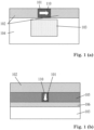
- FIG. 1 shows cross-sectional views illustrating examples of a nonlinear elements, more specifically the terahertz antenna arms forming the plasmonic slot waveguide for the propagation of optical signals.
- the cross-section is taken from the transverse plane of waveguide propagation.
- FIG. 1 (a) illustrates structured nonlinear material 101 with two metal electrodes 102 forming a plasmonic slot, and providing conductive material for the terahertz antenna.
- a (second) photonic waveguide 103 buried in the substrate 104 provides an access waveguide for optical pump signals.
- Light propagating in the higher refractive index material defining the photonic waveguide 103 is evanescently coupled to the plasmonic slot waveguide.
- the optical energy now propagates as surface plasmon polaritons (SPP) at the metal-insulator-metal interface.
- SPP surface plasmon polaritons
- the electric field of the propagating plasmonic mode is symbolized by an arrow 110.
- the plasmonic nature of the slot waveguide provides extreme sub-diffraction confinement of the optical field allowing an electrode spacing on the order of 100nm. This strong confinement of the optical pump signals leads to very strong optical intensities, essential for strong nonlinear effects.
- a terahertz wave incident onto the antenna results in a voltage across the two electrodes 102, and thus the antenna arms.
- This voltage across the nano-scale antenna gap leads to very strong terahertz electric fields in the nonlinear material 101 with same polarization orientation as an optical probe signal propagating along the plasmonic waveguide 110.
- the almost perfect overlap between the optical and the terahertz electric fields, and the strong field enhancement provided by the nano-scale slot result in a very strong and efficient nonlinear interaction between the optical and terahertz signals in the nonlinear material for terahertz wave detection.
- This implementation provides an efficient way to map the information contained in the terahertz on an optical carrier, providing an efficient terahertz wave detection.
- FIG. 1 (b) illustrates a vertical metal-insulator-metal waveguide.
- a bottom conductive electrode 106 such as a metal, a semimetal or transparent conductive oxide (TCO) is deposited on a substrate 103.
- the nonlinear material 101 on top of the first electrode can be structured, e.g. nanorods, or simply a thin fil. In case of a structured nonlinear material 101, an insulating layer 105 can be present present present.
- the top electrode 102 is acting as a top cladding. In such a vertical MIM waveguide, coupled/in light would propagate as SPP confined between the top and bottom electrodes.
- FIG. 2 illustrates a perspective view of an example of a terahertz detection and generation device comprising of a plasmonic waveguide and a terahertz antenna.
- the plasmonic waveguide is a metal-insulator-metal (MIM) slot waveguide formed by the antenna arms 201 and the nonlinear material as the core 202, present on a substrate 203.
- the metal can be either a metal or a semimetal.
- the antenna comprises two antenna arms 201 in form of four-clover-leave shape. Many other possible antenna shapes would work similarly, e.g. Bow-Tie and Yagi-Uda antennas.
- the core material 202 is a e.g. a second order nonlinear ferroelectric material, polymer or crystal.
- the nonlinear material could also rely on a third order nonlinear effect.
- Excited surface plasmon polaritons (SPP) propagating along the MIM slot waveguide are strongly confined inside of the plasmonic waveguide, leading to very high optical intensities in the nonlinear material.
- Two propagating SPP in the plasmonic slot result in generation of sum- and difference-frequency signals.
- Of interest for terahertz generation is mainly the difference-frequency generation (DFG) of two SPP with optical frequency SPP.
- DFG difference-frequency generation
- the resulting terahertz field is efficiently radiated in the far field by the terahertz antenna. This implementation would act as an efficient terahertz wave generation device.
- a terahertz wave incident on the antenna induces an oscillating current in the conductive antenna arms. Electrical charges accumulate at the antenna gap, resulting in a voltage across the slot. The voltage across the nano-scale slot results in a very strong terahertz electric field in the nonlinear material 202.
- the resonant nature of the antenna additionally enhances the terahertz electric field in the nonlinear material.
- the resulting terahertz electric field in the nonlinear material can interact with a propagating SPP of optical frequencies, and translate the information carried by the incident terahertz wave to the optical signal by means of sum-frequency generation.
- FIG. 3 shows cross-sectional illustrations of possible coupling schemes between free-space electromagnetic waves, in particular infrared, visible or ultra-violet light, and the first waveguide, i.e. the plasmonic waveguide.
- FIG. 3 (a) illustrates one embodiment in which the top silicon layer of a silicon-on-insulator (SOI) wafer 301 is selectively etched to pattern (second) photonic waveguides 302.
- This photonic waveguide is used to guide optical signals, e.g. coupled from a laser or fiber by means of grating coupler or edge coupling 303.
- the optical signal from the photonic waveguide couples to the plasmonic evanescently.
- the silicon waveguide 302 is tapered down to enhance the coupling efficiency from the photonic waveguide to the metal-insulator-metal (MIM) interface formed by the terahertz antenna arms 304 and the core 305 comprising the nonlinear material, i.e.
- MIM metal-insulator-metal
- FIG. 3 (b) illustrates an efficient coupling scheme between a free-space optical signal 307, and a plasmonic slot waveguide 305, by means of a diffractive optical element 308.
- the optical element is in close proximity with the plasmonic slot waveguide and structured in form of a focusing grating made of silicon.
- a free-space optical signal is diffracted by the grating and focused towards the plasmonic slot.
- the optical signal is evanescently coupled to the metal-insulator-metal interfaces. This provides an efficient scheme for coupling free-space electromagnetic waves in (307) and out (309) of the plasmonic waveguide.
- FIG. 4 shows an implementation example of a terahertz detector with an integrated Mach-Zehnder interferometer. This enables direct translation of the terahertz information to an amplitude modulation of an optical carrier signal (probe signal).
- the optical signal guided by a silicon waveguide 401 is split in two path, e.g. by a Y-splitter or multi-mode interferometer (MMI). Both silicon waveguide branches couple evanescently in close proximity with a (first) plasmonic waveguide.
- the plasmonic waveguide comprises the nonlinear material 402 and conductive electrodes, formed by portions of the antenna arms 403. The two inner electrodes interface both waveguide cores, thus functioning as claddings.
- the two antenna arms form the outer electrodes.
- An incident terahertz wave produces a voltage across both antenna gaps, which contain the nonlinear material 402.
- the terahertz electric field in the nonlinear material 402 changes the real part of the refractive index, thus inducing a phase shift of the optical signal (probe signal) proportional to the applied voltage.
- an opposite bias voltage between the outer and inner electrodes of the two plasmonic slot, an opposite phase shift can be induced.
- An induced ⁇ -phase shift difference between both plasmonic waveguides would result in destructive interference at the output combiner. This way one can modulate the intensity of the optical probe signal.
- Fig. 5 schematically illustrates a method for manufacturing a terahertz device.
- the first wafer comprises a layer of a nonlinear material (indicated in Fig. 5 as "Epi-ferroelectric), which can be, e.g., an epitaxially grown layer of a ferromagnetic material.
- the layer of nonlinear material is buried.
- possibly existing layers which are not required in the terahertz device are removed.
- the nonlinear material is structured so as to form a waveguide core (of a first - plasmonic - waveguide), and a layer of the second wafer is structure so as to form another waverguide core (of a second waveguide, such as a waveguide for probing and/or pumping).
- a layer of the second wafer is structure so as to form another waverguide core (of a second waveguide, such as a waveguide for probing and/or pumping).
- a second waveguide core of a second waveguide, such as a waveguide for probing and/or pumping.
- Electrodes are produced close to the first core, e.g., by selective metal deposition.
- the first wafer is made of the nonlinear material (possibly with an adhesion layer added).
- the core of the second waveguide from a layer of the second wafer, such as from the layer below the (optional) adhesion layer, such as from the layer indicated "Si" in Fig. 5 .
Landscapes
- Physics & Mathematics (AREA)
- Nonlinear Science (AREA)
- General Physics & Mathematics (AREA)
- Chemical & Material Sciences (AREA)
- Optics & Photonics (AREA)
- Engineering & Computer Science (AREA)
- Ceramic Engineering (AREA)
- Crystallography & Structural Chemistry (AREA)
- Spectroscopy & Molecular Physics (AREA)
- Health & Medical Sciences (AREA)
- Toxicology (AREA)
- Life Sciences & Earth Sciences (AREA)
- Analytical Chemistry (AREA)
- Biochemistry (AREA)
- General Health & Medical Sciences (AREA)
- Immunology (AREA)
- Pathology (AREA)
- Optical Modulation, Optical Deflection, Nonlinear Optics, Optical Demodulation, Optical Logic Elements (AREA)
Claims (10)
- Terahertz-Vorrichtung zum Detektieren oder Emittieren oder sowohl zum Detektieren als auch zum Emittieren von elektromagnetischen Wellen im Terahertz-Bereich, wobei die Vorrichtung auf einem Substrat einen ersten Wellenleiter umfasst, der ein plasmonischer Wellenleiter ist, aufweisend- einen ersten Kern mit einem nichtlinearen Material (101, 202, 305, 402), insbesondere einem ferroelektrischen Material; und- eine Ummantelung, die einen ersten Mantelabschnitt umfasst, der an einer ersten Grenzfläche mit dem ersten Kern, insbesondere mit dem nichtlinearen Material, ein erstes Mantelmaterial umfasst, das ein elektrisch leitendes Material ist;wobei die Vorrichtung eine erste und eine zweite Elektrode (102) umfasst, die in der Nähe des ersten Wellenleiters angeordnet sind,wobei die Vorrichtung eine Antenne mit einem ersten und einem zweiten Arm (201, 304, 403) zum Empfangen oder zum Aussenden oder sowohl zum Empfangen als auch zum Aussenden von elektromagnetischen Wellen im Terahertzbereich umfasst,wobei die Vorrichtung einen zweiten Wellenleiter (103, 302, 401) umfasst, wobei der zweite Wellenleiter ein photonischer Wellenleiter ist, der einen zweiten Kern umfasst, der in der Nähe des ersten Wellenleiters angeordnet ist, um eine Kopplung zwischen dem ersten und dem zweiten Wellenleiter zu ermöglichen,dadurch gekennzeichnet, dass- der zweite Wellenleiter vertikal zwischen dem Substrat (104, 203, 301) und dem ersten Wellenleiter angeordnet ist; und/oder- der zweite Wellenleiter in dem Substrat vergraben ist; und/oder- die Vorrichtung ein integriertes Mach-Zehnder-Interferometer umfasst, indem der zweite Wellenleiter (401) in zwei Zweige aufgeteilt ist, wobei beide Zweige so angeordnet sind, dass sie in unmittelbarer Nähe zu einem ersten Wellenleiter evaneszent koppeln, wobei die Vorrichtung zwei innere Elektroden umfasst, die als Ummantelung fungieren, und zwei äußere Elektroden, die durch die Antennenarme 403 gebildet werden.
- Vorrichtung nach Anspruch 1, wobei die Vorrichtung ein Terahertz-Sender zum Aussenden von elektromagnetischen Wellen im Terahertz-Bereich ist und wobei die erste und die zweite Elektrode (102) zum Aufnehmen eines in dem nichtlinearen Material (101, 202, 305, 402) vorhandenen elektrischen Feldes vorgesehen sind.
- Vorrichtung nach Anspruch 1, wobei die Vorrichtung ein Terahertz-Detektor zum Erfassen von elektromagnetischen Wellen im Terahertz-Bereich ist, und wobei die erste und die zweite Elektrode (102) zum Erzeugen eines elektrischen Feldes in dem nichtlinearen Material (101, 202, 305, 402) vorgesehen sind, wenn zwischen der ersten und der zweiten Elektrode eine Spannung angelegt wird, um eine optische Eigenschaft des nichtlinearen Materials zu modulieren, wie zum Beispiel zum Modulieren mindestens eines Realteils eines Brechungsindexes des nichtlinearen Materials.
- Vorrichtung nach einem der Ansprüche 1 bis 3, wobei die erste Elektrode den ersten Mantelabschnitt bildet, insbesondere wobei das erste Mantelmaterial ein metallisches Material ist.
- Vorrichtung nach einem der Ansprüche 1 bis 4, wobei die Ummantelung einen zweiten, vom ersten Mantelabschnitt getrennten Mantelabschnitt umfasst, der an einer zweiten Grenzfläche mit dem ferroelektrischen Material ein zweites Mantelmaterial umfasst, das ein elektrisch leitendes Material ist.
- Vorrichtung nach Anspruch 5, wobei das nichtlineare Material (101, 202, 305, 402) zwischen dem ersten und dem zweiten Mantelabschnitt angeordnet ist, insbesondere seitlich angeordnet ist, insbesondere wobei die erste Elektrode den ersten Mantelabschnitt und die zweite Elektrode den zweiten Mantelabschnitt bildet.
- Vorrichtung nach einem der Ansprüche 1 bis 6, wobei die ermöglichte Kopplung eine evaneszente Kopplung ist.
- Vorrichtung nach einem der Ansprüche 1 bis 7, umfassend eine optische Struktur, insbesondere eine diffraktive optische Struktur (308), zum Verbessern einer Kopplung zwischen freien elektromagnetischen Wellen, insbesondere freien elektromagnetischen Wellen im infraroten, im sichtbaren oder im ultravioletten Bereich, und dem ersten Wellenleiter, insbesondere wobei die optische Struktur eine fokussierende optische Struktur ist.
- Vorrichtung nach einem der Ansprüche 1-8, wobei das nichtlineare Material ein einkristallines Material, ein polykristallines Material oder ein nanostrukturiertes Material ist.
- Die Vorrichtung nach einem der Ansprüche 1-8, wobei das nichtlineare Material ein amorphes Material ist.
Applications Claiming Priority (2)
| Application Number | Priority Date | Filing Date | Title |
|---|---|---|---|
| CH3742017 | 2017-03-21 | ||
| PCT/EP2018/056925 WO2018172302A1 (en) | 2017-03-21 | 2018-03-20 | DEVICE FOR THz GENERATION AND/OR DETECTION AND METHODS FOR MANUFACTURING THE SAME |
Publications (2)
| Publication Number | Publication Date |
|---|---|
| EP3602188A1 EP3602188A1 (de) | 2020-02-05 |
| EP3602188B1 true EP3602188B1 (de) | 2023-07-12 |
Family
ID=61750120
Family Applications (1)
| Application Number | Title | Priority Date | Filing Date |
|---|---|---|---|
| EP18712572.9A Active EP3602188B1 (de) | 2017-03-21 | 2018-03-20 | Vorrichtung zur thz-erzeugung und/oder -detektion und verfahren zur herstellung davon |
Country Status (5)
| Country | Link |
|---|---|
| US (1) | US11499915B2 (de) |
| EP (1) | EP3602188B1 (de) |
| JP (1) | JP7194444B2 (de) |
| CA (1) | CA3053333A1 (de) |
| WO (1) | WO2018172302A1 (de) |
Families Citing this family (12)
| Publication number | Priority date | Publication date | Assignee | Title |
|---|---|---|---|---|
| US12147098B2 (en) * | 2019-07-24 | 2024-11-19 | Nippon Telegraph And Telephone Corporation | Plasmonic waveguide |
| EP4054074B8 (de) * | 2021-03-03 | 2025-02-12 | Terra Quantum AG | Ferroelektrischer terahertz-resonator |
| CN113093330A (zh) * | 2021-03-24 | 2021-07-09 | 深圳大学 | 非线性狭缝光波导和及其制备方法和应用 |
| CN113670848B (zh) * | 2021-08-23 | 2022-08-02 | 中国人民解放军军事科学院国防科技创新研究院 | 基于像素化结构的高分辨率宽带太赫兹探测器和探测方法 |
| WO2023153138A1 (ja) * | 2022-02-14 | 2023-08-17 | ソニーグループ株式会社 | 波動制御装置、波長変換素子、演算素子、センサ、偏光制御素子及び光アイソレータ |
| DE102022202028A1 (de) | 2022-02-28 | 2023-08-31 | Volkswagen Aktiengesellschaft | Radarsensorvorrichtung für ein Fahrzeug, sowie Radarsystem mit einer Radarsensorvorrichtung und Fahrzeug mit einem Radarsystem |
| CN114779277B (zh) * | 2022-04-29 | 2026-02-13 | 深圳市速腾聚创科技有限公司 | 调频连续波激光雷达 |
| CN116297303B (zh) * | 2023-03-01 | 2025-12-02 | 之江实验室 | 宽带增强指纹谱传感器、太赫兹微结构宽带增强指纹谱检测装置及方法 |
| US12431637B2 (en) | 2023-06-23 | 2025-09-30 | Ecole Polytechnique Federale De Lausanne (Epfl) | On-chip terahertz thin-film devices |
| CN118610281B (zh) * | 2024-04-25 | 2025-04-04 | 广东工业大学 | 一种光电导太赫兹光混频芯片及其制备方法和应用 |
| CN118276228A (zh) * | 2024-06-04 | 2024-07-02 | 深圳北航新兴产业技术研究院 | 太赫兹波合成的集成自旋波导芯片 |
| WO2026017265A1 (en) | 2024-07-19 | 2026-01-22 | Polariton Technologies Ag | Manufacturing method for integrated optics devices with a poled element |
Citations (1)
| Publication number | Priority date | Publication date | Assignee | Title |
|---|---|---|---|---|
| FR2854504A1 (fr) * | 2003-04-30 | 2004-11-05 | Thales Sa | Source d'emission terahertz et systeme optique comprenant une telle source |
Family Cites Families (13)
| Publication number | Priority date | Publication date | Assignee | Title |
|---|---|---|---|---|
| US6967347B2 (en) * | 2001-05-21 | 2005-11-22 | The Regents Of The University Of Colorado | Terahertz interconnect system and applications |
| US7126151B2 (en) * | 2001-05-21 | 2006-10-24 | The Regents Of The University Of Colorado, A Body Corporate | Interconnected high speed electron tunneling devices |
| AU2003233704A1 (en) * | 2002-05-31 | 2003-12-19 | Spectalis Corp. | Electro-optic modulators |
| JP4794878B2 (ja) * | 2004-03-26 | 2011-10-19 | キヤノン株式会社 | 光伝導素子 |
| US7515801B2 (en) * | 2006-12-28 | 2009-04-07 | Wisconsin Alumni Research Foundation | Coherent terahertz radiation source |
| JP5419411B2 (ja) * | 2008-10-08 | 2014-02-19 | キヤノン株式会社 | テラヘルツ波発生素子 |
| JP5709562B2 (ja) | 2010-03-04 | 2015-04-30 | キヤノン株式会社 | テラヘルツ波発生素子、およびテラヘルツ時間領域分光装置 |
| JP2014165412A (ja) * | 2013-02-27 | 2014-09-08 | Seiko Epson Corp | 短光パルス発生装置、テラヘルツ波発生装置、カメラ、イメージング装置、および計測装置 |
| JP2014207654A (ja) * | 2013-03-16 | 2014-10-30 | キヤノン株式会社 | 導波路素子 |
| JP2015118244A (ja) * | 2013-12-18 | 2015-06-25 | セイコーエプソン株式会社 | 短光パルス発生装置、テラヘルツ波発生装置、カメラ、イメージング装置、および計測装置 |
| US9442314B2 (en) | 2014-08-12 | 2016-09-13 | Oracle International Corporation | Ferroelectric-enhanced tuning of ring resonators by using fields parallel to and above a top surface thereof |
| JP6096725B2 (ja) * | 2014-09-09 | 2017-03-15 | アイシン精機株式会社 | 膜厚測定装置及び膜厚測定方法 |
| EP3278177B1 (de) * | 2015-04-01 | 2021-03-31 | ETH Zürich | Elektro-optischer modulator |
-
2018
- 2018-03-20 EP EP18712572.9A patent/EP3602188B1/de active Active
- 2018-03-20 CA CA3053333A patent/CA3053333A1/en active Pending
- 2018-03-20 JP JP2019552053A patent/JP7194444B2/ja active Active
- 2018-03-20 WO PCT/EP2018/056925 patent/WO2018172302A1/en not_active Ceased
- 2018-03-20 US US16/495,178 patent/US11499915B2/en active Active
Patent Citations (1)
| Publication number | Priority date | Publication date | Assignee | Title |
|---|---|---|---|---|
| FR2854504A1 (fr) * | 2003-04-30 | 2004-11-05 | Thales Sa | Source d'emission terahertz et systeme optique comprenant une telle source |
Non-Patent Citations (3)
| Title |
|---|
| BURLA MAURIZIO ET AL: "Microwave plasmonics: A novel platform for RF photonics", 2016 IEEE INTERNATIONAL TOPICAL MEETING ON MICROWAVE PHOTONICS (MWP), IEEE, 31 October 2016 (2016-10-31), pages 259 - 262, XP033035759, DOI: 10.1109/MWP.2016.7791329 * |
| SALAMIN Y ET AL: "Direct RF-to-optical detection by plasmonic modulator integrated into a four-leaf-clover antenna", 2016 CONFERENCE ON LASERS AND ELECTRO-OPTICS (CLEO), OSA, 5 June 2016 (2016-06-05), pages 1 - 2, XP033025570 * |
| SALAMIN YANNICK ET AL: "Direct Conversion of Free Space Millimeter Waves to Optical Domain by Plasmonic Modulator Antenna", NANO LETTERS, vol. 15, no. 12, 19 November 2015 (2015-11-19), US, pages 8342 - 8346, XP055802104, ISSN: 1530-6984, DOI: 10.1021/acs.nanolett.5b04025 * |
Also Published As
| Publication number | Publication date |
|---|---|
| US11499915B2 (en) | 2022-11-15 |
| EP3602188A1 (de) | 2020-02-05 |
| JP7194444B2 (ja) | 2022-12-22 |
| JP2020512585A (ja) | 2020-04-23 |
| US20200408677A1 (en) | 2020-12-31 |
| WO2018172302A1 (en) | 2018-09-27 |
| CA3053333A1 (en) | 2018-09-27 |
Similar Documents
| Publication | Publication Date | Title |
|---|---|---|
| EP3602188B1 (de) | Vorrichtung zur thz-erzeugung und/oder -detektion und verfahren zur herstellung davon | |
| CN107430297B (zh) | 电光调制器 | |
| EP3691033B1 (de) | Optische phasengesteuerte gruppenantenne und lidar damit | |
| US9599770B2 (en) | Graphene photonics for resonator-enhanced electro-optic devices and all-optical interactions | |
| US8311374B2 (en) | Beam generation and steering with integrated optical circuits for light detection and ranging | |
| US9304373B2 (en) | Terahertz wave generation element, terahertz wave detection element, and terahertz time domain spectroscope device | |
| Olivieri et al. | Plasmonic nanostructured metal–oxide–semiconductor reflection modulators | |
| Fedeli et al. | Mid-infrared (Mid-IR) silicon-based photonics | |
| US7783199B2 (en) | Frequency selective MMW source | |
| US20220326438A1 (en) | A plasmonic device enabling simplified fabrication | |
| US20110170820A1 (en) | Eo polymer-based dual slot waveguide modulators | |
| US8909002B2 (en) | Light modulator, optical pickup, and light modulation module | |
| US10261390B2 (en) | Laser beam steering device and system including the same | |
| US20230168561A1 (en) | Electro-optical modulators and applications based on silicon processing compatible nonlinear optical materials | |
| Bavil et al. | Active unidirectional propagation of surface plasmons at subwavelength slits | |
| Feutmba et al. | High frequency characterization of PZT thin-films deposited by chemical solution deposition on SOI for integrated high speed electro-optic modulators | |
| US8780431B1 (en) | Plasmon absorption modulator systems and methods | |
| US11243419B2 (en) | Electro-optic silicon nitride via electric poling | |
| US20080112705A1 (en) | Frequency selective mmw source | |
| Wang et al. | Active beam steering enabled by photonic-crystal surface-emitting laser | |
| US7283704B2 (en) | Optical signal-electric signal converter | |
| Dokhanian et al. | Plasmonic lattice excitation of surface acoustic waves in silicon photonic circuits | |
| Shafir et al. | Surface acoustic wave–photonic devices in silicon nitride integrated circuits | |
| US12547048B1 (en) | Electro-optic THZ emitter and receiver devices and method of fabrication |
Legal Events
| Date | Code | Title | Description |
|---|---|---|---|
| STAA | Information on the status of an ep patent application or granted ep patent |
Free format text: STATUS: UNKNOWN |
|
| STAA | Information on the status of an ep patent application or granted ep patent |
Free format text: STATUS: THE INTERNATIONAL PUBLICATION HAS BEEN MADE |
|
| PUAI | Public reference made under article 153(3) epc to a published international application that has entered the european phase |
Free format text: ORIGINAL CODE: 0009012 |
|
| STAA | Information on the status of an ep patent application or granted ep patent |
Free format text: STATUS: REQUEST FOR EXAMINATION WAS MADE |
|
| 17P | Request for examination filed |
Effective date: 20190913 |
|
| AK | Designated contracting states |
Kind code of ref document: A1 Designated state(s): AL AT BE BG CH CY CZ DE DK EE ES FI FR GB GR HR HU IE IS IT LI LT LU LV MC MK MT NL NO PL PT RO RS SE SI SK SM TR |
|
| AX | Request for extension of the european patent |
Extension state: BA ME |
|
| DAV | Request for validation of the european patent (deleted) | ||
| DAX | Request for extension of the european patent (deleted) | ||
| STAA | Information on the status of an ep patent application or granted ep patent |
Free format text: STATUS: EXAMINATION IS IN PROGRESS |
|
| 17Q | First examination report despatched |
Effective date: 20210528 |
|
| GRAP | Despatch of communication of intention to grant a patent |
Free format text: ORIGINAL CODE: EPIDOSNIGR1 |
|
| STAA | Information on the status of an ep patent application or granted ep patent |
Free format text: STATUS: GRANT OF PATENT IS INTENDED |
|
| INTG | Intention to grant announced |
Effective date: 20230201 |
|
| GRAS | Grant fee paid |
Free format text: ORIGINAL CODE: EPIDOSNIGR3 |
|
| GRAA | (expected) grant |
Free format text: ORIGINAL CODE: 0009210 |
|
| STAA | Information on the status of an ep patent application or granted ep patent |
Free format text: STATUS: THE PATENT HAS BEEN GRANTED |
|
| AK | Designated contracting states |
Kind code of ref document: B1 Designated state(s): AL AT BE BG CH CY CZ DE DK EE ES FI FR GB GR HR HU IE IS IT LI LT LU LV MC MK MT NL NO PL PT RO RS SE SI SK SM TR |
|
| P01 | Opt-out of the competence of the unified patent court (upc) registered |
Effective date: 20230530 |
|
| REG | Reference to a national code |
Ref country code: CH Ref legal event code: EP |
|
| REG | Reference to a national code |
Ref country code: DE Ref legal event code: R096 Ref document number: 602018053165 Country of ref document: DE |
|
| REG | Reference to a national code |
Ref country code: IE Ref legal event code: FG4D |
|
| REG | Reference to a national code |
Ref country code: LT Ref legal event code: MG9D |
|
| REG | Reference to a national code |
Ref country code: NL Ref legal event code: MP Effective date: 20230712 |
|
| REG | Reference to a national code |
Ref country code: AT Ref legal event code: MK05 Ref document number: 1587771 Country of ref document: AT Kind code of ref document: T Effective date: 20230712 |
|
| PG25 | Lapsed in a contracting state [announced via postgrant information from national office to epo] |
Ref country code: NL Free format text: LAPSE BECAUSE OF FAILURE TO SUBMIT A TRANSLATION OF THE DESCRIPTION OR TO PAY THE FEE WITHIN THE PRESCRIBED TIME-LIMIT Effective date: 20230712 |
|
| PG25 | Lapsed in a contracting state [announced via postgrant information from national office to epo] |
Ref country code: GR Free format text: LAPSE BECAUSE OF FAILURE TO SUBMIT A TRANSLATION OF THE DESCRIPTION OR TO PAY THE FEE WITHIN THE PRESCRIBED TIME-LIMIT Effective date: 20231013 |
|
| PG25 | Lapsed in a contracting state [announced via postgrant information from national office to epo] |
Ref country code: ES Free format text: LAPSE BECAUSE OF FAILURE TO SUBMIT A TRANSLATION OF THE DESCRIPTION OR TO PAY THE FEE WITHIN THE PRESCRIBED TIME-LIMIT Effective date: 20230712 |
|
| PG25 | Lapsed in a contracting state [announced via postgrant information from national office to epo] |
Ref country code: IS Free format text: LAPSE BECAUSE OF FAILURE TO SUBMIT A TRANSLATION OF THE DESCRIPTION OR TO PAY THE FEE WITHIN THE PRESCRIBED TIME-LIMIT Effective date: 20231112 |
|
| PG25 | Lapsed in a contracting state [announced via postgrant information from national office to epo] |
Ref country code: SE Free format text: LAPSE BECAUSE OF FAILURE TO SUBMIT A TRANSLATION OF THE DESCRIPTION OR TO PAY THE FEE WITHIN THE PRESCRIBED TIME-LIMIT Effective date: 20230712 Ref country code: RS Free format text: LAPSE BECAUSE OF FAILURE TO SUBMIT A TRANSLATION OF THE DESCRIPTION OR TO PAY THE FEE WITHIN THE PRESCRIBED TIME-LIMIT Effective date: 20230712 Ref country code: PT Free format text: LAPSE BECAUSE OF FAILURE TO SUBMIT A TRANSLATION OF THE DESCRIPTION OR TO PAY THE FEE WITHIN THE PRESCRIBED TIME-LIMIT Effective date: 20231113 Ref country code: NO Free format text: LAPSE BECAUSE OF FAILURE TO SUBMIT A TRANSLATION OF THE DESCRIPTION OR TO PAY THE FEE WITHIN THE PRESCRIBED TIME-LIMIT Effective date: 20231012 Ref country code: LV Free format text: LAPSE BECAUSE OF FAILURE TO SUBMIT A TRANSLATION OF THE DESCRIPTION OR TO PAY THE FEE WITHIN THE PRESCRIBED TIME-LIMIT Effective date: 20230712 Ref country code: LT Free format text: LAPSE BECAUSE OF FAILURE TO SUBMIT A TRANSLATION OF THE DESCRIPTION OR TO PAY THE FEE WITHIN THE PRESCRIBED TIME-LIMIT Effective date: 20230712 Ref country code: IS Free format text: LAPSE BECAUSE OF FAILURE TO SUBMIT A TRANSLATION OF THE DESCRIPTION OR TO PAY THE FEE WITHIN THE PRESCRIBED TIME-LIMIT Effective date: 20231112 Ref country code: HR Free format text: LAPSE BECAUSE OF FAILURE TO SUBMIT A TRANSLATION OF THE DESCRIPTION OR TO PAY THE FEE WITHIN THE PRESCRIBED TIME-LIMIT Effective date: 20230712 Ref country code: GR Free format text: LAPSE BECAUSE OF FAILURE TO SUBMIT A TRANSLATION OF THE DESCRIPTION OR TO PAY THE FEE WITHIN THE PRESCRIBED TIME-LIMIT Effective date: 20231013 Ref country code: FI Free format text: LAPSE BECAUSE OF FAILURE TO SUBMIT A TRANSLATION OF THE DESCRIPTION OR TO PAY THE FEE WITHIN THE PRESCRIBED TIME-LIMIT Effective date: 20230712 Ref country code: ES Free format text: LAPSE BECAUSE OF FAILURE TO SUBMIT A TRANSLATION OF THE DESCRIPTION OR TO PAY THE FEE WITHIN THE PRESCRIBED TIME-LIMIT Effective date: 20230712 Ref country code: AT Free format text: LAPSE BECAUSE OF FAILURE TO SUBMIT A TRANSLATION OF THE DESCRIPTION OR TO PAY THE FEE WITHIN THE PRESCRIBED TIME-LIMIT Effective date: 20230712 |
|
| PG25 | Lapsed in a contracting state [announced via postgrant information from national office to epo] |
Ref country code: PL Free format text: LAPSE BECAUSE OF FAILURE TO SUBMIT A TRANSLATION OF THE DESCRIPTION OR TO PAY THE FEE WITHIN THE PRESCRIBED TIME-LIMIT Effective date: 20230712 |
|
| REG | Reference to a national code |
Ref country code: DE Ref legal event code: R097 Ref document number: 602018053165 Country of ref document: DE |
|
| PG25 | Lapsed in a contracting state [announced via postgrant information from national office to epo] |
Ref country code: SM Free format text: LAPSE BECAUSE OF FAILURE TO SUBMIT A TRANSLATION OF THE DESCRIPTION OR TO PAY THE FEE WITHIN THE PRESCRIBED TIME-LIMIT Effective date: 20230712 Ref country code: RO Free format text: LAPSE BECAUSE OF FAILURE TO SUBMIT A TRANSLATION OF THE DESCRIPTION OR TO PAY THE FEE WITHIN THE PRESCRIBED TIME-LIMIT Effective date: 20230712 Ref country code: EE Free format text: LAPSE BECAUSE OF FAILURE TO SUBMIT A TRANSLATION OF THE DESCRIPTION OR TO PAY THE FEE WITHIN THE PRESCRIBED TIME-LIMIT Effective date: 20230712 Ref country code: DK Free format text: LAPSE BECAUSE OF FAILURE TO SUBMIT A TRANSLATION OF THE DESCRIPTION OR TO PAY THE FEE WITHIN THE PRESCRIBED TIME-LIMIT Effective date: 20230712 Ref country code: CZ Free format text: LAPSE BECAUSE OF FAILURE TO SUBMIT A TRANSLATION OF THE DESCRIPTION OR TO PAY THE FEE WITHIN THE PRESCRIBED TIME-LIMIT Effective date: 20230712 Ref country code: SK Free format text: LAPSE BECAUSE OF FAILURE TO SUBMIT A TRANSLATION OF THE DESCRIPTION OR TO PAY THE FEE WITHIN THE PRESCRIBED TIME-LIMIT Effective date: 20230712 |
|
| PLBE | No opposition filed within time limit |
Free format text: ORIGINAL CODE: 0009261 |
|
| STAA | Information on the status of an ep patent application or granted ep patent |
Free format text: STATUS: NO OPPOSITION FILED WITHIN TIME LIMIT |
|
| PG25 | Lapsed in a contracting state [announced via postgrant information from national office to epo] |
Ref country code: IT Free format text: LAPSE BECAUSE OF FAILURE TO SUBMIT A TRANSLATION OF THE DESCRIPTION OR TO PAY THE FEE WITHIN THE PRESCRIBED TIME-LIMIT Effective date: 20230712 |
|
| 26N | No opposition filed |
Effective date: 20240415 |
|
| PG25 | Lapsed in a contracting state [announced via postgrant information from national office to epo] |
Ref country code: SI Free format text: LAPSE BECAUSE OF FAILURE TO SUBMIT A TRANSLATION OF THE DESCRIPTION OR TO PAY THE FEE WITHIN THE PRESCRIBED TIME-LIMIT Effective date: 20230712 |
|
| PG25 | Lapsed in a contracting state [announced via postgrant information from national office to epo] |
Ref country code: BG Free format text: LAPSE BECAUSE OF FAILURE TO SUBMIT A TRANSLATION OF THE DESCRIPTION OR TO PAY THE FEE WITHIN THE PRESCRIBED TIME-LIMIT Effective date: 20230712 |
|
| PG25 | Lapsed in a contracting state [announced via postgrant information from national office to epo] |
Ref country code: LU Free format text: LAPSE BECAUSE OF NON-PAYMENT OF DUE FEES Effective date: 20240320 |
|
| PG25 | Lapsed in a contracting state [announced via postgrant information from national office to epo] |
Ref country code: MC Free format text: LAPSE BECAUSE OF FAILURE TO SUBMIT A TRANSLATION OF THE DESCRIPTION OR TO PAY THE FEE WITHIN THE PRESCRIBED TIME-LIMIT Effective date: 20230712 |
|
| PG25 | Lapsed in a contracting state [announced via postgrant information from national office to epo] |
Ref country code: MC Free format text: LAPSE BECAUSE OF FAILURE TO SUBMIT A TRANSLATION OF THE DESCRIPTION OR TO PAY THE FEE WITHIN THE PRESCRIBED TIME-LIMIT Effective date: 20230712 Ref country code: LU Free format text: LAPSE BECAUSE OF NON-PAYMENT OF DUE FEES Effective date: 20240320 Ref country code: BG Free format text: LAPSE BECAUSE OF FAILURE TO SUBMIT A TRANSLATION OF THE DESCRIPTION OR TO PAY THE FEE WITHIN THE PRESCRIBED TIME-LIMIT Effective date: 20230712 |
|
| REG | Reference to a national code |
Ref country code: BE Ref legal event code: MM Effective date: 20240331 |
|
| PG25 | Lapsed in a contracting state [announced via postgrant information from national office to epo] |
Ref country code: BE Free format text: LAPSE BECAUSE OF NON-PAYMENT OF DUE FEES Effective date: 20240331 |
|
| PG25 | Lapsed in a contracting state [announced via postgrant information from national office to epo] |
Ref country code: IE Free format text: LAPSE BECAUSE OF NON-PAYMENT OF DUE FEES Effective date: 20240320 |
|
| PG25 | Lapsed in a contracting state [announced via postgrant information from national office to epo] |
Ref country code: IE Free format text: LAPSE BECAUSE OF NON-PAYMENT OF DUE FEES Effective date: 20240320 Ref country code: BE Free format text: LAPSE BECAUSE OF NON-PAYMENT OF DUE FEES Effective date: 20240331 |
|
| PGFP | Annual fee paid to national office [announced via postgrant information from national office to epo] |
Ref country code: DE Payment date: 20250319 Year of fee payment: 8 |
|
| PGFP | Annual fee paid to national office [announced via postgrant information from national office to epo] |
Ref country code: FR Payment date: 20250326 Year of fee payment: 8 |
|
| PGFP | Annual fee paid to national office [announced via postgrant information from national office to epo] |
Ref country code: GB Payment date: 20250324 Year of fee payment: 8 |
|
| PGFP | Annual fee paid to national office [announced via postgrant information from national office to epo] |
Ref country code: CH Payment date: 20250401 Year of fee payment: 8 |
|
| PG25 | Lapsed in a contracting state [announced via postgrant information from national office to epo] |
Ref country code: CY Free format text: LAPSE BECAUSE OF FAILURE TO SUBMIT A TRANSLATION OF THE DESCRIPTION OR TO PAY THE FEE WITHIN THE PRESCRIBED TIME-LIMIT; INVALID AB INITIO Effective date: 20180320 |
|
| PG25 | Lapsed in a contracting state [announced via postgrant information from national office to epo] |
Ref country code: HU Free format text: LAPSE BECAUSE OF FAILURE TO SUBMIT A TRANSLATION OF THE DESCRIPTION OR TO PAY THE FEE WITHIN THE PRESCRIBED TIME-LIMIT; INVALID AB INITIO Effective date: 20180320 |
|
| PG25 | Lapsed in a contracting state [announced via postgrant information from national office to epo] |
Ref country code: TR Free format text: LAPSE BECAUSE OF FAILURE TO SUBMIT A TRANSLATION OF THE DESCRIPTION OR TO PAY THE FEE WITHIN THE PRESCRIBED TIME-LIMIT Effective date: 20230712 |