EP3602188B1 - Device for thz generation and/or detection and methods for manufacturing the same - Google Patents
Device for thz generation and/or detection and methods for manufacturing the same Download PDFInfo
- Publication number
- EP3602188B1 EP3602188B1 EP18712572.9A EP18712572A EP3602188B1 EP 3602188 B1 EP3602188 B1 EP 3602188B1 EP 18712572 A EP18712572 A EP 18712572A EP 3602188 B1 EP3602188 B1 EP 3602188B1
- Authority
- EP
- European Patent Office
- Prior art keywords
- waveguide
- terahertz
- nonlinear
- cladding
- optical
- Prior art date
- Legal status (The legal status is an assumption and is not a legal conclusion. Google has not performed a legal analysis and makes no representation as to the accuracy of the status listed.)
- Active
Links
- 238000000034 method Methods 0.000 title description 21
- 238000001514 detection method Methods 0.000 title description 19
- 238000004519 manufacturing process Methods 0.000 title description 9
- 239000000463 material Substances 0.000 claims description 117
- 230000003287 optical effect Effects 0.000 claims description 70
- 238000005253 cladding Methods 0.000 claims description 27
- 239000000758 substrate Substances 0.000 claims description 27
- 230000008878 coupling Effects 0.000 claims description 17
- 238000010168 coupling process Methods 0.000 claims description 17
- 238000005859 coupling reaction Methods 0.000 claims description 17
- 230000005684 electric field Effects 0.000 claims description 16
- 239000004020 conductor Substances 0.000 claims description 8
- 239000002178 crystalline material Substances 0.000 claims description 3
- 230000002708 enhancing effect Effects 0.000 claims description 3
- 239000007769 metal material Substances 0.000 claims description 2
- 239000002086 nanomaterial Substances 0.000 claims description 2
- 235000012431 wafers Nutrition 0.000 description 41
- 239000011162 core material Substances 0.000 description 25
- 239000013078 crystal Substances 0.000 description 14
- 229910052751 metal Inorganic materials 0.000 description 14
- 239000002184 metal Substances 0.000 description 14
- 230000001902 propagating effect Effects 0.000 description 9
- 239000000523 sample Substances 0.000 description 9
- 230000008901 benefit Effects 0.000 description 8
- 239000012071 phase Substances 0.000 description 7
- 230000005855 radiation Effects 0.000 description 7
- 238000005516 engineering process Methods 0.000 description 6
- XUIMIQQOPSSXEZ-UHFFFAOYSA-N Silicon Chemical compound [Si] XUIMIQQOPSSXEZ-UHFFFAOYSA-N 0.000 description 5
- 230000010287 polarization Effects 0.000 description 5
- 229910052710 silicon Inorganic materials 0.000 description 5
- 239000010703 silicon Substances 0.000 description 5
- 229910003781 PbTiO3 Inorganic materials 0.000 description 4
- 239000012212 insulator Substances 0.000 description 4
- 230000003993 interaction Effects 0.000 description 4
- 239000004065 semiconductor Substances 0.000 description 4
- 229910003327 LiNbO3 Inorganic materials 0.000 description 3
- 229910019653 Mg1/3Nb2/3 Inorganic materials 0.000 description 3
- 238000013459 approach Methods 0.000 description 3
- 239000000969 carrier Substances 0.000 description 3
- 238000006243 chemical reaction Methods 0.000 description 3
- 229910021419 crystalline silicon Inorganic materials 0.000 description 3
- 230000009022 nonlinear effect Effects 0.000 description 3
- 230000010363 phase shift Effects 0.000 description 3
- 229910001218 Gallium arsenide Inorganic materials 0.000 description 2
- 229910020289 Pb(ZrxTi1-x)O3 Inorganic materials 0.000 description 2
- 229910020273 Pb(ZrxTi1−x)O3 Inorganic materials 0.000 description 2
- 229910002113 barium titanate Inorganic materials 0.000 description 2
- 239000002800 charge carrier Substances 0.000 description 2
- 230000001427 coherent effect Effects 0.000 description 2
- 229910052802 copper Inorganic materials 0.000 description 2
- 238000000151 deposition Methods 0.000 description 2
- 239000012777 electrically insulating material Substances 0.000 description 2
- 230000001747 exhibiting effect Effects 0.000 description 2
- 239000000835 fiber Substances 0.000 description 2
- 238000003384 imaging method Methods 0.000 description 2
- 150000002739 metals Chemical class 0.000 description 2
- FGIUAXJPYTZDNR-UHFFFAOYSA-N potassium nitrate Chemical compound [K+].[O-][N+]([O-])=O FGIUAXJPYTZDNR-UHFFFAOYSA-N 0.000 description 2
- 238000003860 storage Methods 0.000 description 2
- 229910052721 tungsten Inorganic materials 0.000 description 2
- 229910017251 AsO4 Inorganic materials 0.000 description 1
- 229910015846 BaxSr1-xTiO3 Inorganic materials 0.000 description 1
- OKTJSMMVPCPJKN-UHFFFAOYSA-N Carbon Chemical compound [C] OKTJSMMVPCPJKN-UHFFFAOYSA-N 0.000 description 1
- 239000007836 KH2PO4 Substances 0.000 description 1
- 229910002340 LaNiO3 Inorganic materials 0.000 description 1
- -1 LaSrCoOs Inorganic materials 0.000 description 1
- 229910019695 Nb2O6 Inorganic materials 0.000 description 1
- 229910002353 SrRuO3 Inorganic materials 0.000 description 1
- 229910007709 ZnTe Inorganic materials 0.000 description 1
- 230000001133 acceleration Effects 0.000 description 1
- 238000004026 adhesive bonding Methods 0.000 description 1
- 229910052782 aluminium Inorganic materials 0.000 description 1
- LFVGISIMTYGQHF-UHFFFAOYSA-N ammonium dihydrogen phosphate Chemical compound [NH4+].OP(O)([O-])=O LFVGISIMTYGQHF-UHFFFAOYSA-N 0.000 description 1
- 230000008859 change Effects 0.000 description 1
- 238000004891 communication Methods 0.000 description 1
- 230000001419 dependent effect Effects 0.000 description 1
- 230000001066 destructive effect Effects 0.000 description 1
- 230000009977 dual effect Effects 0.000 description 1
- 230000000694 effects Effects 0.000 description 1
- 230000005670 electromagnetic radiation Effects 0.000 description 1
- 230000005621 ferroelectricity Effects 0.000 description 1
- 239000003302 ferromagnetic material Substances 0.000 description 1
- 230000006870 function Effects 0.000 description 1
- 229910052737 gold Inorganic materials 0.000 description 1
- 229910021389 graphene Inorganic materials 0.000 description 1
- 238000001727 in vivo Methods 0.000 description 1
- AMGQUBHHOARCQH-UHFFFAOYSA-N indium;oxotin Chemical compound [In].[Sn]=O AMGQUBHHOARCQH-UHFFFAOYSA-N 0.000 description 1
- 230000001939 inductive effect Effects 0.000 description 1
- 230000010354 integration Effects 0.000 description 1
- 238000000608 laser ablation Methods 0.000 description 1
- 238000013507 mapping Methods 0.000 description 1
- 238000001465 metallisation Methods 0.000 description 1
- 238000001451 molecular beam epitaxy Methods 0.000 description 1
- 229910000402 monopotassium phosphate Inorganic materials 0.000 description 1
- 239000002073 nanorod Substances 0.000 description 1
- 239000013307 optical fiber Substances 0.000 description 1
- 230000005693 optoelectronics Effects 0.000 description 1
- 239000011368 organic material Substances 0.000 description 1
- 239000012074 organic phase Substances 0.000 description 1
- 230000010355 oscillation Effects 0.000 description 1
- 229910052697 platinum Inorganic materials 0.000 description 1
- 229920000642 polymer Polymers 0.000 description 1
- GNSKLFRGEWLPPA-UHFFFAOYSA-M potassium dihydrogen phosphate Chemical compound [K+].OP(O)([O-])=O GNSKLFRGEWLPPA-UHFFFAOYSA-M 0.000 description 1
- GVPLVOGUVQAPNJ-UHFFFAOYSA-M potassium;hydron;trioxido(oxo)-$l^{5}-arsane Chemical compound [K+].O[As](O)([O-])=O GVPLVOGUVQAPNJ-UHFFFAOYSA-M 0.000 description 1
- 238000005086 pumping Methods 0.000 description 1
- 230000004044 response Effects 0.000 description 1
- 230000035945 sensitivity Effects 0.000 description 1
- 229910052709 silver Inorganic materials 0.000 description 1
- 238000004611 spectroscopical analysis Methods 0.000 description 1
- 238000001228 spectrum Methods 0.000 description 1
- 238000010183 spectrum analysis Methods 0.000 description 1
- 238000004544 sputter deposition Methods 0.000 description 1
- 238000012731 temporal analysis Methods 0.000 description 1
- 230000002123 temporal effect Effects 0.000 description 1
- 229910052719 titanium Inorganic materials 0.000 description 1
- 238000013519 translation Methods 0.000 description 1
- 238000001771 vacuum deposition Methods 0.000 description 1
Images


Classifications
-
- G—PHYSICS
- G01—MEASURING; TESTING
- G01N—INVESTIGATING OR ANALYSING MATERIALS BY DETERMINING THEIR CHEMICAL OR PHYSICAL PROPERTIES
- G01N21/00—Investigating or analysing materials by the use of optical means, i.e. using sub-millimetre waves, infrared, visible or ultraviolet light
- G01N21/17—Systems in which incident light is modified in accordance with the properties of the material investigated
- G01N21/25—Colour; Spectral properties, i.e. comparison of effect of material on the light at two or more different wavelengths or wavelength bands
- G01N21/31—Investigating relative effect of material at wavelengths characteristic of specific elements or molecules, e.g. atomic absorption spectrometry
- G01N21/35—Investigating relative effect of material at wavelengths characteristic of specific elements or molecules, e.g. atomic absorption spectrometry using infrared light
- G01N21/3581—Investigating relative effect of material at wavelengths characteristic of specific elements or molecules, e.g. atomic absorption spectrometry using infrared light using far infrared light; using Terahertz radiation
- G01N21/3586—Investigating relative effect of material at wavelengths characteristic of specific elements or molecules, e.g. atomic absorption spectrometry using infrared light using far infrared light; using Terahertz radiation by Terahertz time domain spectroscopy [THz-TDS]
-
- G—PHYSICS
- G02—OPTICS
- G02F—OPTICAL DEVICES OR ARRANGEMENTS FOR THE CONTROL OF LIGHT BY MODIFICATION OF THE OPTICAL PROPERTIES OF THE MEDIA OF THE ELEMENTS INVOLVED THEREIN; NON-LINEAR OPTICS; FREQUENCY-CHANGING OF LIGHT; OPTICAL LOGIC ELEMENTS; OPTICAL ANALOGUE/DIGITAL CONVERTERS
- G02F1/00—Devices or arrangements for the control of the intensity, colour, phase, polarisation or direction of light arriving from an independent light source, e.g. switching, gating or modulating; Non-linear optics
- G02F1/01—Devices or arrangements for the control of the intensity, colour, phase, polarisation or direction of light arriving from an independent light source, e.g. switching, gating or modulating; Non-linear optics for the control of the intensity, phase, polarisation or colour
- G02F1/03—Devices or arrangements for the control of the intensity, colour, phase, polarisation or direction of light arriving from an independent light source, e.g. switching, gating or modulating; Non-linear optics for the control of the intensity, phase, polarisation or colour based on ceramics or electro-optical crystals, e.g. exhibiting Pockels effect or Kerr effect
- G02F1/05—Devices or arrangements for the control of the intensity, colour, phase, polarisation or direction of light arriving from an independent light source, e.g. switching, gating or modulating; Non-linear optics for the control of the intensity, phase, polarisation or colour based on ceramics or electro-optical crystals, e.g. exhibiting Pockels effect or Kerr effect with ferro-electric properties
-
- G—PHYSICS
- G02—OPTICS
- G02F—OPTICAL DEVICES OR ARRANGEMENTS FOR THE CONTROL OF LIGHT BY MODIFICATION OF THE OPTICAL PROPERTIES OF THE MEDIA OF THE ELEMENTS INVOLVED THEREIN; NON-LINEAR OPTICS; FREQUENCY-CHANGING OF LIGHT; OPTICAL LOGIC ELEMENTS; OPTICAL ANALOGUE/DIGITAL CONVERTERS
- G02F1/00—Devices or arrangements for the control of the intensity, colour, phase, polarisation or direction of light arriving from an independent light source, e.g. switching, gating or modulating; Non-linear optics
- G02F1/01—Devices or arrangements for the control of the intensity, colour, phase, polarisation or direction of light arriving from an independent light source, e.g. switching, gating or modulating; Non-linear optics for the control of the intensity, phase, polarisation or colour
- G02F1/03—Devices or arrangements for the control of the intensity, colour, phase, polarisation or direction of light arriving from an independent light source, e.g. switching, gating or modulating; Non-linear optics for the control of the intensity, phase, polarisation or colour based on ceramics or electro-optical crystals, e.g. exhibiting Pockels effect or Kerr effect
- G02F1/035—Devices or arrangements for the control of the intensity, colour, phase, polarisation or direction of light arriving from an independent light source, e.g. switching, gating or modulating; Non-linear optics for the control of the intensity, phase, polarisation or colour based on ceramics or electro-optical crystals, e.g. exhibiting Pockels effect or Kerr effect in an optical waveguide structure
-
- G—PHYSICS
- G02—OPTICS
- G02F—OPTICAL DEVICES OR ARRANGEMENTS FOR THE CONTROL OF LIGHT BY MODIFICATION OF THE OPTICAL PROPERTIES OF THE MEDIA OF THE ELEMENTS INVOLVED THEREIN; NON-LINEAR OPTICS; FREQUENCY-CHANGING OF LIGHT; OPTICAL LOGIC ELEMENTS; OPTICAL ANALOGUE/DIGITAL CONVERTERS
- G02F1/00—Devices or arrangements for the control of the intensity, colour, phase, polarisation or direction of light arriving from an independent light source, e.g. switching, gating or modulating; Non-linear optics
- G02F1/01—Devices or arrangements for the control of the intensity, colour, phase, polarisation or direction of light arriving from an independent light source, e.g. switching, gating or modulating; Non-linear optics for the control of the intensity, phase, polarisation or colour
- G02F1/03—Devices or arrangements for the control of the intensity, colour, phase, polarisation or direction of light arriving from an independent light source, e.g. switching, gating or modulating; Non-linear optics for the control of the intensity, phase, polarisation or colour based on ceramics or electro-optical crystals, e.g. exhibiting Pockels effect or Kerr effect
- G02F1/05—Devices or arrangements for the control of the intensity, colour, phase, polarisation or direction of light arriving from an independent light source, e.g. switching, gating or modulating; Non-linear optics for the control of the intensity, phase, polarisation or colour based on ceramics or electro-optical crystals, e.g. exhibiting Pockels effect or Kerr effect with ferro-electric properties
- G02F1/0508—Devices or arrangements for the control of the intensity, colour, phase, polarisation or direction of light arriving from an independent light source, e.g. switching, gating or modulating; Non-linear optics for the control of the intensity, phase, polarisation or colour based on ceramics or electro-optical crystals, e.g. exhibiting Pockels effect or Kerr effect with ferro-electric properties specially adapted for gating or modulating in optical waveguides
-
- G—PHYSICS
- G02—OPTICS
- G02F—OPTICAL DEVICES OR ARRANGEMENTS FOR THE CONTROL OF LIGHT BY MODIFICATION OF THE OPTICAL PROPERTIES OF THE MEDIA OF THE ELEMENTS INVOLVED THEREIN; NON-LINEAR OPTICS; FREQUENCY-CHANGING OF LIGHT; OPTICAL LOGIC ELEMENTS; OPTICAL ANALOGUE/DIGITAL CONVERTERS
- G02F1/00—Devices or arrangements for the control of the intensity, colour, phase, polarisation or direction of light arriving from an independent light source, e.g. switching, gating or modulating; Non-linear optics
- G02F1/01—Devices or arrangements for the control of the intensity, colour, phase, polarisation or direction of light arriving from an independent light source, e.g. switching, gating or modulating; Non-linear optics for the control of the intensity, phase, polarisation or colour
- G02F1/21—Devices or arrangements for the control of the intensity, colour, phase, polarisation or direction of light arriving from an independent light source, e.g. switching, gating or modulating; Non-linear optics for the control of the intensity, phase, polarisation or colour by interference
- G02F1/225—Devices or arrangements for the control of the intensity, colour, phase, polarisation or direction of light arriving from an independent light source, e.g. switching, gating or modulating; Non-linear optics for the control of the intensity, phase, polarisation or colour by interference in an optical waveguide structure
-
- G—PHYSICS
- G02—OPTICS
- G02B—OPTICAL ELEMENTS, SYSTEMS OR APPARATUS
- G02B6/00—Light guides; Structural details of arrangements comprising light guides and other optical elements, e.g. couplings
- G02B6/10—Light guides; Structural details of arrangements comprising light guides and other optical elements, e.g. couplings of the optical waveguide type
- G02B6/12—Light guides; Structural details of arrangements comprising light guides and other optical elements, e.g. couplings of the optical waveguide type of the integrated circuit kind
- G02B6/122—Basic optical elements, e.g. light-guiding paths
- G02B6/1226—Basic optical elements, e.g. light-guiding paths involving surface plasmon interaction
-
- G—PHYSICS
- G02—OPTICS
- G02B—OPTICAL ELEMENTS, SYSTEMS OR APPARATUS
- G02B6/00—Light guides; Structural details of arrangements comprising light guides and other optical elements, e.g. couplings
- G02B6/24—Coupling light guides
- G02B6/42—Coupling light guides with opto-electronic elements
- G02B6/43—Arrangements comprising a plurality of opto-electronic elements and associated optical interconnections
Definitions
- the invention relates to nonlinear elements in which terahertz (THz) frequency electromagnetic waves interact with nonlinear material systems, and to terahertz waves' detection and generation comprising the same. It relates to nonlinear elements, and devices enabling the mapping of a terahertz wave onto an optical frequency carrier, and an optical signal to produce a terahertz signal.
- the invention relates further to methods and apparatuses.
- the devices may find applications, e.g. in terahertz generation and terahertz sensing, terahertz imaging, terahertz communication and terahertz storage.
- Terahertz waves a part of the electromagnetic spectrum unexplored until a decade ago has attracted a lot of attention in recent years.
- Terahertz waves provide several advantages due to their short wavelength providing a strong advantage compared to microwave imaging, transparent property to a lot of materials, and strong sensitivity to a phase change of the material system.
- material systems can respond strongly to terahertz radiation due to molecular vibrational modes, or optical phonon vibrations in crystals. Therefore, strong interest in the science community to find low-cost, power efficient and compact terahertz devices for generation and detection of terahertz waves has driven the terahertz technology.
- Nonlinear terahertz generation and detection is achieved by using the second order nonlinearity of a nonlinear crystal, i.e. ZnTe, GaAs etc.
- a short optical pulse referred to as the pump signal and inherently broadband, propagating through such a nonlinear crystal produces terahertz radiation through self-mixing of all its frequency components.
- the pump signal is split and used as a probe signal to co-propagate through a similar nonlinear crystal along with the terahertz wave to be detected.
- the produced electric field in the crystal by the terahertz wave induces birefringence in the crystal changing the refractive index for one polarization of the crystal. This induces a polarization rotation to the optical pump signal.
- By reading out the polarization rotation of the optical probe signal by means of optoelectronic conversion one can deduce the amplitude of the terahertz field present in the crystal.
- Another technique to generate and detect terahertz signals is based on photoconductive antennas.
- An incident optical pump signal on a high mobility substrate, i.e. GaAs produces charge carriers. In the presence of a strong electric field, these carriers separate rapidly, and their acceleration produces terahertz waves.
- the use of metallic antenna arms to collect the generated carriers and to increase the radiation efficiency of the produced terahertz signal has shown efficient terahertz generation.
- the optical pump is split and used to probe the terahertz signal in a high mobility semiconductor.
- the generated charge carrier by the optical pump drift apart generating a current which can be read and related to the terahertz field amplitude.
- One major drawback of those terahertz systems is the necessity to have both signals, i.e. optical pump and terahertz wave, coherent for time and frequency spectroscopy.
- US 2008/0159342 A1 pertains to terahertz radiation sources having a dual waveguide structure that incorporates both an optical waveguide and a terahertz waveguide. More precisely, the THz radiation source includes an optical waveguide contained within a larger THz waveguide layered structure and it provides a coherent guided wave of THz radiation.
- WO 2016/154764 A2 discloses devices for enabling optical phase, amplitude and intensity modulation.
- the devices are configured to modulate light in the infrared and/or in the visible and/or in the ultraviolet range and for applications such as optical data- and telecommunication, optical storage and optical sensing.
- the devices are able to modulate an optical phase by comprising a first waveguide and first and second electrodes.
- the first waveguide comprises a core of ferroelectric material.
- the first and second electrodes are arranged in a manner to produce an electric field in the ferroelectric material when a voltage is applied between the first and second electrodes.
- the electric field modulates at least the real part of the refractive index of the ferroelectric material and hence modulates the phases of the plasmon polariton modes present at the interface between the core (ferroelectric material) and its cladding.
- M. Brula et al. "Microwave Plasmonics: A Novel Platform for RF Photonics," IEEE International Topical Meeting on Microwave Photonics 2016, pp. 259-262 discusses the potential of the plasmonic platform, this means of surface plasmon polaritons, for microwave photonics applications, in particular for plasmonic organic hybrid modulators.
- D1 discloses plasmonic-photonic Mach-Zehnder Modulators (MZMs), all-plasmonic MZMs and IQ modulators, Plasmonic Phase Modulators (PPMs) co-integrated with antennas, and plasmonic beamforming networks.
- MZMs Mach-Zehnder Modulators
- PPMs Plasmonic Phase Modulators
- the devices comprise a plasmonic organic phase modulator that comprises a single metal-insulator-metal (MIM) slot waveguide, wherein the slot is filled with a nonlinear organic material, and that is co-integrated with an antenna, in particular a four-clover-leaf antenna or a bowtie antenna.
- the devices comprise further a straight, non-splitting photonic waveguide that is arranged on the same plane as the MIM slot waveguide.
- the THz emission source comprises a source device, a guide and a miniature emission head.
- the source device emits two waves that differ in frequency in the order of THz.
- the guide is realized as an optical fiber that is configured to convey the waves to the detection surface of a photodetector arranged in the miniature emission head.
- the photodetector used comprises a nonlinear material and is configured to generate the difference frequency of the two waves.
- the miniature emission head comprises further an antenna configured to emit the generated difference frequency.
- Possible objects of the invention are one or more of
- the device in which terahertz waves interact with light comprises a first antenna which is a terahertz wave antenna featuring a nonlinear material loaded plasmonic slot waveguide comprising
- the nonlinear materials, and in particular the ferroelectric material can be grown, in particular epitaxially grown, on the substrate wafer, with zero or one or more intermediate layers present between the substrate and the ferroelectric materials, wherein the one or more intermediate layers, if present, are e.g. spin coated, sputtered or grown, in particular epitaxially or solution grown, on the substrate, the substrate and the first core being stacked in a direction referred to as vertical direction, and directions perpendicular to the vertical direction are referred to as lateral directions.
- the substrate is made of a ferroelectric material.
- the substrate can be made of the same ferroelectric material as the ferroelectric material comprised in the first core.
- the ferroelectric material comprised in the first core and the ferroelectric material of the substrate can be LiNbO 3 , or BaTiO 3 , or (1-x)[Pb(Mg 1/3 Nb 2/3 O 3 ]-x[PbTiO 3 ] (with the same x); but other ferroelectric materials can be used, too. It can in particular be provided in such an embodiment, that no intermediate layer is present between the substrate and the ferroelectric material of the core.
- the substrate and the ferroelectric material comprised in the first core are different portions of one and the same ferroelectric single crystal, e.g., of one and the same crystal of LiNbO 3 , or BaTiO 3 , or (1-x)[Pb(Mg 1/3 Nb 2/3 O 3 ]-x[PbTiO 3 ].
- Said ferroelectric single crystal being a unitary part, can provide in such an embodiment, that no intermediate layer is present between the substrate and the ferroelectric material of the core.
- the antenna comprises of two arms, the antenna gap forming the plasmonic slot filled with the nonlinear material.
- a second waveguide which is provided for guiding photonic, or plasmonic, or plasmonic hybrid modes along propagation directions can be present and typically manufactured on the same substrate wafer comprising the nonlinear (for example ferroelectric) materials.
- the second waveguide can be made of any material of the substrate wafer, including the ferroelectric material.
- the aforementioned second waveguide can also be present on a second substrate wafer different from the substrate wafer comprising the nonlinear material.
- Coupling e.g. evanescent coupling and/or butt coupling, between the second waveguide and the core of the first waveguide consisting of the nonlinear material is usually present when the photonic, or plasmonic, or plasmonic hybrid modes propagate in the second waveguide.
- the said two substrate wafers may require being in close proximity to each other accomplished, e.g., by means of wafer bonding technique, including direct bonding technique or adhesive bonding technique which requires an adhesion layer.
- the nonlinear materials used for interacting with terahertz wave can in particular be ferroelectric materials.
- the ferroelectric material could be any one, such as LiNbO 3 , KNO 3 , KTa x Nb 1-x O 3 , Ba x Sr 1-x TiO 3 , SrBaNbO 3 , K 3 Li 2 Nb 5 O 15 , K x Na 1-x Sr y Ba 1-y -Nb 2 O 6 , KH 2 PO 4 , KH 2 AsO 4 , NH 4 H 2 PO 4 , ND 4 D 2 PO 4 , RbH 2 AsO 4 , KTiOPO 4 , KTiOAsO 4 , RbTiOPOa, RbTiOAsO 4 , CsTiOAsO 4 , Pb(Zr x Ti 1-x )O 3 , La-doped Pb(Zr x Ti 1-x )O 3 , (1-x)[Pb(Mg 1/3
- ferroelectric materials can be synthetized artificially, based on non-ferroelectric materials. Moreover, ferroelectric materials are not necessarily in their phases exhibiting ferroelectricity but can be in any phases, provided that the materials exhibit the desired nonlinear effects.
- the metallic materials for electrodes and conductive claddings, respectively, can be Au, Ag, Pt, Al, Cu, W, and Ti, but are not limited to these aforementioned metals; preferably CMOS process-compatible metals such as Cu or W can be used.
- Non-metallic electrically conductive material e.g, as the material of the second electrode
- it may be a conductive oxide such as SrRuO 3 , LaSrCoOs, LaNiO 3 , indium tin oxide, or other conductive materials such as graphene, but it is not limited thereto.
- Non-metallic electrically conductive materials can be used as interfacial materials (cladding) at the ferroelectric material (core) to reduce leakage currents through the ferroelectric material.
- Light to be modulated or used for the generation and detection of terahertz wave can in particular be infrared light, but more generally can be any electromagnetic radiation, in particular light in the infrared and/or in the visible and/or in the ultraviolet range.
- a terahertz device comprises a first waveguide which is a plasmonic waveguide comprising
- the terahertz device comprises further
- the terahertz device can be a device for detecting electromagnetic waves in the terahertz range.
- the terahertz device is a device for emitting electromagnetic waves in the terahertz range.
- the terahertz device is a device for for both, detecting and emitting electromagnetic waves in the terahertz range.
- the frequency range from 0.1 THz to 10 THz, or more particularly from 0.3 THz to 10 THz.
- the non-linear material is, more specifically, a material which has a non-linear polarization response (in the respective frequency range, such as instantly in the optical range).
- the non-linear material is an electrically insulating material.
- the core can also be an electrically conductive material, wherein in that case, the core can comprise an electrically insulating material arranged between the nonlinear material and the cladding.
- the nonlinear material can be a single-crystalline material. But it can also be an amorphous material, or it can be a nanostructured material.
- the nonlinear material is a single-crystalline material.
- the nonlinear material is a polycrystalline material/ single crystalline
- the nonlinear material is a ferroelectric single crystal.
- the first cladding material can be metallic or a semi-metallic, e.g., can be a highly doped semiconductor.
- the first and second arms can be distinct from and electrically connected to or identical with the first and the second electrodes, respectively.
- lateral and “vertical” as used in the present patent application refer to the wafer which is a substantially disk- or plate-like shaped item having in one direction (vertical direction) an extension (thickness) which is small with respect to its extension in the other two directions (lateral directions).
- the device according to the claimed invention comprises, in addition, a second waveguide that is a photonic waveguied comprising a second core positioned in proximity to the first waveguide, for enabling coupling (e.g., an evanescent coupling) between the first and second waveguides.
- a second waveguide that is a photonic waveguied comprising a second core positioned in proximity to the first waveguide, for enabling coupling (e.g., an evanescent coupling) between the first and second waveguides.
- the second waveguide can also be a plasmonic waveguide, or it can be a plasmonic-photonic hybride waveguide.
- the second waveguide can be used to guide and couple to the first waveguide, so as to provide and to receive a probe signal in case terahertz electromagnetic waves are detected using the device, or, in case the device is used to generate terahertz electromagnetic waves, so as to provide a pump signal to the first waveguide, such as a pump signal comprising pulses or a pump signal comprising two or more optical frequencies. Due to the non-linearity of the nonlinear material, the two or more frequencies can be transformed (by the first waveguide) to comprise a sum and (rather) a difference frequency which is in the terahertz range.
- the device may comprise a substrate comprising one or more substrate layers, wherein both, the first and the second waveguide, are located on and attached to the substrate.
- the device comprises an optical structure, in particular a diffractive optical structure, for enhancing a coupling between free-space electromagnetic waves (such as free-space electromagnetic waves in the infrared, in the visible or in the ultraviolet range) and the first waveguide.
- the optical structure can be a focusing optical structure.
- pump signals can be efficiently provided to the first waveguide.
- the optical structure may be provided for focusing the free-space exelctromagnetic waves into an end of the first waveguide.
- the optical strucutre may comprise a first part and a second part, for enhancing a coupling of free-space electromagnetic waves to a first end and to a second end, respectively, of the first waveguide.
- the optical structure may be an optical structure exhibiting a variation of optical properties, in particular of a refractive index, on distances below 100 micrometers, in particular on distances between 10 micrometers and 0.01 micrometers.
- Manufacturing the above or other terahertz devices can be accomplished using a technique with wafer bonding.
- a first wafer is bonded to a second wafer, wherein the nonlinear material is comprised in the first wafer.
- the first wafer can be made of the nonlinear material or, in other embodiments, can comprise the nonlinear material and, in addition, one or more further layers of other material.
- the method for manufacturing a terahertz device (which can be, e.g., a device as herein described) can in particular comprise:
- the depositing can be accomplished (e.g., epitaxially), for example by laser ablation, molecular beam epitaxy, sputtering or other vacuum deposition techniques.
- the method for manufacturing a terahertz device (which can be, e.g., a device as herein described) can in particular comprise:
- the invention comprises devices with features of corresponding methods according to the invention, and, vice versa, also methods with features of corresponding devices according to the invention. However, the methods are not covered by the claimed invention.
- the advantages of the devices basically correspond to the advantages of corresponding methods, and, vice versa, the advantages of the methods basically correspond to the advantages of corresponding devices.
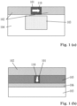
- FIG. 1 shows cross-sectional views illustrating examples of a nonlinear elements, more specifically the terahertz antenna arms forming the plasmonic slot waveguide for the propagation of optical signals.
- the cross-section is taken from the transverse plane of waveguide propagation.
- FIG. 1 (a) illustrates structured nonlinear material 101 with two metal electrodes 102 forming a plasmonic slot, and providing conductive material for the terahertz antenna.
- a (second) photonic waveguide 103 buried in the substrate 104 provides an access waveguide for optical pump signals.
- Light propagating in the higher refractive index material defining the photonic waveguide 103 is evanescently coupled to the plasmonic slot waveguide.
- the optical energy now propagates as surface plasmon polaritons (SPP) at the metal-insulator-metal interface.
- SPP surface plasmon polaritons
- the electric field of the propagating plasmonic mode is symbolized by an arrow 110.
- the plasmonic nature of the slot waveguide provides extreme sub-diffraction confinement of the optical field allowing an electrode spacing on the order of 100nm. This strong confinement of the optical pump signals leads to very strong optical intensities, essential for strong nonlinear effects.
- a terahertz wave incident onto the antenna results in a voltage across the two electrodes 102, and thus the antenna arms.
- This voltage across the nano-scale antenna gap leads to very strong terahertz electric fields in the nonlinear material 101 with same polarization orientation as an optical probe signal propagating along the plasmonic waveguide 110.
- the almost perfect overlap between the optical and the terahertz electric fields, and the strong field enhancement provided by the nano-scale slot result in a very strong and efficient nonlinear interaction between the optical and terahertz signals in the nonlinear material for terahertz wave detection.
- This implementation provides an efficient way to map the information contained in the terahertz on an optical carrier, providing an efficient terahertz wave detection.
- FIG. 1 (b) illustrates a vertical metal-insulator-metal waveguide.
- a bottom conductive electrode 106 such as a metal, a semimetal or transparent conductive oxide (TCO) is deposited on a substrate 103.
- the nonlinear material 101 on top of the first electrode can be structured, e.g. nanorods, or simply a thin fil. In case of a structured nonlinear material 101, an insulating layer 105 can be present present present.
- the top electrode 102 is acting as a top cladding. In such a vertical MIM waveguide, coupled/in light would propagate as SPP confined between the top and bottom electrodes.
- FIG. 2 illustrates a perspective view of an example of a terahertz detection and generation device comprising of a plasmonic waveguide and a terahertz antenna.
- the plasmonic waveguide is a metal-insulator-metal (MIM) slot waveguide formed by the antenna arms 201 and the nonlinear material as the core 202, present on a substrate 203.
- the metal can be either a metal or a semimetal.
- the antenna comprises two antenna arms 201 in form of four-clover-leave shape. Many other possible antenna shapes would work similarly, e.g. Bow-Tie and Yagi-Uda antennas.
- the core material 202 is a e.g. a second order nonlinear ferroelectric material, polymer or crystal.
- the nonlinear material could also rely on a third order nonlinear effect.
- Excited surface plasmon polaritons (SPP) propagating along the MIM slot waveguide are strongly confined inside of the plasmonic waveguide, leading to very high optical intensities in the nonlinear material.
- Two propagating SPP in the plasmonic slot result in generation of sum- and difference-frequency signals.
- Of interest for terahertz generation is mainly the difference-frequency generation (DFG) of two SPP with optical frequency SPP.
- DFG difference-frequency generation
- the resulting terahertz field is efficiently radiated in the far field by the terahertz antenna. This implementation would act as an efficient terahertz wave generation device.
- a terahertz wave incident on the antenna induces an oscillating current in the conductive antenna arms. Electrical charges accumulate at the antenna gap, resulting in a voltage across the slot. The voltage across the nano-scale slot results in a very strong terahertz electric field in the nonlinear material 202.
- the resonant nature of the antenna additionally enhances the terahertz electric field in the nonlinear material.
- the resulting terahertz electric field in the nonlinear material can interact with a propagating SPP of optical frequencies, and translate the information carried by the incident terahertz wave to the optical signal by means of sum-frequency generation.
- FIG. 3 shows cross-sectional illustrations of possible coupling schemes between free-space electromagnetic waves, in particular infrared, visible or ultra-violet light, and the first waveguide, i.e. the plasmonic waveguide.
- FIG. 3 (a) illustrates one embodiment in which the top silicon layer of a silicon-on-insulator (SOI) wafer 301 is selectively etched to pattern (second) photonic waveguides 302.
- This photonic waveguide is used to guide optical signals, e.g. coupled from a laser or fiber by means of grating coupler or edge coupling 303.
- the optical signal from the photonic waveguide couples to the plasmonic evanescently.
- the silicon waveguide 302 is tapered down to enhance the coupling efficiency from the photonic waveguide to the metal-insulator-metal (MIM) interface formed by the terahertz antenna arms 304 and the core 305 comprising the nonlinear material, i.e.
- MIM metal-insulator-metal
- FIG. 3 (b) illustrates an efficient coupling scheme between a free-space optical signal 307, and a plasmonic slot waveguide 305, by means of a diffractive optical element 308.
- the optical element is in close proximity with the plasmonic slot waveguide and structured in form of a focusing grating made of silicon.
- a free-space optical signal is diffracted by the grating and focused towards the plasmonic slot.
- the optical signal is evanescently coupled to the metal-insulator-metal interfaces. This provides an efficient scheme for coupling free-space electromagnetic waves in (307) and out (309) of the plasmonic waveguide.
- FIG. 4 shows an implementation example of a terahertz detector with an integrated Mach-Zehnder interferometer. This enables direct translation of the terahertz information to an amplitude modulation of an optical carrier signal (probe signal).
- the optical signal guided by a silicon waveguide 401 is split in two path, e.g. by a Y-splitter or multi-mode interferometer (MMI). Both silicon waveguide branches couple evanescently in close proximity with a (first) plasmonic waveguide.
- the plasmonic waveguide comprises the nonlinear material 402 and conductive electrodes, formed by portions of the antenna arms 403. The two inner electrodes interface both waveguide cores, thus functioning as claddings.
- the two antenna arms form the outer electrodes.
- An incident terahertz wave produces a voltage across both antenna gaps, which contain the nonlinear material 402.
- the terahertz electric field in the nonlinear material 402 changes the real part of the refractive index, thus inducing a phase shift of the optical signal (probe signal) proportional to the applied voltage.
- an opposite bias voltage between the outer and inner electrodes of the two plasmonic slot, an opposite phase shift can be induced.
- An induced ⁇ -phase shift difference between both plasmonic waveguides would result in destructive interference at the output combiner. This way one can modulate the intensity of the optical probe signal.
- Fig. 5 schematically illustrates a method for manufacturing a terahertz device.
- the first wafer comprises a layer of a nonlinear material (indicated in Fig. 5 as "Epi-ferroelectric), which can be, e.g., an epitaxially grown layer of a ferromagnetic material.
- the layer of nonlinear material is buried.
- possibly existing layers which are not required in the terahertz device are removed.
- the nonlinear material is structured so as to form a waveguide core (of a first - plasmonic - waveguide), and a layer of the second wafer is structure so as to form another waverguide core (of a second waveguide, such as a waveguide for probing and/or pumping).
- a layer of the second wafer is structure so as to form another waverguide core (of a second waveguide, such as a waveguide for probing and/or pumping).
- a second waveguide core of a second waveguide, such as a waveguide for probing and/or pumping.
- Electrodes are produced close to the first core, e.g., by selective metal deposition.
- the first wafer is made of the nonlinear material (possibly with an adhesion layer added).
- the core of the second waveguide from a layer of the second wafer, such as from the layer below the (optional) adhesion layer, such as from the layer indicated "Si" in Fig. 5 .
Description
- The invention relates to nonlinear elements in which terahertz (THz) frequency electromagnetic waves interact with nonlinear material systems, and to terahertz waves' detection and generation comprising the same. It relates to nonlinear elements, and devices enabling the mapping of a terahertz wave onto an optical frequency carrier, and an optical signal to produce a terahertz signal. The invention relates further to methods and apparatuses. The devices may find applications, e.g. in terahertz generation and terahertz sensing, terahertz imaging, terahertz communication and terahertz storage.
- Terahertz waves, a part of the electromagnetic spectrum unexplored until a decade ago has attracted a lot of attention in recent years. Terahertz waves provide several advantages due to their short wavelength providing a strong advantage compared to microwave imaging, transparent property to a lot of materials, and strong sensitivity to a phase change of the material system. In addition, material systems can respond strongly to terahertz radiation due to molecular vibrational modes, or optical phonon vibrations in crystals. Therefore, strong interest in the science community to find low-cost, power efficient and compact terahertz devices for generation and detection of terahertz waves has driven the terahertz technology. An important step towards low-cost, power efficient and compact foot-print, is the chip-scale integration of such devices for terahertz wave detection and generation. Especially, of interest is a device implementation that can perform both, detection and generation, only by changing the optical signal from probe to pump signal.
- So far, quite a few terahertz detection or generation technologies are related in one or the other way to the one of the two following approaches. Nonlinear terahertz generation and detection is achieved by using the second order nonlinearity of a nonlinear crystal, i.e. ZnTe, GaAs etc. A short optical pulse, referred to as the pump signal and inherently broadband, propagating through such a nonlinear crystal produces terahertz radiation through self-mixing of all its frequency components. For detection of such a produced terahertz wave, the pump signal is split and used as a probe signal to co-propagate through a similar nonlinear crystal along with the terahertz wave to be detected. The produced electric field in the crystal by the terahertz wave induces birefringence in the crystal changing the refractive index for one polarization of the crystal. This induces a polarization rotation to the optical pump signal. By reading out the polarization rotation of the optical probe signal by means of optoelectronic conversion, one can deduce the amplitude of the terahertz field present in the crystal. Another technique to generate and detect terahertz signals is based on photoconductive antennas. An incident optical pump signal on a high mobility substrate, i.e. GaAs, produces charge carriers. In the presence of a strong electric field, these carriers separate rapidly, and their acceleration produces terahertz waves. The use of metallic antenna arms to collect the generated carriers and to increase the radiation efficiency of the produced terahertz signal has shown efficient terahertz generation. For detection, similar as for nonlinear detection, the optical pump is split and used to probe the terahertz signal in a high mobility semiconductor. When a terahertz field is incident on the antenna, producing an electric field between its arms, the generated charge carrier by the optical pump drift apart generating a current which can be read and related to the terahertz field amplitude. One major drawback of those terahertz systems is the necessity to have both signals, i.e. optical pump and terahertz wave, coherent for time and frequency spectroscopy. In addition, a multitude of different approaches for the generation of terahertz waves have been demonstrated. However, all these approaches are very costly and bulky, and require complex free space optical systems. Plasmonics has in recent years been used to enhance terahertz detection and generation, enabling smaller and more efficient devices. The combination of plasmonics with nonlinear crystals on a chip-scale integrated structure, remains a challenge.
-
US 2008/0159342 A1 pertains to terahertz radiation sources having a dual waveguide structure that incorporates both an optical waveguide and a terahertz waveguide. More precisely, the THz radiation source includes an optical waveguide contained within a larger THz waveguide layered structure and it provides a coherent guided wave of THz radiation. -
WO 2016/154764 A2 discloses devices for enabling optical phase, amplitude and intensity modulation. The devices are configured to modulate light in the infrared and/or in the visible and/or in the ultraviolet range and for applications such as optical data- and telecommunication, optical storage and optical sensing. The devices are able to modulate an optical phase by comprising a first waveguide and first and second electrodes. The first waveguide comprises a core of ferroelectric material. The first and second electrodes are arranged in a manner to produce an electric field in the ferroelectric material when a voltage is applied between the first and second electrodes. The electric field modulates at least the real part of the refractive index of the ferroelectric material and hence modulates the phases of the plasmon polariton modes present at the interface between the core (ferroelectric material) and its cladding. - M. Brula et al., "Microwave Plasmonics: A Novel Platform for RF Photonics," IEEE International Topical Meeting on Microwave Photonics 2016, pp. 259-262 discusses the potential of the plasmonic platform, this means of surface plasmon polaritons, for microwave photonics applications, in particular for plasmonic organic hybrid modulators. D1 discloses plasmonic-photonic Mach-Zehnder Modulators (MZMs), all-plasmonic MZMs and IQ modulators, Plasmonic Phase Modulators (PPMs) co-integrated with antennas, and plasmonic beamforming networks.
- Y. Salamin et al., "Direct Conversion of Free Space Millimeter Waves to Optical Domain by Plasmonic Modulator Antenna," Nano Lett., vol. 15, no. 12, pp. 8342-8346, 2015 and Y. Salamin et al., "Direct RF-to-Optical Detection by Plasmonic modulator integrated into a four-lea-clover antenna," OSA Tech. Digest (2016), p. SM1E.6 discuss in detail the devices disclosed in Burla et al. that comprise a PPM that is co-integrated with an antenna. The devices comprise a plasmonic organic phase modulator that comprises a single metal-insulator-metal (MIM) slot waveguide, wherein the slot is filled with a nonlinear organic material, and that is co-integrated with an antenna, in particular a four-clover-leaf antenna or a bowtie antenna. The devices comprise further a straight, non-splitting photonic waveguide that is arranged on the same plane as the MIM slot waveguide.
-
WO 2004/097382 A1 relates to a THz emission source for use in the field of medical technology, in particular for in-vivo use. The THz emission source comprises a source device, a guide and a miniature emission head. The source device emits two waves that differ in frequency in the order of THz. The guide is realized as an optical fiber that is configured to convey the waves to the detection surface of a photodetector arranged in the miniature emission head. The photodetector used comprises a nonlinear material and is configured to generate the difference frequency of the two waves. The miniature emission head comprises further an antenna configured to emit the generated difference frequency. - Possible objects of the invention are one or more of
- to enable light modulation by terahertz waves;
- to provide plasmonic or plasmonic-hybrid waveguides of high nonlinear conversion efficiency
- to provide plasmonic or plasmonic-hybrid waveguide of small size;
- to enable efficient terahertz wave detection and generation;
- to integrate terahertz wave devices in standard semiconductor manufacturing processes, in particular in CMOS technology or in Micro-Electro-Mechanical System Technology or in Memory Technology;
- Further objects and various advantages emerge from the description and embodiments below.
- At least one of these objects is at least partially achieved by devices according to the patent claims.
- For example, the device (sometimes referred to as "element") in which terahertz waves interact with light comprises a first antenna which is a terahertz wave antenna featuring a nonlinear material loaded plasmonic slot waveguide comprising
- a first core comprising a nonlinear material; and
- a cladding comprising a first cladding portion comprising, at a first interface with the nonlinear material such as the ferroelectric material, a first cladding material having a high conductivity such as in a metal or semimetal or a highly doped semiconductor;
- In instances, the nonlinear materials, and in particular the ferroelectric material can be grown, in particular epitaxially grown, on the substrate wafer, with zero or one or more intermediate layers present between the substrate and the ferroelectric materials, wherein the one or more intermediate layers, if present, are e.g. spin coated, sputtered or grown, in particular epitaxially or solution grown, on the substrate, the substrate and the first core being stacked in a direction referred to as vertical direction, and directions perpendicular to the vertical direction are referred to as lateral directions.
- In one embodiment, the substrate is made of a ferroelectric material. In particular, the substrate can be made of the same ferroelectric material as the ferroelectric material comprised in the first core. E.g., both, the ferroelectric material comprised in the first core and the ferroelectric material of the substrate, can be LiNbO3, or BaTiO3, or (1-x)[Pb(Mg1/3Nb2/3O3]-x[PbTiO3] (with the same x); but other ferroelectric materials can be used, too. It can in particular be provided in such an embodiment, that no intermediate layer is present between the substrate and the ferroelectric material of the core.
- In one embodiment, the substrate and the ferroelectric material comprised in the first core are different portions of one and the same ferroelectric single crystal, e.g., of one and the same crystal of LiNbO3, or BaTiO3, or (1-x)[Pb(Mg1/3Nb2/3O3]-x[PbTiO3]. Said ferroelectric single crystal, being a unitary part, can provide in such an embodiment, that no intermediate layer is present between the substrate and the ferroelectric material of the core.
- In one embodiment, the antenna comprises of two arms, the antenna gap forming the plasmonic slot filled with the nonlinear material.
- In one embodiment, a second waveguide which is provided for guiding photonic, or plasmonic, or plasmonic hybrid modes along propagation directions can be present and typically manufactured on the same substrate wafer comprising the nonlinear (for example ferroelectric) materials. The second waveguide can be made of any material of the substrate wafer, including the ferroelectric material.
- In an alternative, the aforementioned second waveguide can also be present on a second substrate wafer different from the substrate wafer comprising the nonlinear material. Coupling, e.g. evanescent coupling and/or butt coupling, between the second waveguide and the core of the first waveguide consisting of the nonlinear material is usually present when the photonic, or plasmonic, or plasmonic hybrid modes propagate in the second waveguide. The said two substrate wafers may require being in close proximity to each other accomplished, e.g., by means of wafer bonding technique, including direct bonding technique or adhesive bonding technique which requires an adhesion layer.
- The nonlinear materials used for interacting with terahertz wave can in particular be ferroelectric materials. The ferroelectric material could be any one, such as LiNbO3, KNO3, KTaxNb1-xO3, BaxSr1-xTiO3, SrBaNbO3, K3Li2Nb5O15, KxNa1-xSryBa1-y-Nb2O6, KH2PO4, KH2AsO4, NH4H2PO4, ND4D2PO4, RbH2AsO4, KTiOPO4, KTiOAsO4, RbTiOPOa, RbTiOAsO4, CsTiOAsO4, Pb(ZrxTi1-x)O3, La-doped Pb(ZrxTi1-x)O3, (1-x)[Pb(Mg1/3Nb2/3O3)-x[PbTiO3], or (1-x)[Pb(Zn1/3Nb2/3O3)-x[PbTiO3], (0<x<1; 0<y<1), but is not limited thereto. Also, ferroelectric materials can be synthetized artificially, based on non-ferroelectric materials. Moreover, ferroelectric materials are not necessarily in their phases exhibiting ferroelectricity but can be in any phases, provided that the materials exhibit the desired nonlinear effects. The metallic materials for electrodes and conductive claddings, respectively, can be Au, Ag, Pt, Al, Cu, W, and Ti, but are not limited to these aforementioned metals; preferably CMOS process-compatible metals such as Cu or W can be used. If a non-metallic electrically conductive material is used (e.g, as the material of the second electrode), it may be a conductive oxide such as SrRuO3, LaSrCoOs, LaNiO3, indium tin oxide, or other conductive materials such as graphene, but it is not limited thereto. Non-metallic electrically conductive materials can be used as interfacial materials (cladding) at the ferroelectric material (core) to reduce leakage currents through the ferroelectric material.
- Light to be modulated or used for the generation and detection of terahertz wave can in particular be infrared light, but more generally can be any electromagnetic radiation, in particular light in the infrared and/or in the visible and/or in the ultraviolet range.
- In particular, a terahertz device according to the claimed invention comprises a first waveguide which is a plasmonic waveguide comprising
- a first core comprising a nonlinear material, in particular a ferroelectric material; and
- a cladding comprising a first cladding portion comprising, at a first interface with the first core, in particular with the nonlinear material, a first cladding material which is an electrically conductive material.
- And the terahertz device comprises further
- an antenna having a first and a second arm (for receiving or for emitting or for both, receiving and emitting electromagnetic waves in the terahertz range);
- a first and a second electrode arranged close to the first waveguide.
- The terahertz device can be a device for detecting electromagnetic waves in the terahertz range.
- In some embodiments, the terahertz device is a device for emitting electromagnetic waves in the terahertz range.
- In some embodiments, the terahertz device is a device for for both, detecting and emitting electromagnetic waves in the terahertz range.
- Under "terahertz range", we understand, as is common, the frequency range from 0.1 THz to 10 THz, or more particularly from 0.3 THz to 10 THz.
- The non-linear material is, more specifically, a material which has a non-linear polarization response (in the respective frequency range, such as instantly in the optical range).
- In some embodiments, the non-linear material is an electrically insulating material.
- But alternatively, it can also be an electrically conductive material, wherein in that case, the core can comprise an electrically insulating material arranged between the nonlinear material and the cladding.
- The nonlinear material can be a single-crystalline material. But it can also be an amorphous material, or it can be a nanostructured material.
- In some embodiments, the nonlinear material is a single-crystalline material.
- In some embodiments, the nonlinear material is a polycrystalline material/ single crystalline
- In some embodiments, the nonlinear material is a ferroelectric single crystal.
- The first cladding material can be a material having a permittivity having a negative real part (in the THz range).
- The first cladding material can be metallic or a semi-metallic, e.g., can be a highly doped semiconductor.
- The first and second arms can be distinct from and electrically connected to or identical with the first and the second electrodes, respectively.
- The terms "lateral" and "vertical" as used in the present patent application refer to the wafer which is a substantially disk- or plate-like shaped item having in one direction (vertical direction) an extension (thickness) which is small with respect to its extension in the other two directions (lateral directions).
- The device according to the claimed invention comprises, in addition, a second waveguide that is a photonic waveguied comprising a second core positioned in proximity to the first waveguide, for enabling coupling (e.g., an evanescent coupling) between the first and second waveguides.
- Alternatively, although not covered by the claimed invention, the second waveguide can also be a plasmonic waveguide, or it can be a plasmonic-photonic hybride waveguide.
- The second waveguide can be used to guide and couple to the first waveguide, so as to provide and to receive a probe signal in case terahertz electromagnetic waves are detected using the device, or, in case the device is used to generate terahertz electromagnetic waves, so as to provide a pump signal to the first waveguide, such as a pump signal comprising pulses or a pump signal comprising two or more optical frequencies. Due to the non-linearity of the nonlinear material, the two or more frequencies can be transformed (by the first waveguide) to comprise a sum and (rather) a difference frequency which is in the terahertz range.
- At least one of the following applies for the device according to the claimed invention:
- The second waveguide is arranged vertically between the substrate and the first waveguide.
- The second waveguide is buried in the substrate.
- The device comprises an integrated Mach-Zehnder interferometer by the second waveguide (401) being split in two branches, wherein both branches are arranged to couple evanescently in close proximity with a first waveguide, wherein the device comprises two inner electrodes that function as cladings and two outer electrodes formed by the
antenna arms 403. - In an embodiment, the device may comprise a substrate comprising one or more substrate layers, wherein both, the first and the second waveguide, are located on and attached to the substrate.
- In some embodiments, the device comprises an optical structure, in particular a diffractive optical structure, for enhancing a coupling between free-space electromagnetic waves (such as free-space electromagnetic waves in the infrared, in the visible or in the ultraviolet range) and the first waveguide. E.g., the optical structure can be a focusing optical structure. For example, pump signals can be efficiently provided to the first waveguide.
- The optical structure may be provided for focusing the free-space exelctromagnetic waves into an end of the first waveguide.
- Alternatively or in addition, the optical strucutre may comprise a first part and a second part, for enhancing a coupling of free-space electromagnetic waves to a first end and to a second end, respectively, of the first waveguide.
- Alternatively or in addition, the optical structure may be an optical structure exhibiting a variation of optical properties, in particular of a refractive index, on distances below 100 micrometers, in particular on distances between 10 micrometers and 0.01 micrometers.
- Manufacturing the above or other terahertz devices can be accomplished using a technique with wafer bonding. A first wafer is bonded to a second wafer, wherein the nonlinear material is comprised in the first wafer. The first wafer can be made of the nonlinear material or, in other embodiments, can comprise the nonlinear material and, in addition, one or more further layers of other material.
- E.g., the method for manufacturing a terahertz device (which can be, e.g., a device as herein described) can in particular comprise:
- providing a first wafer, such as a silicon-on-insulator wafer or a single-crystalline silicon wafer;
- depositing on the first wafer a nonlinear material, in particular a ferroelectric material;
- providing a second wafer, such as a silicon-on-insulator wafer or a single-crystalline silicon wafer, optionally with an adhesion layer;
- bonding the first wafer to the second wafer, so as to obtain a stacked wafer, thereby burying the nonlinear material, e.g., such that the nonlinear material interfaces the second wafer.
- The depositing can be accomplished (e.g., epitaxially), for example by laser ablation, molecular beam epitaxy, sputtering or other vacuum deposition techniques.
- Or, e.g., the method for manufacturing a terahertz device (which can be, e.g., a device as herein described) can in particular comprise:
- providing a first wafer made of a nonlinear material, in particular of a ferroelectric material, optionally with an adhesion layer;
- providing a second wafer, such as a silicon-on-insulator wafer or a single-crystalline silicon wafer, optionally with an adhesion layer;
- bonding the first wafer to the second wafer, so as to obtain a stacked wafer.
- The invention comprises devices with features of corresponding methods according to the invention, and, vice versa, also methods with features of corresponding devices according to the invention. However, the methods are not covered by the claimed invention.
- The advantages of the devices basically correspond to the advantages of corresponding methods, and, vice versa, the advantages of the methods basically correspond to the advantages of corresponding devices.
- Further embodiments and advantages emerge from the following description and the enclosed figures and from the dependent claims.
- Below, the invention is described in more detail by means of examples and the included drawings. In the drawings, same reference numerals refer to same or analogous elements. The figures show schematically:
-
FIG. 1 (a) and FIG. 1 (b) are a cross sectional view of examples of nonlinear elements. It illustrates a nonlinear element loaded terahertz wave antenna gap forming a metal-insulator-metal plasmonic slot waveguide based on ferroelectric material. -
FIG. 2 illustrates a perspective view of an example of a terahertz detection and generation device comprising of a plasmonic waveguide and a terahertz antenna. -
FIG. 3 (a) and FIG. 3 (b) show cross-sectional illustrations of possible coupling schemes between free-space electromagnetic waves and the first waveguide, i.e. the plasmonic waveguide. The embodiment according toFig. 3 (b) is not covered by the claimed invention. -
FIG. 4 shows an implementation example of a terahertz detector with an integrated Mach-Zehnder interferometer. -
Fig. 5 schematically illustrates a method for manufacturing a terahertz device, wherein the method is not covered by the claimed invention. - The described embodiments are meant as examples or for clarifying the invention and shall not limit the invention.
-
FIG. 1 shows cross-sectional views illustrating examples of a nonlinear elements, more specifically the terahertz antenna arms forming the plasmonic slot waveguide for the propagation of optical signals. The cross-section is taken from the transverse plane of waveguide propagation. -
FIG. 1 (a) illustrates structurednonlinear material 101 with twometal electrodes 102 forming a plasmonic slot, and providing conductive material for the terahertz antenna. A (second)photonic waveguide 103 buried in thesubstrate 104 provides an access waveguide for optical pump signals. Light propagating in the higher refractive index material defining thephotonic waveguide 103, is evanescently coupled to the plasmonic slot waveguide. The optical energy now propagates as surface plasmon polaritons (SPP) at the metal-insulator-metal interface. The electric field of the propagating plasmonic mode is symbolized by anarrow 110. The plasmonic nature of the slot waveguide provides extreme sub-diffraction confinement of the optical field allowing an electrode spacing on the order of 100nm. This strong confinement of the optical pump signals leads to very strong optical intensities, essential for strong nonlinear effects. - When two optical pump signals co-propagate along the nonlinear material loaded plasmonic waveguide, strong second order nonlinear interaction between the two optical pump signals result in sum and difference frequency generation. If the two carriers are non-equal, the resulting new signal from the difference frequency generation is equal to the relative frequency offset of the two optical pump signals. This offset can be set to the desired terahertz frequency. The resulting terahertz field leads to charge oscillation in the electrodes resulting in an oscillating current in the conductive electrodes and efficient radiation in the far field by the terahertz antenna. In another instance, the nonlinear third order effect may be exploited to generate a terahertz signal by means of fourwave mixing. These implementations can act as an efficient terahertz wave generation device.
- On the other hand, a terahertz wave incident onto the antenna results in a voltage across the two
electrodes 102, and thus the antenna arms. This voltage across the nano-scale antenna gap leads to very strong terahertz electric fields in thenonlinear material 101 with same polarization orientation as an optical probe signal propagating along theplasmonic waveguide 110. The almost perfect overlap between the optical and the terahertz electric fields, and the strong field enhancement provided by the nano-scale slot, result in a very strong and efficient nonlinear interaction between the optical and terahertz signals in the nonlinear material for terahertz wave detection. This implementation provides an efficient way to map the information contained in the terahertz on an optical carrier, providing an efficient terahertz wave detection. -
FIG. 1 (b) illustrates a vertical metal-insulator-metal waveguide. A bottomconductive electrode 106 such as a metal, a semimetal or transparent conductive oxide (TCO) is deposited on asubstrate 103. Thenonlinear material 101 on top of the first electrode can be structured, e.g. nanorods, or simply a thin fil. In case of a structurednonlinear material 101, an insulatinglayer 105 can be present present. Thetop electrode 102 is acting as a top cladding. In such a vertical MIM waveguide, coupled/in light would propagate as SPP confined between the top and bottom electrodes. Choosing adielectric cladding 105 with a smaller refractive index as thenonlinear material 101, gives additionally a horizontal confinement. The electric field of the SPP are polarized in the vertical direction as shown by thearrow 110. Such a structure would provide a very strong sub-wavelength confinement of optical signals, resulting in strong nonlinear interactions in the nonlinear material. -
FIG. 2 illustrates a perspective view of an example of a terahertz detection and generation device comprising of a plasmonic waveguide and a terahertz antenna. The plasmonic waveguide is a metal-insulator-metal (MIM) slot waveguide formed by theantenna arms 201 and the nonlinear material as thecore 202, present on asubstrate 203. The metal can be either a metal or a semimetal. The antenna comprises twoantenna arms 201 in form of four-clover-leave shape. Many other possible antenna shapes would work similarly, e.g. Bow-Tie and Yagi-Uda antennas. Thecore material 202 is a e.g. a second order nonlinear ferroelectric material, polymer or crystal. The nonlinear material could also rely on a third order nonlinear effect. Excited surface plasmon polaritons (SPP) propagating along the MIM slot waveguide are strongly confined inside of the plasmonic waveguide, leading to very high optical intensities in the nonlinear material. Two propagating SPP in the plasmonic slot result in generation of sum- and difference-frequency signals. Of interest for terahertz generation is mainly the difference-frequency generation (DFG) of two SPP with optical frequency SPP. The resulting terahertz field is efficiently radiated in the far field by the terahertz antenna. This implementation would act as an efficient terahertz wave generation device. - A terahertz wave incident on the antenna induces an oscillating current in the conductive antenna arms. Electrical charges accumulate at the antenna gap, resulting in a voltage across the slot. The voltage across the nano-scale slot results in a very strong terahertz electric field in the
nonlinear material 202. In addition, the resonant nature of the antenna additionally enhances the terahertz electric field in the nonlinear material. The resulting terahertz electric field in the nonlinear material can interact with a propagating SPP of optical frequencies, and translate the information carried by the incident terahertz wave to the optical signal by means of sum-frequency generation. -
FIG. 3 shows cross-sectional illustrations of possible coupling schemes between free-space electromagnetic waves, in particular infrared, visible or ultra-violet light, and the first waveguide, i.e. the plasmonic waveguide. -
FIG. 3 (a) illustrates one embodiment in which the top silicon layer of a silicon-on-insulator (SOI)wafer 301 is selectively etched to pattern (second)photonic waveguides 302. This photonic waveguide is used to guide optical signals, e.g. coupled from a laser or fiber by means of grating coupler oredge coupling 303. In proximity to the plasmoinc waveguide, the optical signal from the photonic waveguide couples to the plasmonic evanescently. In addition, thesilicon waveguide 302 is tapered down to enhance the coupling efficiency from the photonic waveguide to the metal-insulator-metal (MIM) interface formed by theterahertz antenna arms 304 and thecore 305 comprising the nonlinear material, i.e. formed by plasmonic waveguide. These SPP strongly confined to thenonlinear material 305 propagate along the MIM slot waveguide, providing, as described forFIG. 1 , strong nonlinear interaction between propagating SPP and terahertz field. The propagating SPP, can evanescently couple back to the photonic waveguide at the end of the plasmonic waveguide. These optical signals can be coupled out to a fiber orcamera 306 for temporal or spectral analysis. -
FIG. 3 (b) illustrates an efficient coupling scheme between a free-spaceoptical signal 307, and aplasmonic slot waveguide 305, by means of a diffractiveoptical element 308. In this embodiment, the optical element is in close proximity with the plasmonic slot waveguide and structured in form of a focusing grating made of silicon. A free-space optical signal is diffracted by the grating and focused towards the plasmonic slot. At the edges of the optical element, the optical signal is evanescently coupled to the metal-insulator-metal interfaces. This provides an efficient scheme for coupling free-space electromagnetic waves in (307) and out (309) of the plasmonic waveguide. -
FIG. 4 shows an implementation example of a terahertz detector with an integrated Mach-Zehnder interferometer. This enables direct translation of the terahertz information to an amplitude modulation of an optical carrier signal (probe signal). In this embodiment, the optical signal guided by asilicon waveguide 401 is split in two path, e.g. by a Y-splitter or multi-mode interferometer (MMI). Both silicon waveguide branches couple evanescently in close proximity with a (first) plasmonic waveguide. The plasmonic waveguide comprises thenonlinear material 402 and conductive electrodes, formed by portions of theantenna arms 403. The two inner electrodes interface both waveguide cores, thus functioning as claddings. The two antenna arms form the outer electrodes. An incident terahertz wave produces a voltage across both antenna gaps, which contain thenonlinear material 402. The terahertz electric field in thenonlinear material 402 changes the real part of the refractive index, thus inducing a phase shift of the optical signal (probe signal) proportional to the applied voltage. By applying an opposite bias voltage between the outer and inner electrodes of the two plasmonic slot, an opposite phase shift can be induced. An induced π-phase shift difference between both plasmonic waveguides would result in destructive interference at the output combiner. This way one can modulate the intensity of the optical probe signal. -
Fig. 5 schematically illustrates a method for manufacturing a terahertz device. Two wafers are bonded to each other, wherein the first wafer comprises a layer of a nonlinear material (indicated inFig. 5 as "Epi-ferroelectric), which can be, e.g., an epitaxially grown layer of a ferromagnetic material. In the obtained wafer (referred to as stacked wafer), the layer of nonlinear material is buried. In a next step, possibly existing layers which are not required in the terahertz device are removed. - In further steps, the nonlinear material is structured so as to form a waveguide core (of a first - plasmonic - waveguide), and a layer of the second wafer is structure so as to form another waverguide core (of a second waveguide, such as a waveguide for probing and/or pumping). Alternatively to forming the second core from a layer of the second wafer, it is also possible to deposit further material on the stacked wafer and to produce the second core from that further material.
- Electrodes are produced close to the first core, e.g., by selective metal deposition.
- In an alternative method, the first wafer is made of the nonlinear material (possibly with an adhesion layer added). In that case, it is possible to structure the core of the second waveguide from a layer of the second wafer, such as from the layer below the (optional) adhesion layer, such as from the layer indicated "Si" in
Fig. 5 .
Claims (10)
- A terahertz device for detecting or for emitting or for both, detecting and emitting electromagnetic waves in the terahertz range, the device comprising on a substrate a first waveguide which is a plasmonic waveguide comprising- a first core comprising a nonlinear material (101, 202, 305, 402), in particular a ferroelectric material; and- a cladding comprising a first cladding portion comprising, at a first interface with the first core, in particular with the nonlinear material, a first cladding material which is an electrically conductive material;the device comprising a first and a second electrode (102) arranged close to the first waveguide,wherein the device comprises an antenna having a first and a second arm (201, 304, 403), for receiving or for emitting or for both, receiving and emitting electromagnetic waves in the terahertz range,wherein the device comprises a second waveguide (103, 302, 401), wherein the second waveguide is a photonic waveguide comprising a second core positioned in proximity to the first waveguide, for enabling coupling between the first and second waveguides,characterized in that- the second waveguide is arranged vertically between the substrate (104, 203, 301) and the first waveguide; and/or- the second waveguide is buried in the substrate; and/or- the device comprises an integrated Mach-Zehnder interferometer by the second waveguide (401) being split in two branches, wherein both branches are arranged to couple evanescently in close proximity with a first waveguide, wherein the device comprises two inner electrodes that function as cladings and two outer electrodes formed by the antenna arms 403.
- The device according to claim 1, wherein the device is a terahertz emitter for emitting electromagnetic waves in the terahertz range, and wherein the first and second electrodes (102) are provided for picking up an electric field present in the nonlinear material (101, 202, 305, 402).
- The device according to claim 1, wherein the device is a terahertz detector for detecting electromagnetic waves in the terahertz range, and wherein the first and second electrodes (102) are provided for producing an electric field in the nonlinear material (101, 202, 305, 402) when a voltage is applied between the first and second electrodes, for modulating an optical property of the nonlinear material, such as for modulating at least a real part of a refractive index of the nonlinear material.
- The device according to one of claims 1 to 3, wherein the first electrode establishes the first cladding portion, in particular wherein the first cladding material is a metallic material.
- The device according to one of claims 1 to 4, wherein the cladding comprises a second cladding portion separate from the first cladding portion, comprising, at a second interface with the ferroelectric material, a second cladding material which is an electrically conductive material.
- The device according to claim 5, wherein the nonlinear material (101, 202, 305, 402) is arranged, in particular laterally arranged, between the first and second cladding portions, in particular wherein the first electrode establishes the first cladding portion and the second electrode establishes the second cladding portion.
- The device according to one of claims 1 to 6, wherein the enabled coupling is evanescent coupling.
- The device according to one of claims 1 to 7, comprising an optical structure, in particular a diffractive optical structure (308), for enhancing a coupling between free-space electromagnetic waves, in particular free-space electromagnetic waves in the infrared, in the visible or in the ultraviolet range, and the first waveguide, in particular wherein the optical structure is a focusing optical structure.
- The device according to one of claims 1-8, wherein the nonlinear material is a single-crystalline material, a polycristalline material or a nanostructured material.
- The device according to one of claims 1-8, wherein the nonlinear material is an amorphous material.
Applications Claiming Priority (2)
| Application Number | Priority Date | Filing Date | Title |
|---|---|---|---|
| CH3742017 | 2017-03-21 | ||
| PCT/EP2018/056925 WO2018172302A1 (en) | 2017-03-21 | 2018-03-20 | DEVICE FOR THz GENERATION AND/OR DETECTION AND METHODS FOR MANUFACTURING THE SAME |
Publications (2)
| Publication Number | Publication Date |
|---|---|
| EP3602188A1 EP3602188A1 (en) | 2020-02-05 |
| EP3602188B1 true EP3602188B1 (en) | 2023-07-12 |
Family
ID=61750120
Family Applications (1)
| Application Number | Title | Priority Date | Filing Date |
|---|---|---|---|
| EP18712572.9A Active EP3602188B1 (en) | 2017-03-21 | 2018-03-20 | Device for thz generation and/or detection and methods for manufacturing the same |
Country Status (5)
| Country | Link |
|---|---|
| US (1) | US11499915B2 (en) |
| EP (1) | EP3602188B1 (en) |
| JP (1) | JP7194444B2 (en) |
| CA (1) | CA3053333A1 (en) |
| WO (1) | WO2018172302A1 (en) |
Families Citing this family (6)
| Publication number | Priority date | Publication date | Assignee | Title |
|---|---|---|---|---|
| JP7226554B2 (en) * | 2019-07-24 | 2023-02-21 | 日本電信電話株式会社 | Plasmonic waveguide and manufacturing method thereof |
| EP4054074A1 (en) * | 2021-03-03 | 2022-09-07 | Terra Quantum AG | Terahertz ferroelectric resonator |
| CN113093330A (en) * | 2021-03-24 | 2021-07-09 | 深圳大学 | Nonlinear slit optical waveguide and preparation method and application thereof |
| CN113670848B (en) * | 2021-08-23 | 2022-08-02 | 中国人民解放军军事科学院国防科技创新研究院 | High-resolution broadband terahertz detector based on pixelized structure and detection method |
| WO2023153138A1 (en) * | 2022-02-14 | 2023-08-17 | ソニーグループ株式会社 | Wave control device, wavelength conversion element, computing element, sensor, polarization control element, and optical isolator |
| DE102022202028A1 (en) | 2022-02-28 | 2023-08-31 | Volkswagen Aktiengesellschaft | Radar sensor device for a vehicle, and radar system with a radar sensor device and vehicle with a radar system |
Citations (1)
| Publication number | Priority date | Publication date | Assignee | Title |
|---|---|---|---|---|
| FR2854504A1 (en) * | 2003-04-30 | 2004-11-05 | Thales Sa | TERAHERTZ TRANSMISSION SOURCE AND OPTICAL SYSTEM COMPRISING SUCH A SOURCE |
Family Cites Families (13)
| Publication number | Priority date | Publication date | Assignee | Title |
|---|---|---|---|---|
| US6967347B2 (en) * | 2001-05-21 | 2005-11-22 | The Regents Of The University Of Colorado | Terahertz interconnect system and applications |
| US7126151B2 (en) | 2001-05-21 | 2006-10-24 | The Regents Of The University Of Colorado, A Body Corporate | Interconnected high speed electron tunneling devices |
| US6914999B2 (en) * | 2002-05-31 | 2005-07-05 | Spectalis Corp. | Electro-optic modulators |
| JP4794878B2 (en) | 2004-03-26 | 2011-10-19 | キヤノン株式会社 | Photoconductive element |
| US7515801B2 (en) | 2006-12-28 | 2009-04-07 | Wisconsin Alumni Research Foundation | Coherent terahertz radiation source |
| JP5419411B2 (en) * | 2008-10-08 | 2014-02-19 | キヤノン株式会社 | Terahertz wave generator |
| JP5709562B2 (en) | 2010-03-04 | 2015-04-30 | キヤノン株式会社 | Terahertz wave generating element and terahertz time domain spectrometer |
| JP2014165412A (en) * | 2013-02-27 | 2014-09-08 | Seiko Epson Corp | Short optical pulse generation device, terahertz wave generation device, camera, imaging apparatus, and measuring device |
| JP2014207654A (en) | 2013-03-16 | 2014-10-30 | キヤノン株式会社 | Waveguide element |
| JP2015118244A (en) * | 2013-12-18 | 2015-06-25 | セイコーエプソン株式会社 | Short optical pulse generation device, terahertz wave generation device, camera, imaging device and measurement device |
| US9442314B2 (en) | 2014-08-12 | 2016-09-13 | Oracle International Corporation | Ferroelectric-enhanced tuning of ring resonators by using fields parallel to and above a top surface thereof |
| JP6096725B2 (en) * | 2014-09-09 | 2017-03-15 | アイシン精機株式会社 | Film thickness measuring apparatus and film thickness measuring method |
| CA3017237C (en) | 2015-04-01 | 2023-09-26 | Eth Zurich | Electrooptic modulator |
-
2018
- 2018-03-20 US US16/495,178 patent/US11499915B2/en active Active
- 2018-03-20 CA CA3053333A patent/CA3053333A1/en active Pending
- 2018-03-20 EP EP18712572.9A patent/EP3602188B1/en active Active
- 2018-03-20 WO PCT/EP2018/056925 patent/WO2018172302A1/en unknown
- 2018-03-20 JP JP2019552053A patent/JP7194444B2/en active Active
Patent Citations (1)
| Publication number | Priority date | Publication date | Assignee | Title |
|---|---|---|---|---|
| FR2854504A1 (en) * | 2003-04-30 | 2004-11-05 | Thales Sa | TERAHERTZ TRANSMISSION SOURCE AND OPTICAL SYSTEM COMPRISING SUCH A SOURCE |
Non-Patent Citations (3)
| Title |
|---|
| BURLA MAURIZIO ET AL: "Microwave plasmonics: A novel platform for RF photonics", 2016 IEEE INTERNATIONAL TOPICAL MEETING ON MICROWAVE PHOTONICS (MWP), IEEE, 31 October 2016 (2016-10-31), pages 259 - 262, XP033035759, DOI: 10.1109/MWP.2016.7791329 * |
| SALAMIN Y ET AL: "Direct RF-to-optical detection by plasmonic modulator integrated into a four-leaf-clover antenna", 2016 CONFERENCE ON LASERS AND ELECTRO-OPTICS (CLEO), OSA, 5 June 2016 (2016-06-05), pages 1 - 2, XP033025570 * |
| SALAMIN YANNICK ET AL: "Direct Conversion of Free Space Millimeter Waves to Optical Domain by Plasmonic Modulator Antenna", NANO LETTERS, vol. 15, no. 12, 19 November 2015 (2015-11-19), US, pages 8342 - 8346, XP055802104, ISSN: 1530-6984, DOI: 10.1021/acs.nanolett.5b04025 * |
Also Published As
| Publication number | Publication date |
|---|---|
| JP2020512585A (en) | 2020-04-23 |
| WO2018172302A1 (en) | 2018-09-27 |
| JP7194444B2 (en) | 2022-12-22 |
| US20200408677A1 (en) | 2020-12-31 |
| EP3602188A1 (en) | 2020-02-05 |
| CA3053333A1 (en) | 2018-09-27 |
| US11499915B2 (en) | 2022-11-15 |
Similar Documents
| Publication | Publication Date | Title |
|---|---|---|
| EP3602188B1 (en) | Device for thz generation and/or detection and methods for manufacturing the same | |
| CN107430297B (en) | Electro-optic modulator | |
| EP3691033B1 (en) | Optical phased array antenna and lidar including same | |
| US9599770B2 (en) | Graphene photonics for resonator-enhanced electro-optic devices and all-optical interactions | |
| US9304373B2 (en) | Terahertz wave generation element, terahertz wave detection element, and terahertz time domain spectroscope device | |
| US8311374B2 (en) | Beam generation and steering with integrated optical circuits for light detection and ranging | |
| US7783199B2 (en) | Frequency selective MMW source | |
| Olivieri et al. | Plasmonic nanostructured metal–oxide–semiconductor reflection modulators | |
| Berini | Optical beam steering using tunable metasurfaces | |
| CN109997056A (en) | The low cost and compact optical phased array turned to electric light beam arranges | |
| US20220326438A1 (en) | A plasmonic device enabling simplified fabrication | |
| US20110170820A1 (en) | Eo polymer-based dual slot waveguide modulators | |
| US10261390B2 (en) | Laser beam steering device and system including the same | |
| US8909002B2 (en) | Light modulator, optical pickup, and light modulation module | |
| Bavil et al. | Active unidirectional propagation of surface plasmons at subwavelength slits | |
| Edelstein et al. | Waveguide-integrated mid-IR photodetector and all-optical modulator based on interlayer excitons absorption in a WS2/HfS2 heterostructure | |
| US20080112705A1 (en) | Frequency selective mmw source | |
| US8780431B1 (en) | Plasmon absorption modulator systems and methods | |
| JP2012022159A (en) | Wavelength conversion element | |
| US11243419B2 (en) | Electro-optic silicon nitride via electric poling | |
| US7283704B2 (en) | Optical signal-electric signal converter | |
| Poon et al. | Silicon photonics for the visible and near-infrared spectrum | |
| US20230168561A1 (en) | Electro-optical modulators and applications based on silicon processing compatible nonlinear optical materials | |
| JPS6374028A (en) | Optical modulator |
Legal Events
| Date | Code | Title | Description |
|---|---|---|---|
| STAA | Information on the status of an ep patent application or granted ep patent |
Free format text: STATUS: UNKNOWN |
|
| STAA | Information on the status of an ep patent application or granted ep patent |
Free format text: STATUS: THE INTERNATIONAL PUBLICATION HAS BEEN MADE |
|
| PUAI | Public reference made under article 153(3) epc to a published international application that has entered the european phase |
Free format text: ORIGINAL CODE: 0009012 |
|
| STAA | Information on the status of an ep patent application or granted ep patent |
Free format text: STATUS: REQUEST FOR EXAMINATION WAS MADE |
|
| 17P | Request for examination filed |
Effective date: 20190913 |
|
| AK | Designated contracting states |
Kind code of ref document: A1 Designated state(s): AL AT BE BG CH CY CZ DE DK EE ES FI FR GB GR HR HU IE IS IT LI LT LU LV MC MK MT NL NO PL PT RO RS SE SI SK SM TR |
|
| AX | Request for extension of the european patent |
Extension state: BA ME |
|
| DAV | Request for validation of the european patent (deleted) | ||
| DAX | Request for extension of the european patent (deleted) | ||
| STAA | Information on the status of an ep patent application or granted ep patent |
Free format text: STATUS: EXAMINATION IS IN PROGRESS |
|
| 17Q | First examination report despatched |
Effective date: 20210528 |
|
| GRAP | Despatch of communication of intention to grant a patent |
Free format text: ORIGINAL CODE: EPIDOSNIGR1 |
|
| STAA | Information on the status of an ep patent application or granted ep patent |
Free format text: STATUS: GRANT OF PATENT IS INTENDED |
|
| INTG | Intention to grant announced |
Effective date: 20230201 |
|
| GRAS | Grant fee paid |
Free format text: ORIGINAL CODE: EPIDOSNIGR3 |
|
| GRAA | (expected) grant |
Free format text: ORIGINAL CODE: 0009210 |
|
| STAA | Information on the status of an ep patent application or granted ep patent |
Free format text: STATUS: THE PATENT HAS BEEN GRANTED |
|
| AK | Designated contracting states |
Kind code of ref document: B1 Designated state(s): AL AT BE BG CH CY CZ DE DK EE ES FI FR GB GR HR HU IE IS IT LI LT LU LV MC MK MT NL NO PL PT RO RS SE SI SK SM TR |
|
| P01 | Opt-out of the competence of the unified patent court (upc) registered |
Effective date: 20230530 |
|
| REG | Reference to a national code |
Ref country code: CH Ref legal event code: EP |
|
| REG | Reference to a national code |
Ref country code: DE Ref legal event code: R096 Ref document number: 602018053165 Country of ref document: DE |
|
| REG | Reference to a national code |
Ref country code: IE Ref legal event code: FG4D |
|
| REG | Reference to a national code |
Ref country code: LT Ref legal event code: MG9D |
|
| REG | Reference to a national code |
Ref country code: NL Ref legal event code: MP Effective date: 20230712 |
|
| REG | Reference to a national code |
Ref country code: AT Ref legal event code: MK05 Ref document number: 1587771 Country of ref document: AT Kind code of ref document: T Effective date: 20230712 |
|
| PG25 | Lapsed in a contracting state [announced via postgrant information from national office to epo] |
Ref country code: NL Free format text: LAPSE BECAUSE OF FAILURE TO SUBMIT A TRANSLATION OF THE DESCRIPTION OR TO PAY THE FEE WITHIN THE PRESCRIBED TIME-LIMIT Effective date: 20230712 |
|
| PG25 | Lapsed in a contracting state [announced via postgrant information from national office to epo] |
Ref country code: GR Free format text: LAPSE BECAUSE OF FAILURE TO SUBMIT A TRANSLATION OF THE DESCRIPTION OR TO PAY THE FEE WITHIN THE PRESCRIBED TIME-LIMIT Effective date: 20231013 |
|
| PG25 | Lapsed in a contracting state [announced via postgrant information from national office to epo] |
Ref country code: ES Free format text: LAPSE BECAUSE OF FAILURE TO SUBMIT A TRANSLATION OF THE DESCRIPTION OR TO PAY THE FEE WITHIN THE PRESCRIBED TIME-LIMIT Effective date: 20230712 |
|
| PG25 | Lapsed in a contracting state [announced via postgrant information from national office to epo] |
Ref country code: IS Free format text: LAPSE BECAUSE OF FAILURE TO SUBMIT A TRANSLATION OF THE DESCRIPTION OR TO PAY THE FEE WITHIN THE PRESCRIBED TIME-LIMIT Effective date: 20231112 |
|
| PG25 | Lapsed in a contracting state [announced via postgrant information from national office to epo] |
Ref country code: SE Free format text: LAPSE BECAUSE OF FAILURE TO SUBMIT A TRANSLATION OF THE DESCRIPTION OR TO PAY THE FEE WITHIN THE PRESCRIBED TIME-LIMIT Effective date: 20230712 Ref country code: RS Free format text: LAPSE BECAUSE OF FAILURE TO SUBMIT A TRANSLATION OF THE DESCRIPTION OR TO PAY THE FEE WITHIN THE PRESCRIBED TIME-LIMIT Effective date: 20230712 Ref country code: PT Free format text: LAPSE BECAUSE OF FAILURE TO SUBMIT A TRANSLATION OF THE DESCRIPTION OR TO PAY THE FEE WITHIN THE PRESCRIBED TIME-LIMIT Effective date: 20231113 Ref country code: NO Free format text: LAPSE BECAUSE OF FAILURE TO SUBMIT A TRANSLATION OF THE DESCRIPTION OR TO PAY THE FEE WITHIN THE PRESCRIBED TIME-LIMIT Effective date: 20231012 Ref country code: LV Free format text: LAPSE BECAUSE OF FAILURE TO SUBMIT A TRANSLATION OF THE DESCRIPTION OR TO PAY THE FEE WITHIN THE PRESCRIBED TIME-LIMIT Effective date: 20230712 Ref country code: LT Free format text: LAPSE BECAUSE OF FAILURE TO SUBMIT A TRANSLATION OF THE DESCRIPTION OR TO PAY THE FEE WITHIN THE PRESCRIBED TIME-LIMIT Effective date: 20230712 Ref country code: IS Free format text: LAPSE BECAUSE OF FAILURE TO SUBMIT A TRANSLATION OF THE DESCRIPTION OR TO PAY THE FEE WITHIN THE PRESCRIBED TIME-LIMIT Effective date: 20231112 Ref country code: HR Free format text: LAPSE BECAUSE OF FAILURE TO SUBMIT A TRANSLATION OF THE DESCRIPTION OR TO PAY THE FEE WITHIN THE PRESCRIBED TIME-LIMIT Effective date: 20230712 Ref country code: GR Free format text: LAPSE BECAUSE OF FAILURE TO SUBMIT A TRANSLATION OF THE DESCRIPTION OR TO PAY THE FEE WITHIN THE PRESCRIBED TIME-LIMIT Effective date: 20231013 Ref country code: FI Free format text: LAPSE BECAUSE OF FAILURE TO SUBMIT A TRANSLATION OF THE DESCRIPTION OR TO PAY THE FEE WITHIN THE PRESCRIBED TIME-LIMIT Effective date: 20230712 Ref country code: ES Free format text: LAPSE BECAUSE OF FAILURE TO SUBMIT A TRANSLATION OF THE DESCRIPTION OR TO PAY THE FEE WITHIN THE PRESCRIBED TIME-LIMIT Effective date: 20230712 Ref country code: AT Free format text: LAPSE BECAUSE OF FAILURE TO SUBMIT A TRANSLATION OF THE DESCRIPTION OR TO PAY THE FEE WITHIN THE PRESCRIBED TIME-LIMIT Effective date: 20230712 |
|
| PG25 | Lapsed in a contracting state [announced via postgrant information from national office to epo] |
Ref country code: PL Free format text: LAPSE BECAUSE OF FAILURE TO SUBMIT A TRANSLATION OF THE DESCRIPTION OR TO PAY THE FEE WITHIN THE PRESCRIBED TIME-LIMIT Effective date: 20230712 |