EP3598855A1 - Positioning structure and flexible circuit board - Google Patents
Positioning structure and flexible circuit board Download PDFInfo
- Publication number
- EP3598855A1 EP3598855A1 EP18847835.8A EP18847835A EP3598855A1 EP 3598855 A1 EP3598855 A1 EP 3598855A1 EP 18847835 A EP18847835 A EP 18847835A EP 3598855 A1 EP3598855 A1 EP 3598855A1
- Authority
- EP
- European Patent Office
- Prior art keywords
- positioning
- positioning hole
- layer
- hard layer
- periphery
- Prior art date
- Legal status (The legal status is an assumption and is not a legal conclusion. Google has not performed a legal analysis and makes no representation as to the accuracy of the status listed.)
- Granted
Links
Images




Classifications
-
- H—ELECTRICITY
- H05—ELECTRIC TECHNIQUES NOT OTHERWISE PROVIDED FOR
- H05K—PRINTED CIRCUITS; CASINGS OR CONSTRUCTIONAL DETAILS OF ELECTRIC APPARATUS; MANUFACTURE OF ASSEMBLAGES OF ELECTRICAL COMPONENTS
- H05K1/00—Printed circuits
- H05K1/02—Details
- H05K1/0277—Bendability or stretchability details
-
- H—ELECTRICITY
- H05—ELECTRIC TECHNIQUES NOT OTHERWISE PROVIDED FOR
- H05K—PRINTED CIRCUITS; CASINGS OR CONSTRUCTIONAL DETAILS OF ELECTRIC APPARATUS; MANUFACTURE OF ASSEMBLAGES OF ELECTRICAL COMPONENTS
- H05K1/00—Printed circuits
- H05K1/02—Details
- H05K1/0277—Bendability or stretchability details
- H05K1/028—Bending or folding regions of flexible printed circuits
- H05K1/0281—Reinforcement details thereof
-
- H—ELECTRICITY
- H05—ELECTRIC TECHNIQUES NOT OTHERWISE PROVIDED FOR
- H05K—PRINTED CIRCUITS; CASINGS OR CONSTRUCTIONAL DETAILS OF ELECTRIC APPARATUS; MANUFACTURE OF ASSEMBLAGES OF ELECTRICAL COMPONENTS
- H05K1/00—Printed circuits
- H05K1/02—Details
- H05K1/03—Use of materials for the substrate
- H05K1/0313—Organic insulating material
- H05K1/0353—Organic insulating material consisting of two or more materials, e.g. two or more polymers, polymer + filler, + reinforcement
- H05K1/0366—Organic insulating material consisting of two or more materials, e.g. two or more polymers, polymer + filler, + reinforcement reinforced, e.g. by fibres, fabrics
-
- H—ELECTRICITY
- H05—ELECTRIC TECHNIQUES NOT OTHERWISE PROVIDED FOR
- H05K—PRINTED CIRCUITS; CASINGS OR CONSTRUCTIONAL DETAILS OF ELECTRIC APPARATUS; MANUFACTURE OF ASSEMBLAGES OF ELECTRICAL COMPONENTS
- H05K1/00—Printed circuits
- H05K1/02—Details
- H05K1/11—Printed elements for providing electric connections to or between printed circuits
-
- H—ELECTRICITY
- H05—ELECTRIC TECHNIQUES NOT OTHERWISE PROVIDED FOR
- H05K—PRINTED CIRCUITS; CASINGS OR CONSTRUCTIONAL DETAILS OF ELECTRIC APPARATUS; MANUFACTURE OF ASSEMBLAGES OF ELECTRICAL COMPONENTS
- H05K1/00—Printed circuits
- H05K1/16—Printed circuits incorporating printed electric components, e.g. printed resistors, capacitors or inductors
-
- H—ELECTRICITY
- H05—ELECTRIC TECHNIQUES NOT OTHERWISE PROVIDED FOR
- H05K—PRINTED CIRCUITS; CASINGS OR CONSTRUCTIONAL DETAILS OF ELECTRIC APPARATUS; MANUFACTURE OF ASSEMBLAGES OF ELECTRICAL COMPONENTS
- H05K3/00—Apparatus or processes for manufacturing printed circuits
- H05K3/30—Assembling printed circuits with electric components, e.g. with resistors
- H05K3/32—Assembling printed circuits with electric components, e.g. with resistors electrically connecting electric components or wires to printed circuits
-
- H—ELECTRICITY
- H05—ELECTRIC TECHNIQUES NOT OTHERWISE PROVIDED FOR
- H05K—PRINTED CIRCUITS; CASINGS OR CONSTRUCTIONAL DETAILS OF ELECTRIC APPARATUS; MANUFACTURE OF ASSEMBLAGES OF ELECTRICAL COMPONENTS
- H05K3/00—Apparatus or processes for manufacturing printed circuits
- H05K3/40—Forming printed elements for providing electric connections to or between printed circuits
- H05K3/42—Plated through-holes or plated via connections
-
- H—ELECTRICITY
- H05—ELECTRIC TECHNIQUES NOT OTHERWISE PROVIDED FOR
- H05K—PRINTED CIRCUITS; CASINGS OR CONSTRUCTIONAL DETAILS OF ELECTRIC APPARATUS; MANUFACTURE OF ASSEMBLAGES OF ELECTRICAL COMPONENTS
- H05K3/00—Apparatus or processes for manufacturing printed circuits
- H05K3/46—Manufacturing multilayer circuits
- H05K3/4644—Manufacturing multilayer circuits by building the multilayer layer by layer, i.e. build-up multilayer circuits
- H05K3/4679—Aligning added circuit layers or via connections relative to previous circuit layers
-
- H—ELECTRICITY
- H05—ELECTRIC TECHNIQUES NOT OTHERWISE PROVIDED FOR
- H05K—PRINTED CIRCUITS; CASINGS OR CONSTRUCTIONAL DETAILS OF ELECTRIC APPARATUS; MANUFACTURE OF ASSEMBLAGES OF ELECTRICAL COMPONENTS
- H05K1/00—Printed circuits
- H05K1/02—Details
- H05K1/0277—Bendability or stretchability details
- H05K1/028—Bending or folding regions of flexible printed circuits
-
- H—ELECTRICITY
- H05—ELECTRIC TECHNIQUES NOT OTHERWISE PROVIDED FOR
- H05K—PRINTED CIRCUITS; CASINGS OR CONSTRUCTIONAL DETAILS OF ELECTRIC APPARATUS; MANUFACTURE OF ASSEMBLAGES OF ELECTRICAL COMPONENTS
- H05K2201/00—Indexing scheme relating to printed circuits covered by H05K1/00
- H05K2201/09—Shape and layout
- H05K2201/09009—Substrate related
- H05K2201/09063—Holes or slots in insulating substrate not used for electrical connections
-
- H—ELECTRICITY
- H05—ELECTRIC TECHNIQUES NOT OTHERWISE PROVIDED FOR
- H05K—PRINTED CIRCUITS; CASINGS OR CONSTRUCTIONAL DETAILS OF ELECTRIC APPARATUS; MANUFACTURE OF ASSEMBLAGES OF ELECTRICAL COMPONENTS
- H05K2201/00—Indexing scheme relating to printed circuits covered by H05K1/00
- H05K2201/20—Details of printed circuits not provided for in H05K2201/01 - H05K2201/10
- H05K2201/2009—Reinforced areas, e.g. for a specific part of a flexible printed circuit
-
- H—ELECTRICITY
- H05—ELECTRIC TECHNIQUES NOT OTHERWISE PROVIDED FOR
- H05K—PRINTED CIRCUITS; CASINGS OR CONSTRUCTIONAL DETAILS OF ELECTRIC APPARATUS; MANUFACTURE OF ASSEMBLAGES OF ELECTRICAL COMPONENTS
- H05K2201/00—Indexing scheme relating to printed circuits covered by H05K1/00
- H05K2201/20—Details of printed circuits not provided for in H05K2201/01 - H05K2201/10
- H05K2201/2027—Guiding means, e.g. for guiding flexible circuits
-
- H—ELECTRICITY
- H05—ELECTRIC TECHNIQUES NOT OTHERWISE PROVIDED FOR
- H05K—PRINTED CIRCUITS; CASINGS OR CONSTRUCTIONAL DETAILS OF ELECTRIC APPARATUS; MANUFACTURE OF ASSEMBLAGES OF ELECTRICAL COMPONENTS
- H05K2203/00—Indexing scheme relating to apparatus or processes for manufacturing printed circuits covered by H05K3/00
- H05K2203/16—Inspection; Monitoring; Aligning
- H05K2203/167—Using mechanical means for positioning, alignment or registration, e.g. using rod-in-hole alignment
-
- H—ELECTRICITY
- H05—ELECTRIC TECHNIQUES NOT OTHERWISE PROVIDED FOR
- H05K—PRINTED CIRCUITS; CASINGS OR CONSTRUCTIONAL DETAILS OF ELECTRIC APPARATUS; MANUFACTURE OF ASSEMBLAGES OF ELECTRICAL COMPONENTS
- H05K3/00—Apparatus or processes for manufacturing printed circuits
- H05K3/0008—Apparatus or processes for manufacturing printed circuits for aligning or positioning of tools relative to the circuit board
Definitions
- the present invention relates to the field of bonding technology, and in particular to a positioning structure and a flexible printed circuit.
- a flexible printed circuit is a printed circuit board made of a flexible insulating substrate, and is capable of being bent, wound and folded freely.
- the flexible printed circuit is available in single-sided, multi-sided and multi-layer boards and other types, and it is mainly formed by laying a cover film with mechanical protection and good electrical insulation properties on a surface of the flexible insulating substrate and pressing the cover film to the surface of the flexible insulating substrate.
- embodiments of the present invention provide a positioning structure and a flexible printed circuit, in order to solve the problem that the positioning hole is easily deformed under action of external forces.
- a positioning structure in a first aspect, includes a flexible substrate having a positioning hole therein and a reinforcing layer disposed on the flexible substrate and located within a preset range around a periphery of the positioning hole to reinforce the positioning hole, and the reinforcing layer includes a hole corresponding to the positioning hole.
- the reinforcing layer includes a hard layer.
- the hard layer is disposed on the flexible substrate and is located within the preset range around the periphery of the positioning hole, and the hard layer has a hole aligned with the positioning hole.
- the reinforcement layer further includes a protective film disposed on the flexible substrate and located within the preset range around the periphery of the positioning hole, and the hard layer is partially or entirely covered by the protective film.
- the reinforcing layer further includes a protective film disposed on the flexible substrate and located within a preset range around the hard layer, and an inner periphery of the protective film coincides with an outer periphery of the hard layer.
- the hard layer includes a metal plating layer or a hard coating layer or a strengthening layer.
- the positioning hole is circular-shaped
- the protective film is annular-shaped
- the hard layer is annular-shaped
- the hard layer includes a plurality of segments, and the segments are annularly distributed along the periphery of the positioning hole.
- the positioning hole is circular-shaped
- the protective film is annular-shaped
- each of the plurality of segments is one of a circular shape, a fan shape, a semicircular shape, and an irregular shape.
- a distance between an outer periphery of the reinforcing layer and a periphery of the positioning hole is in a range of 0 mm to 10 mm.
- a flexible printed circuit in a second aspect, includes an electronic device and the positioning structure according to the first aspect described.
- the strength of the positioning hole is improved and an undesirable deformation phenomenon of the positioning hole under action of external forces is prevented, by disposing the positioning hole on the flexible substrate and laying the reinforcing layer in the preset range around the periphery of the positioning hole.
- FIG. 1 is a structural schematic diagram of a positioning structure according to a first embodiment of the present invention.
- the positioning structure according to the first embodiment of the present invention includes a flexible substrate 1 having positioning holes 2 therein and reinforcing layers 3.
- the reinforcing layers 3 are disposed on the flexible substrate 1 and are located within preset ranges around peripheries of the positioning holes 2 to reinforce the positioning holes 2.
- the reinforcing layers 3 have holes corresponding to the positioning holes 2.
- the positioning holes 2 are disposed on the flexible substrate 1 and the reinforcing layers 3 are laid in the preset ranges around the peripheries of the positioning holes 2. Therefore, the strength of the positioning holes 2 is improved and an undesirable deformation phenomenon of the positioning holes 2 under action of external forces is prevented.
- the holes in the reinforcing layers 3 may be the same size as the positioning hole 2 or may be larger than the positioning hole 2.
- the preset ranges in which the reinforcing layers 3 are disposed around the peripheries of the positioning holes 2 may be freely set according to an actual condition.
- the preset ranges may be set from 0 mm to 10 mm, that is, distances between outer peripheries of the reinforcing layers 3 and the peripheries of the positioning holes 2 are in a range of 0 mm to 10 mm, which will improve functions of the reinforcing layers 3 without impacting structures around the positioning holes 2.
- a size of the preset range may also be set according to the size of the positioning hole 2. For example, the larger a radius of the positioning hole 2, the larger the preset range is.
- the sizes and shapes of the positioning holes 2 formed on the flexible substrate 1 may be freely set according to the actual condition.
- the positioning holes 2 are set to be circular holes with the radius of 5 mm, and the embodiments of the present invention are not limited to this. Instead, the shapes of the positioning holes 2 may also be square or oval.
- the reinforcing layers 3 may be disposed on an upper and/or a lower surface of the flexible substrate 1 on which the positioning holes 2 are formed, so as to substantially enhance the expansibility and the adaptability of the positioning structure according to the embodiments of the present invention.
- the reinforcing layer 3 is an annulate strip, an inner periphery of the reinforcing layer 3 coincides with the periphery of the positioning hole 2. With arranging the reinforcing layer 3 as the annulate strip, the positioning hole 2 is fixed sufficiently by the reinforcing layer 3 and material cost and resources are saved at the same time.
- a shape of the reinforcing layer 3 may also be set according to the shape of the positioning hole 2. For example, when the shape of the positioning hole 2 is square, the reinforcing layer 3 may be a square ring, and when the shape of the positioning hole 2 is elliptical, the reinforcing layer 3 may be an elliptical ring.
- the shape of the reinforcing layer 3 may also be different from the shape of the positioning hole 2. For example, when the shape of the positioning hole 2 is circular-shaped, the reinforcing layer 3 may be a square ring.
- the shape of the reinforcing layer 3 may be set freely according to the actual condition.
- the reinforcing layer 3 may include a plurality of segments, and the plurality of segments are annularly distributed along the periphery of the positioning hole 2 so as to reinforce the positioning hole 2.
- shapes of the segments may be freely set according to the actual condition, and the shapes of the segments include one or a combination of following shapes: a diamond shape, a circle shape, a fan shape and so on.
- the flexible substrate 1 is a flexible printed circuit.
- Driver FPC Driver Flexible Printed Circuit
- TP FPC Touch Panel Flexible Printed Circuit
- positioning holes 2 of the Driver FPC and/or positioning holes 2 of the TP FPC are subjected to a treatment of laying the reinforcing layers 3 on an upper and/or a lower surface, so as to sufficiently increase the strength and the hardness of the positioning holes 2, and make the positioning holes 2 on the flexible printed circuit sufficiently adapt to different actual conditions and usage requirements. Therefore, the adaptability and the expansibility of the positioning structure according to the embodiments of the present invention are increased.
- materials of the reinforcing layers 3 include, but are not limited to, a polyimide film, a cover film, a cover layer and other materials, which have both insulation protection and reinforcing effects.
- each reinforcing layer 3 may include one or more sublayers, and the number of the sublayers and materials of the sublayers may be set freely according to the actual condition.
- the positioning holes 2 are formed in the flexible substrate 1, and the reinforcing layers 3 are disposed on the peripheries of the positioning holes 2 of at least one surface of the flexible substrate 1. Therefore, the strength and the hardness of the peripheries of the positioning holes 2 are strengthened, so as to prevent the positioning holes 2 from being deformed by the external forces.
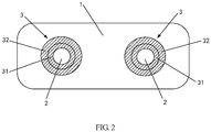
- FIG. 2 is a structural schematic diagram of a positioning structure according to a second embodiment of the present invention.
- the positioning structure according to the second embodiment of the present invention is substantially the same as the positioning structure according to the first embodiment of the present invention.
- a reinforcing layer 3 in the positioning structure according to the second embodiment of the present invention includes a hard layer 31 and a protective film 32, and the hard layer 31 and the protective film 32 are laid on a same surface of a flexible substrate 1.
- An inner periphery of the hard layer 31 coincides with a periphery of a positioning hole 2.
- the protective film 32 is attached to a side of the hard layer 31 that is away from the positioning hole 2, and the hard layer 31 is partially or entirely covered by the protective film 32.
- the hard layer 31 is an annulate strip, and an inner periphery of the hard layer 31 coincides with the periphery of the positioning hole 2.
- the hard layer 31 is a metal plating layer made of a copper foil.
- the hard layer 31 is a metal plating layer made of an aluminum foil.
- the hard layer 31 is a sprayed hard coating layer.
- the hard layer 31 is a strengthening layer.
- a material of the strengthening layer includes, but is not limited to, a cover film or a cover layer, etc., which have both insulation protection and reinforcing effects.
- each strengthening layer may include one or more sublayers, and the number of the sublayers and the materials of the sublayers may be set freely according to an actual condition.
- the protective film 32 also has functions of avoiding oxidation of the hard layer 31, covering for a subsequent surface treatment, and acting as a solder resist in subsequent Surface Mount Technology (SMT).
- SMT Surface Mount Technology
- the positioning holes 2 are formed in the flexible substrate 1, and the hard layers 31 are laid on peripheries of the positioning holes 2 of at least one surface of the flexible substrate 1.
- the protective films 32 are laid on sides of the hard layers 31 which are away from the flexible substrate 1. An inner periphery of the protective film 32 and the inner periphery of the hard layer 31 are coincided, and an outer periphery of the protective film 32 is larger than an outer periphery of the hard layer 31.
- the positioning holes 2 are formed on the flexible substrate 1, the reinforcing layers 3 are laid along the peripheries of the positioning holes 2, the reinforcing layer 3 includes the hard layer 31 and the protective film 32, and the hard layer 31 and the protective film 32 are laid on the same surface of the flexible substrate 1, the inner periphery of the hard layer 31 and the periphery of the positioning hole 2 are coincided, the protective film 32 is attached to the side of the hard layer 31 that is away from the positioning hole 2, and the hard layer 31 is partially or entirely covered by the protective film 32. Therefore, the strength of the positioning holes 2 is improved, an undesirable deformation of the positioning holes 2 under external forces is prevented, and positioning accuracy decrease of the positioning holes 2 caused by the undesirable deformation of the positioning holes 2 is avoided.
- the reinforcing layer 3 contains the hard layer 31 and excludes the protective film 32.
- the hard layer 31 is disposed on the flexible substrate 1 and is located within a preset range around the periphery of the positioning hole 2.
- the hard layer 31 has a hole aligned with the positioning hole 2.
- the strength of the positioning hole 2 is improved by means of the hard layer 31, so as to avoid the undesirable deformation of the positioning hole 2 under the external forces.
- FIG. 3 is a structural schematic diagram of a positioning structure according to a third embodiment of the present invention.
- the positioning structure according to the third embodiment of the present invention is substantially the same as the positioning structure according to the first embodiment of the present invention.
- a reinforcing layer 3 in the positioning structure according to the third embodiment of the present invention includes a hard layer 31 and a protective film 32, and the hard layer 31 and the protective film 32 are laid on a same surface of a flexible substrate 1.
- An inner periphery of the hard layer 31 coincides with a periphery of a positioning hole 2, and an inner periphery of the protective film 32 coincides with an outer periphery of the hard layer 31.
- the hard layer 31 is an annulate strip, and the inner periphery of the hard layer 31 coincides with the periphery of the positioning hole 2.
- the hard layer 31 is a metal plating layer made of a copper foil.
- the hard layer 31 is a metal plating layer made of an aluminum foil.
- the hard layer 31 is a sprayed hard coating layer.
- the positioning holes 2 are formed in the flexible substrate 1, and the hard layers 31 are laid on the peripheries of the positioning holes 2 of at least one surface of the flexible substrate 1.
- the protective films 32 are laid on sides of the hard layers 31 which are away from the flexible substrate 1, the inner periphery of the protective film 32 and an outer periphery of the hard layer 31 are coincided.
- the positioning holes 2 are formed on the flexible substrate 1, the reinforcing layers 3 are laid along the peripheries of the positioning holes 2, the reinforcing layer 3 includes the hard layer 31 and the protective film 32, and the hard layer 31 and the protective film 32 are laid on the same surface of the flexible substrate 1, the inner periphery of the hard layer 31 and the periphery of the positioning hole 2 are coincided, the protective film 32 is attached to the side of the hard layer 31 that is away from the positioning hole 2, the inner periphery of the protective film 32 and the outer periphery of the hard layer 31 are coincided. Therefore, the strength of the positioning holes 2 is improved, an undesirable deformation of the positioning holes 2 under external forces is prevented, and positioning accuracy decrease of the positioning holes 2 caused by the undesirable deformation of the positioning holes 2 is avoided.
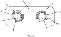
- FIG. 4 is a structural schematic diagram of a positioning structure according to a fourth embodiment of the present invention.
- the positioning structure according to the fourth embodiment of the present invention is substantially the same as the positioning structure according to the third embodiment of the present invention.
- a hard layer 31 in the positioning structure according to the fourth embodiment of the present invention includes two semicircular annulate strips, and the two semicircular annulate strips are evenly distributed along a periphery of a positioning hole 2, inner peripheries of the two semicircular annulate strips and the periphery of the positioning hole 2 are coincided.
- the positioning holes 2 are formed on a flexible substrate 1, reinforcing layers 3 are laid along the peripheries of the positioning holes 2, the reinforcing layer 3 includes the hard layer 31 and a protective film 32, the hard layer 31 and the protective film 32 are laid on a same surface of the flexible substrate 1, the hard layer 31 is set as the two semicircular annulate strips which are distributed evenly along the periphery of the positioning hole 2, the inner peripheries of the two semicircular annulate strips and the periphery of the positioning hole 2 are coincided, the protective film 32 is attached to a side of the hard layer 31 that is away from the positioning hole 2, an inner periphery of the protective film 32 and an outer periphery of the hard layer 31 are coincided. Therefore, the strength of the positioning holes 2 is improved, an undesirable deformation of the positioning holes 2 under external forces is prevented, and positioning accuracy decrease of the positioning holes 2 caused by the undesirable deformation of the positioning holes 2 is avoided.
- FIG. 5 is a structural schematic diagram of a positioning structure according to a fifth embodiment of the present invention.
- the positioning structure according to the fifth embodiment of the present invention is substantially the same as the positioning structure according to the third embodiment of the present invention.
- a hard layer 31 in the positioning structure according to the fifth embodiment of the present invention includes three fanning strips, and the three fanning strips are evenly and annularly distributed along a periphery of a positioning hole 2.
- a fan-shaped gap is included between two adjacent strips, inner peripheries of the three fanning strips and the periphery of the positioning hole 2 are coincided.
- the positioning holes 2 are formed on a flexible substrate 1, reinforcing layers 3 are laid along the peripheries of the positioning holes 2, a reinforcing layer 3 includes the hard layer 31 and a protective film 32, and the hard layer 31 and the protective film 32 are laid on a same surface of the flexible substrate 1, the hard layer 31 is set as the three fanning strips which are annular distributed evenly along the periphery of the positioning hole 2, the inner peripheries of the three fanning strips and the periphery of the positioning hole 2 are coincided, the protective film 32 is attached to a side of the hard layer 31 that is away from the positioning hole 2, an inner periphery of the protective film 32 and an outer periphery of the hard layer 31 are coincided. Therefore, the strength of the positioning holes 2 is improved, an undesirable deformation of the positioning holes 2 under external forces is prevented, and positioning accuracy decrease of the positioning holes 2 caused by the undesirable deformation of the positioning holes 2 is avoided.
- FIG. 6 is a structural schematic diagram of a positioning structure according to a sixth embodiment of the present invention.
- the positioning structure according to the sixth embodiment of the present invention is substantially the same as the positioning structure according to the third embodiment of the present invention.
- a hard layer 31 in the positioning structure according to the sixth embodiment of the present invention includes a plurality of circular strips, and the plurality of circular strips are evenly and annularly distributed along a periphery of a positioning hole 2.
- shapes of the hard layers 31 may be set freely according to an actual condition.
- the hard layer 31 may include a plurality of segments. Shapes of the segments in the hard layer 31 may be set freely according to the actual condition, and are not limited to the shape mentioned in the above embodiments of the present invention.
- the shapes of the segments in the hard layer 31 may be elliptical shapes or irregular shapes.
Landscapes
- Engineering & Computer Science (AREA)
- Microelectronics & Electronic Packaging (AREA)
- Manufacturing & Machinery (AREA)
- Structure Of Printed Boards (AREA)
- Non-Metallic Protective Coatings For Printed Circuits (AREA)
Abstract
Description
- The present invention relates to the field of bonding technology, and in particular to a positioning structure and a flexible printed circuit.
- A flexible printed circuit is a printed circuit board made of a flexible insulating substrate, and is capable of being bent, wound and folded freely. The flexible printed circuit is available in single-sided, multi-sided and multi-layer boards and other types, and it is mainly formed by laying a cover film with mechanical protection and good electrical insulation properties on a surface of the flexible insulating substrate and pressing the cover film to the surface of the flexible insulating substrate.
- However, in an existing FOF (i.e., FPC ON FPC, Flexible Printed Circuit bonding Flexible Printed Circuit) process, because a material around a positioning hole of the flexible printed circuit is soft and weak, the positioning hole is prone to deformation under action of a positioning device force and other external forces, and the deformed positioning hole may result in inaccurate positioning and even result in bonding failure of the flexible printed circuit during a positioning process.
- In view of this, embodiments of the present invention provide a positioning structure and a flexible printed circuit, in order to solve the problem that the positioning hole is easily deformed under action of external forces.
- In a first aspect, a positioning structure according to an embodiment of the present invention includes a flexible substrate having a positioning hole therein and a reinforcing layer disposed on the flexible substrate and located within a preset range around a periphery of the positioning hole to reinforce the positioning hole, and the reinforcing layer includes a hole corresponding to the positioning hole.
- In an embodiment of the present invention, the reinforcing layer includes a hard layer. The hard layer is disposed on the flexible substrate and is located within the preset range around the periphery of the positioning hole, and the hard layer has a hole aligned with the positioning hole.
- In an embodiment of the present invention, the reinforcement layer further includes a protective film disposed on the flexible substrate and located within the preset range around the periphery of the positioning hole, and the hard layer is partially or entirely covered by the protective film.
- In an embodiment of the present invention, the reinforcing layer further includes a protective film disposed on the flexible substrate and located within a preset range around the hard layer, and an inner periphery of the protective film coincides with an outer periphery of the hard layer.
- In an embodiment of the present invention, the hard layer includes a metal plating layer or a hard coating layer or a strengthening layer.
- In an embodiment of the present invention, the positioning hole is circular-shaped, the protective film is annular-shaped, and the hard layer is annular-shaped.
- In an embodiment of the present invention, the hard layer includes a plurality of segments, and the segments are annularly distributed along the periphery of the positioning hole.
- In an embodiment of the present invention, the positioning hole is circular-shaped, the protective film is annular-shaped, and each of the plurality of segments is one of a circular shape, a fan shape, a semicircular shape, and an irregular shape.
- In an embodiment of the present invention, a distance between an outer periphery of the reinforcing layer and a periphery of the positioning hole is in a range of 0 mm to 10 mm.
- In a second aspect, a flexible printed circuit according to an embodiment of the present invention includes an electronic device and the positioning structure according to the first aspect described.
- In the positioning structure according to the embodiments of the present invention, the strength of the positioning hole is improved and an undesirable deformation phenomenon of the positioning hole under action of external forces is prevented, by disposing the positioning hole on the flexible substrate and laying the reinforcing layer in the preset range around the periphery of the positioning hole.
-
-
FIG. 1 is a structural schematic diagram of a positioning structure according to a first embodiment of the present invention. -
FIG. 2 is a structural schematic diagram of a positioning structure according to a second embodiment of the present invention. -
FIG. 3 is a structural schematic diagram of a positioning structure according to a third embodiment of the present invention. -
FIG. 4 is a structural schematic diagram of a positioning structure according to a fourth embodiment of the present invention. -
FIG. 5 is a structural schematic diagram of a positioning structure according to a fifth embodiment of the present invention. -
FIG. 6 is a structural schematic diagram of a positioning structure according to a sixth embodiment of the present invention. - In order to make objects, technical means and advantages of the present invention more comprehensible, the present invention is to be further described in detail below with reference to accompanying drawings. The advantages and features of the present invention will be more apparent according to following description and claims. It may be noted that the accompanying drawings are all in a very simplified form and all use non-precise proportions, so as to conveniently and clearly state embodiments of the present invention.
-
FIG. 1 is a structural schematic diagram of a positioning structure according to a first embodiment of the present invention. As shown inFIG.1 , the positioning structure according to the first embodiment of the present invention includes aflexible substrate 1 having positioningholes 2 therein and reinforcinglayers 3. The reinforcinglayers 3 are disposed on theflexible substrate 1 and are located within preset ranges around peripheries of thepositioning holes 2 to reinforce thepositioning holes 2. The reinforcinglayers 3 have holes corresponding to thepositioning holes 2. - In the positioning structure according to the first embodiment of the present invention, the
positioning holes 2 are disposed on theflexible substrate 1 and the reinforcinglayers 3 are laid in the preset ranges around the peripheries of thepositioning holes 2. Therefore, the strength of thepositioning holes 2 is improved and an undesirable deformation phenomenon of thepositioning holes 2 under action of external forces is prevented. - It may be understood that the holes in the reinforcing
layers 3 may be the same size as thepositioning hole 2 or may be larger than thepositioning hole 2. - It may be understood that the preset ranges in which the reinforcing
layers 3 are disposed around the peripheries of thepositioning holes 2 may be freely set according to an actual condition. For example, the preset ranges may be set from 0 mm to 10 mm, that is, distances between outer peripheries of the reinforcinglayers 3 and the peripheries of thepositioning holes 2 are in a range of 0 mm to 10 mm, which will improve functions of the reinforcinglayers 3 without impacting structures around thepositioning holes 2. In addition, a size of the preset range may also be set according to the size of thepositioning hole 2. For example, the larger a radius of thepositioning hole 2, the larger the preset range is. - It may be understood that the sizes and shapes of the
positioning holes 2 formed on theflexible substrate 1 may be freely set according to the actual condition. For example, thepositioning holes 2 are set to be circular holes with the radius of 5 mm, and the embodiments of the present invention are not limited to this. Instead, the shapes of thepositioning holes 2 may also be square or oval. - It may be understood that the reinforcing
layers 3 may be disposed on an upper and/or a lower surface of theflexible substrate 1 on which thepositioning holes 2 are formed, so as to substantially enhance the expansibility and the adaptability of the positioning structure according to the embodiments of the present invention. - In an embodiment of the present invention, the
reinforcing layer 3 is an annulate strip, an inner periphery of the reinforcinglayer 3 coincides with the periphery of thepositioning hole 2. With arranging the reinforcinglayer 3 as the annulate strip, thepositioning hole 2 is fixed sufficiently by the reinforcinglayer 3 and material cost and resources are saved at the same time. It may be understood that a shape of the reinforcinglayer 3 may also be set according to the shape of thepositioning hole 2. For example, when the shape of thepositioning hole 2 is square, the reinforcinglayer 3 may be a square ring, and when the shape of thepositioning hole 2 is elliptical, the reinforcinglayer 3 may be an elliptical ring. Certainly, the shape of the reinforcinglayer 3 may also be different from the shape of thepositioning hole 2. For example, when the shape of thepositioning hole 2 is circular-shaped, the reinforcinglayer 3 may be a square ring. - It may be understood that the shape of the reinforcing
layer 3 may be set freely according to the actual condition. For example, the reinforcinglayer 3 may include a plurality of segments, and the plurality of segments are annularly distributed along the periphery of thepositioning hole 2 so as to reinforce thepositioning hole 2. In addition, shapes of the segments may be freely set according to the actual condition, and the shapes of the segments include one or a combination of following shapes: a diamond shape, a circle shape, a fan shape and so on. - In an embodiment of the present invention, the
flexible substrate 1 is a flexible printed circuit. In an actual application process, when a Driver Flexible Printed Circuit (Driver FPC) and a Touch Panel Flexible Printed Circuit (TP FPC) are required to be bonded to achieve electrical conduction, positioningholes 2 of the Driver FPC and/or positioningholes 2 of the TP FPC are subjected to a treatment of laying the reinforcinglayers 3 on an upper and/or a lower surface, so as to sufficiently increase the strength and the hardness of thepositioning holes 2, and make thepositioning holes 2 on the flexible printed circuit sufficiently adapt to different actual conditions and usage requirements. Therefore, the adaptability and the expansibility of the positioning structure according to the embodiments of the present invention are increased. - In an embodiment of the present invention, materials of the reinforcing
layers 3 include, but are not limited to, a polyimide film, a cover film, a cover layer and other materials, which have both insulation protection and reinforcing effects. In addition, it may be understood that each reinforcinglayer 3 may include one or more sublayers, and the number of the sublayers and materials of the sublayers may be set freely according to the actual condition. - According to the first embodiment of the present invention, in the actual application process, the
positioning holes 2 are formed in theflexible substrate 1, and the reinforcinglayers 3 are disposed on the peripheries of thepositioning holes 2 of at least one surface of theflexible substrate 1. Therefore, the strength and the hardness of the peripheries of thepositioning holes 2 are strengthened, so as to prevent thepositioning holes 2 from being deformed by the external forces. -
FIG. 2 is a structural schematic diagram of a positioning structure according to a second embodiment of the present invention. As shown inFIG. 2 , the positioning structure according to the second embodiment of the present invention is substantially the same as the positioning structure according to the first embodiment of the present invention. The following only highlights differences, and similarities are not repeated here. A reinforcinglayer 3 in the positioning structure according to the second embodiment of the present invention includes ahard layer 31 and aprotective film 32, and thehard layer 31 and theprotective film 32 are laid on a same surface of aflexible substrate 1. An inner periphery of thehard layer 31 coincides with a periphery of apositioning hole 2. Theprotective film 32 is attached to a side of thehard layer 31 that is away from thepositioning hole 2, and thehard layer 31 is partially or entirely covered by theprotective film 32. - In an embodiment of the present invention, the
hard layer 31 is an annulate strip, and an inner periphery of thehard layer 31 coincides with the periphery of thepositioning hole 2. - In an embodiment of the present invention, the
hard layer 31 is a metal plating layer made of a copper foil. - In an embodiment of the present invention, the
hard layer 31 is a metal plating layer made of an aluminum foil. - In an embodiment of the present invention, the
hard layer 31 is a sprayed hard coating layer. - In an embodiment of the present invention, the
hard layer 31 is a strengthening layer. - In an embodiment of the present invention, a material of the strengthening layer includes, but is not limited to, a cover film or a cover layer, etc., which have both insulation protection and reinforcing effects. In addition, it may be understood that each strengthening layer may include one or more sublayers, and the number of the sublayers and the materials of the sublayers may be set freely according to an actual condition.
- In an embodiment of the present invention, the
protective film 32 also has functions of avoiding oxidation of thehard layer 31, covering for a subsequent surface treatment, and acting as a solder resist in subsequent Surface Mount Technology (SMT). - In an actual application process, the positioning holes 2 are formed in the
flexible substrate 1, and thehard layers 31 are laid on peripheries of the positioning holes 2 of at least one surface of theflexible substrate 1. Theprotective films 32 are laid on sides of thehard layers 31 which are away from theflexible substrate 1. An inner periphery of theprotective film 32 and the inner periphery of thehard layer 31 are coincided, and an outer periphery of theprotective film 32 is larger than an outer periphery of thehard layer 31. - In the positioning structure according to the second embodiment of the present invention, the positioning holes 2 are formed on the
flexible substrate 1, the reinforcinglayers 3 are laid along the peripheries of the positioning holes 2, the reinforcinglayer 3 includes thehard layer 31 and theprotective film 32, and thehard layer 31 and theprotective film 32 are laid on the same surface of theflexible substrate 1, the inner periphery of thehard layer 31 and the periphery of thepositioning hole 2 are coincided, theprotective film 32 is attached to the side of thehard layer 31 that is away from thepositioning hole 2, and thehard layer 31 is partially or entirely covered by theprotective film 32. Therefore, the strength of the positioning holes 2 is improved, an undesirable deformation of the positioning holes 2 under external forces is prevented, and positioning accuracy decrease of the positioning holes 2 caused by the undesirable deformation of the positioning holes 2 is avoided. - In an embodiment of the present invention, the reinforcing
layer 3 contains thehard layer 31 and excludes theprotective film 32. Thehard layer 31 is disposed on theflexible substrate 1 and is located within a preset range around the periphery of thepositioning hole 2. Thehard layer 31 has a hole aligned with thepositioning hole 2. In the positioning structure according to the embodiments of the present invention, the strength of thepositioning hole 2 is improved by means of thehard layer 31, so as to avoid the undesirable deformation of thepositioning hole 2 under the external forces. -
FIG. 3 is a structural schematic diagram of a positioning structure according to a third embodiment of the present invention. As shown inFIG. 3 , the positioning structure according to the third embodiment of the present invention is substantially the same as the positioning structure according to the first embodiment of the present invention. The following only highlights differences, and similarities are not repeated here. A reinforcinglayer 3 in the positioning structure according to the third embodiment of the present invention includes ahard layer 31 and aprotective film 32, and thehard layer 31 and theprotective film 32 are laid on a same surface of aflexible substrate 1. An inner periphery of thehard layer 31 coincides with a periphery of apositioning hole 2, and an inner periphery of theprotective film 32 coincides with an outer periphery of thehard layer 31. - In an embodiment of the present invention, the
hard layer 31 is an annulate strip, and the inner periphery of thehard layer 31 coincides with the periphery of thepositioning hole 2. - In an embodiment of the present invention, the
hard layer 31 is a metal plating layer made of a copper foil. - In an embodiment of the present invention, the
hard layer 31 is a metal plating layer made of an aluminum foil. - In an embodiment of the present invention, the
hard layer 31 is a sprayed hard coating layer. - In an actual application process, the positioning holes 2 are formed in the
flexible substrate 1, and thehard layers 31 are laid on the peripheries of the positioning holes 2 of at least one surface of theflexible substrate 1. Theprotective films 32 are laid on sides of thehard layers 31 which are away from theflexible substrate 1, the inner periphery of theprotective film 32 and an outer periphery of thehard layer 31 are coincided. - In the positioning structure according to the third embodiment of the present invention, the positioning holes 2 are formed on the
flexible substrate 1, the reinforcinglayers 3 are laid along the peripheries of the positioning holes 2, the reinforcinglayer 3 includes thehard layer 31 and theprotective film 32, and thehard layer 31 and theprotective film 32 are laid on the same surface of theflexible substrate 1, the inner periphery of thehard layer 31 and the periphery of thepositioning hole 2 are coincided, theprotective film 32 is attached to the side of thehard layer 31 that is away from thepositioning hole 2, the inner periphery of theprotective film 32 and the outer periphery of thehard layer 31 are coincided. Therefore, the strength of the positioning holes 2 is improved, an undesirable deformation of the positioning holes 2 under external forces is prevented, and positioning accuracy decrease of the positioning holes 2 caused by the undesirable deformation of the positioning holes 2 is avoided. -
FIG. 4 is a structural schematic diagram of a positioning structure according to a fourth embodiment of the present invention. As shown inFIG. 4 , the positioning structure according to the fourth embodiment of the present invention is substantially the same as the positioning structure according to the third embodiment of the present invention. The following only highlights differences, and similarities are not repeated here. Ahard layer 31 in the positioning structure according to the fourth embodiment of the present invention includes two semicircular annulate strips, and the two semicircular annulate strips are evenly distributed along a periphery of apositioning hole 2, inner peripheries of the two semicircular annulate strips and the periphery of thepositioning hole 2 are coincided. - In the positioning structure according to the fourth embodiment of the present invention, the positioning holes 2 are formed on a
flexible substrate 1, reinforcinglayers 3 are laid along the peripheries of the positioning holes 2, the reinforcinglayer 3 includes thehard layer 31 and aprotective film 32, thehard layer 31 and theprotective film 32 are laid on a same surface of theflexible substrate 1, thehard layer 31 is set as the two semicircular annulate strips which are distributed evenly along the periphery of thepositioning hole 2, the inner peripheries of the two semicircular annulate strips and the periphery of thepositioning hole 2 are coincided, theprotective film 32 is attached to a side of thehard layer 31 that is away from thepositioning hole 2, an inner periphery of theprotective film 32 and an outer periphery of thehard layer 31 are coincided. Therefore, the strength of the positioning holes 2 is improved, an undesirable deformation of the positioning holes 2 under external forces is prevented, and positioning accuracy decrease of the positioning holes 2 caused by the undesirable deformation of the positioning holes 2 is avoided. -
FIG. 5 is a structural schematic diagram of a positioning structure according to a fifth embodiment of the present invention. As shown inFIG. 5 , the positioning structure according to the fifth embodiment of the present invention is substantially the same as the positioning structure according to the third embodiment of the present invention. The following only highlights differences, and similarities are not repeated here. Ahard layer 31 in the positioning structure according to the fifth embodiment of the present invention includes three fanning strips, and the three fanning strips are evenly and annularly distributed along a periphery of apositioning hole 2. A fan-shaped gap is included between two adjacent strips, inner peripheries of the three fanning strips and the periphery of thepositioning hole 2 are coincided. - In the positioning structure according to the fifth embodiment of the present invention, the positioning holes 2 are formed on a
flexible substrate 1, reinforcinglayers 3 are laid along the peripheries of the positioning holes 2, a reinforcinglayer 3 includes thehard layer 31 and aprotective film 32, and thehard layer 31 and theprotective film 32 are laid on a same surface of theflexible substrate 1, thehard layer 31 is set as the three fanning strips which are annular distributed evenly along the periphery of thepositioning hole 2, the inner peripheries of the three fanning strips and the periphery of thepositioning hole 2 are coincided, theprotective film 32 is attached to a side of thehard layer 31 that is away from thepositioning hole 2, an inner periphery of theprotective film 32 and an outer periphery of thehard layer 31 are coincided. Therefore, the strength of the positioning holes 2 is improved, an undesirable deformation of the positioning holes 2 under external forces is prevented, and positioning accuracy decrease of the positioning holes 2 caused by the undesirable deformation of the positioning holes 2 is avoided. -
FIG. 6 is a structural schematic diagram of a positioning structure according to a sixth embodiment of the present invention. As shown inFIG. 6 , the positioning structure according to the sixth embodiment of the present invention is substantially the same as the positioning structure according to the third embodiment of the present invention. The following only highlights differences, and similarities are not repeated here. Ahard layer 31 in the positioning structure according to the sixth embodiment of the present invention includes a plurality of circular strips, and the plurality of circular strips are evenly and annularly distributed along a periphery of apositioning hole 2. - In the positioning structure according to the sixth embodiment of the present invention, the positioning holes 2 are formed on a
flexible substrate 1, reinforcinglayers 3 are laid along the peripheries of the positioning holes 2, the reinforcinglayer 3 includes thehard layer 31 and aprotective film 32, thehard layer 31 and theprotective film 32 are laid on a same surface of theflexible substrate 1, thehard layer 31 is set as the plurality of circular strips which are annular distributed evenly along the periphery of thepositioning hole 2, theprotective film 32 is attached to a side of thehard layer 31 that is away from thepositioning hole 2, an inner periphery of theprotective film 32 and an outer periphery of thehard layer 31 are coincided. Therefore, the strength of the positioning holes 2 is improved, an undesirable deformation of the positioning holes 2 under external forces is prevented, and positioning accuracy decrease of the positioning holes 2 caused by the undesirable deformation of the positioning holes 2 is avoided. - It may be understood that shapes of the
hard layers 31 may be set freely according to an actual condition. For example, thehard layer 31 may include a plurality of segments. Shapes of the segments in thehard layer 31 may be set freely according to the actual condition, and are not limited to the shape mentioned in the above embodiments of the present invention. For example, the shapes of the segments in thehard layer 31 may be elliptical shapes or irregular shapes. - The foregoing descriptions are merely preferred embodiments of the present invention, but the protection scope of the present invention is not limited hereto. Any modifications, equivalent replacements or improvements, etc. made within the spirit and principles of the present invention are intended to be included in the scope of protection of the present invention.
Claims (10)
- A positioning structure, characterized in that the positioning structure comprises:a flexible substrate having a positioning hole; anda reinforcing layer disposed on the flexible substrate and located within a preset range around a periphery of the positioning hole to reinforce the positioning hole, the reinforcing layer including a hole corresponding to the positioning hole.
- The positioning structure of claim 1, wherein the reinforcing layer comprises a hard layer disposed on the flexible substrate and located within the preset range around the periphery of the positioning hole, and the hard layer includes a hole aligned with the positioning hole.
- The positioning structure of claim 2, wherein the reinforcing layer further comprises a protective film disposed on the flexible substrate and located within the preset range around the periphery of the positioning hole, and the hard layer is partially or entirely covered by the protective film.
- The positioning structure of claim 2, wherein the reinforcing layer further comprises a protective film disposed on the flexible substrate and located within a preset range around the hard layer, and an inner periphery of the protective film coincides with an outer periphery of the hard layer.
- The positioning structure of any one of claims 2 to 4, wherein the hard layer comprises a metal plating layer or a hard coating layer or a strengthening layer.
- The positioning structure of claim 3 or 4, wherein the positioning hole is circular-shaped, the protective film is annular-shaped, and the hard layer is annular-shaped.
- The positioning structure of claim 3 or 4, wherein the hard layer comprises a plurality of segments, and the plurality of segments are annularly distributed along the periphery of the positioning hole.
- The positioning structure of claim 7, wherein the positioning hole is circular-shaped, the protective film is annular-shaped, and each of the plurality of segments is one of a circular shape, a fan shape, a semicircular shape, and an irregular shape.
- The positioning structure of claim 1, wherein a distance between an outer periphery of the reinforcing layer and a periphery of the positioning hole is in a range of 0 mm to 10 mm.
- A flexible printed circuit, characterized in that the flexible printed circuit comprises:an electronic device; andthe positioning structure according to any one of claims 1 to 9.
Applications Claiming Priority (2)
| Application Number | Priority Date | Filing Date | Title |
|---|---|---|---|
| CN201721062229.3U CN207305037U (en) | 2017-08-23 | 2017-08-23 | Position pore structure and flexible PCB |
| PCT/CN2018/084881 WO2019037460A1 (en) | 2017-08-23 | 2018-04-27 | Positioning structure and flexible circuit board |
Publications (3)
| Publication Number | Publication Date |
|---|---|
| EP3598855A1 true EP3598855A1 (en) | 2020-01-22 |
| EP3598855A4 EP3598855A4 (en) | 2020-05-13 |
| EP3598855B1 EP3598855B1 (en) | 2024-04-17 |
Family
ID=62438654
Family Applications (1)
| Application Number | Title | Priority Date | Filing Date |
|---|---|---|---|
| EP18847835.8A Active EP3598855B1 (en) | 2017-08-23 | 2018-04-27 | Positioning structure and flexible circuit board |
Country Status (7)
| Country | Link |
|---|---|
| US (1) | US20190215954A1 (en) |
| EP (1) | EP3598855B1 (en) |
| JP (1) | JP6871414B2 (en) |
| KR (1) | KR102279493B1 (en) |
| CN (1) | CN207305037U (en) |
| TW (1) | TWM568573U (en) |
| WO (1) | WO2019037460A1 (en) |
Families Citing this family (2)
| Publication number | Priority date | Publication date | Assignee | Title |
|---|---|---|---|---|
| CN108684145A (en) * | 2018-05-07 | 2018-10-19 | 潘玥铭 | A method of improving PCB Aligning degrees |
| CN113056095A (en) * | 2021-02-22 | 2021-06-29 | 深圳市亚微科技有限公司 | FPC suitable for pin insertion |
Family Cites Families (15)
| Publication number | Priority date | Publication date | Assignee | Title |
|---|---|---|---|---|
| JPH0760917B2 (en) * | 1988-08-19 | 1995-06-28 | 富士写真光機株式会社 | Flexible printed circuit board |
| JPH06310819A (en) * | 1993-04-26 | 1994-11-04 | Hitachi Telecom Technol Ltd | Printed wiring board structure |
| JP3493714B2 (en) * | 1994-02-14 | 2004-02-03 | 株式会社ニコン | Printed board |
| DE19653360A1 (en) * | 1996-12-20 | 1998-06-25 | Bosch Gmbh Robert | Conductive foil for the conductive connection of electrical and / or electronic components |
| JP4117892B2 (en) * | 2004-09-29 | 2008-07-16 | 三井金属鉱業株式会社 | Film carrier tape for mounting electronic components and flexible substrate |
| CN100574555C (en) * | 2007-07-04 | 2009-12-23 | 富葵精密组件(深圳)有限公司 | Flexible substrate of circuit board |
| JP5510795B2 (en) * | 2008-01-30 | 2014-06-04 | 日本電気株式会社 | Electronic component mounting structure, electronic component mounting method, and electronic component mounting substrate |
| JP2010135622A (en) * | 2008-12-05 | 2010-06-17 | Tokai Rika Co Ltd | Circuit board and electronic apparatus provided with circuit board |
| US8535623B2 (en) * | 2009-04-21 | 2013-09-17 | Hitachi Chemical Company, Ltd. | Concave connector substrate, method of manufacturing the same, measuring kit, sensor substrate, and sensor substrate interprolated cylinder |
| JP2011049316A (en) * | 2009-08-26 | 2011-03-10 | Nitto Denko Corp | Printed circuit board and method of manufacturing the same |
| CN201616955U (en) * | 2010-03-12 | 2010-10-27 | 上海天马微电子有限公司 | Flexible printed circuit board |
| CN203194007U (en) * | 2013-02-03 | 2013-09-11 | 周伟庆 | Circuit board |
| CN203279331U (en) * | 2013-04-19 | 2013-11-06 | 统赢软性电路(珠海)有限公司 | Novel positioning hole structure for circuit board |
| US9831205B2 (en) * | 2013-11-18 | 2017-11-28 | Taiwan Semiconductor Manufacturing Company Ltd. | Semiconductor device and manufacturing method thereof |
| CN205283935U (en) * | 2015-12-29 | 2016-06-01 | 常州海弘电子有限公司 | PCB board with position circle protective layer |
-
2017
- 2017-08-23 CN CN201721062229.3U patent/CN207305037U/en active Active
-
2018
- 2018-04-27 KR KR1020197029042A patent/KR102279493B1/en active Active
- 2018-04-27 JP JP2019554400A patent/JP6871414B2/en active Active
- 2018-04-27 EP EP18847835.8A patent/EP3598855B1/en active Active
- 2018-04-27 WO PCT/CN2018/084881 patent/WO2019037460A1/en not_active Ceased
- 2018-06-08 TW TW107207686U patent/TWM568573U/en unknown
-
2019
- 2019-03-15 US US16/355,476 patent/US20190215954A1/en not_active Abandoned
Also Published As
| Publication number | Publication date |
|---|---|
| JP6871414B2 (en) | 2021-05-12 |
| EP3598855A4 (en) | 2020-05-13 |
| US20190215954A1 (en) | 2019-07-11 |
| TWM568573U (en) | 2018-10-11 |
| EP3598855B1 (en) | 2024-04-17 |
| WO2019037460A1 (en) | 2019-02-28 |
| CN207305037U (en) | 2018-05-01 |
| KR102279493B1 (en) | 2021-07-21 |
| KR20190119649A (en) | 2019-10-22 |
| JP2020513156A (en) | 2020-04-30 |
Similar Documents
| Publication | Publication Date | Title |
|---|---|---|
| JP2014112576A (en) | Shield film | |
| JP6053190B2 (en) | Printed wiring board | |
| KR101569156B1 (en) | Printed wiring board | |
| US11277919B2 (en) | Resin substrate and method for producing resin substrate | |
| JP2005317946A (en) | Circuit board | |
| US20190215954A1 (en) | Positioning structure and flexible printed circuit | |
| TWI446848B (en) | Method for manufacturing bending type printed circuit board | |
| JP2016040852A (en) | Shield film, shield printed wiring board, and method for manufacturing shield printed wiring board | |
| US20210385939A1 (en) | High-frequency circuit board and method for manufacturing the same | |
| CN105430889A (en) | Flexible circuit board and terminal | |
| US8071885B2 (en) | Printed circuit board | |
| KR101122721B1 (en) | Electric conductive gasket and method for manufacturing the same | |
| JP6139284B2 (en) | Shield film and printed wiring board | |
| JP6439197B2 (en) | Flexible printed wiring board and manufacturing method thereof | |
| JP6492758B2 (en) | Multi-wire wiring board | |
| JP2006269495A (en) | Flexible printed circuit board and semiconductor device | |
| US20160118346A1 (en) | Device embedded substrate and manufacturing method thereof | |
| JP2015012098A (en) | Shield film and printed wiring board | |
| JP2004079731A (en) | Flexible circuit board | |
| JP2006319197A (en) | Flex rigid board | |
| CN203788548U (en) | flexible circuit board | |
| CN102892251A (en) | Flexible Circuit Module | |
| JP2009231658A (en) | Circuit board | |
| JP2012195619A (en) | Flex-rigid printed wiring board | |
| CN107770944A (en) | Circuit board and its manufacture method with electro-magnetic screen function |
Legal Events
| Date | Code | Title | Description |
|---|---|---|---|
| STAA | Information on the status of an ep patent application or granted ep patent |
Free format text: STATUS: THE INTERNATIONAL PUBLICATION HAS BEEN MADE |
|
| PUAI | Public reference made under article 153(3) epc to a published international application that has entered the european phase |
Free format text: ORIGINAL CODE: 0009012 |
|
| STAA | Information on the status of an ep patent application or granted ep patent |
Free format text: STATUS: REQUEST FOR EXAMINATION WAS MADE |
|
| 17P | Request for examination filed |
Effective date: 20191014 |
|
| AK | Designated contracting states |
Kind code of ref document: A1 Designated state(s): AL AT BE BG CH CY CZ DE DK EE ES FI FR GB GR HR HU IE IS IT LI LT LU LV MC MK MT NL NO PL PT RO RS SE SI SK SM TR |
|
| AX | Request for extension of the european patent |
Extension state: BA ME |
|
| A4 | Supplementary search report drawn up and despatched |
Effective date: 20200417 |
|
| RIC1 | Information provided on ipc code assigned before grant |
Ipc: H05K 1/02 20060101AFI20200408BHEP Ipc: H05K 3/00 20060101ALN20200408BHEP |
|
| DAV | Request for validation of the european patent (deleted) | ||
| DAX | Request for extension of the european patent (deleted) | ||
| STAA | Information on the status of an ep patent application or granted ep patent |
Free format text: STATUS: EXAMINATION IS IN PROGRESS |
|
| 17Q | First examination report despatched |
Effective date: 20211011 |
|
| 17Q | First examination report despatched |
Effective date: 20211022 |
|
| GRAP | Despatch of communication of intention to grant a patent |
Free format text: ORIGINAL CODE: EPIDOSNIGR1 |
|
| STAA | Information on the status of an ep patent application or granted ep patent |
Free format text: STATUS: GRANT OF PATENT IS INTENDED |
|
| RIC1 | Information provided on ipc code assigned before grant |
Ipc: H05K 3/00 20060101ALN20240110BHEP Ipc: H05K 1/02 20060101AFI20240110BHEP |
|
| GRAS | Grant fee paid |
Free format text: ORIGINAL CODE: EPIDOSNIGR3 |
|
| INTG | Intention to grant announced |
Effective date: 20240208 |
|
| RIC1 | Information provided on ipc code assigned before grant |
Ipc: H05K 3/00 20060101ALN20240129BHEP Ipc: H05K 1/02 20060101AFI20240129BHEP |
|
| GRAA | (expected) grant |
Free format text: ORIGINAL CODE: 0009210 |
|
| STAA | Information on the status of an ep patent application or granted ep patent |
Free format text: STATUS: THE PATENT HAS BEEN GRANTED |
|
| AK | Designated contracting states |
Kind code of ref document: B1 Designated state(s): AL AT BE BG CH CY CZ DE DK EE ES FI FR GB GR HR HU IE IS IT LI LT LU LV MC MK MT NL NO PL PT RO RS SE SI SK SM TR |
|
| REG | Reference to a national code |
Ref country code: GB Ref legal event code: FG4D |
|
| REG | Reference to a national code |
Ref country code: CH Ref legal event code: EP |
|
| REG | Reference to a national code |
Ref country code: IE Ref legal event code: FG4D Ref country code: DE Ref legal event code: R096 Ref document number: 602018068311 Country of ref document: DE |
|
| REG | Reference to a national code |
Ref country code: LT Ref legal event code: MG9D |
|
| REG | Reference to a national code |
Ref country code: NL Ref legal event code: MP Effective date: 20240417 |
|
| REG | Reference to a national code |
Ref country code: AT Ref legal event code: MK05 Ref document number: 1678482 Country of ref document: AT Kind code of ref document: T Effective date: 20240417 |
|
| PG25 | Lapsed in a contracting state [announced via postgrant information from national office to epo] |
Ref country code: NL Free format text: LAPSE BECAUSE OF FAILURE TO SUBMIT A TRANSLATION OF THE DESCRIPTION OR TO PAY THE FEE WITHIN THE PRESCRIBED TIME-LIMIT Effective date: 20240417 |
|
| PG25 | Lapsed in a contracting state [announced via postgrant information from national office to epo] |
Ref country code: NL Free format text: LAPSE BECAUSE OF FAILURE TO SUBMIT A TRANSLATION OF THE DESCRIPTION OR TO PAY THE FEE WITHIN THE PRESCRIBED TIME-LIMIT Effective date: 20240417 |
|
| PG25 | Lapsed in a contracting state [announced via postgrant information from national office to epo] |
Ref country code: IS Free format text: LAPSE BECAUSE OF FAILURE TO SUBMIT A TRANSLATION OF THE DESCRIPTION OR TO PAY THE FEE WITHIN THE PRESCRIBED TIME-LIMIT Effective date: 20240817 |
|
| PG25 | Lapsed in a contracting state [announced via postgrant information from national office to epo] |
Ref country code: BG Free format text: LAPSE BECAUSE OF FAILURE TO SUBMIT A TRANSLATION OF THE DESCRIPTION OR TO PAY THE FEE WITHIN THE PRESCRIBED TIME-LIMIT Effective date: 20240417 |
|
| PG25 | Lapsed in a contracting state [announced via postgrant information from national office to epo] |
Ref country code: HR Free format text: LAPSE BECAUSE OF FAILURE TO SUBMIT A TRANSLATION OF THE DESCRIPTION OR TO PAY THE FEE WITHIN THE PRESCRIBED TIME-LIMIT Effective date: 20240417 Ref country code: FI Free format text: LAPSE BECAUSE OF FAILURE TO SUBMIT A TRANSLATION OF THE DESCRIPTION OR TO PAY THE FEE WITHIN THE PRESCRIBED TIME-LIMIT Effective date: 20240417 |
|
| PG25 | Lapsed in a contracting state [announced via postgrant information from national office to epo] |
Ref country code: GR Free format text: LAPSE BECAUSE OF FAILURE TO SUBMIT A TRANSLATION OF THE DESCRIPTION OR TO PAY THE FEE WITHIN THE PRESCRIBED TIME-LIMIT Effective date: 20240718 |
|
| PG25 | Lapsed in a contracting state [announced via postgrant information from national office to epo] |
Ref country code: PT Free format text: LAPSE BECAUSE OF FAILURE TO SUBMIT A TRANSLATION OF THE DESCRIPTION OR TO PAY THE FEE WITHIN THE PRESCRIBED TIME-LIMIT Effective date: 20240819 |
|
| PG25 | Lapsed in a contracting state [announced via postgrant information from national office to epo] |
Ref country code: ES Free format text: LAPSE BECAUSE OF FAILURE TO SUBMIT A TRANSLATION OF THE DESCRIPTION OR TO PAY THE FEE WITHIN THE PRESCRIBED TIME-LIMIT Effective date: 20240417 |
|
| PG25 | Lapsed in a contracting state [announced via postgrant information from national office to epo] |
Ref country code: AT Free format text: LAPSE BECAUSE OF FAILURE TO SUBMIT A TRANSLATION OF THE DESCRIPTION OR TO PAY THE FEE WITHIN THE PRESCRIBED TIME-LIMIT Effective date: 20240417 |
|
| PG25 | Lapsed in a contracting state [announced via postgrant information from national office to epo] |
Ref country code: PL Free format text: LAPSE BECAUSE OF FAILURE TO SUBMIT A TRANSLATION OF THE DESCRIPTION OR TO PAY THE FEE WITHIN THE PRESCRIBED TIME-LIMIT Effective date: 20240417 |
|
| PG25 | Lapsed in a contracting state [announced via postgrant information from national office to epo] |
Ref country code: LV Free format text: LAPSE BECAUSE OF FAILURE TO SUBMIT A TRANSLATION OF THE DESCRIPTION OR TO PAY THE FEE WITHIN THE PRESCRIBED TIME-LIMIT Effective date: 20240417 |
|
| PG25 | Lapsed in a contracting state [announced via postgrant information from national office to epo] |
Ref country code: PT Free format text: LAPSE BECAUSE OF FAILURE TO SUBMIT A TRANSLATION OF THE DESCRIPTION OR TO PAY THE FEE WITHIN THE PRESCRIBED TIME-LIMIT Effective date: 20240819 Ref country code: PL Free format text: LAPSE BECAUSE OF FAILURE TO SUBMIT A TRANSLATION OF THE DESCRIPTION OR TO PAY THE FEE WITHIN THE PRESCRIBED TIME-LIMIT Effective date: 20240417 Ref country code: NO Free format text: LAPSE BECAUSE OF FAILURE TO SUBMIT A TRANSLATION OF THE DESCRIPTION OR TO PAY THE FEE WITHIN THE PRESCRIBED TIME-LIMIT Effective date: 20240717 Ref country code: LV Free format text: LAPSE BECAUSE OF FAILURE TO SUBMIT A TRANSLATION OF THE DESCRIPTION OR TO PAY THE FEE WITHIN THE PRESCRIBED TIME-LIMIT Effective date: 20240417 Ref country code: IS Free format text: LAPSE BECAUSE OF FAILURE TO SUBMIT A TRANSLATION OF THE DESCRIPTION OR TO PAY THE FEE WITHIN THE PRESCRIBED TIME-LIMIT Effective date: 20240817 Ref country code: HR Free format text: LAPSE BECAUSE OF FAILURE TO SUBMIT A TRANSLATION OF THE DESCRIPTION OR TO PAY THE FEE WITHIN THE PRESCRIBED TIME-LIMIT Effective date: 20240417 Ref country code: GR Free format text: LAPSE BECAUSE OF FAILURE TO SUBMIT A TRANSLATION OF THE DESCRIPTION OR TO PAY THE FEE WITHIN THE PRESCRIBED TIME-LIMIT Effective date: 20240718 Ref country code: FI Free format text: LAPSE BECAUSE OF FAILURE TO SUBMIT A TRANSLATION OF THE DESCRIPTION OR TO PAY THE FEE WITHIN THE PRESCRIBED TIME-LIMIT Effective date: 20240417 Ref country code: ES Free format text: LAPSE BECAUSE OF FAILURE TO SUBMIT A TRANSLATION OF THE DESCRIPTION OR TO PAY THE FEE WITHIN THE PRESCRIBED TIME-LIMIT Effective date: 20240417 Ref country code: BG Free format text: LAPSE BECAUSE OF FAILURE TO SUBMIT A TRANSLATION OF THE DESCRIPTION OR TO PAY THE FEE WITHIN THE PRESCRIBED TIME-LIMIT Effective date: 20240417 Ref country code: AT Free format text: LAPSE BECAUSE OF FAILURE TO SUBMIT A TRANSLATION OF THE DESCRIPTION OR TO PAY THE FEE WITHIN THE PRESCRIBED TIME-LIMIT Effective date: 20240417 Ref country code: RS Free format text: LAPSE BECAUSE OF FAILURE TO SUBMIT A TRANSLATION OF THE DESCRIPTION OR TO PAY THE FEE WITHIN THE PRESCRIBED TIME-LIMIT Effective date: 20240717 |
|
| REG | Reference to a national code |
Ref country code: CH Ref legal event code: PL |
|
| PG25 | Lapsed in a contracting state [announced via postgrant information from national office to epo] |
Ref country code: LU Free format text: LAPSE BECAUSE OF NON-PAYMENT OF DUE FEES Effective date: 20240427 |
|
| REG | Reference to a national code |
Ref country code: BE Ref legal event code: MM Effective date: 20240430 |
|
| PG25 | Lapsed in a contracting state [announced via postgrant information from national office to epo] |
Ref country code: LU Free format text: LAPSE BECAUSE OF NON-PAYMENT OF DUE FEES Effective date: 20240427 |
|
| PG25 | Lapsed in a contracting state [announced via postgrant information from national office to epo] |
Ref country code: DK Free format text: LAPSE BECAUSE OF FAILURE TO SUBMIT A TRANSLATION OF THE DESCRIPTION OR TO PAY THE FEE WITHIN THE PRESCRIBED TIME-LIMIT Effective date: 20240417 |
|
| PG25 | Lapsed in a contracting state [announced via postgrant information from national office to epo] |
Ref country code: BE Free format text: LAPSE BECAUSE OF NON-PAYMENT OF DUE FEES Effective date: 20240430 |
|
| REG | Reference to a national code |
Ref country code: DE Ref legal event code: R097 Ref document number: 602018068311 Country of ref document: DE |
|
| PG25 | Lapsed in a contracting state [announced via postgrant information from national office to epo] |
Ref country code: EE Free format text: LAPSE BECAUSE OF FAILURE TO SUBMIT A TRANSLATION OF THE DESCRIPTION OR TO PAY THE FEE WITHIN THE PRESCRIBED TIME-LIMIT Effective date: 20240417 |
|
| PG25 | Lapsed in a contracting state [announced via postgrant information from national office to epo] |
Ref country code: CZ Free format text: LAPSE BECAUSE OF FAILURE TO SUBMIT A TRANSLATION OF THE DESCRIPTION OR TO PAY THE FEE WITHIN THE PRESCRIBED TIME-LIMIT Effective date: 20240417 |
|
| PG25 | Lapsed in a contracting state [announced via postgrant information from national office to epo] |
Ref country code: SK Free format text: LAPSE BECAUSE OF FAILURE TO SUBMIT A TRANSLATION OF THE DESCRIPTION OR TO PAY THE FEE WITHIN THE PRESCRIBED TIME-LIMIT Effective date: 20240417 Ref country code: RO Free format text: LAPSE BECAUSE OF FAILURE TO SUBMIT A TRANSLATION OF THE DESCRIPTION OR TO PAY THE FEE WITHIN THE PRESCRIBED TIME-LIMIT Effective date: 20240417 |
|
| PG25 | Lapsed in a contracting state [announced via postgrant information from national office to epo] |
Ref country code: SM Free format text: LAPSE BECAUSE OF FAILURE TO SUBMIT A TRANSLATION OF THE DESCRIPTION OR TO PAY THE FEE WITHIN THE PRESCRIBED TIME-LIMIT Effective date: 20240417 |
|
| PG25 | Lapsed in a contracting state [announced via postgrant information from national office to epo] |
Ref country code: SM Free format text: LAPSE BECAUSE OF FAILURE TO SUBMIT A TRANSLATION OF THE DESCRIPTION OR TO PAY THE FEE WITHIN THE PRESCRIBED TIME-LIMIT Effective date: 20240417 Ref country code: SK Free format text: LAPSE BECAUSE OF FAILURE TO SUBMIT A TRANSLATION OF THE DESCRIPTION OR TO PAY THE FEE WITHIN THE PRESCRIBED TIME-LIMIT Effective date: 20240417 Ref country code: RO Free format text: LAPSE BECAUSE OF FAILURE TO SUBMIT A TRANSLATION OF THE DESCRIPTION OR TO PAY THE FEE WITHIN THE PRESCRIBED TIME-LIMIT Effective date: 20240417 Ref country code: EE Free format text: LAPSE BECAUSE OF FAILURE TO SUBMIT A TRANSLATION OF THE DESCRIPTION OR TO PAY THE FEE WITHIN THE PRESCRIBED TIME-LIMIT Effective date: 20240417 Ref country code: DK Free format text: LAPSE BECAUSE OF FAILURE TO SUBMIT A TRANSLATION OF THE DESCRIPTION OR TO PAY THE FEE WITHIN THE PRESCRIBED TIME-LIMIT Effective date: 20240417 Ref country code: CZ Free format text: LAPSE BECAUSE OF FAILURE TO SUBMIT A TRANSLATION OF THE DESCRIPTION OR TO PAY THE FEE WITHIN THE PRESCRIBED TIME-LIMIT Effective date: 20240417 Ref country code: BE Free format text: LAPSE BECAUSE OF NON-PAYMENT OF DUE FEES Effective date: 20240430 Ref country code: MC Free format text: LAPSE BECAUSE OF FAILURE TO SUBMIT A TRANSLATION OF THE DESCRIPTION OR TO PAY THE FEE WITHIN THE PRESCRIBED TIME-LIMIT Effective date: 20240417 Ref country code: CH Free format text: LAPSE BECAUSE OF NON-PAYMENT OF DUE FEES Effective date: 20240430 |
|
| PG25 | Lapsed in a contracting state [announced via postgrant information from national office to epo] |
Ref country code: IT Free format text: LAPSE BECAUSE OF FAILURE TO SUBMIT A TRANSLATION OF THE DESCRIPTION OR TO PAY THE FEE WITHIN THE PRESCRIBED TIME-LIMIT Effective date: 20240417 |
|
| PLBE | No opposition filed within time limit |
Free format text: ORIGINAL CODE: 0009261 |
|
| STAA | Information on the status of an ep patent application or granted ep patent |
Free format text: STATUS: NO OPPOSITION FILED WITHIN TIME LIMIT |
|
| 26N | No opposition filed |
Effective date: 20250120 |
|
| PG25 | Lapsed in a contracting state [announced via postgrant information from national office to epo] |
Ref country code: IE Free format text: LAPSE BECAUSE OF NON-PAYMENT OF DUE FEES Effective date: 20240427 |
|
| PG25 | Lapsed in a contracting state [announced via postgrant information from national office to epo] |
Ref country code: SI Free format text: LAPSE BECAUSE OF FAILURE TO SUBMIT A TRANSLATION OF THE DESCRIPTION OR TO PAY THE FEE WITHIN THE PRESCRIBED TIME-LIMIT Effective date: 20240417 |
|
| PGFP | Annual fee paid to national office [announced via postgrant information from national office to epo] |
Ref country code: DE Payment date: 20250411 Year of fee payment: 8 |
|
| PGFP | Annual fee paid to national office [announced via postgrant information from national office to epo] |
Ref country code: GB Payment date: 20250417 Year of fee payment: 8 |
|
| PGFP | Annual fee paid to national office [announced via postgrant information from national office to epo] |
Ref country code: FR Payment date: 20250429 Year of fee payment: 8 |
|
| PG25 | Lapsed in a contracting state [announced via postgrant information from national office to epo] |
Ref country code: CY Free format text: LAPSE BECAUSE OF FAILURE TO SUBMIT A TRANSLATION OF THE DESCRIPTION OR TO PAY THE FEE WITHIN THE PRESCRIBED TIME-LIMIT; INVALID AB INITIO Effective date: 20180427 |
|
| PG25 | Lapsed in a contracting state [announced via postgrant information from national office to epo] |
Ref country code: HU Free format text: LAPSE BECAUSE OF FAILURE TO SUBMIT A TRANSLATION OF THE DESCRIPTION OR TO PAY THE FEE WITHIN THE PRESCRIBED TIME-LIMIT; INVALID AB INITIO Effective date: 20180427 |
|
| PG25 | Lapsed in a contracting state [announced via postgrant information from national office to epo] |
Ref country code: SE Free format text: LAPSE BECAUSE OF FAILURE TO SUBMIT A TRANSLATION OF THE DESCRIPTION OR TO PAY THE FEE WITHIN THE PRESCRIBED TIME-LIMIT Effective date: 20240417 |