EP3595003A1 - Power module substrate with heat sink - Google Patents
Power module substrate with heat sink Download PDFInfo
- Publication number
- EP3595003A1 EP3595003A1 EP18764394.5A EP18764394A EP3595003A1 EP 3595003 A1 EP3595003 A1 EP 3595003A1 EP 18764394 A EP18764394 A EP 18764394A EP 3595003 A1 EP3595003 A1 EP 3595003A1
- Authority
- EP
- European Patent Office
- Prior art keywords
- power
- thickness
- module substrate
- metal layer
- heat
- Prior art date
- Legal status (The legal status is an assumption and is not a legal conclusion. Google has not performed a legal analysis and makes no representation as to the accuracy of the status listed.)
- Granted
Links
Images



Classifications
-
- H—ELECTRICITY
- H05—ELECTRIC TECHNIQUES NOT OTHERWISE PROVIDED FOR
- H05K—PRINTED CIRCUITS; CASINGS OR CONSTRUCTIONAL DETAILS OF ELECTRIC APPARATUS; MANUFACTURE OF ASSEMBLAGES OF ELECTRICAL COMPONENTS
- H05K3/00—Apparatus or processes for manufacturing printed circuits
- H05K3/0058—Laminating printed circuit boards onto other substrates, e.g. metallic substrates
- H05K3/0061—Laminating printed circuit boards onto other substrates, e.g. metallic substrates onto a metallic substrate, e.g. a heat sink
-
- H—ELECTRICITY
- H10—SEMICONDUCTOR DEVICES; ELECTRIC SOLID-STATE DEVICES NOT OTHERWISE PROVIDED FOR
- H10W—GENERIC PACKAGES, INTERCONNECTIONS, CONNECTORS OR OTHER CONSTRUCTIONAL DETAILS OF DEVICES COVERED BY CLASS H10
- H10W70/00—Package substrates; Interposers; Redistribution layers [RDL]
- H10W70/60—Insulating or insulated package substrates; Interposers; Redistribution layers
- H10W70/67—Insulating or insulated package substrates; Interposers; Redistribution layers characterised by their insulating layers or insulating parts
- H10W70/68—Shapes or dispositions thereof
- H10W70/6875—Shapes or dispositions thereof being on a metallic substrate, e.g. insulated metal substrates [IMS]
-
- C—CHEMISTRY; METALLURGY
- C04—CEMENTS; CONCRETE; ARTIFICIAL STONE; CERAMICS; REFRACTORIES
- C04B—LIME, MAGNESIA; SLAG; CEMENTS; COMPOSITIONS THEREOF, e.g. MORTARS, CONCRETE OR LIKE BUILDING MATERIALS; ARTIFICIAL STONE; CERAMICS; REFRACTORIES; TREATMENT OF NATURAL STONE
- C04B35/00—Shaped ceramic products characterised by their composition; Ceramics compositions; Processing powders of inorganic compounds preparatory to the manufacturing of ceramic products
- C04B35/622—Forming processes; Processing powders of inorganic compounds preparatory to the manufacturing of ceramic products
- C04B35/64—Burning or sintering processes
- C04B35/645—Pressure sintering
-
- C—CHEMISTRY; METALLURGY
- C04—CEMENTS; CONCRETE; ARTIFICIAL STONE; CERAMICS; REFRACTORIES
- C04B—LIME, MAGNESIA; SLAG; CEMENTS; COMPOSITIONS THEREOF, e.g. MORTARS, CONCRETE OR LIKE BUILDING MATERIALS; ARTIFICIAL STONE; CERAMICS; REFRACTORIES; TREATMENT OF NATURAL STONE
- C04B37/00—Joining burned ceramic articles with other burned ceramic articles or other articles by heating
- C04B37/02—Joining burned ceramic articles with other burned ceramic articles or other articles by heating with metallic articles
- C04B37/023—Joining burned ceramic articles with other burned ceramic articles or other articles by heating with metallic articles characterised by the interlayer used
- C04B37/026—Joining burned ceramic articles with other burned ceramic articles or other articles by heating with metallic articles characterised by the interlayer used consisting of metals or metal salts
-
- H—ELECTRICITY
- H05—ELECTRIC TECHNIQUES NOT OTHERWISE PROVIDED FOR
- H05K—PRINTED CIRCUITS; CASINGS OR CONSTRUCTIONAL DETAILS OF ELECTRIC APPARATUS; MANUFACTURE OF ASSEMBLAGES OF ELECTRICAL COMPONENTS
- H05K1/00—Printed circuits
- H05K1/02—Details
-
- H—ELECTRICITY
- H05—ELECTRIC TECHNIQUES NOT OTHERWISE PROVIDED FOR
- H05K—PRINTED CIRCUITS; CASINGS OR CONSTRUCTIONAL DETAILS OF ELECTRIC APPARATUS; MANUFACTURE OF ASSEMBLAGES OF ELECTRICAL COMPONENTS
- H05K7/00—Constructional details common to different types of electric apparatus
- H05K7/20—Modifications to facilitate cooling, ventilating, or heating
-
- H—ELECTRICITY
- H10—SEMICONDUCTOR DEVICES; ELECTRIC SOLID-STATE DEVICES NOT OTHERWISE PROVIDED FOR
- H10W—GENERIC PACKAGES, INTERCONNECTIONS, CONNECTORS OR OTHER CONSTRUCTIONAL DETAILS OF DEVICES COVERED BY CLASS H10
- H10W40/00—Arrangements for thermal protection or thermal control
- H10W40/01—Manufacture or treatment
- H10W40/03—Manufacture or treatment of arrangements for cooling
- H10W40/037—Assembling together parts thereof
-
- H—ELECTRICITY
- H10—SEMICONDUCTOR DEVICES; ELECTRIC SOLID-STATE DEVICES NOT OTHERWISE PROVIDED FOR
- H10W—GENERIC PACKAGES, INTERCONNECTIONS, CONNECTORS OR OTHER CONSTRUCTIONAL DETAILS OF DEVICES COVERED BY CLASS H10
- H10W40/00—Arrangements for thermal protection or thermal control
- H10W40/20—Arrangements for cooling
- H10W40/22—Arrangements for cooling characterised by their shape, e.g. having conical or cylindrical projections
-
- H—ELECTRICITY
- H10—SEMICONDUCTOR DEVICES; ELECTRIC SOLID-STATE DEVICES NOT OTHERWISE PROVIDED FOR
- H10W—GENERIC PACKAGES, INTERCONNECTIONS, CONNECTORS OR OTHER CONSTRUCTIONAL DETAILS OF DEVICES COVERED BY CLASS H10
- H10W40/00—Arrangements for thermal protection or thermal control
- H10W40/20—Arrangements for cooling
- H10W40/25—Arrangements for cooling characterised by their materials
-
- H—ELECTRICITY
- H10—SEMICONDUCTOR DEVICES; ELECTRIC SOLID-STATE DEVICES NOT OTHERWISE PROVIDED FOR
- H10W—GENERIC PACKAGES, INTERCONNECTIONS, CONNECTORS OR OTHER CONSTRUCTIONAL DETAILS OF DEVICES COVERED BY CLASS H10
- H10W40/00—Arrangements for thermal protection or thermal control
- H10W40/20—Arrangements for cooling
- H10W40/25—Arrangements for cooling characterised by their materials
- H10W40/255—Arrangements for cooling characterised by their materials having a laminate or multilayered structure, e.g. direct bond copper [DBC] ceramic substrates
-
- H—ELECTRICITY
- H10—SEMICONDUCTOR DEVICES; ELECTRIC SOLID-STATE DEVICES NOT OTHERWISE PROVIDED FOR
- H10W—GENERIC PACKAGES, INTERCONNECTIONS, CONNECTORS OR OTHER CONSTRUCTIONAL DETAILS OF DEVICES COVERED BY CLASS H10
- H10W42/00—Arrangements for protection of devices
- H10W42/121—Arrangements for protection of devices protecting against mechanical damage
-
- H—ELECTRICITY
- H10—SEMICONDUCTOR DEVICES; ELECTRIC SOLID-STATE DEVICES NOT OTHERWISE PROVIDED FOR
- H10W—GENERIC PACKAGES, INTERCONNECTIONS, CONNECTORS OR OTHER CONSTRUCTIONAL DETAILS OF DEVICES COVERED BY CLASS H10
- H10W70/00—Package substrates; Interposers; Redistribution layers [RDL]
- H10W70/60—Insulating or insulated package substrates; Interposers; Redistribution layers
- H10W70/67—Insulating or insulated package substrates; Interposers; Redistribution layers characterised by their insulating layers or insulating parts
- H10W70/68—Shapes or dispositions thereof
-
- C—CHEMISTRY; METALLURGY
- C04—CEMENTS; CONCRETE; ARTIFICIAL STONE; CERAMICS; REFRACTORIES
- C04B—LIME, MAGNESIA; SLAG; CEMENTS; COMPOSITIONS THEREOF, e.g. MORTARS, CONCRETE OR LIKE BUILDING MATERIALS; ARTIFICIAL STONE; CERAMICS; REFRACTORIES; TREATMENT OF NATURAL STONE
- C04B2235/00—Aspects relating to ceramic starting mixtures or sintered ceramic products
- C04B2235/70—Aspects relating to sintered or melt-casted ceramic products
- C04B2235/96—Properties of ceramic products, e.g. mechanical properties such as strength, toughness, wear resistance
- C04B2235/9607—Thermal properties, e.g. thermal expansion coefficient
-
- C—CHEMISTRY; METALLURGY
- C04—CEMENTS; CONCRETE; ARTIFICIAL STONE; CERAMICS; REFRACTORIES
- C04B—LIME, MAGNESIA; SLAG; CEMENTS; COMPOSITIONS THEREOF, e.g. MORTARS, CONCRETE OR LIKE BUILDING MATERIALS; ARTIFICIAL STONE; CERAMICS; REFRACTORIES; TREATMENT OF NATURAL STONE
- C04B2237/00—Aspects relating to ceramic laminates or to joining of ceramic articles with other articles by heating
- C04B2237/02—Aspects relating to interlayers, e.g. used to join ceramic articles with other articles by heating
- C04B2237/12—Metallic interlayers
- C04B2237/125—Metallic interlayers based on noble metals, e.g. silver
-
- C—CHEMISTRY; METALLURGY
- C04—CEMENTS; CONCRETE; ARTIFICIAL STONE; CERAMICS; REFRACTORIES
- C04B—LIME, MAGNESIA; SLAG; CEMENTS; COMPOSITIONS THEREOF, e.g. MORTARS, CONCRETE OR LIKE BUILDING MATERIALS; ARTIFICIAL STONE; CERAMICS; REFRACTORIES; TREATMENT OF NATURAL STONE
- C04B2237/00—Aspects relating to ceramic laminates or to joining of ceramic articles with other articles by heating
- C04B2237/02—Aspects relating to interlayers, e.g. used to join ceramic articles with other articles by heating
- C04B2237/12—Metallic interlayers
- C04B2237/126—Metallic interlayers wherein the active component for bonding is not the largest fraction of the interlayer
- C04B2237/127—The active component for bonding being a refractory metal
-
- C—CHEMISTRY; METALLURGY
- C04—CEMENTS; CONCRETE; ARTIFICIAL STONE; CERAMICS; REFRACTORIES
- C04B—LIME, MAGNESIA; SLAG; CEMENTS; COMPOSITIONS THEREOF, e.g. MORTARS, CONCRETE OR LIKE BUILDING MATERIALS; ARTIFICIAL STONE; CERAMICS; REFRACTORIES; TREATMENT OF NATURAL STONE
- C04B2237/00—Aspects relating to ceramic laminates or to joining of ceramic articles with other articles by heating
- C04B2237/30—Composition of layers of ceramic laminates or of ceramic or metallic articles to be joined by heating, e.g. Si substrates
- C04B2237/32—Ceramic
- C04B2237/36—Non-oxidic
- C04B2237/366—Aluminium nitride
-
- C—CHEMISTRY; METALLURGY
- C04—CEMENTS; CONCRETE; ARTIFICIAL STONE; CERAMICS; REFRACTORIES
- C04B—LIME, MAGNESIA; SLAG; CEMENTS; COMPOSITIONS THEREOF, e.g. MORTARS, CONCRETE OR LIKE BUILDING MATERIALS; ARTIFICIAL STONE; CERAMICS; REFRACTORIES; TREATMENT OF NATURAL STONE
- C04B2237/00—Aspects relating to ceramic laminates or to joining of ceramic articles with other articles by heating
- C04B2237/30—Composition of layers of ceramic laminates or of ceramic or metallic articles to be joined by heating, e.g. Si substrates
- C04B2237/40—Metallic
- C04B2237/407—Copper
-
- C—CHEMISTRY; METALLURGY
- C04—CEMENTS; CONCRETE; ARTIFICIAL STONE; CERAMICS; REFRACTORIES
- C04B—LIME, MAGNESIA; SLAG; CEMENTS; COMPOSITIONS THEREOF, e.g. MORTARS, CONCRETE OR LIKE BUILDING MATERIALS; ARTIFICIAL STONE; CERAMICS; REFRACTORIES; TREATMENT OF NATURAL STONE
- C04B2237/00—Aspects relating to ceramic laminates or to joining of ceramic articles with other articles by heating
- C04B2237/50—Processing aspects relating to ceramic laminates or to the joining of ceramic articles with other articles by heating
- C04B2237/66—Forming laminates or joined articles showing high dimensional accuracy, e.g. indicated by the warpage
-
- C—CHEMISTRY; METALLURGY
- C04—CEMENTS; CONCRETE; ARTIFICIAL STONE; CERAMICS; REFRACTORIES
- C04B—LIME, MAGNESIA; SLAG; CEMENTS; COMPOSITIONS THEREOF, e.g. MORTARS, CONCRETE OR LIKE BUILDING MATERIALS; ARTIFICIAL STONE; CERAMICS; REFRACTORIES; TREATMENT OF NATURAL STONE
- C04B2237/00—Aspects relating to ceramic laminates or to joining of ceramic articles with other articles by heating
- C04B2237/50—Processing aspects relating to ceramic laminates or to the joining of ceramic articles with other articles by heating
- C04B2237/70—Forming laminates or joined articles comprising layers of a specific, unusual thickness
- C04B2237/704—Forming laminates or joined articles comprising layers of a specific, unusual thickness of one or more of the ceramic layers or articles
-
- C—CHEMISTRY; METALLURGY
- C04—CEMENTS; CONCRETE; ARTIFICIAL STONE; CERAMICS; REFRACTORIES
- C04B—LIME, MAGNESIA; SLAG; CEMENTS; COMPOSITIONS THEREOF, e.g. MORTARS, CONCRETE OR LIKE BUILDING MATERIALS; ARTIFICIAL STONE; CERAMICS; REFRACTORIES; TREATMENT OF NATURAL STONE
- C04B2237/00—Aspects relating to ceramic laminates or to joining of ceramic articles with other articles by heating
- C04B2237/50—Processing aspects relating to ceramic laminates or to the joining of ceramic articles with other articles by heating
- C04B2237/70—Forming laminates or joined articles comprising layers of a specific, unusual thickness
- C04B2237/706—Forming laminates or joined articles comprising layers of a specific, unusual thickness of one or more of the metallic layers or articles
-
- H—ELECTRICITY
- H05—ELECTRIC TECHNIQUES NOT OTHERWISE PROVIDED FOR
- H05K—PRINTED CIRCUITS; CASINGS OR CONSTRUCTIONAL DETAILS OF ELECTRIC APPARATUS; MANUFACTURE OF ASSEMBLAGES OF ELECTRICAL COMPONENTS
- H05K1/00—Printed circuits
- H05K1/02—Details
- H05K1/03—Use of materials for the substrate
- H05K1/0306—Inorganic insulating substrates, e.g. ceramic, glass
-
- H—ELECTRICITY
- H05—ELECTRIC TECHNIQUES NOT OTHERWISE PROVIDED FOR
- H05K—PRINTED CIRCUITS; CASINGS OR CONSTRUCTIONAL DETAILS OF ELECTRIC APPARATUS; MANUFACTURE OF ASSEMBLAGES OF ELECTRICAL COMPONENTS
- H05K2201/00—Indexing scheme relating to printed circuits covered by H05K1/00
- H05K2201/01—Dielectrics
- H05K2201/0104—Properties and characteristics in general
- H05K2201/0116—Porous, e.g. foam
-
- H—ELECTRICITY
- H10—SEMICONDUCTOR DEVICES; ELECTRIC SOLID-STATE DEVICES NOT OTHERWISE PROVIDED FOR
- H10W—GENERIC PACKAGES, INTERCONNECTIONS, CONNECTORS OR OTHER CONSTRUCTIONAL DETAILS OF DEVICES COVERED BY CLASS H10
- H10W70/00—Package substrates; Interposers; Redistribution layers [RDL]
- H10W70/60—Insulating or insulated package substrates; Interposers; Redistribution layers
- H10W70/67—Insulating or insulated package substrates; Interposers; Redistribution layers characterised by their insulating layers or insulating parts
- H10W70/69—Insulating materials thereof
- H10W70/692—Ceramics or glasses
Definitions
- the present invention relates to a power-module substrate with heat-sink used for a semiconductor device controlling a large electric current and a high voltage.
- Patent Document 1 or Patent Document 2 As a power-module substrate with heat-sink, as described in Patent Document 1 or Patent Document 2 for example, known is a structure in which a circuit layer made of copper or the like is formed on one surface of a ceramic board that would be an insulating layer; a metal layer made of copper or the like is formed on the other surface of the ceramic board; and a heat sink (a heat radiation board) made of aluminum, copper, or the like is bonded on an opposite surface of the ceramic board to the metal layer.
- soldering (mounting) electronic parts such as a semiconductor element and the like on a surface (an upper surface) of the circuit layer of the power-module substrate with heat-sink structured as above, a power module is manufactured.
- the heat sink made from aluminum or copper has a large difference in coefficients of linear expansion from that of the power-module substrate. Accordingly, the power-module substrate with heat-sink is warped by being heated in a mounting process of the electronic parts or exposed in temperature change in environment of using a power module. For instance, if the power-module substrate with heat-sink is warped in the mounting process of the electronic parts, a position of the electronic part may be dislocated or a bonding reliability may be deteriorated by warps or cracks in a solder-bonded part.
- the power-module substrate with heat-sink is warped in the environment of using the power module, thermal-electric conductive grease between the heat sink and a cooler flows out by a pump-out phenomenon, so that adhesiveness may be deteriorated between the heat sink and the cooler and thermal resistance may be increased. Furthermore, if the power-module substrate with heat-sink is warped repeatedly as above, so that the cracks may arise in the ceramic board.
- the aluminum-impregnated silicon carbide porous body is, as described in Patent Document 3 or Patent Document 4, a composite body of aluminum and silicon carbide in which aluminum (Al) or an aluminum alloy is impregnated in a porous body formed from mainly silicon carbide (SiC) and a coating layer of aluminum or the aluminum alloy is formed on a surface of the porous body.
- Al aluminum
- SiC silicon carbide
- Patent Document 3 or Patent Document 4 it was conventionally attempted to reduce the warps of the power-module substrate with heat-sink by forming the heat sink from the aluminum-impregnated silicon carbide porous body with low thermal expansion and high thermal conductivity and reducing the difference of linear expansion between the power-module substrate and the heat sink.
- the present invention is achieved in consideration of the above circumstances, and has an object to provide a power-module substrate with heat-sink having high reliability against power cycles and hot-cold cycles.
- a power-module substrate with heat-sink of the present invention includes: a power-module substrate in which a circuit layer made of copper or a copper alloy is disposed on one surface of a ceramic board and a metal layer made of copper or a copper alloy is disposed on the other surface of the ceramic board; and a heat sink which is bonded on the metal layer of the power-module substrate and formed from an aluminum-impregnated silicon carbide porous body in which aluminum or an aluminum alloy is impregnated in a porous body made of silicon carbide: in the power-module substrate with heat-sink, where yield stress of the circuit layer is ⁇ 1 (MPa), a thickness of the circuit layer is t1 (mm), and a bonding area between the circuit layer and the ceramic board is A1 (mm 2 ) and yield stress of the metal layer is ⁇ 2 (MPa), a thickness of the metal layer is t2 (mm), and a bonding area between the metal layer and the ceramic board is A2 (mm 2 ): in the power-
- the aluminum-impregnated silicon carbide porous body forming the heat sink has coefficient of liner expansion which is near to the ceramic board: there is a slightly difference in the coefficient of linear expansion. Accordingly, if the metal layer is thin, a warp arises resulting from the difference of linear expansion between the ceramic board and the heat sink.
- the thickness t2 of the metal layer made of copper or a copper alloy having high rigidity is larger (thicker) than the thickness t1 of the circuit layer; so that resistance force of the metal layer is dominant in stress difference along the front and back surfaces of the metal layer. Therefore, it is possible to reduce the warp resulting from the difference of linear expansion between the ceramic board and the heat sink, and it is possible to further reduce the warp arisen in the power-module substrate with heat-sink.
- the ceramic board may be broken (cracked) resulting from thermal expansion of the metal layer while hot-cold cycles.
- the thickness t1 of the circuit layer is larger than the thickness t2 of the metal layer, influence of thermal expansion of the circuit layer is increased, so that a warp arises.
- the circuit layer and the metal layer are formed in a range of prescribed thicknesses, and a relation between the circuit layer and the metal layer is adjusted in a range of a ratio ⁇ ( ⁇ 2 ⁇ t2 ⁇ A2) / ( ⁇ 1 ⁇ t1 ⁇ A1) ⁇ not less than 1.5 and not more than 15.
- the thickness t1 of the circuit layer is less than 0.1 mm, bonding material used for bonding the ceramic board and the circuit layer may exude on a surface of the circuit layer by heating.
- the thickness t1 of the circuit layer is more than 3.0 mm, in a case in which a semiconductor element is bonded or the like for example, when the power-module substrate with heat-sink is heated; the ceramic board may be cracked.
- the thickness t2 of the metal layer is less than 0.15 mm, an effect of reducing the warp arising in the power-module substrate with heat-sink by increasing the thickness t2 of the metal layer cannot be shown. Moreover, if the thickness t2 of the metal layer is more than 5.0 mm, when the power-module substrate with heat-sink is heated, for example when bonding the semiconductor element, the ceramic board may be cracked.
- a center position of a bonding surface between the heat sink and the metal layer is set to be a center of a measuring area, a maximum length of the measuring area is set to L (mm), a deformation amount of the heat sink in the measuring area is set to Z (mm), a value of a warp (Z/L 2 ) when heated to 285°C is set to X, and a value of a warp (Z/L 2 ) when cooled to 30°C after heated to 285°C is set to Y: a difference (Y - X) between the warp X and the warp Y is not less than -18.0 ⁇ 10 -6 (nim -1 ) and not more than 18.0 ⁇ 10 -6 (mm -1 ).
- the deformation amount Z is positive if the deformation swells toward the circuit layer side; or negative if the deformation swell
- the difference between the warps arising at the low temperature (30°C) and the high temperature (285°C) is also small.
- the warp arising when soldering the electronic part on the circuit layer or wire-bonding or the like and the warp arising when the load of the hot-cold cycles of the power module is placed on are small: it is possible to improve workability in the manufacturing process such as soldering of the electronic part and the like, and to prevent the ceramic board from cracking.
- the warp X be not less than -50 ⁇ 10 -6 (mm -1 ) and not more than 50 ⁇ 10 -6 (nim -1 ) and the warp Y be not less than -50 ⁇ 10 -6 (mm -1 ) and not more than 50 ⁇ 10 -6 (mm -1 ).
- the warps X and Y are more than 50 ⁇ 10 -6 (mm -1 )
- a large amount of grease is necessary to be used between the heat sink and the water-cooling cooler, and thermal resistance may be increased.
- the warps X and Y are less than -50 ⁇ 10 -6 (mm -1 )
- a load is placed on the ceramic board and cracks or the like may arise.
- a diffusion layer having an intermetallic compound of aluminum and copper be formed between the metal layer and the heat sink.
- the diffusion layer having the intermetallic compound of aluminum and copper is formed and the metal layer and the heat sink are bonded with the diffusion layer therebetween; so that the metal layer and the heat sink are closely adhered to each other and can be firmly bonded.
- the ceramic board with heat-sink of the present invention it is possible to prevent the ceramic board from cracking resulting from the temperature variation and the reliability against the power cycles and the hot-cold cycles can be improved.
- FIG. 1 A power-module substrate with heat-sink 101 of the present embodiment is shown in FIG. 1 .
- the power-module substrate with heat-sink 101 is provided with a power-module substrate 10 and a heat sink 20 bonded on the power-module substrate 10.
- the power-module substrate 10 is provided with a ceramic board 11 structuring an insulating layer, a circuit layer 12 disposed on one surface (an upper surface in FIG. 1 ) of the ceramic board 11, and a metal layer 13 disposed on the other surface (a lower surface in FIG. 1 ) of the ceramic board 11.
- the ceramic board 11 is for preventing electric connection between the circuit layer 12 and the metal layer 13.
- the ceramic board 11 is formed from ceramics having high insulation, for instance, such as A1N (aluminum nitride), Si 3 N 4 (silicon nitride), Al 2 O 3 (alumina), SiC (silicon carbide), to have a thickness t3 in a range of not less than 0.32 mm and not more than 1.0 mm.
- the circuit layer 12 is formed by bonding a copper board made of copper or a copper alloy (preferably oxygen-free copper: OFC) on one surface of the ceramic board 11.
- the circuit layer 12 has a prescribed circuit pattern formed by etching or the like.
- the circuit layer 12 (a thickness of the copper board) has the thickness t1 in a range of not less than 0.1 mm and not more than 3.0 mm.
- the metal layer 13 is formed by bonding a copper board made of copper or a copper alloy (preferably oxygen-free copper: OFC) on the other surface of the ceramic board 11.
- a thickness t2 of the metal layer 13 (a thickness of the copper board) is formed in a range not less than 0.15 mm and not more than 5.0 mm.
- yield strength of the circuit layer 12 is ⁇ 1 (MPa)
- the thickness of the circuit layer 12 is t1 (mm)
- a bonding area between the circuit layer 12 and the ceramic board 11 is A1 (mm 2 )
- yield strength of the metal layer 13 is ⁇ 2 (MPa)
- the thickness of the metal layer 13 is t2 (mm)
- a bonding area between the metal layer 13 and the ceramic board 11 is A2 (mm 2 )
- the thickness t2 of the metal layer 13 is formed to be larger (thicker) than the thickness t1 of the circuit layer, and the circuit layer 12 and the metal layer 13 are adjusted to have a relation in which a ratio ⁇ ( ⁇ 2 ⁇ t2 ⁇ A2) / ( ⁇ 1 ⁇ t1 ⁇ A1) ⁇ is in a range between 1.5 and 15 inclusive.
- a circuit pattern is formed in the circuit layer 12: in a case in which it has a plurality of separated pattern forms, the bonding area A1 (mm 2 ) is a total sum of bonding areas of the respective pattern forms: the bonding area A1 of the circuit layer 12 is normally an area of about 90% of the bonding area A2 of the metal layer 13.
- the yield strength ⁇ 1 of the circuit layer 12 and the yield strength ⁇ 2 of the metal layer 13 are yield strengths at 25°C of a conditioning (temper) designation "O".
- the heat sink 20 is for cooling the power-module substrate 10.
- the heat sink 20 is bonded on a lower surface of the metal layer 13, as shown in FIG. 1 .
- the heat sink 20 is formed from an aluminum-impregnated silicon carbide porous body in which aluminum (Al) or an aluminum alloy is impregnated in a porous body 21 made of silicon carbide (SiC); and coating layers 22 of aluminum or the aluminum alloy which is impregnated inside are formed on a surface of the porous body 21: and the heat sink 20 is formed as a flat board shape.
- pure aluminum as exemplified by aluminum (2N-A1) of purity 99% or higher by mass and aluminum (4N-A1) of purity 99.99% by mass, or an aluminum alloy having composition below can be used: Al: between 80% by mass and 99.99% by mass inclusive, Si: between 0.01 % by mass and 12.6% by mass inclusive, Mg: between 0.03% by mass and 5.0% by mass inclusive, and the remainder: impurity.
- Aluminum alloys such as ADC 12, A356 and the like can be also used.
- a thickness t4 of the heat sink 20 can be 0.5 mm to 5.0 mm inclusive.
- the thickness t4 of the heat sink 20 is a thickness including a thickness t141 of the coating layers 22 coating both the surfaces of the porous body 21.
- the thickness t141 per one surface of the coating layers 22 is preferably 0.01-fold to 0.1-fold (inclusive) of the thickness t4 of the heat sink 20.
- the heat sink 20 in which the coating layers 22 are formed on the surfaces of the porous body 21 is manufactured by, for example, disposing the porous body 21 in a mold which is provided so as to have a prescribed clearance on a periphery thereof in advance, press-injecting heated and melted aluminum or the aluminum alloy in the mold, and cooling them in a pressurized state.
- the aluminum alloy can be impregnated in the porous body 21 which has bad wettability with aluminum and the like; furthermore, aluminum or the like is filled in the clearance around the porous body 21 so that the coating layers 22 having the prescribed thickness can be formed on the surface of the porous body 21.
- the thickness 1141 of the coating layers 22 may be adjusted by cutting of the coating layers 22 which are already formed.
- a diffusion layer 31 having an intermetallic compound consisting of copper and aluminum is formed by mutually diffusion of copper atoms in the metal layer 13 and aluminum atoms in the heat sink 20. It is preferable to form a thickness t131 of the diffusion layer 31 be in a range between 2 ⁇ m and 50 ⁇ m (inclusive) in a range of the thickness t141 of the coating layers 22.
- the bonding area A1 is 1369 mm 2 and the bonding area A2 is 1369 mm 2
- the ratio ⁇ ( ⁇ 2 ⁇ t2 ⁇ A2) / ( ⁇ 1 ⁇ t1 ⁇ A1) ⁇ 8.21.
- the aluminum or the like which is impregnated is structured from an Al-Si based alloy, the whole thickness t4 is 5.0 mm, and the coating layers 22 is structured with the thickness t141 about 100 ⁇ m.
- the thickness t131 of the diffusion layer 31 is about 25 ⁇ m.
- coefficients of linear expansion of the respective members are as follows: 4.5 ⁇ 10 -6 K -1 for the ceramic board 11 made of AlN; 17.7 ⁇ 10 -6 K -1 for the circuit layer 12 and the metal layer 13 made of OFC; and 8.5 ⁇ 10 -6 K -1 for the heat sink 20 made of the aluminum-impregnated silicon carbide porous body into which an Al-Si based alloy is impregnated.
- an electronic part 30 such as a semiconductor element or the like is mounted so that a power module 201 is manufactured as shown in FIG. 1 .
- the electronic part 30 is solder-bonded on the upper surface of the circuit layer 12 by solder material such as Sn-Cu, Sn-Cu-Ni or the like: a solder-bonding part with a thickness about 50 ⁇ m to 200 ⁇ m is formed between the electronic part 30 and the circuit layer 12, though the illustration is omitted.
- a copper board which will be the circuit layer 12 and the ceramic board 11, and a copper board which will be the metal layer 13 and the ceramic board 11, are bonded.
- the bonding of the copper boards which will be the circuit layer 12 and the metal layer 13 to the ceramic board 11 is performed by a so-called active-metal brazing method.
- the copper board which will be the circuit layer 12 is layered on the upper surface of the ceramic board 11 with interposing the active metal brazing material of Ag-Cu-Ti, Ag-Ti or the like (not illustrated): and the copper board which will be the metal layer 13 is layered on the lower surface of the ceramic board 11 with interposing the same active metal brazing material. Then, a layered body in which these copper boards, the active metal brazing material, and the ceramic board 11 is heated in a pressured state in a layering direction thereof in a range between 0.1 MPa and 3.5 MPa (inclusive) as shown in FIG.
- heating condition for this heating temperature is 850°C and heating time is 10 minutes, for example.
- the heat sink 20 is bonded on the lower surface of the metal layer 13 of the power-module substrate 10.
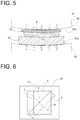
- a pressurizing tool 50 having a pressurizing board 51 having a pressurizing surface 51a of a swelling-curved surface shape and a pressurizing board 52 having a pressurizing surface 52a of a sunk-curved surface shape.
- the pressurizing surfaces 51a and 52a facing to each other be formed in a sunk surface or a swelled surface having a curved surface with a radius of curvature R 3000 mm to 7000 mm.
- the pressurizing surface 52a of the pressurizing board 52 pressing a lower surface of the heat sink 20 in the layering direction is formed by a sunk surface
- the pressing surface 51a of the pressurizing board 51 pressing an upper surface of the power-module substrate 10 (the upper surface of the circuit layer 12) in the layering direction is formed by a swelled surface.
- the pressurizing tool 50 is provided with an urging device such as a spring or the like giving a pressurizing force by urging the pressurizing boards 51 and 52 in the layering direction, though the illustration is omitted.
- flat boards can be also used for the pressurizing boards 51 and 52.
- the power-module substrate 10 and the heat sink 20 are disposed in a layered manner so that these are interposed in the layering direction.
- a layered body of the power-module substrate 10 and the heat sink 20 is pressurized in the layering direction (a thickness direction) by the pressurizing surface 51a of the pressurizing board 51 and the pressurizing surface 52a of the pressurizing board 52, and held in a state of deformation (a warp) swelling the lower surface of the heat sink 20 downward.
- the layered body of the power-module substrate 10 and the heat sink 20 is heated in the pressurized state by the pressurizing tool 50 so that the lower surface of the metal layer 13 of the power-module substrate 10 and an upper surface of the heat sink 20 (the coating layer 22) are bonded by solid-diffusion bonding.
- the solid-phase diffusion bonding is performed by maintaining in vacuum atmosphere, 0.1 MPa to 3.5 MPa of a pressurizing load (a pressurizing force), 450°C to 548°C (inclusive) of heating temperature for 5 minutes to 240 minutes. Accordingly, between the metal layer 13 of the power-module substrate 10 and the heat sink 20 (the coating layer 22), the copper atoms in the metal layer 13 and the aluminum atoms in the heat sink 20 (the coating layer 22) are mutually diffused. Thereby forming the diffusion layer 31 having the intermetallic compound of copper and aluminum between the metal layer 13 and the heat sink 20, the power-module substrate 10 and the heat sink 20 are bonded with interposing the diffusion layer 31. In addition, the thickness t131 of the diffusion layer 31 is increased in accordance with bonding time.
- the diffusion layer 31 has a structure in which intermetallic compounds with a plurality of composition in accordance with an existence ration of the aluminum atoms and the copper atoms are layered along a boundary surface between the metal layer 13 and the heat sink 20. That is to say, in an area at the heat sink 20 side of the diffusion layer 31, the existence ratio of the aluminum atoms is high, and an intermetallic compound phase with large content of aluminum is formed. On the other hand, in an area at the metal layer 13 side of the diffusion layer 31, the existence ratio of the copper atoms is high, and an intermetallic compound phase with large content of copper is formed. Accordingly, the metal layer 13 and the heat sink 20 can be adhered to each other and firmly bonded.
- the diffusion layer 31 is a part in which aluminum (Al) density is less than 90 atm% and copper (Cu) density is less than 99 atm% in a bonding boundary between the metal layer 13 and the heat sink 20.
- a vertical section of the power-module substrate with heat-sink 101 can be measured in the thickness direction of the bonding boundary between the metal layer 13 and the heat sink 20 by performing line analysis by EPMA (JXA-8530F made by JEOL Ltd.: an accelerating voltage 15 kV, a spot diameter not more than 1 ⁇ m, magnification 500-power, an interval 0.3 ⁇ m).
- a thickness of a part in which the aluminum density is less than 90 atm% and the copper (Cu) density is less than 99 atm% in the line analysis is the thickness t131 of the diffusion layer.
- a bonded body of the power-module substrate 10 and the heat sink 20 is cooled to 30°C in a state of being installed on the pressurizing tool 50, that is, in a state of being pressurized.
- the bonded body of the power-module substrate 10 and the heat sink 20 is pressurized in the thickness direction by the pressurizing tool 50 so as to be bound in a state of deformation of a warp in which the lower surface of the heat sink 20 swells downward. Therefore, a shape of the bonded body appears not to change while the cooling: however, the bonded body is restricted by being pressurized against stress into a state in which deformation as a warp by cooling cannot be accepted: as a result, plastic deformation arises.
- the pressurization of the pressurizing tool 50 is released, so that the power-module substrate with heat-sink 101 is manufactured.
- the thickness t2 of the metal layer 13 made of copper or a copper alloy having high rigidity is larger (thicker) than the thickness t1 of the circuit layer 12, resistance force of the metal layer 13 is dominant in the stress difference between the front and back (the upper and lower) surfaces of the metal layer 13. Therefore, although there is a slightly difference of the coefficient of linear expansion between the ceramic board 11 and the aluminum-impregnated silicon carbide porous body forming the heat sink 20 though, it is possible to reduce the warp resulting from the difference of the linear expansion between the ceramic board 11 and the heat sink 20. Accordingly, it is possible to reduce the warp arising in the whole body of the power-module substrate with heat-sink 101.
- the ceramic board 11 may be broken (crack) by the thermal expansion of the metal layer 13. If the thickness t1 of the circuit layer 12 is larger than the thickness t2 of the metal layer 13, the warp may arise because influence of the thermal expansion of the circuit layer 12 is large.
- the warp of the power-module substrate with heat-sink 101 is reduced by balancing the power-module substrate with heat-sink 101 as a whole, by forming the thickness t1 of the circuit layer 12 in the range of 0.1 mm to 3.0 mm (inclusive), forming the thickness t2 of the metal layer 13 to be larger than the thickness t1 and in the range of 0.15 mm to 5.0 mm (inclusive), and adjusting the relation between the circuit layer 12 and the metal layer 13 to have the ratio ⁇ ( ⁇ 2 ⁇ t2 ⁇ A2) / ( ⁇ 1 ⁇ t1 ⁇ A1) ⁇ 1.5 to 15 (inclusive).
- the value X of the warp (Z/L 2 ) when it is heated to 285°C is between -50 ⁇ 10 -6 (mm -1 ) and 50 ⁇ 10 -6 (mm -1 ) (inclusive)
- the value Y of the warp (Z/L 2 ) when it is cooled to 30°C after heating to 285°C is between -50 ⁇ 10 -6 (mm -1 ) and 50 ⁇ 10 -6 (mm -1 ) (inclusive).
- the warps X and Y exceed 50 ⁇ 10 -6 (mm -1 )
- a large amount of grease is necessary to be used between the heat sink 20 and the water-cooling cooler, and thermal resistance may be increased.
- the warps X and Y are less than -50 ⁇ 10 -6 (mm -1 )
- the heat-sink-attached board of for power module 101 is installed on the water-cooling cooler or the like, a load is placed on the ceramic board 11 and breakages or the like may arise.
- the power-module substrate with heat-sink 101 it is possible to reduce the warp arising in manufacturing the power module and reduce the warp deformation in a process of heat treatment: it is possible to improve workability in the manufacturing process such as soldering of the electronic part 30 and reliability to the hot-cold cycle load on the power module.
- the thickness t1 of the circuit layer is less than 0.1 mm, bonding material used for bonding the ceramic board 11 and the circuit layer 12 may exude to a surface of the circuit layer 12 when heated. If the thickness t1 of the circuit layer 12 is more than 3.0 mm, when the power-module substrate with heat-sink 101 is heated, for example when bonding the semiconductor element, the ceramic board 11 may be broken.
- the thickness t2 of the metal layer 13 is less than 0.15 mm, the effect of reducing the warp arising in the power-module substrate with heat-sink 101 by increasing the thickness t2 of the metal layer 13 cannot be shown. Moreover, if the thickness t2 of the metal layer 13 is more than 5.0 mm, when the power-module substrate with heat-sink 101 is heated, for example when bonding the semiconductor element, the ceramic board 11 may be broken.
- the copper boards which would be the circuit layer as shown in Table 1, used were rectangular boards made of OFC (coefficient of linear expansion 17.7 ⁇ 10 -6 K -1 , the yield stress 200 MPa) or ZC (coefficient of linear expansion: 17.7 ⁇ 10 -6 K -1 , the yield stress 270 MPa), with a plane size 37 mm ⁇ 37 mm.
- Ag-Ti based active metal brazing material was used for bonding the respective copper boards and the ceramic board: the copper boards, the active metal brazing material, and the ceramic board were layered and pressurized in the layered direction with pressurizing force 0.1 MPa and heated at heating temperature 850°C for 10 minutes so that the copper board which would be the circuit layer and the ceramic board, the copper board which would be the metal layer and the ceramic board were bonded respectively, and the power-module substrate was manufactured.
- the solid-phase diffusion bonding between the power-module substrate and the heat sink was performed as described in Table 2, using the pressurizing board having the pressurizing surface with the radius of curvature R, by pressurizing and heating with the pressurizing load 2.1 MPa and heating temperature 510°C for 150 minutes in vacuum atmosphere.
- the radius of curvature R is denoted by " ⁇ " if the pressurizing surface was a flat surface.
- the deformation amount Z was measured (1) when heated to 285°C and when (2) cooled to 30°C after heated to 285°C.
- a change of flatness at the lower surface (the back surface) of the heat sink at points of time was measured by moiré interferometry in accordance with JESD22-B112 or JEITAED-7306.
- the moiré interferometry is a method such as: by irradiating a measuring light to a measuring surface through a diffraction grating and taking a photo of scattered light scattered at the measuring surface through the diffraction grating with an imaging part so that moiré interference fringes are obtained, and measuring the deformation amount of the measuring surface in accordance with information of moiré interference fringes, a pitch of the diffraction grating and the like.
- TherMoire PS200 made by Akrometrix was used as a measuring device.
- the deformation amount Z at the lower surface of the heat sink in the measuring area E was measured with setting the center position C of the bonding surface of the heat sink 20 and the metal layer 13 as the center of the measuring area E.
- the deformation amount Z was set to be positive if the deformation projected at the circuit layer side or negative if the deformation projected at the heat sink lower surface side.
- the measuring area E is a rectangular area of W 36 mm ⁇ H 36 mm as shown in FIG. 6 and FIG. 7A : in this case, the maximum length L is a length of a diagonal line of the measuring area E.
- the deformation amount Z is a difference between a maximum value and a minimum value of measuring values on the diagonal line of the measuring area E, as shown in FIG. 7B or FIG. 7C .
- the warp (Z/L 2 ) was calculated from the deformation amount Z and the maximum length L.
- the ceramic breakage was evaluated by observation of the ceramic board with an ultrasonic flaw detector after the heating test described above: if a crack was generated in the ceramic board, it was rejected; or if the crack was not generated, it was passed.
- existence of occurrence of position displacement were checked about 30 test pieces by measuring a soldering position after soldering the electronic parts on the circuit layer. If position displacement of not less than 0.2 mm was occurred, it was rejected; or if the position displacement was less than 0.2 mm, it was passed.
- the thickness t1 is between 0.1 mm and 3.0 mm (inclusive)
- the thickness t2 is between 0.15 mm and 5.0 mm (inclusive)
- the thickness t1 is formed to be larger than the thickness t1
- the ratio ⁇ ( ⁇ 2 ⁇ t2 ⁇ A2) / ( ⁇ 1 ⁇ t1 ⁇ A1) ⁇ is in a range of 1.5 to 15 (inclusive)
- the difference (Y -X) were between -18.0 ⁇ 10 -6 (mm -1 ) and 18.0 ⁇ 10 -6 (mm -1 ).
- both the evaluation of the "ceramic breakage" and the "element-position displacement" showed good results.
Landscapes
- Engineering & Computer Science (AREA)
- Chemical & Material Sciences (AREA)
- Ceramic Engineering (AREA)
- Microelectronics & Electronic Packaging (AREA)
- Manufacturing & Machinery (AREA)
- Materials Engineering (AREA)
- Organic Chemistry (AREA)
- Structural Engineering (AREA)
- Physics & Mathematics (AREA)
- Thermal Sciences (AREA)
- Inorganic Chemistry (AREA)
- Cooling Or The Like Of Semiconductors Or Solid State Devices (AREA)
- Cooling Or The Like Of Electrical Apparatus (AREA)
- Structure Of Printed Boards (AREA)
Abstract
Description
- The present invention relates to a power-module substrate with heat-sink used for a semiconductor device controlling a large electric current and a high voltage.
- Priority is claimed on Japanese Patent Application No.
2017-42543, filed March 7, 2017 - As a power-module substrate with heat-sink, as described in Patent Document 1 or Patent Document 2 for example, known is a structure in which a circuit layer made of copper or the like is formed on one surface of a ceramic board that would be an insulating layer; a metal layer made of copper or the like is formed on the other surface of the ceramic board; and a heat sink (a heat radiation board) made of aluminum, copper, or the like is bonded on an opposite surface of the ceramic board to the metal layer. By soldering (mounting) electronic parts such as a semiconductor element and the like on a surface (an upper surface) of the circuit layer of the power-module substrate with heat-sink structured as above, a power module is manufactured.
- The heat sink made from aluminum or copper has a large difference in coefficients of linear expansion from that of the power-module substrate. Accordingly, the power-module substrate with heat-sink is warped by being heated in a mounting process of the electronic parts or exposed in temperature change in environment of using a power module. For instance, if the power-module substrate with heat-sink is warped in the mounting process of the electronic parts, a position of the electronic part may be dislocated or a bonding reliability may be deteriorated by warps or cracks in a solder-bonded part.
- Moreover, if the power-module substrate with heat-sink is warped in the environment of using the power module, thermal-electric conductive grease between the heat sink and a cooler flows out by a pump-out phenomenon, so that adhesiveness may be deteriorated between the heat sink and the cooler and thermal resistance may be increased. Furthermore, if the power-module substrate with heat-sink is warped repeatedly as above, so that the cracks may arise in the ceramic board.
- Accordingly, in such a power-module substrate with heat-sink, by forming the heat sink from an aluminum-impregnated silicon carbide porous body with low thermal expansion and high thermal conductivity instead of aluminum or copper, it is attempted to reduce the warp owing to the difference of linear expansion between the power-module substrate and the heat sink.
- The aluminum-impregnated silicon carbide porous body is, as described in Patent Document 3 or Patent Document 4, a composite body of aluminum and silicon carbide in which aluminum (Al) or an aluminum alloy is impregnated in a porous body formed from mainly silicon carbide (SiC) and a coating layer of aluminum or the aluminum alloy is formed on a surface of the porous body.
-
- Patent Document 1: Japanese Unexamined Patent Application, First Publication No.
H10-270596 - Patent Document 2: Japanese Unexamined Patent Application, First Publication No.
2016-51778 - Patent Document 3: Japanese Unexamined Patent Application, First Publication No.
2014-143351 - Patent Document 4: Japanese Unexamined Patent Application, First Publication No.
2003-306730 - As described in Patent Document 3 or Patent Document 4, it was conventionally attempted to reduce the warps of the power-module substrate with heat-sink by forming the heat sink from the aluminum-impregnated silicon carbide porous body with low thermal expansion and high thermal conductivity and reducing the difference of linear expansion between the power-module substrate and the heat sink. However, it is not enough to reduce the warp amount in the power-module substrate with heat-sink, and further improvement is required.
- The present invention is achieved in consideration of the above circumstances, and has an object to provide a power-module substrate with heat-sink having high reliability against power cycles and hot-cold cycles.
- A power-module substrate with heat-sink of the present invention includes: a power-module substrate in which a circuit layer made of copper or a copper alloy is disposed on one surface of a ceramic board and a metal layer made of copper or a copper alloy is disposed on the other surface of the ceramic board; and a heat sink which is bonded on the metal layer of the power-module substrate and formed from an aluminum-impregnated silicon carbide porous body in which aluminum or an aluminum alloy is impregnated in a porous body made of silicon carbide: in the power-module substrate with heat-sink, where yield stress of the circuit layer is σ1 (MPa), a thickness of the circuit layer is t1 (mm), and a bonding area between the circuit layer and the ceramic board is A1 (mm2) and yield stress of the metal layer is σ2 (MPa), a thickness of the metal layer is t2 (mm), and a bonding area between the metal layer and the ceramic board is A2 (mm2): in the power-module substrate with heat-sink, the thickness t1 is formed to be not less than 0.1 mm and not more than 3.0 mm, the thickness t2 is formed to be not less than 0.15 mm and not more than 5.0 mm and the thickness t2 is formed to be larger than the thickness t1, and a ratio {(σ2 × t2 × A2) / (σ1 × t1 × A1)} is in a range not less than 1.5 and not more than 15.
- The aluminum-impregnated silicon carbide porous body forming the heat sink has coefficient of liner expansion which is near to the ceramic board: there is a slightly difference in the coefficient of linear expansion. Accordingly, if the metal layer is thin, a warp arises resulting from the difference of linear expansion between the ceramic board and the heat sink.
- In the power-module substrate with heat-sink of the present invention, the thickness t2 of the metal layer made of copper or a copper alloy having high rigidity is larger (thicker) than the thickness t1 of the circuit layer; so that resistance force of the metal layer is dominant in stress difference along the front and back surfaces of the metal layer. Therefore, it is possible to reduce the warp resulting from the difference of linear expansion between the ceramic board and the heat sink, and it is possible to further reduce the warp arisen in the power-module substrate with heat-sink.
- However, if the thickness t2 of the metal layer is too large, the ceramic board may be broken (cracked) resulting from thermal expansion of the metal layer while hot-cold cycles. Moreover, if the thickness t1 of the circuit layer is larger than the thickness t2 of the metal layer, influence of thermal expansion of the circuit layer is increased, so that a warp arises. Accordingly, the circuit layer and the metal layer are formed in a range of prescribed thicknesses, and a relation between the circuit layer and the metal layer is adjusted in a range of a ratio {(σ2 × t2 × A2) / (σ1 × t1 × A1)} not less than 1.5 and not more than 15. Thereby reducing the warp of the whole of the power-module substrate with heat-sink, and it is possible to form the power-module substrate with heat-sink having high reliability against the power cycles and the hot-cold cycles.
- In addition, if the thickness t1 of the circuit layer is less than 0.1 mm, bonding material used for bonding the ceramic board and the circuit layer may exude on a surface of the circuit layer by heating. Moreover, if the thickness t1 of the circuit layer is more than 3.0 mm, in a case in which a semiconductor element is bonded or the like for example, when the power-module substrate with heat-sink is heated; the ceramic board may be cracked.
- If the thickness t2 of the metal layer is less than 0.15 mm, an effect of reducing the warp arising in the power-module substrate with heat-sink by increasing the thickness t2 of the metal layer cannot be shown. Moreover, if the thickness t2 of the metal layer is more than 5.0 mm, when the power-module substrate with heat-sink is heated, for example when bonding the semiconductor element, the ceramic board may be cracked.
- As a preferred aspect of the power-module substrate with heat-sink of the present invention, on a lower surface of the heatsink, a center position of a bonding surface between the heat sink and the metal layer is set to be a center of a measuring area, a maximum length of the measuring area is set to L (mm), a deformation amount of the heat sink in the measuring area is set to Z (mm), a value of a warp (Z/L2) when heated to 285°C is set to X, and a value of a warp (Z/L2) when cooled to 30°C after heated to 285°C is set to Y: a difference (Y - X) between the warp X and the warp Y is not less than -18.0 × 10⁻⁶ (nim-1) and not more than 18.0 × 10⁻⁶ (mm-1). Here, the deformation amount Z is positive if the deformation swells toward the circuit layer side; or negative if the deformation swells toward the lower surface side of the heat sink.
- In the power-module substrate with heat-sink in which the difference (Y - X) between the warp X when heated 285°C and the warp Y when cooled 30°C from 285°C after the heating is between -18.0 × 10⁻⁶ (nim-1) and 18.0 × 10⁻⁶ (nim-1) (inclusive), the difference between the warps arising at the low temperature (30°C) and the high temperature (285°C) is also small. In such a power-module substrate with heat-sink, the warp arising when soldering the electronic part on the circuit layer or wire-bonding or the like and the warp arising when the load of the hot-cold cycles of the power module is placed on are small: it is possible to improve workability in the manufacturing process such as soldering of the electronic part and the like, and to prevent the ceramic board from cracking.
- As a preferred aspect of the power-module substrate with heat-sink of the present invention, it is preferable that the warp X be not less than -50 × 10-6 (mm-1) and not more than 50 × 10-6 (nim-1) and the warp Y be not less than -50 × 10-6 (mm-1) and not more than 50 × 10-6 (mm-1).
- In a case in which the warps X and Y are more than 50 × 10-6 (mm-1), when the power-module substrate with heat-sink is installed on a water-cooling cooler oar the like, a large amount of grease is necessary to be used between the heat sink and the water-cooling cooler, and thermal resistance may be increased. In a case in which the warps X and Y are less than -50 × 10-6 (mm-1), when the power-module substrate with heat-sink is installed on the water-cooling cooler or the like, a load is placed on the ceramic board and cracks or the like may arise.
- As a preferred aspect of the power-module substrate with heat-sink of the present invention, it is preferable that a diffusion layer having an intermetallic compound of aluminum and copper be formed between the metal layer and the heat sink.
- Between the metal layer of the power-module substrate and the heat sink, the diffusion layer having the intermetallic compound of aluminum and copper is formed and the metal layer and the heat sink are bonded with the diffusion layer therebetween; so that the metal layer and the heat sink are closely adhered to each other and can be firmly bonded.
- According to the power-module substrate with heat-sink of the present invention, it is possible to prevent the ceramic board from cracking resulting from the temperature variation and the reliability against the power cycles and the hot-cold cycles can be improved.
-
- [
FIG. 1 ] It is a sectional view showing a power-module substrate with heat-sink of the present invention. - [
FIG. 2 ] It is a perspective view of a power-module substrate. - [
FIG. 3 ] It is a sectional view of an essential part of a heat sink. - [
FIG. 4 ] It is a view explaining a part of a manufacturing method of the power-module substrate with heat-sink shown inFIG. 1 and is a sectional view explaining a manufacturing process of a power-module substrate. - [
FIG. 5 ] It is a view explaining a part of the manufacturing method of the power-module substrate with heat-sink shown inFIG. 1 and is a sectional view showing a bonding step of the power-module substrate and a heat sink. - [
FIG. 6 ] It is a schematic view explaining a measuring area of a warp and is a plan view of a lower surface of the heat sink of the power-module substrate with heat-sink. - [
FIG. 7A ] It is a schematic view explaining a measuring method of the warp and shows a plan view of the measuring area. - [
FIG. 7B ] It is a sectional view on a diagonal line of the measuring area when the warp is positive in the measuring area shown inFIG. 7A . - [
FIG. 7C ] It is a sectional view on the diagonal line of the measuring area when the warp is negative in the measuring area shown inFIG. 7A . - Below, an embodiment of the present invention will be explained with referring the drawings. A power-module substrate with heat-
sink 101 of the present embodiment is shown inFIG. 1 . The power-module substrate with heat-sink 101 is provided with a power-module substrate 10 and aheat sink 20 bonded on the power-module substrate 10. - As shown in
FIG. 2 , the power-module substrate 10 is provided with aceramic board 11 structuring an insulating layer, acircuit layer 12 disposed on one surface (an upper surface inFIG. 1 ) of theceramic board 11, and ametal layer 13 disposed on the other surface (a lower surface inFIG. 1 ) of theceramic board 11. - The
ceramic board 11 is for preventing electric connection between thecircuit layer 12 and themetal layer 13. Theceramic board 11 is formed from ceramics having high insulation, for instance, such as A1N (aluminum nitride), Si3N4 (silicon nitride), Al2O3 (alumina), SiC (silicon carbide), to have a thickness t3 in a range of not less than 0.32 mm and not more than 1.0 mm. - The
circuit layer 12 is formed by bonding a copper board made of copper or a copper alloy (preferably oxygen-free copper: OFC) on one surface of theceramic board 11. Thecircuit layer 12 has a prescribed circuit pattern formed by etching or the like. The circuit layer 12 (a thickness of the copper board) has the thickness t1 in a range of not less than 0.1 mm and not more than 3.0 mm. - The
metal layer 13 is formed by bonding a copper board made of copper or a copper alloy (preferably oxygen-free copper: OFC) on the other surface of theceramic board 11. A thickness t2 of the metal layer 13 (a thickness of the copper board) is formed in a range not less than 0.15 mm and not more than 5.0 mm. - In the power-
module substrate 10, as shown inFIG. 2 , where yield strength of thecircuit layer 12 is σ1 (MPa), the thickness of thecircuit layer 12 is t1 (mm), a bonding area between thecircuit layer 12 and theceramic board 11 is A1 (mm2); and yield strength of themetal layer 13 is σ2 (MPa), the thickness of themetal layer 13 is t2 (mm), a bonding area between themetal layer 13 and theceramic board 11 is A2 (mm2); the thickness t2 of themetal layer 13 is formed to be larger (thicker) than the thickness t1 of the circuit layer, and thecircuit layer 12 and themetal layer 13 are adjusted to have a relation in which a ratio {(σ2 × t2 × A2) / (σ1 × t1 × A1)} is in a range between 1.5 and 15 inclusive. - In addition, a circuit pattern is formed in the circuit layer 12: in a case in which it has a plurality of separated pattern forms, the bonding area A1 (mm2) is a total sum of bonding areas of the respective pattern forms: the bonding area A1 of the
circuit layer 12 is normally an area of about 90% of the bonding area A2 of themetal layer 13. The yield strength σ1 of thecircuit layer 12 and the yield strength σ2 of themetal layer 13 are yield strengths at 25°C of a conditioning (temper) designation "O". - The
heat sink 20 is for cooling the power-module substrate 10. Theheat sink 20 is bonded on a lower surface of themetal layer 13, as shown inFIG. 1 . As shown inFIG. 3 , theheat sink 20 is formed from an aluminum-impregnated silicon carbide porous body in which aluminum (Al) or an aluminum alloy is impregnated in a porous body 21 made of silicon carbide (SiC); andcoating layers 22 of aluminum or the aluminum alloy which is impregnated inside are formed on a surface of the porous body 21: and theheat sink 20 is formed as a flat board shape. - For the aluminum which is impregnated in the porous body 21 of the
heat sink 20, pure aluminum as exemplified by aluminum (2N-A1) of purity 99% or higher by mass and aluminum (4N-A1) of purity 99.99% by mass, or an aluminum alloy having composition below can be used: Al: between 80% by mass and 99.99% by mass inclusive, Si: between 0.01 % by mass and 12.6% by mass inclusive, Mg: between 0.03% by mass and 5.0% by mass inclusive, and the remainder: impurity. Aluminum alloys such asADC 12, A356 and the like can be also used. - A thickness t4 of the
heat sink 20 can be 0.5 mm to 5.0 mm inclusive. The thickness t4 of theheat sink 20 is a thickness including a thickness t141 of the coating layers 22 coating both the surfaces of the porous body 21. The thickness t141 per one surface of the coating layers 22 is preferably 0.01-fold to 0.1-fold (inclusive) of the thickness t4 of theheat sink 20. - The
heat sink 20 in which the coating layers 22 are formed on the surfaces of the porous body 21 is manufactured by, for example, disposing the porous body 21 in a mold which is provided so as to have a prescribed clearance on a periphery thereof in advance, press-injecting heated and melted aluminum or the aluminum alloy in the mold, and cooling them in a pressurized state. As described above, by press-injecting aluminum or the like, the aluminum alloy can be impregnated in the porous body 21 which has bad wettability with aluminum and the like; furthermore, aluminum or the like is filled in the clearance around the porous body 21 so that the coating layers 22 having the prescribed thickness can be formed on the surface of the porous body 21. In addition, the thickness 1141 of the coating layers 22 may be adjusted by cutting of the coating layers 22 which are already formed. - Between the
metal layer 13 of the power-module substrate 10 and theheat sink 20, adiffusion layer 31 having an intermetallic compound consisting of copper and aluminum is formed by mutually diffusion of copper atoms in themetal layer 13 and aluminum atoms in theheat sink 20. It is preferable to form a thickness t131 of thediffusion layer 31 be in a range between 2 µm and 50 µm (inclusive) in a range of the thickness t141 of the coating layers 22. - In addition, as a preferable example of combination of the power-module substrate with heat-
sink 101 of the present embodiment, respective members of the power-module substrate 10 are structured from, for example, theceramic board 11 is A1N (aluminum nitride) with the thickness t3 = 0.635 mm, and themetal layer 13 is OFC (oxygen-free copper, the yield strength σ1 : 200 MPa) with the thickness t2 = 2.0 mm. In a case in which the bonding area A1 is 1369 mm2 and the bonding area A2 is 1369 mm2, the ratio {(σ2 × t2 × A2) / (σ1 × t1 × A1)} = 8.21. In theheat sink 20, the aluminum or the like which is impregnated is structured from an Al-Si based alloy, the whole thickness t4 is 5.0 mm, and the coating layers 22 is structured with the thickness t141 about 100 µm. The thickness t131 of thediffusion layer 31 is about 25 µm. - In addition, coefficients of linear expansion of the respective members are as follows: 4.5 × 10⁻⁶ K-1 for the
ceramic board 11 made of AlN; 17.7 × 10⁻⁶ K-1 for thecircuit layer 12 and themetal layer 13 made of OFC; and 8.5 × 10⁻⁶ K-1 for theheat sink 20 made of the aluminum-impregnated silicon carbide porous body into which an Al-Si based alloy is impregnated. - On an upper surface of the
circuit layer 12 in the power-module substrate with heat-sink 101 structured as above, anelectronic part 30 such as a semiconductor element or the like is mounted so that apower module 201 is manufactured as shown inFIG. 1 . Theelectronic part 30 is solder-bonded on the upper surface of thecircuit layer 12 by solder material such as Sn-Cu, Sn-Cu-Ni or the like: a solder-bonding part with a thickness about 50 µm to 200 µm is formed between theelectronic part 30 and thecircuit layer 12, though the illustration is omitted. - Below, a manufacturing process of the power-module substrate with heat-
sink 101 of the present embodiment will be explained. - First, a copper board which will be the
circuit layer 12 and theceramic board 11, and a copper board which will be themetal layer 13 and theceramic board 11, are bonded. The bonding of the copper boards which will be thecircuit layer 12 and themetal layer 13 to theceramic board 11 is performed by a so-called active-metal brazing method. - In detail, the copper board which will be the
circuit layer 12 is layered on the upper surface of theceramic board 11 with interposing the active metal brazing material of Ag-Cu-Ti, Ag-Ti or the like (not illustrated): and the copper board which will be themetal layer 13 is layered on the lower surface of theceramic board 11 with interposing the same active metal brazing material. Then, a layered body in which these copper boards, the active metal brazing material, and theceramic board 11 is heated in a pressured state in a layering direction thereof in a range between 0.1 MPa and 3.5 MPa (inclusive) as shown inFIG. 4 , so that the copper board which will be thecircuit layer 12 is bonded to theceramic board 11, and the copper board which will be themetal layer 13 is bonded to the ceramic board 11: then, the power-module substrate 10 is manufactured. Heating condition for this, heating temperature is 850°C and heating time is 10 minutes, for example. - Next, the
heat sink 20 is bonded on the lower surface of themetal layer 13 of the power-module substrate 10. For bonding the power-module substrate 10 and theheat sink 20, as shown inFIG. 5 , it is preferable to use apressurizing tool 50 having a pressurizingboard 51 having a pressurizingsurface 51a of a swelling-curved surface shape and a pressurizingboard 52 having a pressurizingsurface 52a of a sunk-curved surface shape. For the two pressurizingboards FIG. 5 , the pressurizingsurface 52a of the pressurizingboard 52 pressing a lower surface of theheat sink 20 in the layering direction is formed by a sunk surface, and thepressing surface 51a of the pressurizingboard 51 pressing an upper surface of the power-module substrate 10 (the upper surface of the circuit layer 12) in the layering direction is formed by a swelled surface. The pressurizingtool 50 is provided with an urging device such as a spring or the like giving a pressurizing force by urging the pressurizingboards boards - Between the pressurizing
board 51 and the pressurizingboard 52 of the pressurizingtool 50 structured as above, the power-module substrate 10 and theheat sink 20 are disposed in a layered manner so that these are interposed in the layering direction. At this time, a layered body of the power-module substrate 10 and theheat sink 20 is pressurized in the layering direction (a thickness direction) by the pressurizingsurface 51a of the pressurizingboard 51 and the pressurizingsurface 52a of the pressurizingboard 52, and held in a state of deformation (a warp) swelling the lower surface of theheat sink 20 downward. The layered body of the power-module substrate 10 and theheat sink 20 is heated in the pressurized state by the pressurizingtool 50 so that the lower surface of themetal layer 13 of the power-module substrate 10 and an upper surface of the heat sink 20 (the coating layer 22) are bonded by solid-diffusion bonding. - In this case, the solid-phase diffusion bonding is performed by maintaining in vacuum atmosphere, 0.1 MPa to 3.5 MPa of a pressurizing load (a pressurizing force), 450°C to 548°C (inclusive) of heating temperature for 5 minutes to 240 minutes. Accordingly, between the
metal layer 13 of the power-module substrate 10 and the heat sink 20 (the coating layer 22), the copper atoms in themetal layer 13 and the aluminum atoms in the heat sink 20 (the coating layer 22) are mutually diffused. Thereby forming thediffusion layer 31 having the intermetallic compound of copper and aluminum between themetal layer 13 and theheat sink 20, the power-module substrate 10 and theheat sink 20 are bonded with interposing thediffusion layer 31. In addition, the thickness t131 of thediffusion layer 31 is increased in accordance with bonding time. - The
diffusion layer 31 has a structure in which intermetallic compounds with a plurality of composition in accordance with an existence ration of the aluminum atoms and the copper atoms are layered along a boundary surface between themetal layer 13 and theheat sink 20. That is to say, in an area at theheat sink 20 side of thediffusion layer 31, the existence ratio of the aluminum atoms is high, and an intermetallic compound phase with large content of aluminum is formed. On the other hand, in an area at themetal layer 13 side of thediffusion layer 31, the existence ratio of the copper atoms is high, and an intermetallic compound phase with large content of copper is formed. Accordingly, themetal layer 13 and theheat sink 20 can be adhered to each other and firmly bonded. - The
diffusion layer 31 is a part in which aluminum (Al) density is less than 90 atm% and copper (Cu) density is less than 99 atm% in a bonding boundary between themetal layer 13 and theheat sink 20. For instance, a vertical section of the power-module substrate with heat-sink 101 can be measured in the thickness direction of the bonding boundary between themetal layer 13 and theheat sink 20 by performing line analysis by EPMA (JXA-8530F made by JEOL Ltd.: an accelerating voltage 15 kV, a spot diameter not more than 1 µm, magnification 500-power, an interval 0.3 µm). A thickness of a part in which the aluminum density is less than 90 atm% and the copper (Cu) density is less than 99 atm% in the line analysis is the thickness t131 of the diffusion layer. - Next, a bonded body of the power-
module substrate 10 and theheat sink 20 is cooled to 30°C in a state of being installed on the pressurizingtool 50, that is, in a state of being pressurized. In this case, the bonded body of the power-module substrate 10 and theheat sink 20 is pressurized in the thickness direction by the pressurizingtool 50 so as to be bound in a state of deformation of a warp in which the lower surface of theheat sink 20 swells downward. Therefore, a shape of the bonded body appears not to change while the cooling: however, the bonded body is restricted by being pressurized against stress into a state in which deformation as a warp by cooling cannot be accepted: as a result, plastic deformation arises. Then, after cooling to 30°C, the pressurization of the pressurizingtool 50 is released, so that the power-module substrate with heat-sink 101 is manufactured. - In the power-module substrate with heat-
sink 101, since the thickness t2 of themetal layer 13 made of copper or a copper alloy having high rigidity is larger (thicker) than the thickness t1 of thecircuit layer 12, resistance force of themetal layer 13 is dominant in the stress difference between the front and back (the upper and lower) surfaces of themetal layer 13. Therefore, although there is a slightly difference of the coefficient of linear expansion between theceramic board 11 and the aluminum-impregnated silicon carbide porous body forming theheat sink 20 though, it is possible to reduce the warp resulting from the difference of the linear expansion between theceramic board 11 and theheat sink 20. Accordingly, it is possible to reduce the warp arising in the whole body of the power-module substrate with heat-sink 101. - However, if the thickness t2 of the
metal layer 13 is too large, when the power-module substrate with heat-sink 101 is heated, for example, when the semiconductor element and the like is bonded, theceramic board 11 may be broken (crack) by the thermal expansion of themetal layer 13. If the thickness t1 of thecircuit layer 12 is larger than the thickness t2 of themetal layer 13, the warp may arise because influence of the thermal expansion of thecircuit layer 12 is large. - Accordingly, in the power-module substrate with heat-
sink 101 of the present embodiment, the warp of the power-module substrate with heat-sink 101 is reduced by balancing the power-module substrate with heat-sink 101 as a whole, by forming the thickness t1 of thecircuit layer 12 in the range of 0.1 mm to 3.0 mm (inclusive), forming the thickness t2 of themetal layer 13 to be larger than the thickness t1 and in the range of 0.15 mm to 5.0 mm (inclusive), and adjusting the relation between thecircuit layer 12 and themetal layer 13 to have the ratio {(σ2 × t2 × A2) / (σ1 × t1 × A1)} 1.5 to 15 (inclusive). - In the power-module substrate with heat-
sink 101 structured as above, on the lower surface (the back surface) of theheat sink 20, as shown inFIG. 6 andFIGS. 7A to 7C , where a center C of a bonding surface of theheat sink 20 and themetal layer 13 is set as a center of a measuring area E, a longest length in the measuring area E is set to L, a deformation amount of the warp of theheat sink 20 in the measuring area E is set to Z, and where a value of a warp (Z/L2) when it is heated to 285°C is X and a value of a warp (Z/L2) when it is cooled after heated to 285°C is Y; a difference (Y - X) between the warp X and the warp Y is not less than -18.0 × 10⁻⁶ (mm-1) and not more than 18.0 × 10⁻⁶ (mm-1): the deformation amount of warp between at high temperature (285°C) and low temperature (30°C) can be reduced. Here, the deformation amount Z of theheat sink 20 is positive if the deformation swells toward the circuit layer side, or negative if the deformation swells toward the lower surface side of theheat sink 20. - In the power-module substrate with heat-
sink 101, the value X of the warp (Z/L2) when it is heated to 285°C is between -50 × 10-6 (mm-1) and 50 × 10-6 (mm-1) (inclusive), and the value Y of the warp (Z/L2) when it is cooled to 30°C after heating to 285°C is between -50 × 10-6 (mm-1) and 50 × 10-6 (mm-1) (inclusive). - In a case in which the warps X and Y exceed 50 × 10-6 (mm-1), when the power-module substrate with heat-
sink 101 is installed on a water-cooling cooler or the like, a large amount of grease is necessary to be used between theheat sink 20 and the water-cooling cooler, and thermal resistance may be increased. If the warps X and Y are less than -50 × 10-6 (mm-1), when the heat-sink-attached board of forpower module 101 is installed on the water-cooling cooler or the like, a load is placed on theceramic board 11 and breakages or the like may arise. - As explained above, in the power-module substrate with heat-
sink 101, it is possible to reduce the warp arising in manufacturing the power module and reduce the warp deformation in a process of heat treatment: it is possible to improve workability in the manufacturing process such as soldering of theelectronic part 30 and reliability to the hot-cold cycle load on the power module. - If the thickness t1 of the circuit layer is less than 0.1 mm, bonding material used for bonding the
ceramic board 11 and thecircuit layer 12 may exude to a surface of thecircuit layer 12 when heated. If the thickness t1 of thecircuit layer 12 is more than 3.0 mm, when the power-module substrate with heat-sink 101 is heated, for example when bonding the semiconductor element, theceramic board 11 may be broken. - If the thickness t2 of the
metal layer 13 is less than 0.15 mm, the effect of reducing the warp arising in the power-module substrate with heat-sink 101 by increasing the thickness t2 of themetal layer 13 cannot be shown. Moreover, if the thickness t2 of themetal layer 13 is more than 5.0 mm, when the power-module substrate with heat-sink 101 is heated, for example when bonding the semiconductor element, theceramic board 11 may be broken. - The present invention is not limited to the above-mentioned embodiment and various modifications may be made without departing from the scope of the present invention.
- Below, Examples for confirming the effect of the present invention will be explained. As described in Table 1, manufactured were boards for power module with varying the material of the circuit layer (the yield strength σ1) and the thickness t1 and the bonding area A1 of the circuit layer, and the material of the metal layer (the yield strength σ2) and the thickness t2 and the bonding area A2 of the metal layer. The metal layers of the respective boards for power module and the heat sinks were solid-diffusion phase bonded, so that manufactured were samples of the heat-sink-attached boards for power module in which the diffusion layer was formed between the metal layer and the heat sink.
- As the copper boards which would be the circuit layer, as shown in Table 1, used were rectangular boards made of OFC (coefficient of linear expansion 17.7 × 10⁻⁶ K-1, the yield stress 200 MPa) or ZC (coefficient of linear expansion: 17.7 × 10⁻⁶ K-1, the yield stress 270 MPa), with a plane size 37 mm × 37 mm. As the copper boards which would be the metal layer, used were rectangular boards made of OFC (coefficient of linear expansion 17.7 × 10⁻⁶ K-1, the yield stress 200 MPa) or ZC (coefficient of linear expansion: 17.7 × 10⁻⁶ K-1, the yield stress 270 MPa), with a plane size 37 mm × 37 mm. Rectangular boards with the thickness t3 = 0.635 mm and a plane size 40 mm × 40 mm made of AlN (coefficient of linear expansion 4.5 × 10⁻⁶ K-1) were used as the ceramic boards.
- Ag-Ti based active metal brazing material was used for bonding the respective copper boards and the ceramic board: the copper boards, the active metal brazing material, and the ceramic board were layered and pressurized in the layered direction with pressurizing force 0.1 MPa and heated at heating temperature 850°C for 10 minutes so that the copper board which would be the circuit layer and the ceramic board, the copper board which would be the metal layer and the ceramic board were bonded respectively, and the power-module substrate was manufactured.
- The bonding area A1 and the bonding area A2 in Table 2 are values respectively calculated from the plane sizes of the copper boards which would be the circuit layer or the metal layer: using these values, the ratio S = {(σ2 × t2 × A2) / (σ1 × t1 × A1)} was calculated.
- Used for the heat sink was a rectangular board with the whole thickness t4 =5.0 mm and the
plane size 50 mm × 60 mm formed from the aluminum-impregnated silicon carbide porous body in which the Al-Si based alloy was impregnated into silicon carbide (SiC), and formed to have the thickness t141 of the coating layers on the front and back surface were 100 µm. Then, the solid-phase diffusion bonding between the power-module substrate and the heat sink was performed as described in Table 2, using the pressurizing board having the pressurizing surface with the radius of curvature R, by pressurizing and heating with the pressurizing load 2.1 MPa and heating temperature 510°C for 150 minutes in vacuum atmosphere. In addition, the radius of curvature R is denoted by "∞" if the pressurizing surface was a flat surface. - Samples of the power-module substrate with heat-sink were obtained, and evaluated regarding the "deformation amount Z", "ceramic breakage", and "element-position displacement" respectively.
- The deformation amount Z was measured (1) when heated to 285°C and when (2) cooled to 30°C after heated to 285°C. A change of flatness at the lower surface (the back surface) of the heat sink at points of time was measured by moiré interferometry in accordance with JESD22-B112 or JEITAED-7306.
- The moiré interferometry is a method such as: by irradiating a measuring light to a measuring surface through a diffraction grating and taking a photo of scattered light scattered at the measuring surface through the diffraction grating with an imaging part so that moiré interference fringes are obtained, and measuring the deformation amount of the measuring surface in accordance with information of moiré interference fringes, a pitch of the diffraction grating and the like. TherMoire PS200 made by Akrometrix was used as a measuring device.
- In the present examples, as shown in
FIG. 6 , the deformation amount Z at the lower surface of the heat sink in the measuring area E (refer toFIG. 7A to FIG. 7C ) was measured with setting the center position C of the bonding surface of theheat sink 20 and themetal layer 13 as the center of the measuring area E. The deformation amount Z was set to be positive if the deformation projected at the circuit layer side or negative if the deformation projected at the heat sink lower surface side. - The measuring area E is a rectangular area of W 36 mm × H 36 mm as shown in
FIG. 6 andFIG. 7A : in this case, the maximum length L is a length of a diagonal line of the measuring area E. The deformation amount Z is a difference between a maximum value and a minimum value of measuring values on the diagonal line of the measuring area E, as shown inFIG. 7B or FIG. 7C . The warp (Z/L2) was calculated from the deformation amount Z and the maximum length L. - The ceramic breakage was evaluated by observation of the ceramic board with an ultrasonic flaw detector after the heating test described above: if a crack was generated in the ceramic board, it was rejected; or if the crack was not generated, it was passed. Regarding the element-position displacements, existence of occurrence of position displacement were checked about 30 test pieces by measuring a soldering position after soldering the electronic parts on the circuit layer. If position displacement of not less than 0.2 mm was occurred, it was rejected; or if the position displacement was less than 0.2 mm, it was passed.
- In the evaluation of the 30 test pieces, if a rate of being passed was not less than 90%, it was evaluated as "good": or if the rate of being passed was less than 90%, it was evaluated as "poor". Results are shown in Table 3.
[Table 1] Test Piece No. Ceramic Board Circuit Layer Metal Layer Material Thickness t3 (mm) Thickness t1 (mm) Bonding Area A1 (mm2) Material Yield Strength σ1 (MPa) Thickness t2 (mm) Bonding Area A2 (mm2) Material Yield Strength σ2 (MPa) 1 AlN 0.635 0.3 1369 OFC 200 0.45 1369 OFC 200 2 AlN 0.635 0.3 1369 OFC 200 1.00 1369 OFC 200 3 AlN 0.635 0.3 1369 OFC 200 2.00 1369 OFC 200 4 AlN 0.635 0.3 1369 OFC 200 3.00 1369 OFC 200 5 AlN 0.635 0.5 1369 OFC 200 5.00 1369 OFC 200 6 AlN 0.635 0.1 1369 OFC 200 0.50 1369 OFC 200 7 AlN 0.635 3.0 1369 OFC 200 5.00 1369 OFC 200 8 AlN 0.635 0.2 1369 OFC 200 3.00 1369 OFC 200 9 AlN 0.635 0.3 1261 ZC 270 2.00 1369 OFC 200 10 AlN 0.635 0.3 1369 OFC 200 2.00 1369 OFC 200 11 Al2O3 0.635 0.3 1369 OFC 200 2.00 1369 OFC 200 12 Si3N4 0.32 0.3 1369 OFC 200 2.00 1369 OFC 200 13 AlN 0.635 0.3 1369 OFC 200 2.00 1369 OFC 200 14 AlN 0.635 0.3 1369 OFC 200 2.00 1369 OFC 200 15 AlN 0.635 0.3 1369 OFC 200 0.30 1369 OFC 200 16 AlN 0.635 0.3 1369 OFC 200 5.00 1369 OFC 200 17 AlN 0.635 0.5 1369 OFC 200 7.00 1369 OFC 200 18 AlN 0.635 4.0 1369 OFC 200 7.00 1369 OFC 200 19 AlN 0.635 0.1 1369 OFC 200 2.00 1369 OFC 200 [Table 2] Test Piece No. Radius of Curvature R (mm) Ratio S 1 3000 1.50 2 3000 3.33 3 3000 6.67 4 3000 10.00 5 3000 10.00 6 3000 5.00 7 3000 1.67 8 3000 15.00 9 3000 5.36 10 3000 6.67 11 3000 6.67 12 3000 6.67 13 7000 6.67 14 ∞ 6.67 15 3000 1.00 16 3000 16.67 17 3000 14.00 18 3000 1.75 19 3000 20.00 [Table 3] Test Piece No. Warp (Z/L2) [× 10-6(mm-1)] Ceramic Breakage Element-Position Displacement 285°C Heated (X) 30°C Cooled (Y) Difference (Y - X) 1 21.3 38.5 17.2 GOOD GOOD 2 20.6 31.2 10.6 GOOD GOOD 3 19.2 17.9 -1.3 GOOD GOOD 4 17.8 4.5 -13.3 GOOD GOOD 5 12.2 0.2 -12.0 GOOD GOOD 6 11.0 25.0 14.0 GOOD GOOD 7 19.5 15.8 -3.7 GOOD GOOD 8 19.0 2.8 -16.2 GOOD GOOD 9 15.1 18.2 3.1 GOOD GOOD 10 14.5 11.8 -2.7 GOOD GOOD 11 23.9 22.0 -1.9 GOOD GOOD 12 33.2 27.0 -6.2 GOOD GOOD 13 32.1 31.3 -0.8 GOOD GOOD 14 57.4 55.5 -1.9 GOOD GOOD 15 23.0 42.0 19.0 GOOD POOR 16 13.8 -21.1 -34.9 GOOD POOR 17 27.6 -0.3 -27.9 POOR POOR 18 27.8 22.2 -5.6 POOR GOOD 19 -6.2 -28.7 -22.5 GOOD POOR - As recognized from Tables 1 to 3, regarding Nos. 2 to 14 in which the thickness t1 is between 0.1 mm and 3.0 mm (inclusive), the thickness t2 is between 0.15 mm and 5.0 mm (inclusive), the thickness t1 is formed to be larger than the thickness t1, and the ratio {(σ2 × t2 × A2) / (σ1 × t1 × A1)} is in a range of 1.5 to 15 (inclusive), the difference (Y -X) were between -18.0 × 10⁻⁶ (mm-1) and 18.0 × 10⁻⁶ (mm-1). In these Nos. 1 to 14, both the evaluation of the "ceramic breakage" and the "element-position displacement" showed good results.
- On the other hand, regarding Nos. 15, 16 and 19 in which the ratio {(σ2 × t2 × A2) / (σ1 × t1 × A1)} was out of the above-described range, the difference (Y - X) was deviated from the range between -18 × 10-6 (mm-1) and 18 × 10-6 (mm-1) (inclusive), the deformation amount of the warp was large, and the "element-position dislocation" arose. Regarding the test pieces of No. 17 in which the thickness t2 is larger than 5.0 mm, the deformation amount of the warp was large, and the test pieces in which the breakage of the ceramic board arose after heated to 285°C was recognized. In No. 18 in which the thickness t1 is larger than 3.0 mm and the thickness t2 is larger than 5.0 mm, although the deformation amount of the warp is small, there was a test piece in which the ceramic board was broken after heated to 285°C.
- It is possible to reduce the breakage of the ceramic board resulting from the temperature variation, and the reliability to the power cycles and the hot-cold cycles can be improved.
-
- 10
- Power-module substrate
- 11
- Ceramic board
- 12
- Circuit layer
- 13
- Metal layer
- 20
- Heat sink
- 21
- Porous body
- 22
- Coating layer
- 30
- Electronic part
- 50
- Pressurizing tool
- 51, 52
- Pressurizing board
- 101
- Power-module substrate with heat-sink
- 201
- Power module
Claims (4)
- A power-module substrate with heat-sink, comprising:a power-module substrate in which a circuit layer made of copper or a copper alloy is disposed on one surface of a ceramic board and a metal layer made of copper or a copper alloy is disposed on the other surface of the ceramic board; anda heat sink which is bonded on the metal layer of the power-module substrate and formed from an aluminum-impregnated silicon carbide porous body in which aluminum or an aluminum alloy is impregnated in a porous body made of silicon carbide, whereinwhere yield stress of the circuit layer is σ1 (MPa), a thickness of the circuit layer is t1 (mm), and a bonding area between the circuit layer and the ceramic board is A1 (mm2) and yield stress of the metal layer is σ2 (MPa), a thickness of the metal layer is t2 (mm), and a bonding area between the metal layer and the ceramic board is A2 (mm2); whereinthe thickness t1 is formed to be not less than 0.1 mm and not more than 3.0 mm,the thickness t2 is formed to be not less than 0.15 mm and not more than 5.0 mm and the thickness t2 is formed to be larger than the thickness t1, anda ratio {(σ2 × t2 × A2) / (σ1 × t1 × A1)} is in a range not less than 1.5 and not more than 15.
- The power-module substrate with heat-sink according to Claim 1, wherein, on a lower surface of the heatsink, a center position of a bonding surface between the heat sink and the metal layer is set to be a center of a measuring area,
a maximum length of the measuring area is set to L (mm),
a deformation amount of the heat sink in the measuring area is set to Z (mm),
a warp (Z/L2) when heated to 285°C is set to X, and
a warp (Z/L2) when cooled to 30°C after heated to 285°C is set to Y, wherein
a difference (Y - X) between the warp X and the warp Y is not less than -18.0 × 10⁻⁶ (mm-1) and not more than 18.0 × 10⁻⁶ (mm-1) . - The power-module substrate with heat-sink according to Claim 2, wherein the warp X is not less than -50 × 10-6 (nim-1) and not more than 50 × 10-6 (nim-1) and the warp Y is not less than -50 × 10-6 (mm-1) and not more than 50 × 10-6 (mm-1).
- The power-module substrate with heat-sink according to Claim 1, wherein a diffusion layer having an intermetallic compound of aluminum and copper is formed between the metal layer and the heat sink.
Applications Claiming Priority (2)
| Application Number | Priority Date | Filing Date | Title |
|---|---|---|---|
| JP2017042543A JP6776953B2 (en) | 2017-03-07 | 2017-03-07 | Board for power module with heat sink |
| PCT/JP2018/006746 WO2018163865A1 (en) | 2017-03-07 | 2018-02-23 | Power module substrate with heat sink |
Publications (3)
| Publication Number | Publication Date |
|---|---|
| EP3595003A1 true EP3595003A1 (en) | 2020-01-15 |
| EP3595003A4 EP3595003A4 (en) | 2021-03-17 |
| EP3595003B1 EP3595003B1 (en) | 2025-05-07 |
Family
ID=63448127
Family Applications (1)
| Application Number | Title | Priority Date | Filing Date |
|---|---|---|---|
| EP18764394.5A Active EP3595003B1 (en) | 2017-03-07 | 2018-02-23 | Power module substrate with heat sink |
Country Status (7)
| Country | Link |
|---|---|
| US (1) | US11462456B2 (en) |
| EP (1) | EP3595003B1 (en) |
| JP (1) | JP6776953B2 (en) |
| KR (1) | KR102538201B1 (en) |
| CN (1) | CN110383469B (en) |
| TW (1) | TWI750332B (en) |
| WO (1) | WO2018163865A1 (en) |
Families Citing this family (9)
| Publication number | Priority date | Publication date | Assignee | Title |
|---|---|---|---|---|
| DE102017205813A1 (en) * | 2017-04-05 | 2018-10-11 | Mahle International Gmbh | A method of manufacturing a cooling device, a cooling device and a cooling arrangement |
| JP7363613B2 (en) | 2020-03-13 | 2023-10-18 | 三菱マテリアル株式会社 | Insulated circuit board with integrated heat sink |
| CN111755413A (en) * | 2020-07-07 | 2020-10-09 | 深圳基本半导体有限公司 | A high thermal conductivity silicon carbide device packaging structure and method |
| CN113658871B (en) * | 2021-06-27 | 2024-08-02 | 厦门芯光润泽科技有限公司 | Manufacturing method of power module |
| DE102021132945B4 (en) * | 2021-12-14 | 2026-04-30 | Rogers Germany Gmbh | Carrier substrate for electrical components and methods for producing such a carrier substrate |
| EP4539118A1 (en) * | 2023-05-22 | 2025-04-16 | LX Semicon Co., Ltd. | A manufacturing method of a heat dissipation substrate for a power semiconductor module, and a manufacturing method of a power semiconductor module including the same |
| EP4538252A1 (en) * | 2023-05-22 | 2025-04-16 | LX Semicon Co., Ltd. | A manufacturing method of a heat dissipation substrate for a power semiconductor module and a manufacturing method of a power semiconductor module including the same |
| EP4539116A1 (en) * | 2023-05-22 | 2025-04-16 | LX Semicon Co., Ltd. | A heat dissipation substrate for a power semiconductor module, a power semiconductor module including the heat dissipation substrate, and a power converter including the power semiconductor module |
| EP4539117A1 (en) * | 2023-05-22 | 2025-04-16 | LX Semicon Co., Ltd. | A heat dissipation substrate for a power semiconductor module, a power semiconductor module including the heat dissipation substrate, and a power converter including the power semiconductor module |
Family Cites Families (36)
| Publication number | Priority date | Publication date | Assignee | Title |
|---|---|---|---|---|
| US6033787A (en) * | 1996-08-22 | 2000-03-07 | Mitsubishi Materials Corporation | Ceramic circuit board with heat sink |
| JP3171234B2 (en) | 1997-03-26 | 2001-05-28 | 三菱マテリアル株式会社 | Ceramic circuit board with heat sink |
| JP3573955B2 (en) * | 1998-04-20 | 2004-10-06 | 三菱電機株式会社 | Power semiconductor device and method of manufacturing the same |
| JP2003306730A (en) | 2002-04-16 | 2003-10-31 | Hitachi Metals Ltd | Al-SiC-BASED COMPOSITE AND HEAT-DISSIPATING COMPONENT |
| DE102004056879B4 (en) * | 2004-10-27 | 2008-12-04 | Curamik Electronics Gmbh | Method for producing a metal-ceramic substrate |
| KR20070118065A (en) | 2005-09-15 | 2007-12-13 | 미쓰비시 마테리알 가부시키가이샤 | Insulated Circuit Board and Insulated Circuit Board with Cooling Sink |
| JP5061442B2 (en) | 2005-09-15 | 2012-10-31 | 三菱マテリアル株式会社 | Insulated circuit board and insulated circuit board with cooling sink |
| JP4893096B2 (en) * | 2006-05-01 | 2012-03-07 | 日立金属株式会社 | Circuit board and semiconductor module using the same |
| JP4744385B2 (en) * | 2006-07-28 | 2011-08-10 | 京セラ株式会社 | Heat dissipation board and electronic device using the same |
| JP2008205344A (en) * | 2007-02-22 | 2008-09-04 | Matsushita Electric Ind Co Ltd | Thermally conductive substrate, manufacturing method thereof, and circuit module using the same |
| JP5439729B2 (en) * | 2008-03-10 | 2014-03-12 | 日立金属株式会社 | Silicon nitride substrate, manufacturing method thereof, silicon nitride circuit substrate and semiconductor module using the same |
| EP2265099B1 (en) * | 2009-06-04 | 2013-11-27 | Honda Motor Co., Ltd. | Semiconductor device and method of manufacturing the same |
| EP2447990B1 (en) * | 2010-11-02 | 2020-12-23 | ABB Power Grids Switzerland AG | Base plate |
| US8945466B2 (en) * | 2011-07-15 | 2015-02-03 | Nippon Light Metal Company, Ltd. | Composite material for heat dissipating plate and method of production of same |
| JP5738226B2 (en) * | 2012-03-22 | 2015-06-17 | 三菱電機株式会社 | Power semiconductor device module |
| JP2013229579A (en) * | 2012-03-30 | 2013-11-07 | Mitsubishi Materials Corp | Substrate for power module, substrate for power module having heat sink, and power module |
| JP2014112732A (en) | 2012-03-30 | 2014-06-19 | Mitsubishi Materials Corp | Substrate for power module with heat sink and power module |
| JP5403129B2 (en) * | 2012-03-30 | 2014-01-29 | 三菱マテリアル株式会社 | Power module substrate, power module substrate with heat sink, power module, and method for manufacturing power module substrate |
| WO2013191065A1 (en) * | 2012-06-18 | 2013-12-27 | 東京エレクトロン株式会社 | Method for forming film containing manganese |
| JP5614485B2 (en) * | 2012-10-16 | 2014-10-29 | 三菱マテリアル株式会社 | Power module substrate with heat sink, power module with heat sink, and method for manufacturing power module substrate with heat sink |
| JP6307832B2 (en) * | 2013-01-22 | 2018-04-11 | 三菱マテリアル株式会社 | Power module board, power module board with heat sink, power module with heat sink |
| JP6024477B2 (en) | 2013-01-25 | 2016-11-16 | 三菱マテリアル株式会社 | Manufacturing method of power module substrate with heat sink |
| JP6178850B2 (en) * | 2013-06-28 | 2017-08-09 | 古河電気工業株式会社 | Connection structure and semiconductor device |
| KR102232098B1 (en) * | 2013-10-10 | 2021-03-24 | 미쓰비시 마테리알 가부시키가이샤 | Substrate for heat sink-equipped power module, and production method for same |
| JP6011552B2 (en) * | 2014-01-08 | 2016-10-19 | 三菱マテリアル株式会社 | Power module substrate with heat sink and manufacturing method thereof |
| JPWO2015115649A1 (en) * | 2014-02-03 | 2017-03-23 | デンカ株式会社 | Silicon carbide based composite, method for producing the same, and heat dissipation component using the same |
| JP6201827B2 (en) * | 2014-03-10 | 2017-09-27 | 三菱マテリアル株式会社 | Manufacturing method of power module substrate with heat sink |
| KR101720921B1 (en) * | 2014-04-25 | 2017-03-29 | 미쓰비시 마테리알 가부시키가이샤 | Power module substrate unit and power module |
| JP6384112B2 (en) * | 2014-04-25 | 2018-09-05 | 三菱マテリアル株式会社 | Power module substrate and power module substrate with heat sink |
| EP3166140B1 (en) * | 2014-07-04 | 2020-06-03 | Mitsubishi Materials Corporation | Substrate unit for power modules, and power module |
| JP6488917B2 (en) * | 2014-07-04 | 2019-03-27 | 三菱マテリアル株式会社 | Power module substrate with heat sink and power module |
| JP6435711B2 (en) * | 2014-08-21 | 2018-12-12 | 三菱マテリアル株式会社 | Power module substrate with heat sink and power module |
| JP2016051778A (en) | 2014-08-29 | 2016-04-11 | Dowaメタルテック株式会社 | Metal-ceramic bonding substrate |
| JP6417834B2 (en) * | 2014-10-02 | 2018-11-07 | 三菱マテリアル株式会社 | Power module substrate with cooler and method for manufacturing power module substrate with cooler |
| US10109555B2 (en) * | 2015-02-02 | 2018-10-23 | Kabushiki Kaisha Toshiba | Silicon nitride circuit board and electronic component module using the same |
| JP6795291B2 (en) | 2015-08-28 | 2020-12-02 | スリーエム イノベイティブ プロパティズ カンパニー | Loop members for hook-and-loop fasteners and diapers for adults |
-
2017
- 2017-03-07 JP JP2017042543A patent/JP6776953B2/en active Active
-
2018
- 2018-02-23 KR KR1020197024545A patent/KR102538201B1/en active Active
- 2018-02-23 US US16/491,380 patent/US11462456B2/en active Active
- 2018-02-23 EP EP18764394.5A patent/EP3595003B1/en active Active
- 2018-02-23 WO PCT/JP2018/006746 patent/WO2018163865A1/en not_active Ceased
- 2018-02-23 CN CN201880015871.7A patent/CN110383469B/en active Active
- 2018-02-27 TW TW107106501A patent/TWI750332B/en active
Also Published As
| Publication number | Publication date |
|---|---|
| CN110383469A (en) | 2019-10-25 |
| TW201836093A (en) | 2018-10-01 |
| EP3595003B1 (en) | 2025-05-07 |
| KR102538201B1 (en) | 2023-05-30 |
| US20200027815A1 (en) | 2020-01-23 |
| JP6776953B2 (en) | 2020-10-28 |
| EP3595003A4 (en) | 2021-03-17 |
| WO2018163865A1 (en) | 2018-09-13 |
| US11462456B2 (en) | 2022-10-04 |
| JP2018148064A (en) | 2018-09-20 |
| KR20190121769A (en) | 2019-10-28 |
| CN110383469B (en) | 2023-06-02 |
| TWI750332B (en) | 2021-12-21 |
Similar Documents
| Publication | Publication Date | Title |
|---|---|---|
| EP3595001A1 (en) | Substrate for power module having heat sink | |
| EP3595003B1 (en) | Power module substrate with heat sink | |
| EP3057125B1 (en) | Substrate for heat sink-equipped power module, and production method for same | |
| EP1450401B1 (en) | Module comprising a ceramic circuit board | |
| EP1434265B1 (en) | Heat-conducting multilayer substrate and power module | |
| EP3780087B1 (en) | Method of manufacturing bonded body for insulating circuit board, and bonded body for insulating circuit board | |
| JP5786569B2 (en) | Power module substrate manufacturing method | |
| KR20200138302A (en) | Insulated circuit board with heat sink attached | |
| KR20170046649A (en) | Assembly, power-module substrate provided with heat sink, heat sink, method for manufacturing assembly, method for manufacturing power-module substrate provided with heat sink, and method for manufacturing heat sink | |
| JP4104429B2 (en) | Module structure and module using it | |
| JP2002064169A (en) | Heat dissipation structure | |
| EP3761764A1 (en) | Insulating circuit board | |
| JP6946107B2 (en) | Power module | |
| CN111819681B (en) | Insulated circuit board with heat sink | |
| EP4365938A1 (en) | Joining member | |
| JP2004343035A (en) | Heat dissipation components, circuit boards and semiconductor devices | |
| JP2003258167A (en) | Structure | |
| EP3754701B1 (en) | Copper/titanium/aluminum joint, insulating circuit board, insulating circuit board with heat sink, power module, led module, and thermoelectric module | |
| JP2002043475A (en) | Heat dissipation structure |
Legal Events
| Date | Code | Title | Description |
|---|---|---|---|
| STAA | Information on the status of an ep patent application or granted ep patent |
Free format text: STATUS: THE INTERNATIONAL PUBLICATION HAS BEEN MADE |
|
| PUAI | Public reference made under article 153(3) epc to a published international application that has entered the european phase |
Free format text: ORIGINAL CODE: 0009012 |
|
| STAA | Information on the status of an ep patent application or granted ep patent |
Free format text: STATUS: REQUEST FOR EXAMINATION WAS MADE |
|
| 17P | Request for examination filed |
Effective date: 20190923 |
|
| AK | Designated contracting states |
Kind code of ref document: A1 Designated state(s): AL AT BE BG CH CY CZ DE DK EE ES FI FR GB GR HR HU IE IS IT LI LT LU LV MC MK MT NL NO PL PT RO RS SE SI SK SM TR |
|
| AX | Request for extension of the european patent |
Extension state: BA ME |
|
| DAV | Request for validation of the european patent (deleted) | ||
| DAX | Request for extension of the european patent (deleted) | ||
| RIC1 | Information provided on ipc code assigned before grant |
Ipc: H01L 23/36 20060101ALI20201127BHEP Ipc: H05K 7/20 20060101ALI20201127BHEP Ipc: H05K 1/02 20060101ALI20201127BHEP Ipc: H01L 23/373 20060101AFI20201127BHEP |
|
| RIC1 | Information provided on ipc code assigned before grant |
Ipc: H01L 23/36 20060101ALI20210119BHEP Ipc: H05K 1/02 20060101ALI20210119BHEP Ipc: H01L 23/373 20060101AFI20210119BHEP Ipc: H05K 7/20 20060101ALI20210119BHEP |
|
| A4 | Supplementary search report drawn up and despatched |
Effective date: 20210212 |
|
| RIC1 | Information provided on ipc code assigned before grant |
Ipc: H05K 7/20 20060101ALI20210208BHEP Ipc: H01L 23/373 20060101AFI20210208BHEP Ipc: H05K 1/02 20060101ALI20210208BHEP Ipc: H01L 23/36 20060101ALI20210208BHEP |
|
| STAA | Information on the status of an ep patent application or granted ep patent |
Free format text: STATUS: EXAMINATION IS IN PROGRESS |
|
| 17Q | First examination report despatched |
Effective date: 20240314 |
|
| GRAP | Despatch of communication of intention to grant a patent |
Free format text: ORIGINAL CODE: EPIDOSNIGR1 |
|
| STAA | Information on the status of an ep patent application or granted ep patent |
Free format text: STATUS: GRANT OF PATENT IS INTENDED |
|
| RIC1 | Information provided on ipc code assigned before grant |
Ipc: C04B 35/645 20060101ALI20241126BHEP Ipc: C04B 37/02 20060101ALI20241126BHEP Ipc: H05K 3/00 20060101ALI20241126BHEP Ipc: H05K 7/20 20060101ALI20241126BHEP Ipc: H05K 1/02 20060101ALI20241126BHEP Ipc: H01L 23/36 20060101ALI20241126BHEP Ipc: H01L 23/373 20060101AFI20241126BHEP |
|
| INTG | Intention to grant announced |
Effective date: 20241206 |
|
| GRAS | Grant fee paid |
Free format text: ORIGINAL CODE: EPIDOSNIGR3 |
|
| GRAA | (expected) grant |
Free format text: ORIGINAL CODE: 0009210 |
|
| STAA | Information on the status of an ep patent application or granted ep patent |
Free format text: STATUS: THE PATENT HAS BEEN GRANTED |
|
| AK | Designated contracting states |
Kind code of ref document: B1 Designated state(s): AL AT BE BG CH CY CZ DE DK EE ES FI FR GB GR HR HU IE IS IT LI LT LU LV MC MK MT NL NO PL PT RO RS SE SI SK SM TR |
|
| REG | Reference to a national code |
Ref country code: GB Ref legal event code: FG4D |
|
| REG | Reference to a national code |
Ref country code: CH Ref legal event code: EP |
|
| REG | Reference to a national code |
Ref country code: DE Ref legal event code: R096 Ref document number: 602018081737 Country of ref document: DE |
|
| REG | Reference to a national code |
Ref country code: IE Ref legal event code: FG4D |
|
| REG | Reference to a national code |
Ref country code: NL Ref legal event code: MP Effective date: 20250507 |
|
| PG25 | Lapsed in a contracting state [announced via postgrant information from national office to epo] |
Ref country code: ES Free format text: LAPSE BECAUSE OF FAILURE TO SUBMIT A TRANSLATION OF THE DESCRIPTION OR TO PAY THE FEE WITHIN THE PRESCRIBED TIME-LIMIT Effective date: 20250507 Ref country code: PT Free format text: LAPSE BECAUSE OF FAILURE TO SUBMIT A TRANSLATION OF THE DESCRIPTION OR TO PAY THE FEE WITHIN THE PRESCRIBED TIME-LIMIT Effective date: 20250908 Ref country code: FI Free format text: LAPSE BECAUSE OF FAILURE TO SUBMIT A TRANSLATION OF THE DESCRIPTION OR TO PAY THE FEE WITHIN THE PRESCRIBED TIME-LIMIT Effective date: 20250507 |
|
| REG | Reference to a national code |
Ref country code: LT Ref legal event code: MG9D |
|
| PG25 | Lapsed in a contracting state [announced via postgrant information from national office to epo] |
Ref country code: GR Free format text: LAPSE BECAUSE OF FAILURE TO SUBMIT A TRANSLATION OF THE DESCRIPTION OR TO PAY THE FEE WITHIN THE PRESCRIBED TIME-LIMIT Effective date: 20250808 Ref country code: NO Free format text: LAPSE BECAUSE OF FAILURE TO SUBMIT A TRANSLATION OF THE DESCRIPTION OR TO PAY THE FEE WITHIN THE PRESCRIBED TIME-LIMIT Effective date: 20250807 |
|
| PG25 | Lapsed in a contracting state [announced via postgrant information from national office to epo] |
Ref country code: PL Free format text: LAPSE BECAUSE OF FAILURE TO SUBMIT A TRANSLATION OF THE DESCRIPTION OR TO PAY THE FEE WITHIN THE PRESCRIBED TIME-LIMIT Effective date: 20250507 Ref country code: NL Free format text: LAPSE BECAUSE OF FAILURE TO SUBMIT A TRANSLATION OF THE DESCRIPTION OR TO PAY THE FEE WITHIN THE PRESCRIBED TIME-LIMIT Effective date: 20250507 |
|
| REG | Reference to a national code |
Ref country code: AT Ref legal event code: MK05 Ref document number: 1793469 Country of ref document: AT Kind code of ref document: T Effective date: 20250507 |
|
| PG25 | Lapsed in a contracting state [announced via postgrant information from national office to epo] |
Ref country code: BG Free format text: LAPSE BECAUSE OF FAILURE TO SUBMIT A TRANSLATION OF THE DESCRIPTION OR TO PAY THE FEE WITHIN THE PRESCRIBED TIME-LIMIT Effective date: 20250507 |
|
| PG25 | Lapsed in a contracting state [announced via postgrant information from national office to epo] |
Ref country code: HR Free format text: LAPSE BECAUSE OF FAILURE TO SUBMIT A TRANSLATION OF THE DESCRIPTION OR TO PAY THE FEE WITHIN THE PRESCRIBED TIME-LIMIT Effective date: 20250507 |
|
| PG25 | Lapsed in a contracting state [announced via postgrant information from national office to epo] |
Ref country code: AT Free format text: LAPSE BECAUSE OF FAILURE TO SUBMIT A TRANSLATION OF THE DESCRIPTION OR TO PAY THE FEE WITHIN THE PRESCRIBED TIME-LIMIT Effective date: 20250507 |
|
| PG25 | Lapsed in a contracting state [announced via postgrant information from national office to epo] |
Ref country code: RS Free format text: LAPSE BECAUSE OF FAILURE TO SUBMIT A TRANSLATION OF THE DESCRIPTION OR TO PAY THE FEE WITHIN THE PRESCRIBED TIME-LIMIT Effective date: 20250807 |
|
| PG25 | Lapsed in a contracting state [announced via postgrant information from national office to epo] |
Ref country code: IS Free format text: LAPSE BECAUSE OF FAILURE TO SUBMIT A TRANSLATION OF THE DESCRIPTION OR TO PAY THE FEE WITHIN THE PRESCRIBED TIME-LIMIT Effective date: 20250907 |
|
| PG25 | Lapsed in a contracting state [announced via postgrant information from national office to epo] |
Ref country code: LV Free format text: LAPSE BECAUSE OF FAILURE TO SUBMIT A TRANSLATION OF THE DESCRIPTION OR TO PAY THE FEE WITHIN THE PRESCRIBED TIME-LIMIT Effective date: 20250507 |
|
| REG | Reference to a national code |
Ref country code: DE Ref legal event code: R079 Ref document number: 602018081737 Country of ref document: DE Free format text: PREVIOUS MAIN CLASS: H01L0023373000 Ipc: H10W0040250000 |
|
| PG25 | Lapsed in a contracting state [announced via postgrant information from national office to epo] |
Ref country code: DK Free format text: LAPSE BECAUSE OF FAILURE TO SUBMIT A TRANSLATION OF THE DESCRIPTION OR TO PAY THE FEE WITHIN THE PRESCRIBED TIME-LIMIT Effective date: 20250507 Ref country code: SM Free format text: LAPSE BECAUSE OF FAILURE TO SUBMIT A TRANSLATION OF THE DESCRIPTION OR TO PAY THE FEE WITHIN THE PRESCRIBED TIME-LIMIT Effective date: 20250507 |
|
| PG25 | Lapsed in a contracting state [announced via postgrant information from national office to epo] |
Ref country code: CZ Free format text: LAPSE BECAUSE OF FAILURE TO SUBMIT A TRANSLATION OF THE DESCRIPTION OR TO PAY THE FEE WITHIN THE PRESCRIBED TIME-LIMIT Effective date: 20250507 |
|
| PG25 | Lapsed in a contracting state [announced via postgrant information from national office to epo] |
Ref country code: EE Free format text: LAPSE BECAUSE OF FAILURE TO SUBMIT A TRANSLATION OF THE DESCRIPTION OR TO PAY THE FEE WITHIN THE PRESCRIBED TIME-LIMIT Effective date: 20250507 |
|
| PG25 | Lapsed in a contracting state [announced via postgrant information from national office to epo] |
Ref country code: RO Free format text: LAPSE BECAUSE OF FAILURE TO SUBMIT A TRANSLATION OF THE DESCRIPTION OR TO PAY THE FEE WITHIN THE PRESCRIBED TIME-LIMIT Effective date: 20250507 Ref country code: SK Free format text: LAPSE BECAUSE OF FAILURE TO SUBMIT A TRANSLATION OF THE DESCRIPTION OR TO PAY THE FEE WITHIN THE PRESCRIBED TIME-LIMIT Effective date: 20250507 |
|
| PG25 | Lapsed in a contracting state [announced via postgrant information from national office to epo] |
Ref country code: IT Free format text: LAPSE BECAUSE OF FAILURE TO SUBMIT A TRANSLATION OF THE DESCRIPTION OR TO PAY THE FEE WITHIN THE PRESCRIBED TIME-LIMIT Effective date: 20250507 |
|
| REG | Reference to a national code |
Ref country code: DE Ref legal event code: R097 Ref document number: 602018081737 Country of ref document: DE |
|
| PLBE | No opposition filed within time limit |
Free format text: ORIGINAL CODE: 0009261 |
|
| STAA | Information on the status of an ep patent application or granted ep patent |
Free format text: STATUS: NO OPPOSITION FILED WITHIN TIME LIMIT |
|
| REG | Reference to a national code |
Ref country code: CH Ref legal event code: L10 Free format text: ST27 STATUS EVENT CODE: U-0-0-L10-L00 (AS PROVIDED BY THE NATIONAL OFFICE) Effective date: 20260318 |
|
| PGFP | Annual fee paid to national office [announced via postgrant information from national office to epo] |
Ref country code: DE Payment date: 20260225 Year of fee payment: 9 |
|
| 26N | No opposition filed |
Effective date: 20260210 |