EP3591717A1 - Solar cell, solar cell module, and solar cell manufacturing method - Google Patents
Solar cell, solar cell module, and solar cell manufacturing method Download PDFInfo
- Publication number
- EP3591717A1 EP3591717A1 EP17903604.1A EP17903604A EP3591717A1 EP 3591717 A1 EP3591717 A1 EP 3591717A1 EP 17903604 A EP17903604 A EP 17903604A EP 3591717 A1 EP3591717 A1 EP 3591717A1
- Authority
- EP
- European Patent Office
- Prior art keywords
- mountain
- solar cell
- major surface
- silicon layer
- backside
- Prior art date
- Legal status (The legal status is an assumption and is not a legal conclusion. Google has not performed a legal analysis and makes no representation as to the accuracy of the status listed.)
- Pending
Links
- 238000004519 manufacturing process Methods 0.000 title claims description 33
- 239000000758 substrate Substances 0.000 claims abstract description 120
- 239000013078 crystal Substances 0.000 claims abstract description 76
- 239000004065 semiconductor Substances 0.000 claims description 122
- 239000010408 film Substances 0.000 claims description 96
- KRHYYFGTRYWZRS-UHFFFAOYSA-N Fluorane Chemical compound F KRHYYFGTRYWZRS-UHFFFAOYSA-N 0.000 claims description 90
- 229910021417 amorphous silicon Inorganic materials 0.000 claims description 73
- XUIMIQQOPSSXEZ-UHFFFAOYSA-N Silicon Chemical compound [Si] XUIMIQQOPSSXEZ-UHFFFAOYSA-N 0.000 claims description 60
- 229910052710 silicon Inorganic materials 0.000 claims description 59
- 239000010703 silicon Substances 0.000 claims description 59
- 238000005530 etching Methods 0.000 claims description 48
- 238000000034 method Methods 0.000 claims description 35
- CBENFWSGALASAD-UHFFFAOYSA-N Ozone Chemical compound [O-][O+]=O CBENFWSGALASAD-UHFFFAOYSA-N 0.000 claims description 33
- 239000011259 mixed solution Substances 0.000 claims description 29
- 229910052739 hydrogen Inorganic materials 0.000 claims description 22
- 239000001257 hydrogen Substances 0.000 claims description 22
- UFHFLCQGNIYNRP-UHFFFAOYSA-N Hydrogen Chemical compound [H][H] UFHFLCQGNIYNRP-UHFFFAOYSA-N 0.000 claims description 21
- 239000007789 gas Substances 0.000 claims description 18
- 238000009832 plasma treatment Methods 0.000 claims description 9
- 239000010409 thin film Substances 0.000 claims description 9
- 238000005268 plasma chemical vapour deposition Methods 0.000 claims description 4
- 238000007599 discharging Methods 0.000 claims description 2
- 238000006243 chemical reaction Methods 0.000 abstract description 20
- 230000001965 increasing effect Effects 0.000 abstract description 3
- 230000000052 comparative effect Effects 0.000 description 33
- 229910052751 metal Inorganic materials 0.000 description 16
- 239000002184 metal Substances 0.000 description 16
- 230000008569 process Effects 0.000 description 15
- KWYUFKZDYYNOTN-UHFFFAOYSA-M Potassium hydroxide Chemical compound [OH-].[K+] KWYUFKZDYYNOTN-UHFFFAOYSA-M 0.000 description 12
- BLRPTPMANUNPDV-UHFFFAOYSA-N Silane Chemical compound [SiH4] BLRPTPMANUNPDV-UHFFFAOYSA-N 0.000 description 12
- 239000000243 solution Substances 0.000 description 12
- 239000002019 doping agent Substances 0.000 description 10
- HEMHJVSKTPXQMS-UHFFFAOYSA-M Sodium hydroxide Chemical compound [OH-].[Na+] HEMHJVSKTPXQMS-UHFFFAOYSA-M 0.000 description 9
- KFZMGEQAYNKOFK-UHFFFAOYSA-N Isopropanol Chemical compound CC(C)O KFZMGEQAYNKOFK-UHFFFAOYSA-N 0.000 description 8
- 239000007864 aqueous solution Substances 0.000 description 7
- 229910021421 monocrystalline silicon Inorganic materials 0.000 description 7
- 230000003667 anti-reflective effect Effects 0.000 description 6
- 230000000694 effects Effects 0.000 description 6
- 239000000463 material Substances 0.000 description 6
- QPJSUIGXIBEQAC-UHFFFAOYSA-N n-(2,4-dichloro-5-propan-2-yloxyphenyl)acetamide Chemical compound CC(C)OC1=CC(NC(C)=O)=C(Cl)C=C1Cl QPJSUIGXIBEQAC-UHFFFAOYSA-N 0.000 description 6
- 230000003287 optical effect Effects 0.000 description 6
- 238000004544 sputter deposition Methods 0.000 description 6
- 230000015572 biosynthetic process Effects 0.000 description 5
- 229910003437 indium oxide Inorganic materials 0.000 description 5
- PJXISJQVUVHSOJ-UHFFFAOYSA-N indium(iii) oxide Chemical compound [O-2].[O-2].[O-2].[In+3].[In+3] PJXISJQVUVHSOJ-UHFFFAOYSA-N 0.000 description 5
- GRYLNZFGIOXLOG-UHFFFAOYSA-N Nitric acid Chemical compound O[N+]([O-])=O GRYLNZFGIOXLOG-UHFFFAOYSA-N 0.000 description 4
- VYPSYNLAJGMNEJ-UHFFFAOYSA-N Silicium dioxide Chemical compound O=[Si]=O VYPSYNLAJGMNEJ-UHFFFAOYSA-N 0.000 description 4
- XLOMVQKBTHCTTD-UHFFFAOYSA-N Zinc monoxide Chemical compound [Zn]=O XLOMVQKBTHCTTD-UHFFFAOYSA-N 0.000 description 4
- 239000012670 alkaline solution Substances 0.000 description 4
- 229910017604 nitric acid Inorganic materials 0.000 description 4
- 230000001681 protective effect Effects 0.000 description 4
- 244000126211 Hericium coralloides Species 0.000 description 3
- BQCADISMDOOEFD-UHFFFAOYSA-N Silver Chemical compound [Ag] BQCADISMDOOEFD-UHFFFAOYSA-N 0.000 description 3
- 239000003513 alkali Substances 0.000 description 3
- 229910052796 boron Inorganic materials 0.000 description 3
- 239000000969 carrier Substances 0.000 description 3
- 230000008859 change Effects 0.000 description 3
- 238000009826 distribution Methods 0.000 description 3
- 238000007654 immersion Methods 0.000 description 3
- 239000012535 impurity Substances 0.000 description 3
- AMGQUBHHOARCQH-UHFFFAOYSA-N indium;oxotin Chemical compound [In].[Sn]=O AMGQUBHHOARCQH-UHFFFAOYSA-N 0.000 description 3
- 230000001590 oxidative effect Effects 0.000 description 3
- 238000005240 physical vapour deposition Methods 0.000 description 3
- 238000001020 plasma etching Methods 0.000 description 3
- 238000000926 separation method Methods 0.000 description 3
- 229910052709 silver Inorganic materials 0.000 description 3
- 239000004332 silver Substances 0.000 description 3
- 230000032258 transport Effects 0.000 description 3
- ZOXJGFHDIHLPTG-UHFFFAOYSA-N Boron Chemical compound [B] ZOXJGFHDIHLPTG-UHFFFAOYSA-N 0.000 description 2
- 229910052782 aluminium Inorganic materials 0.000 description 2
- XAGFODPZIPBFFR-UHFFFAOYSA-N aluminium Chemical compound [Al] XAGFODPZIPBFFR-UHFFFAOYSA-N 0.000 description 2
- 239000012300 argon atmosphere Substances 0.000 description 2
- 238000003795 desorption Methods 0.000 description 2
- 239000003085 diluting agent Substances 0.000 description 2
- 239000000203 mixture Substances 0.000 description 2
- 230000002093 peripheral effect Effects 0.000 description 2
- 229910052698 phosphorus Inorganic materials 0.000 description 2
- 238000010248 power generation Methods 0.000 description 2
- HBMJWWWQQXIZIP-UHFFFAOYSA-N silicon carbide Chemical compound [Si+]#[C-] HBMJWWWQQXIZIP-UHFFFAOYSA-N 0.000 description 2
- 229910052814 silicon oxide Inorganic materials 0.000 description 2
- XOLBLPGZBRYERU-UHFFFAOYSA-N tin dioxide Chemical compound O=[Sn]=O XOLBLPGZBRYERU-UHFFFAOYSA-N 0.000 description 2
- 229910001887 tin oxide Inorganic materials 0.000 description 2
- 229910021642 ultra pure water Inorganic materials 0.000 description 2
- 239000012498 ultrapure water Substances 0.000 description 2
- 239000011787 zinc oxide Substances 0.000 description 2
- OKTJSMMVPCPJKN-UHFFFAOYSA-N Carbon Chemical compound [C] OKTJSMMVPCPJKN-UHFFFAOYSA-N 0.000 description 1
- PXGOKWXKJXAPGV-UHFFFAOYSA-N Fluorine Chemical compound FF PXGOKWXKJXAPGV-UHFFFAOYSA-N 0.000 description 1
- GYHNNYVSQQEPJS-UHFFFAOYSA-N Gallium Chemical compound [Ga] GYHNNYVSQQEPJS-UHFFFAOYSA-N 0.000 description 1
- ZOKXTWBITQBERF-UHFFFAOYSA-N Molybdenum Chemical compound [Mo] ZOKXTWBITQBERF-UHFFFAOYSA-N 0.000 description 1
- OAICVXFJPJFONN-UHFFFAOYSA-N Phosphorus Chemical compound [P] OAICVXFJPJFONN-UHFFFAOYSA-N 0.000 description 1
- 229910007264 Si2H6 Inorganic materials 0.000 description 1
- 229910052581 Si3N4 Inorganic materials 0.000 description 1
- ATJFFYVFTNAWJD-UHFFFAOYSA-N Tin Chemical compound [Sn] ATJFFYVFTNAWJD-UHFFFAOYSA-N 0.000 description 1
- RTAQQCXQSZGOHL-UHFFFAOYSA-N Titanium Chemical compound [Ti] RTAQQCXQSZGOHL-UHFFFAOYSA-N 0.000 description 1
- HCHKCACWOHOZIP-UHFFFAOYSA-N Zinc Chemical compound [Zn] HCHKCACWOHOZIP-UHFFFAOYSA-N 0.000 description 1
- 230000002378 acidificating effect Effects 0.000 description 1
- 230000002411 adverse Effects 0.000 description 1
- 229910052783 alkali metal Inorganic materials 0.000 description 1
- 150000001340 alkali metals Chemical class 0.000 description 1
- 229910052784 alkaline earth metal Inorganic materials 0.000 description 1
- 150000001342 alkaline earth metals Chemical class 0.000 description 1
- 239000012298 atmosphere Substances 0.000 description 1
- QVGXLLKOCUKJST-UHFFFAOYSA-N atomic oxygen Chemical compound [O] QVGXLLKOCUKJST-UHFFFAOYSA-N 0.000 description 1
- AXCZMVOFGPJBDE-UHFFFAOYSA-L calcium dihydroxide Chemical compound [OH-].[OH-].[Ca+2] AXCZMVOFGPJBDE-UHFFFAOYSA-L 0.000 description 1
- 239000000920 calcium hydroxide Substances 0.000 description 1
- -1 calcium hydroxide Chemical class 0.000 description 1
- 229910001861 calcium hydroxide Inorganic materials 0.000 description 1
- 229910052799 carbon Inorganic materials 0.000 description 1
- 238000005229 chemical vapour deposition Methods 0.000 description 1
- 230000007547 defect Effects 0.000 description 1
- 238000011161 development Methods 0.000 description 1
- 230000018109 developmental process Effects 0.000 description 1
- PZPGRFITIJYNEJ-UHFFFAOYSA-N disilane Chemical compound [SiH3][SiH3] PZPGRFITIJYNEJ-UHFFFAOYSA-N 0.000 description 1
- 238000009713 electroplating Methods 0.000 description 1
- 238000011156 evaluation Methods 0.000 description 1
- 239000011737 fluorine Substances 0.000 description 1
- 229910052731 fluorine Inorganic materials 0.000 description 1
- 229910052733 gallium Inorganic materials 0.000 description 1
- QUZPNFFHZPRKJD-UHFFFAOYSA-N germane Chemical compound [GeH4] QUZPNFFHZPRKJD-UHFFFAOYSA-N 0.000 description 1
- 229910052986 germanium hydride Inorganic materials 0.000 description 1
- 239000011521 glass Substances 0.000 description 1
- 230000012447 hatching Effects 0.000 description 1
- 150000002431 hydrogen Chemical class 0.000 description 1
- XLYOFNOQVPJJNP-UHFFFAOYSA-M hydroxide Chemical compound [OH-] XLYOFNOQVPJJNP-UHFFFAOYSA-M 0.000 description 1
- 229910052738 indium Inorganic materials 0.000 description 1
- APFVFJFRJDLVQX-UHFFFAOYSA-N indium atom Chemical compound [In] APFVFJFRJDLVQX-UHFFFAOYSA-N 0.000 description 1
- 125000001449 isopropyl group Chemical group [H]C([H])([H])C([H])(*)C([H])([H])[H] 0.000 description 1
- 230000031700 light absorption Effects 0.000 description 1
- 230000007774 longterm Effects 0.000 description 1
- 239000011159 matrix material Substances 0.000 description 1
- 238000005259 measurement Methods 0.000 description 1
- 239000013081 microcrystal Substances 0.000 description 1
- 238000012986 modification Methods 0.000 description 1
- 230000004048 modification Effects 0.000 description 1
- 229910052750 molybdenum Inorganic materials 0.000 description 1
- 239000011733 molybdenum Substances 0.000 description 1
- 150000002902 organometallic compounds Chemical class 0.000 description 1
- 239000001301 oxygen Substances 0.000 description 1
- 229910052760 oxygen Inorganic materials 0.000 description 1
- 238000002161 passivation Methods 0.000 description 1
- 239000011574 phosphorus Substances 0.000 description 1
- 238000007639 printing Methods 0.000 description 1
- 230000006798 recombination Effects 0.000 description 1
- 238000005215 recombination Methods 0.000 description 1
- 230000009467 reduction Effects 0.000 description 1
- 238000007650 screen-printing Methods 0.000 description 1
- 238000007086 side reaction Methods 0.000 description 1
- HQVNEWCFYHHQES-UHFFFAOYSA-N silicon nitride Chemical compound N12[Si]34N5[Si]62N3[Si]51N64 HQVNEWCFYHHQES-UHFFFAOYSA-N 0.000 description 1
- 238000000391 spectroscopic ellipsometry Methods 0.000 description 1
- 239000000126 substance Substances 0.000 description 1
- 230000002195 synergetic effect Effects 0.000 description 1
- 229910052718 tin Inorganic materials 0.000 description 1
- 239000011135 tin Substances 0.000 description 1
- 229910052719 titanium Inorganic materials 0.000 description 1
- 239000010936 titanium Substances 0.000 description 1
- 238000002834 transmittance Methods 0.000 description 1
- WFKWXMTUELFFGS-UHFFFAOYSA-N tungsten Chemical compound [W] WFKWXMTUELFFGS-UHFFFAOYSA-N 0.000 description 1
- 229910052721 tungsten Inorganic materials 0.000 description 1
- 239000010937 tungsten Substances 0.000 description 1
- 238000001771 vacuum deposition Methods 0.000 description 1
- XLYOFNOQVPJJNP-UHFFFAOYSA-N water Substances O XLYOFNOQVPJJNP-UHFFFAOYSA-N 0.000 description 1
- 229910052725 zinc Inorganic materials 0.000 description 1
- 239000011701 zinc Substances 0.000 description 1
Images








Classifications
-
- H—ELECTRICITY
- H10—SEMICONDUCTOR DEVICES; ELECTRIC SOLID-STATE DEVICES NOT OTHERWISE PROVIDED FOR
- H10F—INORGANIC SEMICONDUCTOR DEVICES SENSITIVE TO INFRARED RADIATION, LIGHT, ELECTROMAGNETIC RADIATION OF SHORTER WAVELENGTH OR CORPUSCULAR RADIATION
- H10F10/00—Individual photovoltaic cells, e.g. solar cells
- H10F10/10—Individual photovoltaic cells, e.g. solar cells having potential barriers
- H10F10/16—Photovoltaic cells having only PN heterojunction potential barriers
- H10F10/164—Photovoltaic cells having only PN heterojunction potential barriers comprising heterojunctions with Group IV materials, e.g. ITO/Si or GaAs/SiGe photovoltaic cells
- H10F10/165—Photovoltaic cells having only PN heterojunction potential barriers comprising heterojunctions with Group IV materials, e.g. ITO/Si or GaAs/SiGe photovoltaic cells the heterojunctions being Group IV-IV heterojunctions, e.g. Si/Ge, SiGe/Si or Si/SiC photovoltaic cells
- H10F10/166—Photovoltaic cells having only PN heterojunction potential barriers comprising heterojunctions with Group IV materials, e.g. ITO/Si or GaAs/SiGe photovoltaic cells the heterojunctions being Group IV-IV heterojunctions, e.g. Si/Ge, SiGe/Si or Si/SiC photovoltaic cells the Group IV-IV heterojunctions being heterojunctions of crystalline and amorphous materials, e.g. silicon heterojunction [SHJ] photovoltaic cells
-
- H—ELECTRICITY
- H10—SEMICONDUCTOR DEVICES; ELECTRIC SOLID-STATE DEVICES NOT OTHERWISE PROVIDED FOR
- H10F—INORGANIC SEMICONDUCTOR DEVICES SENSITIVE TO INFRARED RADIATION, LIGHT, ELECTROMAGNETIC RADIATION OF SHORTER WAVELENGTH OR CORPUSCULAR RADIATION
- H10F71/00—Manufacture or treatment of devices covered by this subclass
- H10F71/10—Manufacture or treatment of devices covered by this subclass the devices comprising amorphous semiconductor material
- H10F71/103—Manufacture or treatment of devices covered by this subclass the devices comprising amorphous semiconductor material including only Group IV materials
-
- H—ELECTRICITY
- H10—SEMICONDUCTOR DEVICES; ELECTRIC SOLID-STATE DEVICES NOT OTHERWISE PROVIDED FOR
- H10F—INORGANIC SEMICONDUCTOR DEVICES SENSITIVE TO INFRARED RADIATION, LIGHT, ELECTROMAGNETIC RADIATION OF SHORTER WAVELENGTH OR CORPUSCULAR RADIATION
- H10F77/00—Constructional details of devices covered by this subclass
- H10F77/70—Surface textures, e.g. pyramid structures
- H10F77/703—Surface textures, e.g. pyramid structures of the semiconductor bodies, e.g. textured active layers
-
- H—ELECTRICITY
- H10—SEMICONDUCTOR DEVICES; ELECTRIC SOLID-STATE DEVICES NOT OTHERWISE PROVIDED FOR
- H10F—INORGANIC SEMICONDUCTOR DEVICES SENSITIVE TO INFRARED RADIATION, LIGHT, ELECTROMAGNETIC RADIATION OF SHORTER WAVELENGTH OR CORPUSCULAR RADIATION
- H10F77/00—Constructional details of devices covered by this subclass
- H10F77/20—Electrodes
- H10F77/206—Electrodes for devices having potential barriers
- H10F77/211—Electrodes for devices having potential barriers for photovoltaic cells
- H10F77/219—Arrangements for electrodes of back-contact photovoltaic cells
-
- Y—GENERAL TAGGING OF NEW TECHNOLOGICAL DEVELOPMENTS; GENERAL TAGGING OF CROSS-SECTIONAL TECHNOLOGIES SPANNING OVER SEVERAL SECTIONS OF THE IPC; TECHNICAL SUBJECTS COVERED BY FORMER USPC CROSS-REFERENCE ART COLLECTIONS [XRACs] AND DIGESTS
- Y02—TECHNOLOGIES OR APPLICATIONS FOR MITIGATION OR ADAPTATION AGAINST CLIMATE CHANGE
- Y02E—REDUCTION OF GREENHOUSE GAS [GHG] EMISSIONS, RELATED TO ENERGY GENERATION, TRANSMISSION OR DISTRIBUTION
- Y02E10/00—Energy generation through renewable energy sources
- Y02E10/50—Photovoltaic [PV] energy
Definitions
- the present invention relates to a solar cell, a solar cell module, and a solar cell manufacturing method.
- a solar cell using a single crystal silicon substrate is recently becoming mainstream.
- a structure referred to as texture which is made uneven by arranging pyramidal mountains, is formed on a major surface of a single crystal silicon substrate. This is because the presence of such texture can suppress light reflection from a major surface that receives light, and can facilitate confining incident light in the solar cell.
- Patent Document 1 PCT International Publication No. WO 2014/083804
- the present invention has been made to solve the above problems. It is an object of the present invention to provide a solar cell or the like having an enhanced conversion efficiency.
- a solar cell including a crystal substrate according to the present invention among both major surfaces of the crystal substrate, at least part of a frontside major surface, which is the major surface that receives light, is an uneven surface formed by a first mountain and a first valley.
- the first mountain has a pointed summit and a first slope face that is smooth from a mountain foot to the summit.
- At least part of a backside major surface which is a surface opposite to the frontside major surface, is an uneven surface formed by a second mountain and a second valley.
- the second mountain has a pointed summit and a second slope face, in which an angle of inclination from a mountain foot to a mountain side differs from an angle of inclination from the mountain side to the summit.
- the second slope face is configured as follows. That is, in a cross-section passing through the summit and being perpendicular to the mountain foot, the minimum angle ⁇ [°] formed by a first imaginary straight line from the mountain foot to the summit and a second imaginary straight line from the mountain foot to a inflection point at the mountain side is 1.5 ⁇ 8. In addition, the second mountain occupies 20% or more of an area of the backside major surface.
- a mixed solution of ozone dissolved in hydrofluoric acid is used for the backside major surface and an amorphous silicon layer to be laminated thereon.
- a value XY [weight %] obtained by multiplying a hydrofluoric acid concentration X [weight %] and an ozone concentration Y [weight %] is between 0.005 and 0.285 inclusive.
- a solar cell or the like having an enhanced conversion efficiency is provided.
- FIG. 6 shows a solar cell 10 using a silicon-made crystal substrate (crystal silicon substrate) 11.
- a solar cell 10 has two major surfaces, in which a side of a major surface 21U [upside major surface (frontside major surface)] being one side of the crystal substrate 11 is referred to as an upside (frontside) US, and a side of a major surface 21B [backside major surface] being the other side of the crystal substrate 11 is referred to as a backside BS.
- the upside US will be described as a side (light reception side US) which is caused to more actively receive light than the backside BS; and the backside BS will be described as a non-light reception side BS which is caused not to actively receive light.
- the solar cell 10 will be described below by an example of a so-called heterojunction crystal silicon solar cell (hereinafter, heterojunction solar cell); however, the present invention is not limited thereto.
- the solar cell 10 includes a crystal substrate 11, an intrinsic (i-type) semiconductor layer 14, a p-type semiconductor layer 15, an n-type semiconductor layer 16, a transparent electrode layer 17, and a metal electrode layer 18.
- silicon is given as an example of the material of the semiconductor layer; however, the present invention is not limited thereto.
- the reference numbers of members, which are individually associated with the p-type semiconductor layer 15 or the n-type semiconductor layer 16, may be assigned with the suffix "p"/"n". Since the conductivity types are different such as p-type or n-type, one conductivity type may be referred to as a "first conductivity type” and the other conductivity type may be referred to as a "second conductivity type" in some cases.
- the crystal substrate 11 may be single crystal or polycrystal.
- a single crystal silicon substrate will be described as an example.
- the conductivity type of the crystal substrate 11 may be either a p-type or an n-type; however, in the following description, an n-type [first conductivity type crystal substrate] supposedly having a long carrier lifetime will be described as an example.
- the two major surfaces 21 (21U, 21B) of the crystal substrate 11 are an uneven surface formed by mountains MT and valleys VY. This will be described later in detail.
- the intrinsic (i-type) semiconductor layer 14 covers the major surface 21 of the crystal substrate 11, thereby performing surface passivation while suppressing impurities from diffusing into the crystal substrate 11.
- An example of the material for the i-type semiconductor layer 14 may include amorphous silicon or microcrystal silicon (mixture of amorphous silicon and crystal silicon), among which the amorphous silicon formed of silicon and hydrogen is preferable.
- the i-type semiconductor layer 14 preferably has a thickness to an extent that may not adversely affect the power generation characteristics.
- the p-type semiconductor layer [second conductivity type semiconductor layer] 15 is a silicon layer doped with a p-type dopant (such as boron), and is formed on the intrinsic semiconductor layer 14p of the upside US in FIG. 6 . From the viewpoint of suppressing impurities or reducing series resistance, the p-type semiconductor layer 15 is preferably formed of amorphous silicon.
- Examples thereof may include a p-type hydrogenated amorphous silicon layer, a p-type amorphous silicon carbide layer, or a p-type amorphous silicon oxide layer.
- the p-type amorphous silicon carbide layer and the p-type amorphous silicon oxide layer which are wide-gap low refractive index layers, are preferable since optical loss can be reduced.
- the n-type semiconductor layer [first conductivity type semiconductor layer] 16 is a silicon layer doped with an n-type dopant (such as phosphorus), and is formed on the intrinsic semiconductor layer 14n on the backside BS in FIG. 6 .
- the n-type semiconductor layer 16 is also preferably formed of an amorphous silicon layer.
- an example of a film-forming method for a silicon-based thin film such as the i-type semiconductor layer 14, the p-type semiconductor layer 15 and the n-type semiconductor layer 16 may include a plasma CVD method.
- the substrate temperature is preferably between 100°C and 300°C inclusive
- the pressure is preferably between 20 Pa and 2600 Pa inclusive
- the highfrequency power density is preferably between 0.004 W/cm 2 and 0.8 W/cm 2 inclusive.
- a silicon-containing gas such as SiH 4 or Si 2 H 6 , or a mixed gas of a silicon-based gas and H 2 is preferably used.
- the dopant gas B 2 H 6 or the like is preferably used for forming the p-type semiconductor layer 15, and PH 3 or the like is preferably used for forming the n-type semiconductor layer 16. Since the amount of impurities such as B or P added may be very small, a mixed gas of a dopant gas diluted with a source gas may be used.
- a gas containing different elements such as CH 4 , CO 2 , NH 3 or GeH 4 may be added, and the p-type semiconductor layer 15 or the n-type semiconductor layer 16 may be alloyed.
- a laminate formed of the crystal substrate 11, the i-type semiconductor layer 14, the p-type semiconductor layer 15 and the n-type semiconductor layer 16 as described above is referred to as a photoelectric converter. Therefore, in the solar cell 10 as shown in FIG. 6 , the p-type semiconductor layer 15 / the i-type semiconductor layer 14p / the n-type crystal substrate 11 / the i-type semiconductor layer 14n / and the n-type semiconductor layer 16 are laminated in this order from the upside US to the backside BS.
- the transparent electrode layer 17 (17p, 17n) is formed of a conductive oxide, which is translucent to an extent that transmits the light received. Such transparent electrode layer 17 is formed so as to cover the p-type semiconductor layer 15 or the n-type semiconductor layer 16, thereby being electrically connected to the semiconductor layers 15/16. Thus, the transparent electrode layer 17 functions as a transport layer for guiding carriers generated in the p-type semiconductor layer 15 or the n-type semiconductor layer 16.
- FIG. 6 shows an example of the single transparent electrode layer 17, the present invention is not limited thereto, and a multilayered transparent electrode layer 17 may be used.
- the content of the conductive oxide in the transparent electrode layer 17 is greater than 50% by weight (such a ratio is described as a principal component). From the viewpoint of conductivity, the content of the conductive oxide is preferably 70% or more by weight, and more preferably 90% or more by weight.
- the conductive oxide may include a material such as zinc oxide, indium oxide or tin oxide, alone or in combination. From the viewpoint of conductivity, optical characteristics, or long-term reliability, an indium-based oxide containing indium oxide is preferable, and among these, indium tin oxide (ITO) as a principal component is more preferable.
- ITO indium tin oxide
- a doping agent may be added to the transparent electrode layer 17.
- zinc oxide aluminum, gallium, boron, silicon, carbon, or the like may be used as the doping agent.
- indium oxide is used as the transparent electrode layer 17
- zinc, tin, titanium, tungsten, molybdenum, silicon, or the like can be used as the doping agent.
- tin oxide is used as the transparent electrode layer 17
- fluorine or the like may be used as the doping agent.
- the doping agent may be added to both or only one of the transparent electrode layer 17p covering the p-type semiconductor layer 15 and the transparent electrode layer 17n covering the n-type semiconductor layer 16; however, it is preferable that the doping agent is added to the transparent electrode layer 17p of the light reception side US, since the resistance of the transparent electrode layer 17p itself is lowered, and the resistance loss between the transparent electrode layer 17p and the metal electrode layer 18p is suppressed.
- the thickness of the transparent electrode layer 17 is preferably between 10 nm and 140 nm inclusive.
- the transparent electrode layer 17 has sufficient conductivity to transport carriers to the metal electrode layer 18; and when the film thickness is 140 nm or less, light absorbed by the transparent electrode layer 17 due to thickness does not excessively increase, thereby suppressing decrease in the photoelectric conversion efficiency. That is, if the thickness of the transparent electrode layer 17 is within the above-mentioned range, increase in carrier density is suppressed even inside the transparent electrode layer 17, and decrease in photoelectric conversion efficiency due to decrease in transmittance in the infrared region is also suppressed.
- the film-forming method for the transparent electrode layer 17 is not limited in particular; however, a physical vapor deposition (PVD) method such as a sputtering method, a chemical vapor deposition (MOCVD) method using a reaction of an organometallic compound with oxygen or water, or the like can be used. In any of the film-forming methods, energy from heat or plasma discharge may be used.
- PVD physical vapor deposition
- MOCVD chemical vapor deposition
- the temperature for forming the transparent electrode layer 17 is appropriately set.
- the substrate temperature is preferably 200°C or less. This suppresses desorption of hydrogen from amorphous silicon, or suppresses generation of dangling bonds to silicon atoms due to desorption, and consequently improves the conversion efficiency of the solar cell.
- the metal electrode layer 18 (18p, 18n) is formed of a conductive metal.
- the metal electrode layer 18 is formed so as to cover the transparent electrode layer 17, thereby being electrically connected to the transparent electrode layer 17. As a result, the metal electrode layer 18 further transports carriers transported from the transparent electrode layer 17. Therefore, the metal electrode layer 18 may be referred to as a collecting electrode.
- the material for the metal electrode layer 18 it is preferable to use a material having a high reflectance in the near-infrared to infrared region and having a high conductivity or chemical stability.
- the material satisfying such characteristics include silver or aluminum.
- Examples of the film-forming method for the metal electrode layer 18 may include, without limitation in particular, a physical vapor deposition method such as a sputtering method or a vacuum evaporation method, a printing method such as screen printing, an electrolytic plating method using a screen-printed metal as a seed, or the like.
- the solar cell 10 as described above is modularized. Modularization of the solar cell 10 is accomplished, for example, such that the metal electrodes 18 of the plurality of solar cells 10 are arranged in a matrix, electrically connected to each other via conductive tab wires, and sealed between a pair of transparent substrates.
- FIG. 5 is an enlarged perspective view showing part of the major surface 21U of the crystal substrate 11 on the upside US of the solar cell 10.
- FIG. 2 is an enlarged perspective view showing part of the major surface 21B of the crystal substrate 11 on the backside BS of the solar cell 10.
- FIG. 3 is an explanatory view for explaining a cross-section CS described later.
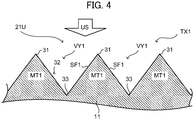
- FIG. 4 is a cross-sectional view of mountains MT1 on the uneven surface of the major surface 21U.
- FIG. 1 is a cross-sectional view of mountains MT2 on the uneven surface of the major surface 21B.
- both the major surfaces 21B and 21U of the crystal substrate 11 has an uneven surface formed by pyramidal mountains MT (MT1/MT2), which have slope faces SF (SF1/SF2), and valleys VY (VY1/VY2).
- MT1/MT2 pyramidal mountains MT
- SF1/SF2 slope faces SF
- VY1/VY2 valleys VY
- An uneven surface is created such that, when the silicon substrate 11 having the (100) plane is anisotropically etched using an alkaline solution, the (111) plane having a slower etching rate will preferentially appear on the surface.
- the mountain MT1 [first mountain MT1] on at least part of the major surface 21U [upside major surface] on the upside US of the crystal substrate 11 has a pointed summit 31 and a slope face SF1 [first slope face SF1] that is smooth from a mountain foot 33 to the summit 31.
- the smooth slope face SF1 herein means a surface, in which the slope face SF1 does not internally have a broken line (see the broken line BL in FIGS. 1 to 3 ); and an example thereof is a slope face SF1 created by performing known alkaline etching on the silicon substrate 11 as described above (hereinafter, an uneven surface created by including the mountain MT1 having the slope face SF1 is referred to as a first texture surface TX1).
- the pointed shape means a shape in which the summit 31 is not spherical but tapered and angular, in which the shape of the summit 31 is understandable as a point in the cross-section CS described later.
- the mountain MT2 [second mountain MT2] on at least part of the major surface 21B [backside major surface] of the backside BS has a pointed summit 31 and a slope face SF2 [second slope face SF2], in which an angle of inclination from the mountain foot 33 to a mountain side 32 differs from an angle of inclination from the mountain side 32 to the summit 31. That is, since the broken line (border line) BL is generated in the mountain side 32 between the summit 31 and the mountain foot 33, the angle of inclination of the slope face SF2 differs between one part (SF231) and the other part (SF233).
- the cross-section CS is used for specifying the shape of the mountain MT on the uneven surface (21B, 21U) in detail; as shown in FIG. 3 , the cross-section CS is a cross-section (cross-sectional direction) CS passing through the summit 31 of the mountain MT (the mountain MT1 is illustrated as an example in FIG. 3 ) and being orthogonal to the mountain foot 33.
- FIG. 1 shows a cross-section CS of the mountain MT2 on the major surface 21B of the backside BS; and FIG. 4 shows a cross-section CS of the mountain MT1 on the major surface 21U of the upside US.
- the slope face SF1 is smooth in the cross-section of the mountain MT1 on the major surface 21U, the entire surface of the slope face SF1 has the same angle of inclination.
- the cross-section CS of the mountain MT2 on the backside 21B is as follows. That is, a minimum angle ⁇ [°] formed by a first imaginary straight line L1 from the mountain foot 33 to the summit 31 and a second imaginary straight line L2 from the mountain foot 33 to the broken line BL [inflection point BL in the cross-section CS] of the mountain side 32 is 1.5 ⁇ 8 (Equation 1).
- the mountain MT2 having such a slope face SF2 occupies 20% or more of the area of the backside 21B.
- the mountain MT2 having the slope face SF2 occupies the entire surface of the backside 21B (hereinafter, an uneven surface generated by including the mountain MT2 having the slope face SF2 is referred to as a second texture surface TX2).
- the reflected light travels in different directions depending on whether the light is incident on the slope face part SF233 to the mountain foot side, or incident on the slope face part SF231 to the summit side.
- the photoelectric conversion efficiency of the solar cell 10 improves.
- the minimum angle ⁇ [°] is measured, for example, by analyzing an image obtained by a scanning electron microscope (SEM) that photographed a cross-section orthogonal to the major surface 21 of the crystal substrate 11 in a range of 10 mm.
- SEM scanning electron microscope
- the first imaginary straight line L1 and the second imaginary straight line L2 were defined by analyzing images of five mountains MT2 confirmed in the images, and a mean value of minimum angles obtained from these images was set to ⁇ [°].
- the minimum angle ⁇ [°] is more preferably 2 ⁇ 5.5, and still more preferably 2.3 ⁇ 2.6.
- the solar cell 10 of a double-side contact type has been described above, in which the p-type semiconductor layer 15 is formed on the side of the major surface 21U on the upside (light reception side) US, and the n-type semiconductor layer 16 is formed on the side of the major surface 21B of the backside (non-light reception side) BS; however, the present invention is not limited thereto.
- the solar cell 10 may be of a back contact type, in which the n-type semiconductor layer 16 and the p-type semiconductor layer 15 are formed on the major surface 21B of the backside BS.
- the mountains MT2 satisfying the above equation (1) are arranged in an area covered with the n-type semiconductor layer 16 (more specifically, an i-type semiconductor layer 14n immediately below the n-type semiconductor layer 16) on the major surface 21B of the crystal substrate 11.
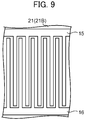
- each of the semiconductor layers 15 and 16 is made into a comb-tooth shape, and the teeth of one comb-tooth shape are arranged between the teeth of the other comb-tooth shape. Therefore, the mountains MT2 having such a slope face SF2 occupy 20% or more of the area of the backside 21B. For example, in the solar cell 10 as shown in FIG. 9 , the mountains MT2 having the slope face SF2 occupy 50% of the area of the backside 21B.
- FIGS. 10A to 10I an example of a method for manufacturing the solar cell 10 of a double-side contact type is described with reference to FIGS. 10A to 10I .
- the crystal substrate 11 having the (100) plane is etched using an alkaline solution.
- This etching is anisotropic etching, in which the (111) plane having a slower etching rate preferentially appears on the surface.
- both the major surfaces 21U and 21B of the crystal substrate 11 change to the first texture surface TX1 [first texture surface forming step].
- alkali components in the etching solution may include a sodium hydroxide, a potassium hydroxide, or an alkali metal such as calcium hydroxide, or a hydroxide of an alkaline earth metal. Among these, a sodium hydroxide or a potassium hydroxide is preferable.
- the alkali component may be a single component or a mixture of two or more components.
- the alkali concentration in the etching solution is preferably between 1% by weight and 20% by weight inclusive, more preferably between 2% by weight and 15% by weight inclusive, and still more preferably between 3% by weight and 10% by weight inclusive.
- IPA isopropyl alcohol
- anisotropic etching IPA (isopropyl alcohol) or the like may be added to an alkaline solution using potassium hydroxide or sodium hydroxide as an etching solution.
- a sacrificial layer 41 is formed of e.g. i-type amorphous silicon on the major surface 21B of the backside BS of the crystal substrate 11.
- the major surface 21B, on which the sacrificial layer 41 is formed, is etched using a mixed solution of ozone dissolved in hydrofluoric acid or the like (described later), whereby obtaining the slope face SF2.
- the i-type semiconductor layer 14p is formed on the major surface 21U of the upside US of the crystal substrate 11, and the p-type semiconductor layer 15 is further formed on the layer 14p.
- a resist film 42 is formed as a protective film on the p-type semiconductor layer 15.
- the crystal substrate 11 having the resist film 42 on the outermost surface of the upside US and having the sacrificial layer 41 on the outermost surface of the backside BS is etched using e.g. a mixed solution of hydrofluoric acid and an oxidizing solution [second texture surface forming step].
- a mixed solution of hydrofluoric acid and an oxidizing solution [second texture surface forming step].
- the sacrificial layer 41 [amorphous silicon layer] and the major surface 21B of the backside BS are etched, and the first texture surface TX1 of the major surface 21B changes to the second texture surface TX2.
- the major surface 21U of the upside US is not etched and remains the first texture surface TX1.
- Etching of an amorphous silicon layer or a crystal substrate (silicon substrate) using a mixed solution of ozone dissolved in hydrofluoric acid proceeds by repeatedly forming an oxide film on a silicon surface using ozone and etching the oxide film using hydrofluoric acid.
- the rate of forming the oxide film using ozone and the rate of etching using hydrofluoric acid are affected by an uneven surface. That is, in the immediate vicinity of the uneven surface of the silicon substrate, the mixed solution more easily migrates in the vicinity of the summits of the uneven surface, and a larger amount of ozone and hydrofluoric acid is likely to be supplied, than in the vicinity of the valleys. Therefore, the etching rate tends to be higher in the vicinity of the summits of the uneven surface than in the vicinity of the valleys.
- An example of such a mixed solution of hydrofluoric acid and an oxidizing solution may include a mixed solution of ozone dissolved in hydrofluoric acid.
- the value XY [weight % 2 ] obtained by multiplying the hydrofluoric acid concentration X [weight %] and the ozone concentration Y [weight %] is preferably between 0.005 and 0.285 inclusive, more preferably between 0.015 and 0.100 inclusive, still more preferably between 0.030 and 0.050 inclusive. This is because the second texture surface TX2 is appropriately formed when the value XY falls within the above-mentioned range.
- the hydrofluoric acid concentration X is preferably between 1.5% by weight and 25% by weight inclusive; even within this range, the hydrofluoric acid concentration X is preferably 5% by weight or more, more preferably 7% by weight or more, and still more preferably 8% by weight or more.
- the ozone concentration Y is not limited in particular, as long as the value XY falls within the above-mentioned preferable range.
- the resist film 42 (see FIG. 10F ) is removed, and the i-type semiconductor layer 14n is formed on the major surface 21B of the crystal substrate 11 which became the second texture surface TX2; and the n-type semiconductor layer 16 is further formed on the layer 14n.
- the transparent electrode layer 17 is formed on the upside US and the backside BS of the crystal substrate 11. Further, as shown in FIG. 10I , a planar metal electrode 18n is formed on the transparent electrode layer 17n of the backside BS of the crystal substrate 11 by e.g. a sputtering method, and a linear metal electrode layer 18p is formed on the transparent electrode layer 17p of the upside US by using a mesh screen (not shown) that has an opening.
- a mesh screen not shown
- the n-type crystal substrate 11 is prepared and subsequently etched using an alkaline solution (see FIG. 11A ), as in the case of the solar cell 10 of a double-side contact type. Through this etching, both the major surfaces 21U and 21B of the crystal substrate 11 change to the first texture surface TX1 [first texture surface forming step].
- the i-type amorphous silicon layer 14 is formed on the major surface 21U of the upside US of the crystal substrate 11; and an anti-reflective layer 43 is further formed on the i-type amorphous silicon layer 14.
- the anti-reflective layer 43 is formed of silicon nitride or silicon oxide, which has a suitable light absorption coefficient and refractive index.
- the i-type semiconductor layer 14 is formed on the major surface 21B of the backside BS of the crystal substrate 11; and the p-type semiconductor layer 15 is further formed on the layer 14.
- the resist film 44 is formed on substantially the entire surface of the anti-reflective layer 43 of the upside US of the crystal substrate 11.
- a resist film (not shown) is formed on part of the p-type semiconductor layer 15; and another part uncovered with the resist film is etched [second texture surface forming step].
- a mixed solution of hydrofluoric acid and an oxidizing solution is used, as in the case of the solar cell 10 of a double-side contact type.
- the p-type semiconductor layer 15, the i-type semiconductor layer 14, and the major surface 21B of the backside BS are etched, and the first texture surface TX1 of the major surface 21B changes to the second texture surface TX2.
- the resist film 44 see FIG. 11C
- the major surface 21U of the upside US is not etched due to the resist film 44 and remains the first texture surface TX1.
- the i-type semiconductor layer 14n is formed on the p-type semiconductor layer 15 and the exposed major surface 21 B; and the n-type semiconductor layer 16 is formed on the layer 14n.
- the i-type semiconductor layer 14n and the n-type semiconductor layer 16 are patterned into a desired shape by, e.g. etching using a resist film (not shown).
- the transparent electrode layer 17 (17p, 17n) is formed on the backside BS of the crystal substrate 11 by a sputtering method using a mask so as to form a separation trench 25 (see FIG. 11F ).
- the separation trench 25 makes it difficult for leakage to occur.
- a linear metal electrode layer 18 (18p, 18n) is formed on the transparent electrode layer 14 by using a mesh screen that has an opening (not shown).
- the mountain MT1 on the uneven surface formed on at least part of the major surface 21U of the light reception side US in the crystal substrate 11 has the pointed summit 31 and the slope face SF1 which is smooth from the mountain foot 33 to the summit 31.
- the mountain MT2 on the uneven surface formed on at least part of the major surface 21B of the non-light reception side BS has the pointed summit 31 and the slope face SF2, in which the angle of inclination from the mountain foot 33 to the mountain side 32 differs from the angle of inclination from the mountain side 32 to the summit 31.
- the minimum angle ⁇ [°] formed by the first imaginary straight line L1 from the mountain foot 33 to the summit 31 and the second imaginary straight line L2 from the mountain foot 33 to the inflection point BL of the mountain side 32 is 1.5 ⁇ 8 (Equation 1); and the mountains MT2 occupy 20% or more of the area of the major surface 21B (the second texture surface TX2 occupies 20% or more of the area of the major surface 21B).
- the solar cell 10 can sufficiently capture light and secure a high photoelectric conversion efficiency. Therefore, the solar cell module modularizing the solar cell 10 has an extremely high power-generation capability.
- the minimum angle ⁇ [°] is more preferably 2 ⁇ 5.5, and still more preferably 2.3 ⁇ 2.6.
- the major surface 21B and the amorphous silicon layer laminated on the major surface 21B are etched using a mixed solution of ozone dissolved in hydrofluoric acid (which may hereinafter be referred to as ozone hydrofluoric acid).
- the resist film 42 (see FIG. 10F ) of the solar cell 10 of a double-side contact type or the resist film 44 ( FIG. 11C ) of the solar cell 10 of a back contact type can hardly be damaged by etching. Therefore, unexpected structural changes are unlikely to occur.
- an etching solution such as ozone hydrofluoric acid, which is less acidic than e.g. hydrofluoric nitric acid
- the amorphous silicon layer serves as a buffer layer against the etching of the crystal substrate 11, whereby completing the second texture surface TX2.
- the synergistic effect by the second texture surface TX2 of the backside BS and the first texture surface TX1 of the upside US enhances the optical confinement effect in the crystal substrate 11.
- the thickness of the amorphous silicon layer may have a distribution.
- the amorphous silicon layer which is composed of the i-type semiconductor layer 14 and the p-type semiconductor layer 15 of the backside 21B of the crystal substrate 11 in the solar cell 10 of a back contact type shown in FIG. 11C
- the amorphous silicon layer may be formed so that the film thickness of the amorphous silicon layer at the summit 31 of the mountain MT2 is smaller than the film thickness of the amorphous silicon layer at the mountain side 32 of the mountain MT2.
- an i-type amorphous silicon thin film is formed by the plasma CVD method
- plasma discharging is performed while introducing hydrogen into the CVD chamber, and a hydrogen plasma treatment (hydrogen plasma etching) is performed on the surface of the i-type amorphous silicon thin film, whereby the i-type semiconductor layer 14 can be formed, in which the film thickness at the summit 31 of the mountain MT2 is smaller than the film thickness at the mountain side 32 of the mountain MT2.
- a hydrogen plasma treatment hydrogen plasma etching
- the crystal substrate 11 is etched in the vicinity of the summit 31 having a smaller film thickness of the amorphous silicon layer, whereby the above-described second texture surface TX2 can be easily formed.
- a hydrogen plasma treatment may be performed while introducing hydrogen and a small amount of silicon-containing gas (e.g. SiH 4 ) into the CVD chamber.
- silicon-containing gas e.g. SiH 4
- the etching by hydrogen plasma and the film formation by CVD using a silicon-containing gas existing in the atmosphere proceed in parallel; however, by adjusting the condition and duration of the hydrogen plasma treatment, the film thickness at the summit 31 of the mountain MT2 can be made smaller than the film thickness at the mountain side 32 of the mountain MT2.
- Such a hydrogen plasma treatment adding a small amount of silicon-containing gas has a smaller rate of change in the film thickness than that of the hydrogen plasma treatment which only uses hydrogen (hydrogen plasma etching); therefore, the film thickness distribution can be more strictly controlled.
- the backside 21B of the crystal substrate 11 corresponding to the amorphous silicon layer which was not etched due to the resist film (other part other than the part where the second texture surface is formed), i.e. the backside 21B of the crystal substrate 11 corresponding to the p-type semiconductor layer 15 and the i-type semiconductor layer 14 corresponding thereto, is the first texture surface having the mountains MT1 and the valleys VY1.
- the film thickness of the amorphous silicon layer at the summit 31 of the mountain MT1 on the backside 21B is smaller than the film thickness of the amorphous silicon layer at the mountain side 32 of the mountain MT1.
- the film thickness of the i-type semiconductor layer 14 at the summit 31 of the mountain MT1 is smaller than the film thickness of the i-type semiconductor layer 14 at the mountain side 32 of the mountain MT1. Still more specifically, the ratio d 2 /d 1 of the film thickness d 2 of the i-type semiconductor layer 14 at the summit 31 of the mountain MT1 to the film thickness d 1 of the i-type semiconductor layer 14 at the mountain side 32 of the mountain MT1 of the backside 21B is smaller than the ratio D 2 /D 1 of the film thickness D 2 of the p-type semiconductor layer 15 at the summit 31 of the mountain MT1 to the film thickness D 1 of the p-type semiconductor layer 15 at the mountain side 32 of the mountain MT1 of the backside 21B.
- the sacrificial layer 41 When the sacrificial layer 41 is formed on the backside 21B of the crystal substrate 11 in the solar cell 10 of a double-side contact type shown in FIG. 10C , the sacrificial layer 41 may be formed so that the film thickness of the sacrificial layer 41 at the summit 31 of the mountain MT2 is smaller than the film thickness of the sacrificial layer 41 at the mountain side 32 of the mountain MT2.
- the crystal substrate 11 is etched in the vicinity of the summit 31 having a smaller film thickness of the sacrificial layer 41, whereby the above-described second texture surface TX2 can be easily formed.
- the value XY [weight % 2 ] obtained by multiplying the hydrofluoric acid concentration X [weight %] and the ozone concentration Y [weight %] is preferably between 0.005 and 0.285 inclusive.
- the value XY [weight % 2 ] is more preferably between 0.015 and 0.1 inclusive, and still more preferably between 0.03 and 0.05 inclusive.
- the hydrofluoric acid concentration X is preferably between 1.5% by weight and 25% by weight inclusive, more preferably between 5% by weight and 25% by weight inclusive, still more preferably between 7% by weight and 25% by weight inclusive, and even more preferably between 8% by weight and 25% by weight inclusive.
- n-type single crystal silicon substrate having a thickness of 200 ⁇ m in the plane orientation of the plane of incidence (100) was used.
- the silicon substrate was immersed in a 2% by weight hydrofluoric acid (HF) aqueous solution for 3 minutes to remove the silicon oxide film from the surface, and then rinsed twice with ultrapure water.
- HF hydrofluoric acid
- the silicon substrate was immersed in a 5 weight %/15 weight % KOH/isopropyl alcohol aqueous solution held at 70°C for 15 minutes. As a result, both the major surfaces of the silicon substrate were etched, and texture (uneven surface) was formed [first texture surface forming step]. Thereafter, the silicon substrate was rinsed twice with ultrapure water.
- a silicon substrate having a first texture surface (first TX surface) on both sides was introduced into a CVD device.
- a sacrificial layer of i-type amorphous silicon having a film thickness of 6 nm was formed on one major surface (major surface which will be the non-light reception side).
- the film-forming conditions for the i-type amorphous silicon film were as follows: the substrate temperature was 150°C, the pressure was 120 Pa, the SiH 4 /H 2 flow rate ratio was 3/10, and the input power density was 0.011 W/cm 2 .
- the film thickness of the thin film was calculated from the film-forming rate obtained by measuring the film thickness of the thin film formed on the glass substrate under the same conditions by spectroscopic ellipsometry (trade name: M2000; manufactured by J. A. Woollam Corporation).
- an i-type semiconductor layer of i-type amorphous silicon having a film thickness of 6 nm was formed on the other major surface (major surface which will be the light reception side).
- the film-forming conditions for the i-type amorphous silicon film were as follows: the substrate temperature was 150°C, the pressure was 120 Pa, the SiH 4 /H 2 flow rate ratio was 3/10, and the input power density was 0.011 W/cm 2 .
- a p-type semiconductor layer of p-type amorphous silicon having a conductivity type opposite to the conductivity type of the n-type single crystal silicon substrate and having a film thickness of 7 nm was formed on the i-type amorphous silicon layer.
- the film-forming conditions for the p-type amorphous silicon were as follows: the substrate temperature was 150°C, the pressure was 60 Pa, the SiH 4 /B 2 H 6 flow rate ratio was 1/3, and the input power density was 0.01 W/cm 2 .
- the B 2 H 6 gas flow rate herein is a flow rate of a diluent gas diluted with H 2 to a B 2 H 6 density of 5000 ppm.
- a resist film was formed as a protective film on the p-type semiconductor layer.
- the silicon substrate having the resist film on the outermost surface on one side and having the sacrificial layer on the outermost surface on the other side was immersed in a mixed solution (etching solution) of 1 weight % HF aqueous solution and 20 ppm ozone for 8 minutes.
- This etching [second texture surface forming step] resulted in etching the sacrificial layer and the major surface immediately thereunder; and the first texture surface of the major surface changed to the second texture surface (second TX surface).
- the major surface covered with the resist film was not etched and remained the first texture surface. After this etching, the resist film was removed.
- the silicon substrate before and after this etching was used to photograph a cross-section orthogonal to the major surface of the silicon substrate in a range of 10 mm under a scanning electron microscope (SEM), and the texture surface was measured by analyzing the images.
- the first imaginary straight line and the second imaginary straight line were determined by analyzing images of mountains at five locations of the second texture surface confirmed in the images, and a mean value obtained therefrom was set to ⁇ [°].
- an i-type semiconductor layer of i-type amorphous silicon was formed on the major surface, on which the second texture surface was formed.
- the film thickness and the film-forming conditions were the same as those of the i-type semiconductor layer immediately below the p-type semiconductor layer.
- n-type semiconductor layer of n-type amorphous silicon having a film thickness of 4 nm was formed on the i-type amorphous silicon layer.
- the film-forming conditions for the n-type amorphous silicon were as follows: the substrate temperature was 150°C, the pressure was 60 Pa, the SiH 4 /PH 3 flow rate ratio was 1/2, and the input power density was 0.01 W/cm 2 .
- the PH 3 gas flow rate herein is a flow rate of a diluent gas diluted with H 2 to a PH 3 density of 5000 ppm.
- ITO indium tin oxide
- This film formation was performed as follows: indium oxide was used as a target, the substrate temperature was room temperature, the pressure was 0.2 Pa in an argon atmosphere, and the power density of 0.5 W/cm 2 was applied.
- a silver-electrode layer (planar electrode) having a film thickness of 500 nm was formed on the transparent electrode layer on the n-type semiconductor layer by way of a sputtering method.
- the silicon substrate was removed from the outer peripheral edge into a width of 0.5 mm by way of a laser beam machine, and was used as a heterojunction solar cell of a double-side contact type of Example 1.
- the solar cells of Examples 2 to 9 were produced in the same manner as in Example 1 except that the ozone concentration and the hydrofluoric acid concentration were changed as shown in Table 1 below, in the etching using a mixed solution of ozone dissolved in hydrofluoric acid in Example 1 (hereinafter referred to as the second texture surface forming step).
- the solar cell of Example 10 was produced in the same manner as in Example 1 except that only 20% of the area of the major surface of the silicon substrate was the second texture surface, in the second texture surface forming step.
- Comparative Example 1 is the solar cell having the first texture surface on both major surfaces of the silicon substrate.
- the solar cell of Comparative Example 2 was produced in the same manner as in Example 1 except that only 10% of the area of the major surface of the silicon substrate was the second texture surface, in the second texture surface forming step.
- the solar cell of Comparative Example 3 was produced in the same manner as in Example 1 except that the second texture surface was formed on both major surfaces of the silicon substrate without using a resist film, and thereafter, the i-type semiconductor layer was further formed on the major surface which will be the light reception side, and the p-type semiconductor layer was further formed on the layer, in the second texture surface forming step.
- the solar cells of Comparative Examples 4 to 6 were produced in the same manner as in Example 1 except that the ozone concentration and the hydrofluoric acid concentration were changed as shown in Table 1 below, in the etching using the mixed solution of ozone dissolved in hydrofluoric acid as described above.
- the production was performed in the same manner as in Example 1 except that, instead of the etching using a mixed solution of ozone dissolved in hydrofluoric acid as described above, immersion was carried out for 1 minute using a solution, in which a 48 weight % HF aqueous solution and concentrated nitric acid were mixed at a ratio of 1:80.
- Example 11 is a heterojunction solar cell of a back contact type. In the same manner as in Example 1, texture was formed on both major surfaces of the silicon substrate [first texture surface forming step].
- the silicon substrate having the first texture surface on both sides was introduced into a CVD device. Then, an i-type semiconductor layer of i-type amorphous silicon having a film thickness of 5 nm was formed on the major surface which will be the light reception side.
- the film-forming conditions for the i-type amorphous silicon film were as follows: the substrate temperature was 150°C, the pressure was 120 Pa, the SiH 4 /H 2 flow rate ratio was 3/10, and the input power density was 0.011 W/cm 2 .
- an anti-reflective layer having a film thickness of 100 nm was formed on the i-type amorphous silicon layer.
- the film-forming conditions for the anti-reflective layer were as follows: the substrate temperature was 150°C, the pressure was 80 Pa, the NH 3 /SiH 4 /H 2 flow rate ratio was 1/1/40, and the input power density was 0.2 W/cm 2 .
- an i-type semiconductor layer of i-type amorphous silicon having a film thickness of 6 nm was formed on the major surface which will be the non-light reception side.
- the film-forming conditions for the i-type amorphous silicon film were as follows: the substrate temperature was 150°C, the pressure was 120 Pa, the SiH 4 /H 2 flow rate ratio was 3/10, and the input power density was 0.011 W/cm 2 .
- n-type semiconductor layer of n-type amorphous silicon having a film thickness of 7 nm was formed on the i-type amorphous silicon layer.
- the film-forming conditions for the p-type amorphous silicon were as follows: the substrate temperature was 150°C, the pressure was 60 Pa, the SiH 4 /B 2 H 6 flow rate ratio was 1/3, and the input power density was 0.01 W/cm 2 .
- a protective film As a protective film, a resist film was formed on substantially the entire surface of the anti-reflective layer on the upside of the crystal substrate, and a resist film was pattern-printed on the p-type semiconductor layer. Then, the silicon substrate covered with the resist film (resist pattern) was immersed in a mixed solution (etching solution) of 1 weight % HF aqueous solution and 20 ppm ozone for 15 minutes.
- etching solution 1 weight % HF aqueous solution and 20 ppm ozone for 15 minutes.
- This etching [second texture surface forming step] resulted in etching the major surface of the p-type semiconductor layer, the i-type semiconductor layer and the non-light reception side which are uncovered with the resist film; and the first texture surface of the major surface changed to the second texture surface.
- the major surface of the light reception side was not etched due to the resist film and remained the first texture surface.
- the ratio of the opening area to the non-opening area in the resist pattern was 1:1. Therefore, the area ratio of the remaining p-type semiconductor layer to the n-type semiconductor layer described later is 1:1.
- an i-type semiconductor layer of i-type amorphous silicon having a film thickness of 5 nm was formed on the p-type semiconductor layer and the major surface exposed.
- the film thickness and the film-forming conditions were the same as those for the i-type semiconductor layer immediately below the p-type semiconductor layer.
- n-type semiconductor layer of n-type amorphous silicon having a film thickness of 4 nm was formed on the i-type amorphous silicon layer.
- the film-forming conditions for the n-type amorphous silicon were as follows: the substrate temperature was 150°C, the pressure was 60 Pa, the SiH 4 /PH 3 flow rate ratio was 1/2, and the input power density was 0.01 W/cm 2 .
- part of the n-type semiconductor layer on the p-type semiconductor layer was patterned by, for example, etching using a resist film.
- a transparent electrode layer of indium tin oxide (ITO; refractive index of 1.9) having a film thickness of 100 nm was formed on the p-type semiconductor layer and the n-type semiconductor layer thus patterned, by way of a sputtering method using a mask so as to form a separation trench.
- This film formation was performed as follows: indium oxide was used as a target, the substrate temperature was room temperature, the pressure was 0.2 Pa in an argon atmosphere, and the power density of 0.5 W/cm 2 was applied.
- the silicon substrate was removed from the outer peripheral edge into a width of 0.5 mm by way of a laser beam machine, and was used as a heterojunction solar cell of a back contact type of Example 12.
- the production was performed in the same manner as in Example 11 except that, instead of the etching using a mixed solution of ozone dissolved in hydrofluoric acid as described above, immersion was carried out for 1 minute using a solution, in which a 48 weight % HF aqueous solution and concentrated nitric acid were mixed at a ratio of 1:80.
- the solar cell of Example 12 was produced in the same manner as in Example 11 except that a hydrogen plasma treatment using hydrogen H 2 and silicon-containing gas SiH 4 was performed on the major surface, which will be the non-light reception side, after forming the i-type semiconductor layer and before forming the p-type semiconductor layer in Example 11.
- the crystal substrate 11 was etched in the vicinity of the summits 31 having a smaller film thickness of the amorphous silicon layer; and the second texture surface TX2 described above was formed.
- the production was performed in the same manner as in Example 12 except that, instead of the etching using a mixed solution of ozone dissolved in hydrofluoric acid as described above, immersion was carried out for 1 minute using a solution, in which a 48 weight % HF aqueous solution and concentrated nitric acid were mixed at a ratio of 1:80.
- Table 1 shows a measurement result such as conditions for manufacturing a heterojunction solar cell (hydrofluoric acid concentration [X], ozone concentration [Y], hydrofluoric acid concentration ⁇ ozone concentration [XY]) and the minimum angle ⁇ [°] as well as solar cell characteristics (open-circuit voltage (Voc), short-circuit current density (Isc), fill factor (FF), conversion efficiency (Eff)) in the Examples and Comparative Examples described above.
- the solar cell characteristics (Voc, Isc, FF, Eff) of Examples 1 to 10 and Comparative Examples 2 to 7 are relative values in relation to the solar cell characteristics (Voc, Isc, FF, Eff) of Comparative Example 1.
- the solar cell characteristics (Voc, Isc, FF, Eff) of Example 11 are relative values in relation to the solar cell characteristics (Voc, Isc, FF, Eff) of Comparative Example 8; and the solar cell characteristics (Voc, Isc, FF, Eff) of Example 12 are relative values in relation to the solar cell characteristics (Voc, Isc, FF, Eff) of Comparative Example 9.
- the minimum angle ⁇ [°] is preferably 1.5 ⁇ 8, more preferably 2 ⁇ 5.5, and still more preferably 2.3 ⁇ 2.6.
- the value XY is preferably between 0.005 and 0.285 inclusive, more preferably between 0.015 and 0.1 inclusive, and still more preferably between 0.03 and 0.05 inclusive.
- Example 1 to 8 the open-circuit voltage Voc was also improved as compared with Comparative Example 1. This is considered to be because the defects in the amorphous silicon layer formed on the second texture surface were reduced.
- the conversion efficiency was not sufficiently improved in Comparative Example 2, in which the second texture surface was only formed in 10% of the area of the major surface of the non-light reception side.
- the conversion efficiency was sufficiently improved in Example 10, in which the second texture surface was formed in 20% of the area of the major surface of the non-light reception side, or in Example 1 to 9, in which the entirety (100%) of the major surface of the non-light reception side was the second texture surface.
- Example 1 Comparative Example 3 which share the same minimum angle ⁇ [°]
- the short-circuit current in Comparative Example 3 was lower than that in Example 1. This is considered to be because, when the second texture surface was formed not only on the non-light reception side but also on the major surface of the light reception side, the reflectance increasing effect caused by the major surface of the light reception side exceeded the optical confinement effect caused by the major surface of the non-light reception side.
- Example 11 and Comparative Example 8 As well as comparison between Example 12 and Comparative Example 9, which are the solar cell of a back contact type, it was found that the conversion efficiency was improved when the non-light reception side had the second texture surface, and the light reception side had the first texture surface in the crystal substrate. That is, regardless of a double-side contact type or a back contact type, the conversion efficiency can be enhanced when the solar cell includes a crystal substrate having the second texture surface on the non-light reception side and the first texture surface on the light reception side.
Landscapes
- Photovoltaic Devices (AREA)
- Life Sciences & Earth Sciences (AREA)
- Engineering & Computer Science (AREA)
- Sustainable Energy (AREA)
Abstract
Description
- The present invention relates to a solar cell, a solar cell module, and a solar cell manufacturing method.
- Although many types of solar cells are available, a solar cell using a single crystal silicon substrate is recently becoming mainstream. In such a solar cell, a structure referred to as texture, which is made uneven by arranging pyramidal mountains, is formed on a major surface of a single crystal silicon substrate. This is because the presence of such texture can suppress light reflection from a major surface that receives light, and can facilitate confining incident light in the solar cell.
- Various developments have been made with respect to a structure of such texture; for example, in
Patent Document 1, a summit of a pyramidal mountain is rounded, whereby the summit becomes less likely to chip, preventing carrier recombination due to chipping. - Patent Document 1:
PCT International Publication No. WO 2014/083804 - However, in a single crystal silicon substrate, the presence of a rounded shape on a light reception side is conversely likely to reflect the received light, which may deteriorate the efficiency of the solar cell.
- The present invention has been made to solve the above problems. It is an object of the present invention to provide a solar cell or the like having an enhanced conversion efficiency.
- As for a solar cell including a crystal substrate according to the present invention, among both major surfaces of the crystal substrate, at least part of a frontside major surface, which is the major surface that receives light, is an uneven surface formed by a first mountain and a first valley. The first mountain has a pointed summit and a first slope face that is smooth from a mountain foot to the summit.
- At least part of a backside major surface, which is a surface opposite to the frontside major surface, is an uneven surface formed by a second mountain and a second valley. The second mountain has a pointed summit and a second slope face, in which an angle of inclination from a mountain foot to a mountain side differs from an angle of inclination from the mountain side to the summit.
- The second slope face is configured as follows. That is, in a cross-section passing through the summit and being perpendicular to the mountain foot, the minimum angle θ[°] formed by a first imaginary straight line from the mountain foot to the summit and a second imaginary straight line from the mountain foot to a inflection point at the mountain side is 1.5≤θ≤8. In addition, the second mountain occupies 20% or more of an area of the backside major surface.
- Further, as for a method for manufacturing a solar cell including a crystal substrate according to the present invention, among both major surfaces of the crystal substrate, when etching a side of a backside major surface, which is a surface opposite to a frontside major surface that receives light, a mixed solution of ozone dissolved in hydrofluoric acid is used for the backside major surface and an amorphous silicon layer to be laminated thereon. In this mixed solution, a value XY [weight %] obtained by multiplying a hydrofluoric acid concentration X [weight %] and an ozone concentration Y [weight %] is between 0.005 and 0.285 inclusive.
- According to the present invention, a solar cell or the like having an enhanced conversion efficiency is provided.
-
-
FIG. 1 is a cross-sectional view of mountains on an uneven surface of a major surface on a backside; -
FIG. 2 is an enlarged perspective view of part of a major surface of a crystal substrate on a backside of a solar cell; -
FIG. 3 is an explanatory view for explaining a cross-section; -
FIG. 4 is a cross-sectional view of the mountains on the uneven surface of the major surface on the frontside; -
FIG. 5 is an enlarged perspective view showing part of the major surface of the crystal substrate on the frontside of the solar cell; -
FIG. 6 is a cross-sectional view of a solar cell of a double-side type; -
FIG. 7 is an explanatory view for explaining the progress of light; -
FIG. 8 is a cross-sectional view of a solar cell of a back contact type; -
FIG. 9 is a schematic plan view of the solar cell of a back contact type; -
FIG. 10A is an explanatory view showing a process of manufacturing a solar cell of a double-side contact type; -
FIG. 10B is an explanatory view showing a process of manufacturing the solar cell of a double-side contact type; -
FIG. 10C is an explanatory view showing a process of manufacturing the solar cell of a double-side contact type; -
FIG. 10D is an explanatory view showing a process of manufacturing the solar cell of a double-side contact type; -
FIG. 10E is an explanatory view showing a process of manufacturing the solar cell of a double-side contact type; -
FIG. 10F is an explanatory view showing a process of manufacturing the solar cell of a double-side contact type; -
FIG. 10G is an explanatory view showing a process of manufacturing the solar cell of a double-side contact type; -
FIG. 10H is an explanatory view showing a process of manufacturing the solar cell of a double-side contact type; -
FIG. 10I is an explanatory view showing a process of manufacturing the solar cell of a double-side contact type; -
FIG. 11A is an explanatory view showing a process of manufacturing the solar cell of a back contact type; -
FIG. 11B is an explanatory view showing a process of manufacturing the solar cell of a back contact type; -
FIG. 11C is an explanatory view showing a process of manufacturing the solar cell of a back contact type; -
FIG. 11D is an explanatory view showing a process of manufacturing the solar cell of a back contact type; -
FIG. 11E is an explanatory view showing a process of manufacturing the solar cell of a back contact type; -
FIG. 11F is an explanatory view showing a process of manufacturing the solar cell of a back contact type; -
FIG. 12 is a graph of a minimum angle θ [°] and a conversion efficiency [%] in Examples 1 to 9 and Comparative Examples 4 to 6; and -
FIG. 13 is a graph of a value XY [weight %2] obtained by multiplying a hydrofluoric acid concentration X [weight %] and an ozone concentration Y [weight %], as well as a conversion efficiency [%], in Examples 1 to 9 and Comparative Examples 4 to 6. - An embodiment of the present invention will be described below; however, the present invention is not limited thereto. For the sake of convenience, hatching, member reference numbers, etc. may be omitted; however, in such cases, other drawings shall be referred to. Dimensions of various members in the drawings are adjusted for the sake of visibility.
-
FIG. 6 shows asolar cell 10 using a silicon-made crystal substrate (crystal silicon substrate) 11. Asolar cell 10 has two major surfaces, in which a side of amajor surface 21U [upside major surface (frontside major surface)] being one side of thecrystal substrate 11 is referred to as an upside (frontside) US, and a side of amajor surface 21B [backside major surface] being the other side of thecrystal substrate 11 is referred to as a backside BS. For the sake of convenience, the upside US will be described as a side (light reception side US) which is caused to more actively receive light than the backside BS; and the backside BS will be described as a non-light reception side BS which is caused not to actively receive light. Thesolar cell 10 will be described below by an example of a so-called heterojunction crystal silicon solar cell (hereinafter, heterojunction solar cell); however, the present invention is not limited thereto. - The
solar cell 10 includes acrystal substrate 11, an intrinsic (i-type)semiconductor layer 14, a p-type semiconductor layer 15, an n-type semiconductor layer 16, atransparent electrode layer 17, and ametal electrode layer 18. - In the following description, silicon is given as an example of the material of the semiconductor layer; however, the present invention is not limited thereto. For the sake of convenience, the reference numbers of members, which are individually associated with the p-
type semiconductor layer 15 or the n-type semiconductor layer 16, may be assigned with the suffix "p"/"n". Since the conductivity types are different such as p-type or n-type, one conductivity type may be referred to as a "first conductivity type" and the other conductivity type may be referred to as a "second conductivity type" in some cases. - The
crystal substrate 11 may be single crystal or polycrystal. Hereinafter, a single crystal silicon substrate will be described as an example. The conductivity type of thecrystal substrate 11 may be either a p-type or an n-type; however, in the following description, an n-type [first conductivity type crystal substrate] supposedly having a long carrier lifetime will be described as an example. - From the viewpoint of confining the received light, the two major surfaces 21 (21U, 21B) of the
crystal substrate 11 are an uneven surface formed by mountains MT and valleys VY. This will be described later in detail. - The intrinsic (i-type) semiconductor layer 14 (14p, 14n) covers the
major surface 21 of thecrystal substrate 11, thereby performing surface passivation while suppressing impurities from diffusing into thecrystal substrate 11. An example of the material for the i-type semiconductor layer 14 may include amorphous silicon or microcrystal silicon (mixture of amorphous silicon and crystal silicon), among which the amorphous silicon formed of silicon and hydrogen is preferable. The i-type semiconductor layer 14 preferably has a thickness to an extent that may not adversely affect the power generation characteristics. - The p-type semiconductor layer [second conductivity type semiconductor layer] 15 is a silicon layer doped with a p-type dopant (such as boron), and is formed on the
intrinsic semiconductor layer 14p of the upside US inFIG. 6 . From the viewpoint of suppressing impurities or reducing series resistance, the p-type semiconductor layer 15 is preferably formed of amorphous silicon. - Examples thereof may include a p-type hydrogenated amorphous silicon layer, a p-type amorphous silicon carbide layer, or a p-type amorphous silicon oxide layer. The p-type amorphous silicon carbide layer and the p-type amorphous silicon oxide layer, which are wide-gap low refractive index layers, are preferable since optical loss can be reduced.
- The n-type semiconductor layer [first conductivity type semiconductor layer] 16 is a silicon layer doped with an n-type dopant (such as phosphorus), and is formed on the
intrinsic semiconductor layer 14n on the backside BS inFIG. 6 . Like the p-type semiconductor layer 15, the n-type semiconductor layer 16 is also preferably formed of an amorphous silicon layer. - Meanwhile, an example of a film-forming method for a silicon-based thin film such as the i-
type semiconductor layer 14, the p-type semiconductor layer 15 and the n-type semiconductor layer 16 may include a plasma CVD method. As the conditions for forming the silicon-based thin film by the plasma-CVD method, the substrate temperature is preferably between 100°C and 300°C inclusive, the pressure is preferably between 20 Pa and 2600 Pa inclusive, and the highfrequency power density is preferably between 0.004 W/cm2 and 0.8 W/cm2 inclusive. - As the source gas, a silicon-containing gas such as SiH4 or Si2H6, or a mixed gas of a silicon-based gas and H2 is preferably used. As the dopant gas, B2H6 or the like is preferably used for forming the p-
type semiconductor layer 15, and PH3 or the like is preferably used for forming the n-type semiconductor layer 16. Since the amount of impurities such as B or P added may be very small, a mixed gas of a dopant gas diluted with a source gas may be used. - In order to adjust the energy gap of the p-
type semiconductor layer 15 or the n-type semiconductor layer 16, a gas containing different elements such as CH4, CO2, NH3 or GeH4 may be added, and the p-type semiconductor layer 15 or the n-type semiconductor layer 16 may be alloyed. - A laminate formed of the
crystal substrate 11, the i-type semiconductor layer 14, the p-type semiconductor layer 15 and the n-type semiconductor layer 16 as described above is referred to as a photoelectric converter. Therefore, in thesolar cell 10 as shown inFIG. 6 , the p-type semiconductor layer 15 / the i-type semiconductor layer 14p / the n-type crystal substrate 11 / the i-type semiconductor layer 14n / and the n-type semiconductor layer 16 are laminated in this order from the upside US to the backside BS. - The transparent electrode layer 17 (17p, 17n) is formed of a conductive oxide, which is translucent to an extent that transmits the light received. Such
transparent electrode layer 17 is formed so as to cover the p-type semiconductor layer 15 or the n-type semiconductor layer 16, thereby being electrically connected to the semiconductor layers 15/16. Thus, thetransparent electrode layer 17 functions as a transport layer for guiding carriers generated in the p-type semiconductor layer 15 or the n-type semiconductor layer 16. AlthoughFIG. 6 shows an example of the singletransparent electrode layer 17, the present invention is not limited thereto, and a multilayeredtransparent electrode layer 17 may be used. - The content of the conductive oxide in the
transparent electrode layer 17 is greater than 50% by weight (such a ratio is described as a principal component). From the viewpoint of conductivity, the content of the conductive oxide is preferably 70% or more by weight, and more preferably 90% or more by weight. - Examples of the conductive oxide may include a material such as zinc oxide, indium oxide or tin oxide, alone or in combination. From the viewpoint of conductivity, optical characteristics, or long-term reliability, an indium-based oxide containing indium oxide is preferable, and among these, indium tin oxide (ITO) as a principal component is more preferable.
- A doping agent may be added to the
transparent electrode layer 17. For example, when zinc oxide is used as thetransparent electrode layer 17, aluminum, gallium, boron, silicon, carbon, or the like may be used as the doping agent. When indium oxide is used as thetransparent electrode layer 17, zinc, tin, titanium, tungsten, molybdenum, silicon, or the like can be used as the doping agent. When tin oxide is used as thetransparent electrode layer 17, fluorine or the like may be used as the doping agent. - The doping agent may be added to both or only one of the
transparent electrode layer 17p covering the p-type semiconductor layer 15 and thetransparent electrode layer 17n covering the n-type semiconductor layer 16; however, it is preferable that the doping agent is added to thetransparent electrode layer 17p of the light reception side US, since the resistance of thetransparent electrode layer 17p itself is lowered, and the resistance loss between thetransparent electrode layer 17p and themetal electrode layer 18p is suppressed. - From the viewpoint of translucency, conductivity, or light reflection reduction, the thickness of the
transparent electrode layer 17 is preferably between 10 nm and 140 nm inclusive. When the film thickness is 10 nm or more, thetransparent electrode layer 17 has sufficient conductivity to transport carriers to themetal electrode layer 18; and when the film thickness is 140 nm or less, light absorbed by thetransparent electrode layer 17 due to thickness does not excessively increase, thereby suppressing decrease in the photoelectric conversion efficiency. That is, if the thickness of thetransparent electrode layer 17 is within the above-mentioned range, increase in carrier density is suppressed even inside thetransparent electrode layer 17, and decrease in photoelectric conversion efficiency due to decrease in transmittance in the infrared region is also suppressed. - The film-forming method for the
transparent electrode layer 17 is not limited in particular; however, a physical vapor deposition (PVD) method such as a sputtering method, a chemical vapor deposition (MOCVD) method using a reaction of an organometallic compound with oxygen or water, or the like can be used. In any of the film-forming methods, energy from heat or plasma discharge may be used. - The temperature for forming the transparent electrode layer 17 (substrate temperature) is appropriately set. For example, when amorphous silicon is used for the silicon-based thin film, the substrate temperature is preferably 200°C or less. This suppresses desorption of hydrogen from amorphous silicon, or suppresses generation of dangling bonds to silicon atoms due to desorption, and consequently improves the conversion efficiency of the solar cell.
- The metal electrode layer 18 (18p, 18n) is formed of a conductive metal. The
metal electrode layer 18 is formed so as to cover thetransparent electrode layer 17, thereby being electrically connected to thetransparent electrode layer 17. As a result, themetal electrode layer 18 further transports carriers transported from thetransparent electrode layer 17. Therefore, themetal electrode layer 18 may be referred to as a collecting electrode. - As the material for the
metal electrode layer 18, it is preferable to use a material having a high reflectance in the near-infrared to infrared region and having a high conductivity or chemical stability. Examples of the material satisfying such characteristics include silver or aluminum. - Examples of the film-forming method for the
metal electrode layer 18 may include, without limitation in particular, a physical vapor deposition method such as a sputtering method or a vacuum evaporation method, a printing method such as screen printing, an electrolytic plating method using a screen-printed metal as a seed, or the like. - In practical use, the
solar cell 10 as described above is modularized. Modularization of thesolar cell 10 is accomplished, for example, such that themetal electrodes 18 of the plurality ofsolar cells 10 are arranged in a matrix, electrically connected to each other via conductive tab wires, and sealed between a pair of transparent substrates. - Here, surface shapes of the upside (light reception side) US and the backside (non-light reception side) BS of the
solar cell 10 will be described with reference toFIG. 6 as well asFIGS. 1 to 5 . -
FIG. 5 is an enlarged perspective view showing part of themajor surface 21U of thecrystal substrate 11 on the upside US of thesolar cell 10.FIG. 2 is an enlarged perspective view showing part of themajor surface 21B of thecrystal substrate 11 on the backside BS of thesolar cell 10.FIG. 3 is an explanatory view for explaining a cross-section CS described later.FIG. 4 is a cross-sectional view of mountains MT1 on the uneven surface of themajor surface 21U.FIG. 1 is a cross-sectional view of mountains MT2 on the uneven surface of themajor surface 21B. - As shown in
FIGS. 6 ,5 and2 , at least part of both themajor surfaces crystal substrate 11 has an uneven surface formed by pyramidal mountains MT (MT1/MT2), which have slope faces SF (SF1/SF2), and valleys VY (VY1/VY2). An uneven surface is created such that, when thesilicon substrate 11 having the (100) plane is anisotropically etched using an alkaline solution, the (111) plane having a slower etching rate will preferentially appear on the surface. - As shown in
FIGS. 5 and4 , the mountain MT1 [first mountain MT1] on at least part of themajor surface 21U [upside major surface] on the upside US of thecrystal substrate 11 has a pointedsummit 31 and a slope face SF1 [first slope face SF1] that is smooth from amountain foot 33 to thesummit 31. - The smooth slope face SF1 herein means a surface, in which the slope face SF1 does not internally have a broken line (see the broken line BL in
FIGS. 1 to 3 ); and an example thereof is a slope face SF1 created by performing known alkaline etching on thesilicon substrate 11 as described above (hereinafter, an uneven surface created by including the mountain MT1 having the slope face SF1 is referred to as a first texture surface TX1). The pointed shape means a shape in which thesummit 31 is not spherical but tapered and angular, in which the shape of thesummit 31 is understandable as a point in the cross-section CS described later. - On the other hand, as shown in
FIG. 2 , the mountain MT2 [second mountain MT2] on at least part of themajor surface 21B [backside major surface] of the backside BS has a pointedsummit 31 and a slope face SF2 [second slope face SF2], in which an angle of inclination from themountain foot 33 to amountain side 32 differs from an angle of inclination from themountain side 32 to thesummit 31. That is, since the broken line (border line) BL is generated in themountain side 32 between thesummit 31 and themountain foot 33, the angle of inclination of the slope face SF2 differs between one part (SF231) and the other part (SF233). - The cross-section CS is used for specifying the shape of the mountain MT on the uneven surface (21B, 21U) in detail; as shown in
FIG. 3 , the cross-section CS is a cross-section (cross-sectional direction) CS passing through thesummit 31 of the mountain MT (the mountain MT1 is illustrated as an example inFIG. 3 ) and being orthogonal to themountain foot 33. -
FIG. 1 shows a cross-section CS of the mountain MT2 on themajor surface 21B of the backside BS; andFIG. 4 shows a cross-section CS of the mountain MT1 on themajor surface 21U of the upside US. As shown inFIG. 4 , since the slope face SF1 is smooth in the cross-section of the mountain MT1 on themajor surface 21U, the entire surface of the slope face SF1 has the same angle of inclination. - On the other hand, as shown in
FIG. 1 , the cross-section CS of the mountain MT2 on thebackside 21B is as follows. That is, a minimum angle θ[°] formed by a first imaginary straight line L1 from themountain foot 33 to thesummit 31 and a second imaginary straight line L2 from themountain foot 33 to the broken line BL [inflection point BL in the cross-section CS] of themountain side 32 is 1.5≤θ≤8 (Equation 1). - The mountain MT2 having such a slope face SF2 occupies 20% or more of the area of the
backside 21B. For example, in the case of thesolar cell 10 as shown inFIG. 6 , the mountain MT2 having the slope face SF2 occupies the entire surface of thebackside 21B (hereinafter, an uneven surface generated by including the mountain MT2 having the slope face SF2 is referred to as a second texture surface TX2). - With this structure, as shown in the explanatory view for explaining light beams in
FIG. 7 (arrows representing light), on themajor surface 21U on the light reception side US, for example, when external light is reflected by the slope face SF1, the reflected light is likely to travel towards themountain foot 33 due to the single smooth surface. Therefore, a large amount of light is likely to enter thecrystal substrate 11. - On the
major surface 21B of the non-light reception side BS, for example, when light having entered thecrystal substrate 11 is reflected by the slope face SF2, the reflected light travels in different directions depending on whether the light is incident on the slope face part SF233 to the mountain foot side, or incident on the slope face part SF231 to the summit side. - For example, when light traveling from the same direction reaches the slope face part SF233 and the slope face part SF231, if the light reflected by the slope face part SF233 is finally transmitted to the outside, the light reflected by the slope face part SF231, which is a different reflective surface, travels in a direction different from the light having been transmitted to the outside and is unlikely to be transmitted to the outside. In other words, an increased variety of light travels inside the
crystal substrate 11. Therefore, a larger amount of light is likely to enter thecrystal substrate 11. Therefore, the photoelectric conversion efficiency of thesolar cell 10 improves. - The minimum angle θ[°] is measured, for example, by analyzing an image obtained by a scanning electron microscope (SEM) that photographed a cross-section orthogonal to the
major surface 21 of thecrystal substrate 11 in a range of 10 mm. In this case, the first imaginary straight line L1 and the second imaginary straight line L2 were defined by analyzing images of five mountains MT2 confirmed in the images, and a mean value of minimum angles obtained from these images was set to θ[°]. - The minimum angle θ[°] is more preferably 2≤θ≤5.5, and still more preferably 2.3≤θ≤2.6.
- The
solar cell 10 of a double-side contact type has been described above, in which the p-type semiconductor layer 15 is formed on the side of themajor surface 21U on the upside (light reception side) US, and the n-type semiconductor layer 16 is formed on the side of themajor surface 21B of the backside (non-light reception side) BS; however, the present invention is not limited thereto. - For example, as shown in the cross-sectional view of
FIG. 8 , thesolar cell 10 may be of a back contact type, in which the n-type semiconductor layer 16 and the p-type semiconductor layer 15 are formed on themajor surface 21B of the backside BS. - In the
solar cell 10 of such a back contact type, the mountains MT2 satisfying the above equation (1) are arranged in an area covered with the n-type semiconductor layer 16 (more specifically, an i-type semiconductor layer 14n immediately below the n-type semiconductor layer 16) on themajor surface 21B of thecrystal substrate 11. - As shown in the schematic plan view of
FIG. 9 , each of the semiconductor layers 15 and 16 is made into a comb-tooth shape, and the teeth of one comb-tooth shape are arranged between the teeth of the other comb-tooth shape. Therefore, the mountains MT2 having such a slope face SF2 occupy 20% or more of the area of thebackside 21B. For example, in thesolar cell 10 as shown inFIG. 9 , the mountains MT2 having the slope face SF2 occupy 50% of the area of thebackside 21B. - Here, an example of a method for manufacturing the
solar cell 10 of a double-side contact type is described with reference toFIGS. 10A to 10I . First, an n-type crystal substrate 11 as shown inFIG. 10A is prepared. - Thereafter, as shown in
FIG. 10B , thecrystal substrate 11 having the (100) plane is etched using an alkaline solution. This etching is anisotropic etching, in which the (111) plane having a slower etching rate preferentially appears on the surface. As a result, both themajor surfaces crystal substrate 11 change to the first texture surface TX1 [first texture surface forming step]. - Examples of alkali components in the etching solution may include a sodium hydroxide, a potassium hydroxide, or an alkali metal such as calcium hydroxide, or a hydroxide of an alkaline earth metal. Among these, a sodium hydroxide or a potassium hydroxide is preferable. The alkali component may be a single component or a mixture of two or more components.
- The alkali concentration in the etching solution is preferably between 1% by weight and 20% by weight inclusive, more preferably between 2% by weight and 15% by weight inclusive, and still more preferably between 3% by weight and 10% by weight inclusive. In anisotropic etching, IPA (isopropyl alcohol) or the like may be added to an alkaline solution using potassium hydroxide or sodium hydroxide as an etching solution.
- Next, as shown in
FIG. 10C , asacrificial layer 41 is formed of e.g. i-type amorphous silicon on themajor surface 21B of the backside BS of thecrystal substrate 11. Themajor surface 21B, on which thesacrificial layer 41 is formed, is etched using a mixed solution of ozone dissolved in hydrofluoric acid or the like (described later), whereby obtaining the slope face SF2. - Subsequently, as shown in
FIG. 10D , the i-type semiconductor layer 14p is formed on themajor surface 21U of the upside US of thecrystal substrate 11, and the p-type semiconductor layer 15 is further formed on thelayer 14p. Thereafter, as shown inFIG. 10E , a resistfilm 42 is formed as a protective film on the p-type semiconductor layer 15. - The
crystal substrate 11 having the resistfilm 42 on the outermost surface of the upside US and having thesacrificial layer 41 on the outermost surface of the backside BS is etched using e.g. a mixed solution of hydrofluoric acid and an oxidizing solution [second texture surface forming step]. Through this etching, as shown inFIG. 10F , the sacrificial layer 41 [amorphous silicon layer] and themajor surface 21B of the backside BS are etched, and the first texture surface TX1 of themajor surface 21B changes to the second texture surface TX2. On the other hand, due to the resistfilm 42, themajor surface 21U of the upside US is not etched and remains the first texture surface TX1. - Etching of an amorphous silicon layer or a crystal substrate (silicon substrate) using a mixed solution of ozone dissolved in hydrofluoric acid proceeds by repeatedly forming an oxide film on a silicon surface using ozone and etching the oxide film using hydrofluoric acid. The rate of forming the oxide film using ozone and the rate of etching using hydrofluoric acid are affected by an uneven surface. That is, in the immediate vicinity of the uneven surface of the silicon substrate, the mixed solution more easily migrates in the vicinity of the summits of the uneven surface, and a larger amount of ozone and hydrofluoric acid is likely to be supplied, than in the vicinity of the valleys. Therefore, the etching rate tends to be higher in the vicinity of the summits of the uneven surface than in the vicinity of the valleys.
- An example of such a mixed solution of hydrofluoric acid and an oxidizing solution may include a mixed solution of ozone dissolved in hydrofluoric acid. In this mixed solution, the value XY [weight %2] obtained by multiplying the hydrofluoric acid concentration X [weight %] and the ozone concentration Y [weight %] is preferably between 0.005 and 0.285 inclusive, more preferably between 0.015 and 0.100 inclusive, still more preferably between 0.030 and 0.050 inclusive. This is because the second texture surface TX2 is appropriately formed when the value XY falls within the above-mentioned range.
- Further, the hydrofluoric acid concentration X is preferably between 1.5% by weight and 25% by weight inclusive; even within this range, the hydrofluoric acid concentration X is preferably 5% by weight or more, more preferably 7% by weight or more, and still more preferably 8% by weight or more. The ozone concentration Y is not limited in particular, as long as the value XY falls within the above-mentioned preferable range.
- Next, as shown in
FIG. 10G , the resist film 42 (seeFIG. 10F ) is removed, and the i-type semiconductor layer 14n is formed on themajor surface 21B of thecrystal substrate 11 which became the second texture surface TX2; and the n-type semiconductor layer 16 is further formed on thelayer 14n. - Thereafter, as shown in
FIG. 10H , thetransparent electrode layer 17 is formed on the upside US and the backside BS of thecrystal substrate 11. Further, as shown inFIG. 10I , aplanar metal electrode 18n is formed on thetransparent electrode layer 17n of the backside BS of thecrystal substrate 11 by e.g. a sputtering method, and a linearmetal electrode layer 18p is formed on thetransparent electrode layer 17p of the upside US by using a mesh screen (not shown) that has an opening. Thus, the formation of each layer in thesolar cell 10 of a double-side contact type is completed. - Next, an example of a method for manufacturing the
solar cell 10 of a back contact type will be described with reference toFIGS. 11A to 11F . First, the n-type crystal substrate 11 is prepared and subsequently etched using an alkaline solution (seeFIG. 11A ), as in the case of thesolar cell 10 of a double-side contact type. Through this etching, both themajor surfaces crystal substrate 11 change to the first texture surface TX1 [first texture surface forming step]. - Thereafter, as shown in
FIG. 11B , for example, the i-typeamorphous silicon layer 14 is formed on themajor surface 21U of the upside US of thecrystal substrate 11; and ananti-reflective layer 43 is further formed on the i-typeamorphous silicon layer 14. From the viewpoint of light confinement, theanti-reflective layer 43 is formed of silicon nitride or silicon oxide, which has a suitable light absorption coefficient and refractive index. - Subsequently, as shown in
FIG. 11C , the i-type semiconductor layer 14 is formed on themajor surface 21B of the backside BS of thecrystal substrate 11; and the p-type semiconductor layer 15 is further formed on thelayer 14. The resistfilm 44 is formed on substantially the entire surface of theanti-reflective layer 43 of the upside US of thecrystal substrate 11. - Next, both the i-
type semiconductor layer 14 and the p-type semiconductor layer 15, which are amorphous silicon layers, are patterned into a desired shape. For example, a resist film (not shown) is formed on part of the p-type semiconductor layer 15; and another part uncovered with the resist film is etched [second texture surface forming step]. In this etching, for example, a mixed solution of hydrofluoric acid and an oxidizing solution is used, as in the case of thesolar cell 10 of a double-side contact type. - Then, as shown in
FIG. 11D , the p-type semiconductor layer 15, the i-type semiconductor layer 14, and themajor surface 21B of the backside BS are etched, and the first texture surface TX1 of themajor surface 21B changes to the second texture surface TX2. As shown inFIG. 11D , after the second texture surface TX2 is formed, the resist film 44 (seeFIG. 11C ) is removed; however, during the previous etching, themajor surface 21U of the upside US is not etched due to the resistfilm 44 and remains the first texture surface TX1. - Next, the i-
type semiconductor layer 14n is formed on the p-type semiconductor layer 15 and the exposedmajor surface 21 B; and the n-type semiconductor layer 16 is formed on thelayer 14n. As shown inFIG. 11E , the i-type semiconductor layer 14n and the n-type semiconductor layer 16 are patterned into a desired shape by, e.g. etching using a resist film (not shown). - Thereafter, the transparent electrode layer 17 (17p, 17n) is formed on the backside BS of the
crystal substrate 11 by a sputtering method using a mask so as to form a separation trench 25 (seeFIG. 11F ). Theseparation trench 25 makes it difficult for leakage to occur. Further, as shown inFIG. 11F , a linear metal electrode layer 18 (18p, 18n) is formed on thetransparent electrode layer 14 by using a mesh screen that has an opening (not shown). Thus, the formation of each layer in thesolar cell 10 of a back contact type is completed. - As described above, in either the
solar cell 10 of a double-side contact type or thesolar cell 10 of a back contact type, the mountain MT1 on the uneven surface formed on at least part of themajor surface 21U of the light reception side US in thecrystal substrate 11 has the pointedsummit 31 and the slope face SF1 which is smooth from themountain foot 33 to thesummit 31. On the other hand, the mountain MT2 on the uneven surface formed on at least part of themajor surface 21B of the non-light reception side BS has the pointedsummit 31 and the slope face SF2, in which the angle of inclination from themountain foot 33 to themountain side 32 differs from the angle of inclination from themountain side 32 to thesummit 31. - As for the mountain MT2, in the cross-section CS passing through the
summit 31 and being perpendicular to themountain foot 33, the minimum angle θ[°] formed by the first imaginary straight line L1 from themountain foot 33 to thesummit 31 and the second imaginary straight line L2 from themountain foot 33 to the inflection point BL of themountain side 32 is 1.5≤θ≤8 (Equation 1); and the mountains MT2 occupy 20% or more of the area of themajor surface 21B (the second texture surface TX2 occupies 20% or more of the area of themajor surface 21B). - With this structure, as described above, the
solar cell 10 can sufficiently capture light and secure a high photoelectric conversion efficiency. Therefore, the solar cell module modularizing thesolar cell 10 has an extremely high power-generation capability. - The minimum angle θ[°] is more preferably 2≤θ≤5.5, and still more preferably 2.3≤θ≤2.6.
- In the manufacturing process of either the
solar cell 10 of a double-side contact type or thesolar cell 10 of a back contact type, in relation to themajor surfaces crystal substrate 11, when etching the side of themajor surface 21B opposite to themajor surface 21U that receives light, themajor surface 21B and the amorphous silicon layer laminated on themajor surface 21B are etched using a mixed solution of ozone dissolved in hydrofluoric acid (which may hereinafter be referred to as ozone hydrofluoric acid). - When using an etching solution such as ozone hydrofluoric acid, which is less acidic than e.g. hydrofluoric nitric acid, the resist film 42 (see
FIG. 10F ) of thesolar cell 10 of a double-side contact type or the resist film 44 (FIG. 11C ) of thesolar cell 10 of a back contact type can hardly be damaged by etching. Therefore, unexpected structural changes are unlikely to occur. - By etching the
crystal substrate 11 together with the amorphous silicon layer, the amorphous silicon layer serves as a buffer layer against the etching of thecrystal substrate 11, whereby completing the second texture surface TX2. The synergistic effect by the second texture surface TX2 of the backside BS and the first texture surface TX1 of the upside US enhances the optical confinement effect in thecrystal substrate 11. - The thickness of the amorphous silicon layer may have a distribution. For example, when forming the amorphous silicon layer, which is composed of the i-
type semiconductor layer 14 and the p-type semiconductor layer 15 of thebackside 21B of thecrystal substrate 11 in thesolar cell 10 of a back contact type shown inFIG. 11C , the amorphous silicon layer may be formed so that the film thickness of the amorphous silicon layer at thesummit 31 of the mountain MT2 is smaller than the film thickness of the amorphous silicon layer at themountain side 32 of the mountain MT2. - For example, after an i-type amorphous silicon thin film is formed by the plasma CVD method, plasma discharging is performed while introducing hydrogen into the CVD chamber, and a hydrogen plasma treatment (hydrogen plasma etching) is performed on the surface of the i-type amorphous silicon thin film, whereby the i-
type semiconductor layer 14 can be formed, in which the film thickness at thesummit 31 of the mountain MT2 is smaller than the film thickness at themountain side 32 of the mountain MT2. Thereafter, by forming the p-type semiconductor layer 15 on the i-type semiconductor layer 14, an amorphous silicon layer can be formed, in which the film thickness at thesummit 31 of the mountain MT2 is smaller than the film thickness at themountain side 32 of the mountain MT2. As a result, in the subsequent etching using a mixed solution of ozone dissolved in hydrofluoric acid or the like, in which the amorphous silicon layer serves as a buffer layer [second texture surface forming step], thecrystal substrate 11 is etched in the vicinity of thesummit 31 having a smaller film thickness of the amorphous silicon layer, whereby the above-described second texture surface TX2 can be easily formed. - Instead of the hydrogen plasma treatment which only introduces hydrogen (hydrogen plasma etching), a hydrogen plasma treatment may be performed while introducing hydrogen and a small amount of silicon-containing gas (e.g. SiH4) into the CVD chamber. In this case, the etching by hydrogen plasma and the film formation by CVD using a silicon-containing gas existing in the atmosphere proceed in parallel; however, by adjusting the condition and duration of the hydrogen plasma treatment, the film thickness at the
summit 31 of the mountain MT2 can be made smaller than the film thickness at themountain side 32 of the mountain MT2. Such a hydrogen plasma treatment adding a small amount of silicon-containing gas has a smaller rate of change in the film thickness than that of the hydrogen plasma treatment which only uses hydrogen (hydrogen plasma etching); therefore, the film thickness distribution can be more strictly controlled. - In the
solar cell 10 of a back contact type thus formed, thebackside 21B of thecrystal substrate 11 corresponding to the amorphous silicon layer which was not etched due to the resist film (other part other than the part where the second texture surface is formed), i.e. thebackside 21B of thecrystal substrate 11 corresponding to the p-type semiconductor layer 15 and the i-type semiconductor layer 14 corresponding thereto, is the first texture surface having the mountains MT1 and the valleys VY1. The film thickness of the amorphous silicon layer at thesummit 31 of the mountain MT1 on thebackside 21B is smaller than the film thickness of the amorphous silicon layer at themountain side 32 of the mountain MT1. More specifically, the film thickness of the i-type semiconductor layer 14 at thesummit 31 of the mountain MT1 is smaller than the film thickness of the i-type semiconductor layer 14 at themountain side 32 of the mountain MT1. Still more specifically, the ratio d2/d1 of the film thickness d2 of the i-type semiconductor layer 14 at thesummit 31 of the mountain MT1 to the film thickness d1 of the i-type semiconductor layer 14 at themountain side 32 of the mountain MT1 of thebackside 21B is smaller than the ratio D2/D1 of the film thickness D2 of the p-type semiconductor layer 15 at thesummit 31 of the mountain MT1 to the film thickness D1 of the p-type semiconductor layer 15 at themountain side 32 of the mountain MT1 of thebackside 21B. - When the
sacrificial layer 41 is formed on thebackside 21B of thecrystal substrate 11 in thesolar cell 10 of a double-side contact type shown inFIG. 10C , thesacrificial layer 41 may be formed so that the film thickness of thesacrificial layer 41 at thesummit 31 of the mountain MT2 is smaller than the film thickness of thesacrificial layer 41 at themountain side 32 of the mountain MT2. As a result, in the subsequent etching using a mixed solution of ozone dissolved in hydrofluoric acid or the like, in which thesacrificial layer 41 serves as a buffer layer [second texture surface forming step], thecrystal substrate 11 is etched in the vicinity of thesummit 31 having a smaller film thickness of thesacrificial layer 41, whereby the above-described second texture surface TX2 can be easily formed. - In this mixed solution, the value XY [weight %2] obtained by multiplying the hydrofluoric acid concentration X [weight %] and the ozone concentration Y [weight %] is preferably between 0.005 and 0.285 inclusive.
- If the value XY falls below the lower limit value of the above-mentioned value range, since the hydrofluoric acid concentration X is excessively low, the reaction rate in etching becomes excessively slow, and the productivity deteriorates. In addition, since the etching does not proceed properly, the mountain MT2 having the slope face SF2 satisfying the above equation (1) does not occur, and the second texture surface TX2 is not formed.
- On the other hand, if the value XY exceeds the upper limit value of the above-mentioned value range, since the hydrofluoric acid concentration X is excessively high, the etching proceeds drastically and excessively, the mountain MT2 having the slope face SF2 satisfying the above-mentioned equation (1) does not occur, and the second texture surface is not formed. In addition, a side reaction such as etching the protective film (resist film) occurs, causing unexpected structural changes.
- The value XY [weight %2] is more preferably between 0.015 and 0.1 inclusive, and still more preferably between 0.03 and 0.05 inclusive.
- In the mixed solution, the hydrofluoric acid concentration X is preferably between 1.5% by weight and 25% by weight inclusive, more preferably between 5% by weight and 25% by weight inclusive, still more preferably between 7% by weight and 25% by weight inclusive, and even more preferably between 8% by weight and 25% by weight inclusive.
- The present invention is not limited to the embodiments described above, and various modifications can be made within the scope set out in the claims. In other words, the technical scope of the present invention also includes embodiments obtained by combining technical means appropriately modified within the scope set out in the claims.
- Hereinafter, the present invention will be described in detail by Examples; however, the present invention is not limited to these Examples.
- As a single-crystal silicon substrate, an n-type single crystal silicon substrate having a thickness of 200 µm in the plane orientation of the plane of incidence (100) was used. The silicon substrate was immersed in a 2% by weight hydrofluoric acid (HF) aqueous solution for 3 minutes to remove the silicon oxide film from the surface, and then rinsed twice with ultrapure water.
- Subsequently, the silicon substrate was immersed in a 5 weight %/15 weight % KOH/isopropyl alcohol aqueous solution held at 70°C for 15 minutes. As a result, both the major surfaces of the silicon substrate were etched, and texture (uneven surface) was formed [first texture surface forming step]. Thereafter, the silicon substrate was rinsed twice with ultrapure water.
- When the major surface of the silicon substrate was observed under an atomic force microscope (AFM; manufactured by Pacific Nanotechnology, Inc.), a pyramidal texture exposing the (111) plane was formed (first texture surface).
- Next, such a silicon substrate having a first texture surface (first TX surface) on both sides was introduced into a CVD device. Then, a sacrificial layer of i-type amorphous silicon having a film thickness of 6 nm was formed on one major surface (major surface which will be the non-light reception side). The film-forming conditions for the i-type amorphous silicon film were as follows: the substrate temperature was 150°C, the pressure was 120 Pa, the SiH4/H2 flow rate ratio was 3/10, and the input power density was 0.011 W/cm2.
- The film thickness of the thin film was calculated from the film-forming rate obtained by measuring the film thickness of the thin film formed on the glass substrate under the same conditions by spectroscopic ellipsometry (trade name: M2000; manufactured by J. A. Woollam Corporation).
- Next, an i-type semiconductor layer of i-type amorphous silicon having a film thickness of 6 nm was formed on the other major surface (major surface which will be the light reception side). The film-forming conditions for the i-type amorphous silicon film were as follows: the substrate temperature was 150°C, the pressure was 120 Pa, the SiH4/H2 flow rate ratio was 3/10, and the input power density was 0.011 W/cm2.
- Further, a p-type semiconductor layer of p-type amorphous silicon having a conductivity type opposite to the conductivity type of the n-type single crystal silicon substrate and having a film thickness of 7 nm was formed on the i-type amorphous silicon layer. The film-forming conditions for the p-type amorphous silicon were as follows: the substrate temperature was 150°C, the pressure was 60 Pa, the SiH4/B2H6 flow rate ratio was 1/3, and the input power density was 0.01 W/cm2. The B2H6 gas flow rate herein is a flow rate of a diluent gas diluted with H2 to a B2H6 density of 5000 ppm.
- Next, a resist film was formed as a protective film on the p-type semiconductor layer. The silicon substrate having the resist film on the outermost surface on one side and having the sacrificial layer on the outermost surface on the other side was immersed in a mixed solution (etching solution) of 1 weight % HF aqueous solution and 20 ppm ozone for 8 minutes.
- This etching [second texture surface forming step] resulted in etching the sacrificial layer and the major surface immediately thereunder; and the first texture surface of the major surface changed to the second texture surface (second TX surface). On the other hand, the major surface covered with the resist film was not etched and remained the first texture surface. After this etching, the resist film was removed.
- The silicon substrate before and after this etching was used to photograph a cross-section orthogonal to the major surface of the silicon substrate in a range of 10 mm under a scanning electron microscope (SEM), and the texture surface was measured by analyzing the images. In this case, the first imaginary straight line and the second imaginary straight line were determined by analyzing images of mountains at five locations of the second texture surface confirmed in the images, and a mean value obtained therefrom was set to θ[°].
- Next, an i-type semiconductor layer of i-type amorphous silicon was formed on the major surface, on which the second texture surface was formed. The film thickness and the film-forming conditions were the same as those of the i-type semiconductor layer immediately below the p-type semiconductor layer.
- Further, an n-type semiconductor layer of n-type amorphous silicon having a film thickness of 4 nm was formed on the i-type amorphous silicon layer. The film-forming conditions for the n-type amorphous silicon were as follows: the substrate temperature was 150°C, the pressure was 60 Pa, the SiH4/PH3 flow rate ratio was 1/2, and the input power density was 0.01 W/cm2. The PH3 gas flow rate herein is a flow rate of a diluent gas diluted with H2 to a PH3 density of 5000 ppm.
- Next, a transparent electrode layer of indium tin oxide (ITO; refractive index of 1.9) having a film thickness of 100 nm was formed on both major surface sides of the silicon substrate. This film formation was performed as follows: indium oxide was used as a target, the substrate temperature was room temperature, the pressure was 0.2 Pa in an argon atmosphere, and the power density of 0.5 W/cm2 was applied.
- Next, a silver-electrode layer (planar electrode) having a film thickness of 500 nm was formed on the transparent electrode layer on the n-type semiconductor layer by way of a sputtering method. The transparent electrode layer on the p-type semiconductor layer was screen-printed with silver paste using a #230-mesh screen plate (opening width: l=85 µm) having an opening width (80 µm) corresponding to the electrode pattern, and dried at 150°C to form a linear electrode.
- Thereafter, the silicon substrate was removed from the outer peripheral edge into a width of 0.5 mm by way of a laser beam machine, and was used as a heterojunction solar cell of a double-side contact type of Example 1.
- The solar cells of Examples 2 to 9 were produced in the same manner as in Example 1 except that the ozone concentration and the hydrofluoric acid concentration were changed as shown in Table 1 below, in the etching using a mixed solution of ozone dissolved in hydrofluoric acid in Example 1 (hereinafter referred to as the second texture surface forming step).
- The solar cell of Example 10 was produced in the same manner as in Example 1 except that only 20% of the area of the major surface of the silicon substrate was the second texture surface, in the second texture surface forming step.
- The solar cell of Comparative Example 1 was produced in the same manner as in Example 1 except that a sacrificial layer was not formed and the second texture surface forming step was not performed. Namely, Comparative Example 1 is the solar cell having the first texture surface on both major surfaces of the silicon substrate.
- The solar cell of Comparative Example 2 was produced in the same manner as in Example 1 except that only 10% of the area of the major surface of the silicon substrate was the second texture surface, in the second texture surface forming step.
- The solar cell of Comparative Example 3 was produced in the same manner as in Example 1 except that the second texture surface was formed on both major surfaces of the silicon substrate without using a resist film, and thereafter, the i-type semiconductor layer was further formed on the major surface which will be the light reception side, and the p-type semiconductor layer was further formed on the layer, in the second texture surface forming step.
- The solar cells of Comparative Examples 4 to 6 were produced in the same manner as in Example 1 except that the ozone concentration and the hydrofluoric acid concentration were changed as shown in Table 1 below, in the etching using the mixed solution of ozone dissolved in hydrofluoric acid as described above.
- The production was performed in the same manner as in Example 1 except that, instead of the etching using a mixed solution of ozone dissolved in hydrofluoric acid as described above, immersion was carried out for 1 minute using a solution, in which a 48 weight % HF aqueous solution and concentrated nitric acid were mixed at a ratio of 1:80.
- Example 11 is a heterojunction solar cell of a back contact type. In the same manner as in Example 1, texture was formed on both major surfaces of the silicon substrate [first texture surface forming step].
- Next, the silicon substrate having the first texture surface on both sides was introduced into a CVD device. Then, an i-type semiconductor layer of i-type amorphous silicon having a film thickness of 5 nm was formed on the major surface which will be the light reception side. The film-forming conditions for the i-type amorphous silicon film were as follows: the substrate temperature was 150°C, the pressure was 120 Pa, the SiH4/H2 flow rate ratio was 3/10, and the input power density was 0.011 W/cm2.
- Further, an anti-reflective layer having a film thickness of 100 nm was formed on the i-type amorphous silicon layer. The film-forming conditions for the anti-reflective layer were as follows: the substrate temperature was 150°C, the pressure was 80 Pa, the NH3/SiH4/H2 flow rate ratio was 1/1/40, and the input power density was 0.2 W/cm2.
- Then, an i-type semiconductor layer of i-type amorphous silicon having a film thickness of 6 nm was formed on the major surface which will be the non-light reception side. The film-forming conditions for the i-type amorphous silicon film were as follows: the substrate temperature was 150°C, the pressure was 120 Pa, the SiH4/H2 flow rate ratio was 3/10, and the input power density was 0.011 W/cm2.
- Further, an n-type semiconductor layer of n-type amorphous silicon having a film thickness of 7 nm was formed on the i-type amorphous silicon layer. The film-forming conditions for the p-type amorphous silicon were as follows: the substrate temperature was 150°C, the pressure was 60 Pa, the SiH4/B2H6 flow rate ratio was 1/3, and the input power density was 0.01 W/cm2.
- Next, as a protective film, a resist film was formed on substantially the entire surface of the anti-reflective layer on the upside of the crystal substrate, and a resist film was pattern-printed on the p-type semiconductor layer. Then, the silicon substrate covered with the resist film (resist pattern) was immersed in a mixed solution (etching solution) of 1 weight % HF aqueous solution and 20 ppm ozone for 15 minutes.
- This etching [second texture surface forming step] resulted in etching the major surface of the p-type semiconductor layer, the i-type semiconductor layer and the non-light reception side which are uncovered with the resist film; and the first texture surface of the major surface changed to the second texture surface. On the other hand, the major surface of the light reception side was not etched due to the resist film and remained the first texture surface. The ratio of the opening area to the non-opening area in the resist pattern was 1:1. Therefore, the area ratio of the remaining p-type semiconductor layer to the n-type semiconductor layer described later is 1:1.
- After removing the resist film, an i-type semiconductor layer of i-type amorphous silicon having a film thickness of 5 nm was formed on the p-type semiconductor layer and the major surface exposed. The film thickness and the film-forming conditions were the same as those for the i-type semiconductor layer immediately below the p-type semiconductor layer.
- Subsequently, an n-type semiconductor layer of n-type amorphous silicon having a film thickness of 4 nm was formed on the i-type amorphous silicon layer. The film-forming conditions for the n-type amorphous silicon were as follows: the substrate temperature was 150°C, the pressure was 60 Pa, the SiH4/PH3 flow rate ratio was 1/2, and the input power density was 0.01 W/cm2.
- Further, as for the n-type semiconductor layer, part of the n-type semiconductor layer on the p-type semiconductor layer was patterned by, for example, etching using a resist film.
- Then, a transparent electrode layer of indium tin oxide (ITO; refractive index of 1.9) having a film thickness of 100 nm was formed on the p-type semiconductor layer and the n-type semiconductor layer thus patterned, by way of a sputtering method using a mask so as to form a separation trench. This film formation was performed as follows: indium oxide was used as a target, the substrate temperature was room temperature, the pressure was 0.2 Pa in an argon atmosphere, and the power density of 0.5 W/cm2 was applied.
- The transparent electrode layer was screen-printed with silver paste using a #230-mesh screen plate (opening width: l=85 µm) having an opening width (80 µm) corresponding to the electrode pattern, and dried at 150°C to form a linear electrode.
- Thereafter, the silicon substrate was removed from the outer peripheral edge into a width of 0.5 mm by way of a laser beam machine, and was used as a heterojunction solar cell of a back contact type of Example 12.
- The production was performed in the same manner as in Example 11 except that, instead of the etching using a mixed solution of ozone dissolved in hydrofluoric acid as described above, immersion was carried out for 1 minute using a solution, in which a 48 weight % HF aqueous solution and concentrated nitric acid were mixed at a ratio of 1:80.
- The solar cell of Example 12 was produced in the same manner as in Example 11 except that a hydrogen plasma treatment using hydrogen H2 and silicon-containing gas SiH4 was performed on the major surface, which will be the non-light reception side, after forming the i-type semiconductor layer and before forming the p-type semiconductor layer in Example 11. As a result, distribution occurs in the film thickness of the amorphous silicon layer composed of the i-type semiconductor layer and the p-type semiconductor layer; in the subsequent etching using a mixed solution of ozone dissolved in hydrofluoric acid or the like, in which the amorphous silicon layer serves as a buffer layer [second texture surface forming step], the
crystal substrate 11 was etched in the vicinity of thesummits 31 having a smaller film thickness of the amorphous silicon layer; and the second texture surface TX2 described above was formed. - The production was performed in the same manner as in Example 12 except that, instead of the etching using a mixed solution of ozone dissolved in hydrofluoric acid as described above, immersion was carried out for 1 minute using a solution, in which a 48 weight % HF aqueous solution and concentrated nitric acid were mixed at a ratio of 1:80.
- Table 1 shows a measurement result such as conditions for manufacturing a heterojunction solar cell (hydrofluoric acid concentration [X], ozone concentration [Y], hydrofluoric acid concentration × ozone concentration [XY]) and the minimum angle θ[°] as well as solar cell characteristics (open-circuit voltage (Voc), short-circuit current density (Isc), fill factor (FF), conversion efficiency (Eff)) in the Examples and Comparative Examples described above. In Table 1, the solar cell characteristics (Voc, Isc, FF, Eff) of Examples 1 to 10 and Comparative Examples 2 to 7 are relative values in relation to the solar cell characteristics (Voc, Isc, FF, Eff) of Comparative Example 1. The solar cell characteristics (Voc, Isc, FF, Eff) of Example 11 are relative values in relation to the solar cell characteristics (Voc, Isc, FF, Eff) of Comparative Example 8; and the solar cell characteristics (Voc, Isc, FF, Eff) of Example 12 are relative values in relation to the solar cell characteristics (Voc, Isc, FF, Eff) of Comparative Example 9. In Table 1, the solar cell characteristics (Voc, Isc, FF, Eff) of Comparative Example 8 are indicated as being identical to the solar cell characteristics (Voc, Isc, FF, Eff) of Comparative Example 9 due to the number of significant digits after decimal point; however, in reality, the solar cell characteristics (Voc, Isc, FF, Eff) of Comparative Example 9 have higher outputs.


- From comparison between Examples 1 to 9 and Comparative Example 1 or Comparative Example 7, the conversion efficiency (Eff) was improved, when the first texture surface was formed on the major surface of the light reception side, and the second texture surface was formed on the major surface of the non-light reception side in the silicon substrate. This is considered to be because the optical confinement effect caused by the second texture surface on the non-light reception side was enhanced, improving the short-circuit current (Isc).
- As shown in
FIG. 12 , from the graph of the minimum angle θ and the conversion efficiency in Examples 1 to 9 and Comparative Examples 4 to 6, it was found that the minimum angle θ[°] is preferably 1.5≤θ≤8, more preferably 2≤θ≤5.5, and still more preferably 2.3≤θ≤2.6. - Further, as shown in
FIG. 13 , from the graph of the value XY [weight %2] obtained by multiplying the hydrofluoric acid concentration X [weight %] and the ozone concentration Y [weight %], as well as the conversion efficiency, in Examples 1 to 9 and Comparative Examples 4 to 6, it was found that the value XY is preferably between 0.005 and 0.285 inclusive, more preferably between 0.015 and 0.1 inclusive, and still more preferably between 0.03 and 0.05 inclusive. - In Example 1 to 8, the open-circuit voltage Voc was also improved as compared with Comparative Example 1. This is considered to be because the defects in the amorphous silicon layer formed on the second texture surface were reduced.
- The conversion efficiency was not sufficiently improved in Comparative Example 2, in which the second texture surface was only formed in 10% of the area of the major surface of the non-light reception side. However, as compared with Comparative Example 2, the conversion efficiency was sufficiently improved in Example 10, in which the second texture surface was formed in 20% of the area of the major surface of the non-light reception side, or in Example 1 to 9, in which the entirety (100%) of the major surface of the non-light reception side was the second texture surface. This revealed that, when the second texture surface occupies 20% or more of the area of the major surface of the non-light reception side, a satisfactory optical confinement effect and a defect-reduction effect can be achieved.
- Further, from comparison between Example 1 and Comparative Example 3, which share the same minimum angle θ[°], the short-circuit current in Comparative Example 3 was lower than that in Example 1. This is considered to be because, when the second texture surface was formed not only on the non-light reception side but also on the major surface of the light reception side, the reflectance increasing effect caused by the major surface of the light reception side exceeded the optical confinement effect caused by the major surface of the non-light reception side.
- In addition, from comparison between Example 11 and Comparative Example 8, as well as comparison between Example 12 and Comparative Example 9, which are the solar cell of a back contact type, it was found that the conversion efficiency was improved when the non-light reception side had the second texture surface, and the light reception side had the first texture surface in the crystal substrate. That is, regardless of a double-side contact type or a back contact type, the conversion efficiency can be enhanced when the solar cell includes a crystal substrate having the second texture surface on the non-light reception side and the first texture surface on the light reception side.
-
- 10: solar cell
- 11: crystal substrate
- 14: i-type semiconductor layer [amorphous silicon layer]
- 15: p-type semiconductor layer [second conductivity type semiconductor layer, amorphous silicon layer]
- 16: n-type semiconductor layer [first conductivity type semiconductor layer] 17: transparent electrode layer
- 18: metal electrode layer
- 21: major surface of crystal substrate
- 21U: major surface of upside [frontside major surface]
- 21B: major surface of backside [backside major surface]
- TX1: first texture surface
- TX2: second texture surface
- MT: mountain included in uneven surface
- MT1: mountain on first texture surface [first mountain]
- MT2: mountain on second texture surface [second mountain]
- VY: valley included in uneven surface
- VY1: valley on first texture surface [first valley]
- VY2: valley on second texture surface [second valley]
- 31: summit
- 32: mountain side
- 33: mountain foot
- SF: slope face of mountain
- SF1: slope face of mountain on first texture surface
- SF2: slope face of mountain on second texture surface
- SF231: one part of slope face of mountain on second texture surface (slope face part on summit side)
- SF233: other part of slope face of mountain on second texture surface (slope face part on mountain foot side)
- BL: broken line [inflection point]
- 41: sacrificial layer [amorphous silicon layer]
- US: upside (frontside) of solar cell (light reception side)
- BS: backside of solar cell (non-light reception side)
- L1: first imaginary straight line
- L2: second imaginary straight line
- θ: minimum angle formed by first imaginary straight line and second imaginary straight line
Claims (16)
- A solar cell comprising a crystal substrate, wherein
among both major surfaces of the crystal substrate, at least part of a frontside major surface, which is the major surface that receives light, is an uneven surface formed by a first mountain and a first valley,
the first mountain has a pointed summit and a first slope face that is smooth from a mountain foot to the summit,
at least one part of a backside major surface, which is a surface opposite to the frontside major surface, is an uneven surface formed by a second mountain and a second valley,
the second mountain has a pointed summit and a second slope face, in which an angle of inclination from a mountain foot to a mountain side differs from an angle of inclination from the mountain side to the summit,
in a cross-section passing through the summit and being perpendicular to the mountain foot, a minimum angle θ[°] formed by a first imaginary straight line from the mountain foot to the summit and a second imaginary straight line from the mountain foot to a inflection point at the mountain side is 1.5≤θ≤8, and
the second mountain occupies 20% or more of an area of the backside major surface. - The solar cell according to claim 1, wherein the minimum angle θ[°] is 2≤θ≤5.5.
- The solar cell according to claim 2, wherein the minimum angle θ[°] is 2.3≤θ≤2.6.
- The solar cell according to any one of claims 1 to 3, further comprising an amorphous silicon layer laminated on the backside major surface of the crystal substrate, wherein
other part other than the one part of the backside major surface of the crystal substrate is an uneven surface formed by the first mountain and the first valley, and
a film thickness of the amorphous silicon layer laminated on the summit of the first mountain in the other part of the backside major surface is smaller than a film thickness of the amorphous silicon layer laminated on a mountain side of the first mountain in the other part of the backside major surface. - The solar cell according to claim 4, wherein
the amorphous silicon layer includes an intrinsic silicon layer and a conductivity type silicon layer sequentially laminated on the backside major surface of the crystal substrate, and
a film thickness of the intrinsic silicon layer laminated on the summit of the first mountain in the other part of the backside major surface is smaller than a film thickness of the intrinsic silicon layer laminated on the mountain side of the first mountain in the other part of the backside major surface. - The solar cell according to claim 4 or 5, wherein a ratio d2/d1 of a film thickness d2 of the intrinsic silicon layer laminated on the summit of the first mountain in the other part of the backside major surface to a film thickness d1 of the intrinsic silicon layer laminated on the mountain side of the first mountain in the other part of the backside major surface is smaller than a ratio D2/D1 of a film thickness D2 of the conductivity type silicon layer laminated on the summit of the first mountain in the other part of the backside major surface to a film thickness D1 of the conductivity type silicon layer laminated on the mountain side of the first mountain in the other part of the backside major surface.
- The solar cell according to any one of claims 1 to 6, the solar cell being of a back contact type in which a first conductivity type semiconductor layer and a second conductivity type semiconductor layer are formed on a side of the backside major surface, or being of a double-side contact type in which a first conductivity type semiconductor layer is formed on the side of the backside major surface, and a second conductivity type semiconductor layer is formed on a side of the frontside major surface.
- A solar cell module that modularizes the solar cell according to any one of claims 1 to 7.
- A method for manufacturing a solar cell comprising a crystal substrate, wherein
among both major surfaces of the crystal substrate, when etching a side of a backside major surface, which is a surface opposite to a frontside major surface that receives light, a mixed solution of ozone dissolved in hydrofluoric acid is used for the backside major surface and an amorphous silicon layer to be laminated thereon, and
in the mixed solution, a value XY [weight %2] obtained by multiplying a hydrofluoric acid concentration X [weight %] and an ozone concentration Y [weight %] is between 0.005 and 0.285 inclusive. - The method for manufacturing a solar cell according to claim 9, wherein the XY is between 0.015 and 0.1 inclusive.
- The method for manufacturing a solar cell according to claim 10, wherein the XY is between 0.03 and 0.05 inclusive.
- The method for manufacturing a solar cell according to any one of claims 9 to 11, wherein the hydrofluoric acid concentration in the mixed solution is between 1.5% by weight and 25% by weight inclusive.
- The method for manufacturing a solar cell according to claim 12, wherein the hydrofluoric acid concentration in the mixed solution is between 5% by weight and 25% by weight inclusive.
- The method for manufacturing a solar cell according to claim 13, wherein the hydrofluoric acid concentration in the mixed solution is between 7% by weight and 25% by weight inclusive.
- The method for manufacturing a solar cell according to any one of claims 9 to 14, wherein
the amorphous silicon layer includes an intrinsic silicon layer and a conductivity type silicon layer,
at least part of the backside major surface of the crystal substrate is an uneven surface formed by a mountain and a valley,
after an intrinsic silicon thin film is formed on the backside major surface of the crystal substrate by a plasma CVD method, a plasma discharging is performed while introducing hydrogen into a CVD chamber, and a hydrogen plasma treatment is performed on a surface of the intrinsic silicon thin film, thereby forming the intrinsic semiconductor layer, in which a film thickness at a summit of the mountain is smaller than a film thickness at a mountain side of the mountain,
the conductivity type silicon layer is formed on the intrinsic silicon layer, thereby forming the amorphous silicon layer, in which a film thickness at a summit of the mountain is smaller than a film thickness at a mountain side of the mountain, and
the etching using a mixed solution of ozone dissolved in hydrofluoric acid is performed on the amorphous silicon layer thus formed and a summit of a mountain on the backside major surface of the crystal substrate. - The method for manufacturing a solar cell according to claim 15, wherein the hydrogen plasma treatment is performed while introducing silicon-containing gas in addition to hydrogen into the CVD chamber.
Applications Claiming Priority (2)
| Application Number | Priority Date | Filing Date | Title |
|---|---|---|---|
| JP2017071905 | 2017-03-31 | ||
| PCT/JP2017/047092 WO2018179656A1 (en) | 2017-03-31 | 2017-12-27 | Solar cell, solar cell module, and solar cell manufacturing method |
Publications (2)
| Publication Number | Publication Date |
|---|---|
| EP3591717A4 EP3591717A4 (en) | 2020-01-08 |
| EP3591717A1 true EP3591717A1 (en) | 2020-01-08 |
Family
ID=63674629
Family Applications (1)
| Application Number | Title | Priority Date | Filing Date |
|---|---|---|---|
| EP17903604.1A Pending EP3591717A1 (en) | 2017-03-31 | 2017-12-27 | Solar cell, solar cell module, and solar cell manufacturing method |
Country Status (5)
| Country | Link |
|---|---|
| US (1) | US11158748B2 (en) |
| EP (1) | EP3591717A1 (en) |
| JP (1) | JP7110173B2 (en) |
| CN (1) | CN110476256B (en) |
| WO (1) | WO2018179656A1 (en) |
Families Citing this family (5)
| Publication number | Priority date | Publication date | Assignee | Title |
|---|---|---|---|---|
| EP3671863B1 (en) * | 2018-12-20 | 2021-06-09 | IMEC vzw | Smoothed rear side doped layer for a bifacial solar cell |
| WO2021201030A1 (en) * | 2020-03-30 | 2021-10-07 | 株式会社カネカ | Solar cell and solar cell manufacturing method |
| CN114914328B (en) * | 2022-05-11 | 2023-09-05 | 通威太阳能(眉山)有限公司 | Double-sided solar cell and preparation method thereof |
| CN118116979B (en) * | 2024-02-07 | 2024-10-18 | 隆基绿能科技股份有限公司 | A solar cell and a photovoltaic module |
| CN118522793A (en) * | 2024-03-29 | 2024-08-20 | 隆基绿能科技股份有限公司 | A solar cell and a method for preparing the same, and a photovoltaic module |
Family Cites Families (19)
| Publication number | Priority date | Publication date | Assignee | Title |
|---|---|---|---|---|
| JP2003142708A (en) * | 2001-10-31 | 2003-05-16 | Sony Corp | Method for manufacturing single crystal semiconductor thin film and method for manufacturing thin film semiconductor element |
| US10644174B2 (en) * | 2006-09-26 | 2020-05-05 | Banpil Photonics, Inc. | High efficiency photovoltaic cells with self concentrating effect |
| KR101028085B1 (en) * | 2008-02-19 | 2011-04-08 | 엘지전자 주식회사 | Etching method of asymmetric wafer, Solar cell comprising wafer of asymmetrical etching, and Manufacturing method of solar cell |
| TW201115749A (en) * | 2009-10-16 | 2011-05-01 | Motech Ind Inc | Surface structure of crystalline silicon solar cell and its manufacturing method |
| US20110120536A1 (en) * | 2009-11-20 | 2011-05-26 | Dapeng Wang | Roughness control of a wavelength selective reflector layer for thin film solar applications |
| TWI472049B (en) * | 2009-12-14 | 2015-02-01 | Ind Tech Res Inst | Solar cell manufacturing method |
| WO2011119910A2 (en) * | 2010-03-26 | 2011-09-29 | Tetrasun, Inc. | Shielded electrical contact and doping through a passivating dielectric layer in a high-efficiency crystalline solar cell, including structure and methods of manufacture |
| US8686283B2 (en) * | 2010-05-04 | 2014-04-01 | Silevo, Inc. | Solar cell with oxide tunneling junctions |
| US9437758B2 (en) * | 2011-02-21 | 2016-09-06 | Semiconductor Energy Laboratory Co., Ltd. | Photoelectric conversion device |
| US20120273036A1 (en) * | 2011-04-29 | 2012-11-01 | Semiconductor Energy Laboratory Co., Ltd. | Photoelectric conversion device and manufacturing method thereof |
| WO2012150627A1 (en) * | 2011-05-02 | 2012-11-08 | 三菱電機株式会社 | Method for cleaning silicon substrate, and method for producing solar cell |
| JP6277555B2 (en) | 2012-11-29 | 2018-02-14 | パナソニックIpマネジメント株式会社 | Solar cell |
| TW201436263A (en) * | 2013-01-25 | 2014-09-16 | Corsam Technologies Llc | Photovoltaic double textured glass |
| JP6114630B2 (en) * | 2013-05-27 | 2017-04-12 | 株式会社カネカ | Method for manufacturing crystalline silicon solar cell |
| JP2015165526A (en) * | 2014-02-28 | 2015-09-17 | 国立大学法人大阪大学 | Silicon substrate |
| JP6162076B2 (en) * | 2014-06-04 | 2017-07-12 | 信越化学工業株式会社 | Solar cell module and manufacturing method thereof |
| CN104538476B (en) * | 2015-01-21 | 2016-08-24 | 中电投西安太阳能电力有限公司 | Heterojunction solar battery based on silicon nanowire suede and preparation method thereof |
| CN105047742A (en) * | 2015-09-07 | 2015-11-11 | 中国东方电气集团有限公司 | Double-sided N-type crystalline silicon cell and preparation method thereof |
| CN106057951A (en) * | 2016-07-27 | 2016-10-26 | 青海黄河上游水电开发有限责任公司光伏产业技术分公司 | Double-sided solar cell based on P type silicon substrate and preparation method thereof |
-
2017
- 2017-12-27 EP EP17903604.1A patent/EP3591717A1/en active Pending
- 2017-12-27 WO PCT/JP2017/047092 patent/WO2018179656A1/en not_active Ceased
- 2017-12-27 JP JP2019508586A patent/JP7110173B2/en active Active
- 2017-12-27 CN CN201780089273.XA patent/CN110476256B/en active Active
-
2019
- 2019-09-27 US US16/585,038 patent/US11158748B2/en active Active
Also Published As
| Publication number | Publication date |
|---|---|
| JP7110173B2 (en) | 2022-08-01 |
| EP3591717A4 (en) | 2020-01-08 |
| US11158748B2 (en) | 2021-10-26 |
| JPWO2018179656A1 (en) | 2020-02-06 |
| US20200028003A1 (en) | 2020-01-23 |
| CN110476256A (en) | 2019-11-19 |
| WO2018179656A1 (en) | 2018-10-04 |
| CN110476256B (en) | 2023-02-28 |
Similar Documents
| Publication | Publication Date | Title |
|---|---|---|
| US12532571B2 (en) | Back contact solar cell and fabrication method thereof | |
| JP7368653B2 (en) | Solar cells and photovoltaic modules | |
| US11158748B2 (en) | Solar cell, solar cell module, and solar cell manufacturing method | |
| JP2023024428A (en) | Solar battery, method of manufacturing the same, and solar battery module | |
| US20110143486A1 (en) | Solar Cell and Manufacturing Method Thereof | |
| CN107210331B (en) | Solar cell and method of making the same | |
| US8987738B2 (en) | Photoelectric conversion device | |
| US8865510B2 (en) | Method of manufacturing solar cell | |
| KR20120129264A (en) | Solar cell and method of manufacturing the same | |
| WO2019163646A1 (en) | Method for producing solar cell | |
| EP4672922A1 (en) | SOLAR CELL, MANUFACTURING METHOD FOR IT AND PHOTOVOLTAIC MODULE | |
| Aurang et al. | Nanowire decorated, ultra-thin, single crystalline silicon for photovoltaic devices | |
| WO2019163647A1 (en) | Method for producing solar cell | |
| JP6653696B2 (en) | Photoelectric conversion element | |
| JP5323827B2 (en) | Photovoltaic device and manufacturing method thereof | |
| EP3664154A1 (en) | Method for manufacturing solar cell, solar cell, and solar cell module | |
| JP7281444B2 (en) | Solar cell manufacturing method | |
| CN111566825A (en) | Manufacturing method of solar cell | |
| JP6285713B2 (en) | Crystalline silicon solar cell and solar cell module | |
| JP2014072292A (en) | Solar cell manufacturing method and solar cell | |
| KR20120064364A (en) | Method for manufacturing the solar cell | |
| KR20120106259A (en) | Solar cell and method of manufacturing the same | |
| JP2016187027A (en) | Crystal silicon solar cell and method of manufacturing the same, and solar cell module | |
| JP6143520B2 (en) | Crystalline silicon solar cell and manufacturing method thereof | |
| WO2012169277A1 (en) | Method for forming texture structure and method for manufacturing solar cell |
Legal Events
| Date | Code | Title | Description |
|---|---|---|---|
| STAA | Information on the status of an ep patent application or granted ep patent |
Free format text: STATUS: THE INTERNATIONAL PUBLICATION HAS BEEN MADE |
|
| PUAI | Public reference made under article 153(3) epc to a published international application that has entered the european phase |
Free format text: ORIGINAL CODE: 0009012 |
|
| STAA | Information on the status of an ep patent application or granted ep patent |
Free format text: STATUS: REQUEST FOR EXAMINATION WAS MADE |
|
| 17P | Request for examination filed |
Effective date: 20191002 |
|
| A4 | Supplementary search report drawn up and despatched |
Effective date: 20191121 |
|
| AK | Designated contracting states |
Kind code of ref document: A1 Designated state(s): AL AT BE BG CH CY CZ DE DK EE ES FI FR GB GR HR HU IE IS IT LI LT LU LV MC MK MT NL NO PL PT RO RS SE SI SK SM TR |
|
| AX | Request for extension of the european patent |
Extension state: BA ME |
|
| DAV | Request for validation of the european patent (deleted) | ||
| DAX | Request for extension of the european patent (deleted) | ||
| STAA | Information on the status of an ep patent application or granted ep patent |
Free format text: STATUS: EXAMINATION IS IN PROGRESS |
|
| 17Q | First examination report despatched |
Effective date: 20220121 |