EP3588061B1 - Optical inspection system and method including accounting for variations of optical path length within a sample - Google Patents
Optical inspection system and method including accounting for variations of optical path length within a sample Download PDFInfo
- Publication number
- EP3588061B1 EP3588061B1 EP19186560.9A EP19186560A EP3588061B1 EP 3588061 B1 EP3588061 B1 EP 3588061B1 EP 19186560 A EP19186560 A EP 19186560A EP 3588061 B1 EP3588061 B1 EP 3588061B1
- Authority
- EP
- European Patent Office
- Prior art keywords
- sample
- ray
- signals
- optical path
- return light
- Prior art date
- Legal status (The legal status is an assumption and is not a legal conclusion. Google has not performed a legal analysis and makes no representation as to the accuracy of the status listed.)
- Active
Links
- 230000003287 optical effect Effects 0.000 title claims description 132
- 238000007689 inspection Methods 0.000 title claims description 44
- 238000000034 method Methods 0.000 title claims description 20
- 230000000704 physical effect Effects 0.000 claims description 23
- 238000009826 distribution Methods 0.000 claims description 16
- 238000005070 sampling Methods 0.000 claims description 14
- 238000005286 illumination Methods 0.000 claims description 5
- 230000007423 decrease Effects 0.000 claims description 4
- 230000000903 blocking effect Effects 0.000 claims description 3
- 230000004931 aggregating effect Effects 0.000 claims 1
- 230000000875 corresponding effect Effects 0.000 description 22
- 239000002245 particle Substances 0.000 description 14
- 235000013405 beer Nutrition 0.000 description 8
- 230000006870 function Effects 0.000 description 8
- 230000010287 polarization Effects 0.000 description 8
- 238000010521 absorption reaction Methods 0.000 description 6
- 230000001902 propagating effect Effects 0.000 description 4
- 230000003595 spectral effect Effects 0.000 description 4
- 239000012491 analyte Substances 0.000 description 3
- 230000009286 beneficial effect Effects 0.000 description 3
- 230000007717 exclusion Effects 0.000 description 3
- 239000004065 semiconductor Substances 0.000 description 3
- 239000000126 substance Substances 0.000 description 3
- WQZGKKKJIJFFOK-GASJEMHNSA-N Glucose Natural products OC[C@H]1OC(O)[C@H](O)[C@@H](O)[C@@H]1O WQZGKKKJIJFFOK-GASJEMHNSA-N 0.000 description 2
- 230000002238 attenuated effect Effects 0.000 description 2
- 230000008859 change Effects 0.000 description 2
- 239000011248 coating agent Substances 0.000 description 2
- 238000000576 coating method Methods 0.000 description 2
- 230000001419 dependent effect Effects 0.000 description 2
- 239000008103 glucose Substances 0.000 description 2
- 230000002776 aggregation Effects 0.000 description 1
- 238000004220 aggregation Methods 0.000 description 1
- 230000008901 benefit Effects 0.000 description 1
- 230000002596 correlated effect Effects 0.000 description 1
- 239000006059 cover glass Substances 0.000 description 1
- 230000003247 decreasing effect Effects 0.000 description 1
- 238000001514 detection method Methods 0.000 description 1
- 230000001747 exhibiting effect Effects 0.000 description 1
- 230000031700 light absorption Effects 0.000 description 1
- 238000005259 measurement Methods 0.000 description 1
- 230000007246 mechanism Effects 0.000 description 1
- 238000012544 monitoring process Methods 0.000 description 1
- 239000013307 optical fiber Substances 0.000 description 1
- 230000000149 penetrating effect Effects 0.000 description 1
- 230000035515 penetration Effects 0.000 description 1
- 210000001747 pupil Anatomy 0.000 description 1
- 230000009467 reduction Effects 0.000 description 1
- 230000002441 reversible effect Effects 0.000 description 1
- 230000035945 sensitivity Effects 0.000 description 1
- 230000002269 spontaneous effect Effects 0.000 description 1
Images


Classifications
-
- G—PHYSICS
- G01—MEASURING; TESTING
- G01N—INVESTIGATING OR ANALYSING MATERIALS BY DETERMINING THEIR CHEMICAL OR PHYSICAL PROPERTIES
- G01N21/00—Investigating or analysing materials by the use of optical means, i.e. using sub-millimetre waves, infrared, visible or ultraviolet light
- G01N21/17—Systems in which incident light is modified in accordance with the properties of the material investigated
- G01N21/47—Scattering, i.e. diffuse reflection
-
- G—PHYSICS
- G01—MEASURING; TESTING
- G01N—INVESTIGATING OR ANALYSING MATERIALS BY DETERMINING THEIR CHEMICAL OR PHYSICAL PROPERTIES
- G01N21/00—Investigating or analysing materials by the use of optical means, i.e. using sub-millimetre waves, infrared, visible or ultraviolet light
- G01N21/17—Systems in which incident light is modified in accordance with the properties of the material investigated
- G01N21/59—Transmissivity
-
- G—PHYSICS
- G01—MEASURING; TESTING
- G01N—INVESTIGATING OR ANALYSING MATERIALS BY DETERMINING THEIR CHEMICAL OR PHYSICAL PROPERTIES
- G01N21/00—Investigating or analysing materials by the use of optical means, i.e. using sub-millimetre waves, infrared, visible or ultraviolet light
- G01N21/17—Systems in which incident light is modified in accordance with the properties of the material investigated
- G01N21/47—Scattering, i.e. diffuse reflection
- G01N21/49—Scattering, i.e. diffuse reflection within a body or fluid
-
- G—PHYSICS
- G01—MEASURING; TESTING
- G01N—INVESTIGATING OR ANALYSING MATERIALS BY DETERMINING THEIR CHEMICAL OR PHYSICAL PROPERTIES
- G01N21/00—Investigating or analysing materials by the use of optical means, i.e. using sub-millimetre waves, infrared, visible or ultraviolet light
- G01N21/17—Systems in which incident light is modified in accordance with the properties of the material investigated
- G01N2021/178—Methods for obtaining spatial resolution of the property being measured
- G01N2021/1782—In-depth resolution
-
- G—PHYSICS
- G01—MEASURING; TESTING
- G01N—INVESTIGATING OR ANALYSING MATERIALS BY DETERMINING THEIR CHEMICAL OR PHYSICAL PROPERTIES
- G01N21/00—Investigating or analysing materials by the use of optical means, i.e. using sub-millimetre waves, infrared, visible or ultraviolet light
- G01N21/17—Systems in which incident light is modified in accordance with the properties of the material investigated
- G01N21/47—Scattering, i.e. diffuse reflection
- G01N2021/4704—Angular selective
- G01N2021/4709—Backscatter
-
- G—PHYSICS
- G01—MEASURING; TESTING
- G01N—INVESTIGATING OR ANALYSING MATERIALS BY DETERMINING THEIR CHEMICAL OR PHYSICAL PROPERTIES
- G01N21/00—Investigating or analysing materials by the use of optical means, i.e. using sub-millimetre waves, infrared, visible or ultraviolet light
- G01N21/17—Systems in which incident light is modified in accordance with the properties of the material investigated
- G01N21/47—Scattering, i.e. diffuse reflection
- G01N2021/4704—Angular selective
- G01N2021/4711—Multiangle measurement
-
- G—PHYSICS
- G01—MEASURING; TESTING
- G01N—INVESTIGATING OR ANALYSING MATERIALS BY DETERMINING THEIR CHEMICAL OR PHYSICAL PROPERTIES
- G01N2201/00—Features of devices classified in G01N21/00
- G01N2201/06—Illumination; Optics
- G01N2201/066—Modifiable path; multiple paths in one sample
-
- G—PHYSICS
- G01—MEASURING; TESTING
- G01N—INVESTIGATING OR ANALYSING MATERIALS BY DETERMINING THEIR CHEMICAL OR PHYSICAL PROPERTIES
- G01N2201/00—Features of devices classified in G01N21/00
- G01N2201/06—Illumination; Optics
- G01N2201/069—Supply of sources
- G01N2201/0691—Modulated (not pulsed supply)
-
- G—PHYSICS
- G01—MEASURING; TESTING
- G01N—INVESTIGATING OR ANALYSING MATERIALS BY DETERMINING THEIR CHEMICAL OR PHYSICAL PROPERTIES
- G01N2201/00—Features of devices classified in G01N21/00
- G01N2201/06—Illumination; Optics
- G01N2201/069—Supply of sources
- G01N2201/0696—Pulsed
-
- G—PHYSICS
- G01—MEASURING; TESTING
- G01N—INVESTIGATING OR ANALYSING MATERIALS BY DETERMINING THEIR CHEMICAL OR PHYSICAL PROPERTIES
- G01N2201/00—Features of devices classified in G01N21/00
- G01N2201/12—Circuits of general importance; Signal processing
Definitions
- the present disclosure relates to an optical inspection system for optically characterizing a sample, which can account for variations of optical path length within the sample.
- optical inspection systems deliver light to a sample, collect light reflected or scattered from the sample, and use the collected light to analyze a portion of the sample. It can be desirable to improve these optical inspection systems.
- US 2010/225913 A1 discloses an instrument for measuring characteristics of a particle sample by counting and classifying particles into selected ranges of particle characteristics.
- the particle concentration is reduced to the level where the probability of measuring scattering from multiple particles of interest at one time is reduced to an acceptable level.
- a light beam is projected through a sample space, through which the particles flow. As each particle passes through the beam, it scatters, absorbs, and transmits different amounts of the light, depending upon the particle characteristics. So both the decrease in the beam intensity, due to light removal by the particle, and light scattered by the particle, may be used to determine the particle characteristics, to classify the particle and count it in a certain range of particle characteristics.
- a detector is disclosed, which has wedge shaped detector elements so as to progressively weight different scattering angles.
- WO 2006/086566 A2 discloses a family of methods for measuring with relatively high accuracy analyte concentrations in samples that both absorb and scatter light. Methods for determining analyte concentrations in a sample from one or more optical measurements are disclosed. The methods take into account different path lengths of light which is scattered in the samples and predict analyte concentrations based on Beer's law.
- US 2011/184260 A1 discloses noninvasive glucose monitoring.
- Source light is transmitted through an illumination polarizer to the tissue, e.g. a finger.
- the input light containing multiple wavelengths, is diffusely scattered by the tissue, with a portion of the light being returned back.
- the returning light contains photons whose polarization has not been altered as well as photons whose polarization has been changed through a scattering event.
- the light maintaining the polarization of the input polarizer consists of the superficially reflected light plus one half of the deeply penetrating light that has penetrated the tissue and experienced a scattering event that has altered the original polarization.
- the light returned from the tissue contains both polarization states.
- An analyzing polarizer can be rotated so as to preferentially select those photons maintaining the input polarization or for those photons whose polarization has been modified.
- the angle between the illumination and collection polarizer can be varied to any desired angle but for the preferential selection of glucose containing photons a 90° angle is used.
- tissue is a scattering medium, light entering the tissue from a light source must generally undergo one or more scattering events to reverse direction and exit the tissue to be collected by the detector.
- polarized light undergoes a scattering event it becomes partially depolarized, i.e. a portion of the light can become randomly polarized while another portion of the light might maintains its original state of polarization.
- the expected path length distribution for several orientations of the analyzer is taken into account when determining the spectral absorption.
- US 2014/043620 A1 discloses the determination of light absorption in a scattering medium using different light path models for light paths in the medium along which light reaches different positions of an image sensor.
- An illuminator/collector assembly can deliver incident light to a sample and collect return light returning from the sample.
- a sensor such as a Shack-Hartmann sensor, can measure ray intensities as a function of ray position and ray angle for the collected return light.
- a ray selector can select a first subset of rays from the collected return light at the sensor that meet a first selection criterion.
- the ray selector can aggregate rays into binned signals, each binned signal corresponding to rays in the collected return light that traverse within the sample an estimated optical path length within a respective range of optical path lengths.
- a characterizer can determine a physical property of the sample, such as absorptivity, based on the ray intensities, ray positions, and ray angles for the first subset of rays. Accounting for variations in optical path length traversed within the sample can improve accuracy.
- An optical inspection system can deliver light to a sample, collect light reflected or scattered from the sample, use the collected light to determine a physical property of the sample, such as absorptivity or refractive index.
- a physical property of the sample such as absorptivity or refractive index.
- the high absorption or scattering can reduce an intensity of a light ray propagating through a portion of the sample. This reduction in intensity can depend strongly on the optical path length traversed within the sample.
- the illuminating light is delivered as cone of light, converging toward a particular location at or below a surface of the sample.
- the collected light is retrieved from a cone of light, diverging away from the particular location in the sample.
- different portions of the cone can traverse different optical path lengths within the sample. For instance, a light ray at the center of the cone can traverse an optical path within the sample that is shorter than a light ray at the edge of the cone.
- the optical inspection system can account for differences in the optical path length traversed within the sample, as a function of ray location and angle within the collected light. For some samples, an incident light ray is likely to be redirected by a single scattering event within the sample, such as a reflection or a redirection from a particular particle within the sample, or from an interface between two internal structures within the sample.
- the optical inspection system can use the geometry of single scattering events to determine regions on a detector at which the optical path length traversed within the sample can be determined relatively accurately.
- a ray striking the region can have a known optical path length within the sample, or can have a relatively tight distribution of optical path lengths within the sample.
- the regions can describe locations on the detector at which rays returning from the sample arise from a single scattering event within the sample. According to the present invention, these detector regions are weighted relatively strongly when determining the physical property of the sample.
- the detector regions can be selected as a function of sample type, to best use available dynamic ranges of detector pixels, and so forth.
- the detector can have regions at which the optical path length traversed within the sample cannot be determined accurately.
- a ray striking the region can have one of many optical path lengths within the sample, or can have a relatively broad distribution of optical path lengths within the sample.
- the regions can describe locations on the detector at which rays returning from the sample arise from multiple sequential scattering events within the sample. For these multiply scattered rays, there may be many possible paths within the sample.
- these detector regions are weighted relatively weakly or excluded when determining the physical property of the sample.
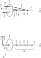
- FIG. 1 shows an example of an optical inspection system 100 for optically characterizing a sample 102, in accordance with some embodiments.
- the sample 102 is not part of the optical inspection system 100.
- the optical inspection system 100 of FIG. 1 is but one example; other suitable optical inspection systems can also be used.
- the optical inspection system 100 includes an illuminator/collector assembly 104.
- the illuminator/collector assembly 104 is a single objective lens.
- the illuminator/collector assembly 104 includes separate illumination optics and collection optics.
- the illuminator/collector assembly 104 delivers incident light 106 to the sample 102.
- the incident light 106 can have a range of propagation angles at the sample 102. In some examples, the range can have an angular width less than or equal to 20 degrees. In other examples, the range can have an angular width less than or equal to 10 degrees. In some of these examples, the incident light 106 can be collimated, with a range having an angular width of effectively zero. In examples exhibiting refraction at the sampling interface, due to differing indices of refraction, the angular width at the sampling interface can be defined in the medium having the larger range of angles.
- the incident light 106 includes more than one wavelength simultaneously, such as a plurality of discrete wavelengths or a relatively broad spectrum. In some examples, the incident light 106 includes one wavelength at a time, but the wavelength can be selectively shifted over time. In still other examples, the incident light 106 includes a relatively broad spectrum that shifts sequentially over time. In still other examples, the incident light 106 includes a plurality of relatively broad, non-overlapping spectral regions that all shift, together, over time. In some examples, the incident light 106 can be pulsed or modulated at one or more specified frequencies. In some examples, the incident light 106 can include multiple spectral regions, with each spectral regions being pulsed or modulated at its own unique frequency.
- the illuminator/collector assembly 104 can include one or more light sources, such as a single semiconductor laser, multiple semiconductor lasers having the same wavelength, multiple semiconductor lasers having different wavelengths, a single light emitting diode, multiple light emitting diodes having the same wavelength, multiple light emitting diodes having different wavelengths, one or more quantum cascade lasers, one or more superluminescent light sources, one or more amplified spontaneous emission sources, any combination of the above, or other suitable light sources.
- the illuminator/collector assembly 104 can further include one or more collimating and/or focusing optics, such as lenses, which can collimate and/or focus light produced by the one or more light sources.
- the illuminator/collector assembly 104 can further include one or more beam-steering elements, such as a beamsplitter, which can reflect an incident beam and transmit a collected beam, or can transmit an incident beam and reflect a collected beam.
- beam-steering elements such as a beamsplitter, which can reflect an incident beam and transmit a collected beam, or can transmit an incident beam and reflect a collected beam.
- the illuminator/collector assembly 104 can deliver the incident light 106 to the sample 102 through a sampling interface 108.
- the sampling interface 108 is a surface of an objective lens, the surface facing the sample 102.
- the sampling interface 108 can be an outward-facing surface of a device, which is placed into contact with the sample 102 during operation.
- the sampling interface 108 can be a cover glass, which is placed into contact with the sample 102 during operation.
- the sampling interface 108 can be a lens surface or an optical surface that is spaced apart in air or another incident medium from the sample 102.
- the sampling interface 108 can include separate first and second surfaces, where incident light passes through the first surface and return light passes through the second surface.
- the illuminator/collector assembly 104 can collect return light 110 returning from the sample 102 through the sampling interface 108 to form collected return light 112. In some examples, the incident light 106 and return light 110 pass through the same sampling interface 108.
- a sensor 114 can receive the collected return light 112. Unlike a conventional multi-pixel detector, which is largely insensitive to ray angle, the sensor 114 can measure ray intensities as a function of ray position and ray angle for the collected return light 112.
- the sensor 114 is a Shack-Hartmann sensor, which includes a microlens array 116 and a multi-pixel detector 118 at or near a focal plane of the microlens array 116.
- Another example of a suitable sensor 114 is an array of pinholes, with a multi-pixel detector disposed in an optical path after the array of pinholes. These are but two examples; other suitable sensors can also be used.
- the sensor 114 can produce a plurality of signals 120 corresponding to the measured ray intensities.
- the signals 120 are electrical.
- the signals 120 are optical, such as with optical intensities in an optical fiber.
- each pixel from the multi-pixel detector 118 can produce its own signal 120.
- one or more groups of pixels can be optically or electrically coupled together to form the signals 120.
- a computer 122 can receive the plurality of signals 120 from the sensor 114.
- the computer 122 can aggregate at least some of the received signals into a plurality of binned signals.
- Each binned signal can be formed from corresponding rays striking the sensor 114.
- Each of the corresponding rays traverses a respective optical path length within the sample 102.
- the optical path length traversed within the sample 102 by a ray of the incident light 106 is represented by the quantity A
- the optical path length traversed within the sample by a ray of the return light 110 is represented by the quantity B, so that the total optical path length traversed within the sample is represented by the quantity A+B.
- each binned signal can correspond to rays in the collected return light 112 that traverse within the sample 102 an estimated optical path length within a respective range of optical path lengths.
- the ranges of optical path length can be adjoining.
- the computer 122 includes a characterizer configured to determine a physical property 124 of the sample 102 based on the measured ray intensities as a function of ray positions and ray angles.
- the signals 120 can supply the ray intensities, ray positions, and ray angles to the computer 122.
- the characterizer can perform a first operation set using the first subset of rays and perform a second operation set using a second subset of rays in determining a physical property 124 of the sample 102.
- the subsets are determined by a ray selector (discussed below).
- the characterizer can fit the one or more of the signals to a Beer's Law calculation. In some of these examples, the characterizer can determine an absorptivity of the sample 102 based on the Beer's Law calculation. According to the present invention, the characterizer is configured to apply different weights to the signals when determining the absorptivity of the sample 102. Beer's Law describes how much light transmits through an absorptive or scattering sample.
- T ( ⁇ ) exp(- L ⁇ c ⁇ a ( ⁇ )), where ⁇ is the wavelength of light, L is the optical path length traversed within the sample by the light, a ( ⁇ ) is a wavelength-dependent absorptivity of a substance within the sample, c is a concentration of the substance within the sample, and T ( ⁇ ) is a fraction of light exiting the sample.
- the absorptivity is the output quantity from the optical inspection system 100.
- the output quantity can be functionally equivalent to absorptivity, such as transmissivity or complex refractive index.
- the absorptivity can be an intermediate quantity, which is used internally by the optical inspection system 100 to calculate one or more other physical properties of the sample 102, such as substance concentration, or other suitable physical properties.
- the optical inspection system can include a ray selector.
- the ray selector can select the first subset of rays from the collected return light 112 at the sensor 114 that meet a first selection criterion.
- the first selection criterion can include a first range of estimated path lengths, such as path lengths traversed within the sample 102 or path length distributions, such as distributions of path length traversed within the sample 102.
- the first selection criterion can include a first range of estimated ray penetration depths within the sample 102.
- the ray selector 116 can additionally select a second subset of rays from the collected return light 112 that meet a second selection criterion.
- the first and second selection criteria can include first and second ranges of estimated path lengths or path length distributions.
- the ray selector 116 can select more than two subsets of rays, with each subset having a corresponding selection criterion. Such subsets of rays can be referred to as bins, or binned rays.
- the ray selector can operate entirely in software.
- computer 122 can include a lookup table that maps each pixel at the multi-pixel detector 118 to a corresponding optical path traversed within the sample.
- the corresponding optical path within the sample can include ray position and ray angle at the sample 102 or at a suitable longitudinal location at or near the sample 102.
- Such a lookup table can be prepared by tracing rays through the geometry of the illuminator/collector 104 assembly and through any additional elements between the sample 102 and the sensor 114. Such a ray trace can be performed once, with the results being stored in the lookup table and accessible by the computer 122.
- the computer 122 can group the detector pixels into bins, with each bin corresponding to a specified range of optical path lengths traversed within the sample 102.
- the ray selector can receive signals from corresponding pixels of the detector 118, average a first subset of the signals to form a first binned signal, average a second subset of the signals to form the second binned signal, and average additional subsets of the signals to form additional binned signals.
- the computer 122 is configured to aggregate signals from the multi-pixel detector 118 into binned signals, each binned signal corresponding to rays in the collected return light that traverse within the sample an estimated optical path length within a respective range of optical path lengths. In some of these examples, the ranges of optical path length can adjoin one another.
- the ray selector can operate at least in part in hardware.
- at least some of the binning can occur at the hardware level.
- the detector area can instead be partitioned into shapes that correspond to the bins discussed above.
- each detector area can receive rays that traverse an optical path length within the sample, within a specified range of optical path lengths.
- each detector area can produce a respective signal 120, which is directed to the computer 122.
- the ray selector can include first and second pixels of the sensor, where the first and second pixels are shaped and sized to measure ray intensities for rays within the first and second subsets of rays.
- the first and second pixels can respectively output the first and second binned signals.
- the detector can use a grid of pixels, and each pixel can produce its own signal, but the signals are combined in hardware prior to delivery at the computer 122.
- the ray selector can operate in a combination of software and hardware, with some of the binning occurring at the sensor 114 and/or at the signal level, and some of the binning occurring at the computer 122.
- the reliability of the calculations can vary from location-to-location at the detector. For some geometries, such as the geometry associated with a single scattering event (discussed below in detail), the calculation can be relatively reliable.
- the optical inspection system 100 can set a specified threshold for reliability. Signals from detector locations exceeding the threshold can be used for subsequent calculations, and signals from detector locations below the threshold can be excluded from use in the subsequent calculations.
- the optical inspection system 100 can include an optional mask 126 positioned between the microlens array 116 and the multi-pixel detector 118. The mask 126 can block rays for which the optical inspection system 100 cannot reliably determine the optical path length traversed within the sample. In some examples, the mask 126 can be directly adjacent to, in contact with, or deposited on the multi-pixel detector 118. The mask 126 can include at least one blocking portion, which blocks specified rays in the collected return light 112. The mask 126 can block particular pixels on the multi-pixel detector 124.
- the mask 126 is stationary over time.
- the mask 126 can be formed as a coating on an optical surface, where the coating includes reflective, transmissive, and/or absorptive portions that do not change over time.
- the mask 126 can be reconfigurable over time.
- the mask 126 can be formed as a reconfigurable panel, such as an array of micromirrors, which can selectively direct portions of the collected return light 112 toward the detector 118 or away from the detector 118, and can change which portions are directed toward the detector 118 or away from the detector 118 as needed.
- the thresholding can be performed in combination with the computer 122 or entirely in software by the computer 122.
- the optical inspection system 100 assigns relative weights to the binned signals.
- Each weight can represent a confidence level that the optical path lengths within the sample 102 are the same, or are within a specified range for all of the rays in the corresponding bin.
- the relative weight varies inversely with a width of an estimated distribution of the respective optical path lengths for the binned signal.
- the term inverse is intended to signify a monotonic relationship between relative weight and distribution width, without requiring a mathematically proportional relationship. For instance, as the width of an estimated distribution decreases, the relative weight can increase. As another example, as the width of an estimated distribution increases, the relative weight can decrease.
- each of the corresponding rays when traced back through the illuminator/collector assembly 104, passes a respective distance away from a corresponding incident ray within the incident light, and the relative weight varies inversely with the respective distance.
- the weight of each binned signal corresponds to a probability that light that generated the binned signal originated from a single scattering event in the sample.
- FIGS 2-7 and the accompanying discussion below address the geometry of a single scattering event.
- the computer 122 can be included in a computer system that includes hardware, firmware and software. Binning electrical signals, assigning relative weight to the binned electrical signals, determining a physical property, as well as some intermediate computational tasks, such as tracing rays and characterizing, can be executed in software, or executed in digital electronic hardware in which the ray tracing and characterizing are hard-wired into the hardware; for the purposes of this document, such hard-wired digital electronic hardware is considered to be executing ray tracing software and/or a characterizer. Examples may also be implemented as instructions stored on a computer-readable storage device, which may be read and executed by at least one processor to perform the operations described herein.
- a computer-readable storage device may include any non-transitory mechanism for storing information in a form readable by a machine (e.g., a computer).
- a computer-readable storage device may include read-only memory (ROM), random-access memory (RAM), magnetic disk storage media, optical storage media, flash-memory devices, and other storage devices and media.
- computer systems can include one or more processors, optionally connected to a network, and may be configured with instructions stored on a computer-readable storage device.
- FIGS. 2-7 address a particular geometry associated with a single scattering event in the sample. For rays satisfying this geometry, the optical path traversed within the sample can be determined with a relatively high degree of confidence. It is instructive to explore the single scattering event geometry in detail.
- FIG. 2 shows a portion of an incident optical path in an example of an optical inspection system 200, in accordance with some embodiments.
- Incident light 208 from a light source 204 optionally redirected by a mirror, strikes a central portion of a pupil of an illuminator/collector assembly 206, and propagates within sample 202 generally coincident with a central axis 210 of the illuminator/collector assembly 206.
- the incident light 208 is shown in FIG. 2 as passing through three scattering events 212A, 212B, 212C.
- each of the scattering events 212A, 212B, 212C can redirect a fraction of the incident light 208 into a respective redirected ray, with the remaining fraction continuing to propagate away from the illuminator/collector assembly 206 along the central axis 210.
- the configuration of FIG. 2 and the use of three discrete scattering events, is but one example, and that other configurations can also be used.
- the incident optical path does not necessarily have to be coincident with the optical axis.
- FIG. 3 shows a portion of a return optical path in an example of an optical inspection system, in accordance with some embodiments.
- Elements numbered 300-312 in FIG. 3 are identical in structure and function to similarly numbered elements 200-212 in FIG. 2 .
- Light rays 314A, 314B, 314C arise from respective scattering events 312A, 312B, 312C.
- the illuminator/collector 306 collects and redirects rays 314A, 314B, 314C to form return rays 316A, 316B, 316C.
- FIGS. 4A, 4B, and 4C are individual views of the three light rays in the return optical path of FIG. 3 , in accordance with some embodiments. Because rays 416A, 416B, 416C originate from points along the central axis 410 of the illuminator/collector assembly 406, rays 416A, 416B, 416C propagate within respective planes 418A, 418B, 418C, all of which include the central axis 410 of the illuminator/collector 406.
- FIG. 5 shows the rays of FIGS. 4A, 4B, and 4C , traced from the illuminator/collector assembly 506, to the array 520 of microlenses 522, to the detector 528, in accordance with some embodiments.
- the detector 528 can include a plurality of zones 530 in a one-to-one correspondence with the array 520 of microlenses 522. Each zone 530 can have a center 532 corresponding to a center 524 of a respective microlens 522.
- the array 520 of microlenses 522 redirects rays 516A, 516B, 516C to form rays 526A, 526B, 526C, which strike detector 528 at locations 534A, 534B, 534C.
- FIG. 6 shows an end-on view of the detector 628 from FIG. 5 , in accordance with some embodiments.
- Each zone 630 can include a respective region 636 at which rays propagating from the sample to the Shack-Hartmann sensor propagate in a plane that includes the central axis of the illuminator/collector assembly.
- the regions 636 can be linear, can be radially oriented with respect to the central axis of the illuminator/collector assembly or a center 638 of the detector 628, and can include a center 632 of the respective zone 630.
- Rays 526A, 526B, 526C strike the detector 628 at respective locations 634A, 634B, 634C.
- a distance away from the zone center 632 can be proportional to (or nearly proportional to, or related with a 1:1 correspondence to) a propagation angle of rays 516A, 516B, 516C ( FIG. 5 ).
- Other possible arrangements include an input light that propagates in a direction, which is not coincident with a central axis of the optical inspection system.
- the rays can be traced back through the illuminator/collector assembly, and can intersect corresponding incident rays within the incident light.
- the incident light can have a range of propagation angles at the sampling interface, where the range can have an angular width less than or equal to 20 degrees, or preferably less than or equal to 10 degrees. As the angular range increases, it becomes more difficult to accurately determine the optical path length traversed within the sample.
- the ray paths can be used to calculate respective optical path lengths traversed within the sample.
- the ray intensities can be correlated with the optical path lengths.
- the correlation can be used to determine a physical property of the sample, such as absorptivity, transmissivity, refractive index, and others.
- the optical path lengths cannot easily be calculated.
- the propagation angle and location of a particular ray in the collected return light can determine whether or not the particular ray resides in a plane that includes the central axis (or, alternatively, the direction of the incident optical path). If the propagation angle and location of the ray show that the ray resides in one of said planes, then the contribution from the ray can be weighted relatively heavily to be used downstream to calculate the physical property of the sample. If the propagation angle and location of the ray show that the ray does not reside in one of said planes, then the contribution from the particular ray can be weighted relatively lightly to be used downstream to calculate the physical property of the sample.
- One way to determine whether a particular ray resides in a plane that includes the central axis is to trace the ray backwards, through the illuminator/collector assembly, to the sample. There will be a particular longitudinal location at which the traced ray is a minimum distance from the central axis. This minimum distance for each traced ray can be used to determine a weight, such as relative weight, which indicates how confidently one can determine the optical path length traversed in the sample by the traced ray. If the traced ray intersects the central axis, the minimum distance is zero, and the weighting factor can be its maximum value. If the traced ray comes relatively close to the central axis, the weighting factor can be relatively high. If the traced ray passes relatively far from the central axis, the weighting factor can be relatively low. In some examples, the weighting factor for a traced ray can vary inversely with a minimum distance between the traced ray and the central axis.
- the identified region or regions can correspond to one or more detector regions at which a confidence level of an estimated optical path length falls below a threshold value.
- Other suitable ways to determine the identified detector regions can also be used.
- rays in the one or more identified detector regions can be weighted more lightly than rays outside the identified detector regions, when determining the physical property of the sample.
- each detector pixel, or suitable group of detector pixels can be assigned a relative weight.
- the relative weight can represent a confidence level that the optical path lengths within the sample are the same.
- the relative weight can represent a confidence level that the optical path lengths are similar, or are nearly the same, or span a range with a width that is within a specified percentage of the mean optical path length traversed within the sample for all the rays included in the respective bin.
- the relative weight can vary inversely with a width of an estimated distribution of the respective optical path lengths within the sample.
- each ray in the collected light when traced back through an illuminator/collector assembly, passes a respective distance away from a corresponding incident ray within the incident light, and the relative weight can vary inversely with the respective distance.
- the relative weight can correspond to a probability that corresponding rays originated from a single scattering event in the sample. Other weighting schemes are also possible.
- rays in the one or more identified detector regions can be excluded entirely when determining the physical property of the sample.
- the exclusion can be performed in software, such as by a computer, such as 122 ( FIG. 1 ). In other examples, the exclusion can be performed entirely in hardware, such as with a mask, such as 126 ( FIG. 1 ).
- FIG. 7 shows an end-on view of an example of a mask 700 disposed proximate the detector of FIG. 6 in the Shack-Hartmann sensor, in accordance with some embodiments.
- Mask 700 blocks portions 1002 and transmits portions 1004 to the detector.
- the mask 700 pass only rays that, when traced backward through the illuminator/collector assembly, pass within a threshold distance of the central axis of the illuminator/collector assembly.
- One bin, corresponding to rays that fall within transmitted portion 704 is used to calculate the physical property of the sample.
- This bin can have a relative weight of 100%, or another suitable measure.
- the other bin, corresponding to rays that fall within blocked portion 702 is not used to calculate the physical property of the sample.
- This bin can have a relative weight of 0%, or another suitable measure.
- the detector can be a multi-pixel detector, with pixels arranged in a rectangular pattern, and each pixel producing a corresponding electrical signal.
- the detector can be a multi-element detector, with regions having any suitable sizes and shapes, and each region producing a corresponding electrical signal.
- the detector can be a single-element detector, producing a single electrical signal.
- FIG. 8 shows a flow chart of an example of a method 800 for optically characterizing a sample, in accordance with some embodiments.
- the method 800 can be executed on an optical inspection system, such as 100 ( FIG. 1 ).
- Method 800 is but one example; other suitable methods for optically inspecting a sample can also be used.
- method 800 illuminates the sample with incident light.
- method 800 collects return light returning from the sample to form collected return light.
- method 800 measures ray intensities as a function of ray position and ray angle for the collected return light.
- method 800 aggregates at least some of the electrical signals into a plurality of binned signals. The aggregation into bins can be performed purely in software, purely in hardware, or in a combination of software and hardware.
- method 800 determining a physical property of the sample based on the binned signals.
- each binned signal can correspond to rays in the collected return light that traverse within the sample an estimated optical path length within a respective range of optical path lengths.
- method 800 can further include fitting the binned signals to a Beer's Law calculation; and determining an absorptivity of the sample based on the Beer's Law calculation.
- the optical properties of a particular type of sample can vary from sample-to-sample, but often fall into a well-defined range of numerical values.
- a scattering coefficient of a particular sample typically falls within a particular range of scattering coefficients, where the range can represent a distribution of values of the scattering coefficient for a population of samples of the same type as the particular sample.
- the range can be centered around a so-called expected value, such as an expected scattering coefficient.
- the expected values can be used when designing a geometry for an optical inspection system, with the expectation that most actual measured values will be relatively close to, but different from, the expected value.
- sample-to-sample variation of a scattering and/or absorption coefficient can produce a sample-to-sample variation in the optical power reaching a detector.
- sample-to-sample variation can be undesirable, and can underutilize a full dynamic range of the detector. It is possible to design the optical inspection system to have a decreased sensitivity of detected optical power to sample-to-sample variation in scattering coefficient.
- An analytical model of the optical inspection system can assume that a light ray enters the sample at an input point, scatters a single time at a scattering location, changes direction just once at the scattering location, and exits the sample at an output point.
- an input beam is attenuated by a factor exp[-A( ⁇ s + ⁇ a )], where quantities ⁇ s and ⁇ a are the scattering and absorption coefficients of the sample, respectively, and quantity A is an optical path length between the input point and the scattering location.
- ⁇ s and ⁇ a are the scattering and absorption coefficients of the sample, respectively
- quantity A is an optical path length between the input point and the scattering location.
- a fraction ⁇ s of the remaining input beam is scattered towards the output, where factor ⁇ accounts for a scattering phase function.
- the light scattered toward the output location is further attenuated by an amount exp[-B( ⁇ s + ⁇ a )] before exiting the sample, where quantity B is an optical path length between the scattering location and the output point.
- a fraction of optical power exiting the sample at the output location, divided by optical power entering the sample at the input location, is given by the quantity ⁇ s exp[-L( ⁇ s + ⁇ a )], where quantity L equals quantity A+B, and is a total optical path length traversed within the sample.
- the fraction of optical power exiting the sample is relatively insensitive when its derivative equals zero, e.g., when the total optical path length traversed within the sample, L, equals an inverse of the scattering coefficient of the sample, 1/ ⁇ s .
- L 1/ ⁇ s
- the optical power reaching the detector is maximized, which is beneficial, and is relatively insensitive to sample-to-sample variations in the amount of scattering, which is also beneficial.
- the optical inspection system can be designed so that a total optical path length traversed within the sample can equal, or can be relatively close to, an inverse of an expected scattering coefficient of the sample.
- the total optical path length traversed within the sample can be within 0.1%, within 1%, within 10%, or within 50% of an inverse of an expected scattering coefficient of the sample.
- Other suitable values can also be used.
- the expected scattering coefficient can represent a distribution of values of the scattering coefficient for a population of samples of the same type as the particular sample, such as human tissue.
- the above analysis assumes a single scattering event within the sample. For geometries in which a detector element receives light that is largely due to a single high-angle scattering event, the above analysis also holds for multiple scattering events and finite positional and angular resolutions. The above analysis can also apply to confocal detection with a narrow collimated input and angularly-constrained output.
Description
- The present disclosure relates to an optical inspection system for optically characterizing a sample, which can account for variations of optical path length within the sample.
- Many optical inspection systems deliver light to a sample, collect light reflected or scattered from the sample, and use the collected light to analyze a portion of the sample. It can be desirable to improve these optical inspection systems.
-
US 2010/225913 A1 discloses an instrument for measuring characteristics of a particle sample by counting and classifying particles into selected ranges of particle characteristics. The particle concentration is reduced to the level where the probability of measuring scattering from multiple particles of interest at one time is reduced to an acceptable level. A light beam is projected through a sample space, through which the particles flow. As each particle passes through the beam, it scatters, absorbs, and transmits different amounts of the light, depending upon the particle characteristics. So both the decrease in the beam intensity, due to light removal by the particle, and light scattered by the particle, may be used to determine the particle characteristics, to classify the particle and count it in a certain range of particle characteristics. In one example, a detector is disclosed, which has wedge shaped detector elements so as to progressively weight different scattering angles. -
WO 2006/086566 A2 discloses a family of methods for measuring with relatively high accuracy analyte concentrations in samples that both absorb and scatter light. Methods for determining analyte concentrations in a sample from one or more optical measurements are disclosed. The methods take into account different path lengths of light which is scattered in the samples and predict analyte concentrations based on Beer's law. -
US 2011/184260 A1 discloses noninvasive glucose monitoring. Source light is transmitted through an illumination polarizer to the tissue, e.g. a finger. The input light, containing multiple wavelengths, is diffusely scattered by the tissue, with a portion of the light being returned back. The returning light contains photons whose polarization has not been altered as well as photons whose polarization has been changed through a scattering event. The light maintaining the polarization of the input polarizer consists of the superficially reflected light plus one half of the deeply penetrating light that has penetrated the tissue and experienced a scattering event that has altered the original polarization. The light returned from the tissue contains both polarization states. An analyzing polarizer can be rotated so as to preferentially select those photons maintaining the input polarization or for those photons whose polarization has been modified. The angle between the illumination and collection polarizer can be varied to any desired angle but for the preferential selection of glucose containing photons a 90° angle is used. Because tissue is a scattering medium, light entering the tissue from a light source must generally undergo one or more scattering events to reverse direction and exit the tissue to be collected by the detector. When polarized light undergoes a scattering event it becomes partially depolarized, i.e. a portion of the light can become randomly polarized while another portion of the light might maintains its original state of polarization. The expected path length distribution for several orientations of the analyzer is taken into account when determining the spectral absorption. -
US 2014/043620 A1 discloses the determination of light absorption in a scattering medium using different light path models for light paths in the medium along which light reaches different positions of an image sensor. - The object of the invention is solved by the features of the independent claims. The dependent claims are directed to preferred embodiments of the invention.
- An illuminator/collector assembly can deliver incident light to a sample and collect return light returning from the sample. A sensor, such as a Shack-Hartmann sensor, can measure ray intensities as a function of ray position and ray angle for the collected return light. A ray selector can select a first subset of rays from the collected return light at the sensor that meet a first selection criterion. In some examples, the ray selector can aggregate rays into binned signals, each binned signal corresponding to rays in the collected return light that traverse within the sample an estimated optical path length within a respective range of optical path lengths. A characterizer can determine a physical property of the sample, such as absorptivity, based on the ray intensities, ray positions, and ray angles for the first subset of rays. Accounting for variations in optical path length traversed within the sample can improve accuracy.
- In the drawings, which are not necessarily drawn to scale, like numerals may describe similar components in different views. Like numerals having different letter suffixes may represent different instances of similar components. The drawings illustrate generally, by way of example, but not by way of limitation, various examples discussed in the present document.
- The present invention is defined in claims 1 and 12.
-
FIG. 1 shows an example of an optical inspection system for optically characterizing a sample, in accordance with some embodiments. -
FIG. 2 shows a portion of an incident optical path in an example of an optical inspection system, in accordance with some embodiments. -
FIG. 3 shows a portion of a return optical path in an example of an optical inspection system, in accordance with some embodiments. -
FIGS. 4A, 4B, and 4C are individual views of the three light rays in the return optical path ofFIG. 3 , in accordance with some embodiments. -
FIG. 5 shows the rays ofFIGS. 4A, 4B, and 4C , traced from the illuminator/collector assembly, to the array of microlenses, to the detector, in accordance with some embodiments. -
FIG. 6 shows an end-on view of the detector fromFIG. 5 , in accordance with some embodiments. -
FIG. 7 shows an end-on view of an example of a mask disposed proximate the detector ofFIG. 6 , in accordance with some embodiments. -
FIG. 8 shows a flow chart of an example of a method for optically characterizing a sample, in accordance with some embodiments. - An optical inspection system can deliver light to a sample, collect light reflected or scattered from the sample, use the collected light to determine a physical property of the sample, such as absorptivity or refractive index. For highly absorbing or scattering samples, the high absorption or scattering can reduce an intensity of a light ray propagating through a portion of the sample. This reduction in intensity can depend strongly on the optical path length traversed within the sample.
- For instance, in some configurations that deliver light to a sample and collect light reflected from the sample, the illuminating light is delivered as cone of light, converging toward a particular location at or below a surface of the sample. Similarly, the collected light is retrieved from a cone of light, diverging away from the particular location in the sample. For these cones of light, different portions of the cone can traverse different optical path lengths within the sample. For instance, a light ray at the center of the cone can traverse an optical path within the sample that is shorter than a light ray at the edge of the cone.
- The optical inspection system can account for differences in the optical path length traversed within the sample, as a function of ray location and angle within the collected light. For some samples, an incident light ray is likely to be redirected by a single scattering event within the sample, such as a reflection or a redirection from a particular particle within the sample, or from an interface between two internal structures within the sample.
- For these samples, the optical inspection system can use the geometry of single scattering events to determine regions on a detector at which the optical path length traversed within the sample can be determined relatively accurately. For these regions, a ray striking the region can have a known optical path length within the sample, or can have a relatively tight distribution of optical path lengths within the sample. For instance, the regions can describe locations on the detector at which rays returning from the sample arise from a single scattering event within the sample. According to the present invention, these detector regions are weighted relatively strongly when determining the physical property of the sample. The detector regions can be selected as a function of sample type, to best use available dynamic ranges of detector pixels, and so forth.
- Similarly, the detector can have regions at which the optical path length traversed within the sample cannot be determined accurately. For these regions, a ray striking the region can have one of many optical path lengths within the sample, or can have a relatively broad distribution of optical path lengths within the sample. For instance, the regions can describe locations on the detector at which rays returning from the sample arise from multiple sequential scattering events within the sample. For these multiply scattered rays, there may be many possible paths within the sample. According to the present invention, these detector regions are weighted relatively weakly or excluded when determining the physical property of the sample.
-
FIG. 1 shows an example of anoptical inspection system 100 for optically characterizing asample 102, in accordance with some embodiments. Thesample 102 is not part of theoptical inspection system 100. Theoptical inspection system 100 ofFIG. 1 is but one example; other suitable optical inspection systems can also be used. - The
optical inspection system 100 includes an illuminator/collector assembly 104. In some examples, the illuminator/collector assembly 104 is a single objective lens. In other examples, the illuminator/collector assembly 104 includes separate illumination optics and collection optics. - The illuminator/
collector assembly 104 delivers incident light 106 to thesample 102. Theincident light 106 can have a range of propagation angles at thesample 102. In some examples, the range can have an angular width less than or equal to 20 degrees. In other examples, the range can have an angular width less than or equal to 10 degrees. In some of these examples, theincident light 106 can be collimated, with a range having an angular width of effectively zero. In examples exhibiting refraction at the sampling interface, due to differing indices of refraction, the angular width at the sampling interface can be defined in the medium having the larger range of angles. In some examples, theincident light 106 includes more than one wavelength simultaneously, such as a plurality of discrete wavelengths or a relatively broad spectrum. In some examples, theincident light 106 includes one wavelength at a time, but the wavelength can be selectively shifted over time. In still other examples, theincident light 106 includes a relatively broad spectrum that shifts sequentially over time. In still other examples, theincident light 106 includes a plurality of relatively broad, non-overlapping spectral regions that all shift, together, over time. In some examples, theincident light 106 can be pulsed or modulated at one or more specified frequencies. In some examples, theincident light 106 can include multiple spectral regions, with each spectral regions being pulsed or modulated at its own unique frequency. In some examples, the illuminator/collector assembly 104 can include one or more light sources, such as a single semiconductor laser, multiple semiconductor lasers having the same wavelength, multiple semiconductor lasers having different wavelengths, a single light emitting diode, multiple light emitting diodes having the same wavelength, multiple light emitting diodes having different wavelengths, one or more quantum cascade lasers, one or more superluminescent light sources, one or more amplified spontaneous emission sources, any combination of the above, or other suitable light sources. In some examples, the illuminator/collector assembly 104 can further include one or more collimating and/or focusing optics, such as lenses, which can collimate and/or focus light produced by the one or more light sources. In some examples, the illuminator/collector assembly 104 can further include one or more beam-steering elements, such as a beamsplitter, which can reflect an incident beam and transmit a collected beam, or can transmit an incident beam and reflect a collected beam. - The illuminator/
collector assembly 104 can deliver the incident light 106 to thesample 102 through asampling interface 108. In the specific example ofFIG. 1 , thesampling interface 108 is a surface of an objective lens, the surface facing thesample 102. In some examples, thesampling interface 108 can be an outward-facing surface of a device, which is placed into contact with thesample 102 during operation. In some examples, thesampling interface 108 can be a cover glass, which is placed into contact with thesample 102 during operation. In some examples, thesampling interface 108 can be a lens surface or an optical surface that is spaced apart in air or another incident medium from thesample 102. In some examples, thesampling interface 108 can include separate first and second surfaces, where incident light passes through the first surface and return light passes through the second surface. - The illuminator/
collector assembly 104 can collect return light 110 returning from thesample 102 through thesampling interface 108 to form collectedreturn light 112. In some examples, theincident light 106 and return light 110 pass through thesame sampling interface 108. - A
sensor 114 can receive the collectedreturn light 112. Unlike a conventional multi-pixel detector, which is largely insensitive to ray angle, thesensor 114 can measure ray intensities as a function of ray position and ray angle for the collectedreturn light 112. In the example ofFIG. 1 , thesensor 114 is a Shack-Hartmann sensor, which includes amicrolens array 116 and amulti-pixel detector 118 at or near a focal plane of themicrolens array 116. Another example of asuitable sensor 114 is an array of pinholes, with a multi-pixel detector disposed in an optical path after the array of pinholes. These are but two examples; other suitable sensors can also be used. - The
sensor 114 can produce a plurality ofsignals 120 corresponding to the measured ray intensities. In some examples, thesignals 120 are electrical. In other examples, thesignals 120 are optical, such as with optical intensities in an optical fiber. In some examples, each pixel from themulti-pixel detector 118 can produce itsown signal 120. In other examples, one or more groups of pixels can be optically or electrically coupled together to form thesignals 120. - A
computer 122 can receive the plurality ofsignals 120 from thesensor 114. In some examples, thecomputer 122 can aggregate at least some of the received signals into a plurality of binned signals. Each binned signal can be formed from corresponding rays striking thesensor 114. Each of the corresponding rays traverses a respective optical path length within thesample 102. In the example ofFIG. 1 , the optical path length traversed within thesample 102 by a ray of theincident light 106 is represented by the quantity A, and the optical path length traversed within the sample by a ray of thereturn light 110 is represented by the quantity B, so that the total optical path length traversed within the sample is represented by the quantity A+B. In some examples, it can be advantageous if the quantity A+B equals, or is on the order of, an inverse of an expected absorption coefficient of thesample 102; the Appendix discusses this in detail. For the binned signals, each binned signal can correspond to rays in the collected return light 112 that traverse within thesample 102 an estimated optical path length within a respective range of optical path lengths. In some examples, the ranges of optical path length can be adjoining. - According to the present invention, the
computer 122 includes a characterizer configured to determine aphysical property 124 of thesample 102 based on the measured ray intensities as a function of ray positions and ray angles. Thesignals 120 can supply the ray intensities, ray positions, and ray angles to thecomputer 122. In some examples, the characterizer can perform a first operation set using the first subset of rays and perform a second operation set using a second subset of rays in determining aphysical property 124 of thesample 102. The subsets are determined by a ray selector (discussed below). - In some examples, the characterizer can fit the one or more of the signals to a Beer's Law calculation. In some of these examples, the characterizer can determine an absorptivity of the
sample 102 based on the Beer's Law calculation. According to the present invention, the characterizer is configured to apply different weights to the signals when determining the absorptivity of thesample 102. Beer's Law describes how much light transmits through an absorptive or scattering sample. One example of a configuration for Beer's Law is T(λ) = exp(-L×c×a(λ)), where λ is the wavelength of light, L is the optical path length traversed within the sample by the light, a(λ) is a wavelength-dependent absorptivity of a substance within the sample, c is a concentration of the substance within the sample, and T(λ) is a fraction of light exiting the sample. Other suitable configurations of Beer's Law can also be used. In some examples, the absorptivity is the output quantity from theoptical inspection system 100. In other examples, the output quantity can be functionally equivalent to absorptivity, such as transmissivity or complex refractive index. In other examples, the absorptivity can be an intermediate quantity, which is used internally by theoptical inspection system 100 to calculate one or more other physical properties of thesample 102, such as substance concentration, or other suitable physical properties. - The optical inspection system can include a ray selector. The ray selector can select the first subset of rays from the collected return light 112 at the
sensor 114 that meet a first selection criterion. In some examples, the first selection criterion can include a first range of estimated path lengths, such as path lengths traversed within thesample 102 or path length distributions, such as distributions of path length traversed within thesample 102. In other examples, the first selection criterion can include a first range of estimated ray penetration depths within thesample 102. In some examples, theray selector 116 can additionally select a second subset of rays from the collected return light 112 that meet a second selection criterion. For these examples, the first and second selection criteria can include first and second ranges of estimated path lengths or path length distributions. In other examples, theray selector 116 can select more than two subsets of rays, with each subset having a corresponding selection criterion. Such subsets of rays can be referred to as bins, or binned rays. - In some examples, the ray selector can operate entirely in software. For instance,
computer 122 can include a lookup table that maps each pixel at themulti-pixel detector 118 to a corresponding optical path traversed within the sample. The corresponding optical path within the sample can include ray position and ray angle at thesample 102 or at a suitable longitudinal location at or near thesample 102. Such a lookup table can be prepared by tracing rays through the geometry of the illuminator/collector 104 assembly and through any additional elements between thesample 102 and thesensor 114. Such a ray trace can be performed once, with the results being stored in the lookup table and accessible by thecomputer 122. From the lookup table, thecomputer 122 can group the detector pixels into bins, with each bin corresponding to a specified range of optical path lengths traversed within thesample 102. In some examples, the ray selector can receive signals from corresponding pixels of thedetector 118, average a first subset of the signals to form a first binned signal, average a second subset of the signals to form the second binned signal, and average additional subsets of the signals to form additional binned signals. In some examples, thecomputer 122 is configured to aggregate signals from themulti-pixel detector 118 into binned signals, each binned signal corresponding to rays in the collected return light that traverse within the sample an estimated optical path length within a respective range of optical path lengths. In some of these examples, the ranges of optical path length can adjoin one another. - In other examples, the ray selector can operate at least in part in hardware. For these examples, at least some of the binning can occur at the hardware level. For instance, instead of using a grid of pixels at the detector, the detector area can instead be partitioned into shapes that correspond to the bins discussed above. In this example, each detector area can receive rays that traverse an optical path length within the sample, within a specified range of optical path lengths. In some of these examples, each detector area can produce a
respective signal 120, which is directed to thecomputer 122. In some examples, the ray selector can include first and second pixels of the sensor, where the first and second pixels are shaped and sized to measure ray intensities for rays within the first and second subsets of rays. For these examples, the first and second pixels can respectively output the first and second binned signals. As another example, the detector can use a grid of pixels, and each pixel can produce its own signal, but the signals are combined in hardware prior to delivery at thecomputer 122. - In still other examples, the ray selector can operate in a combination of software and hardware, with some of the binning occurring at the
sensor 114 and/or at the signal level, and some of the binning occurring at thecomputer 122. - For each location at the
detector 118, it can be possible to calculate a corresponding estimated optical path traversed within the sample. However, the reliability of the calculations can vary from location-to-location at the detector. For some geometries, such as the geometry associated with a single scattering event (discussed below in detail), the calculation can be relatively reliable. - In some examples, the
optical inspection system 100 can set a specified threshold for reliability. Signals from detector locations exceeding the threshold can be used for subsequent calculations, and signals from detector locations below the threshold can be excluded from use in the subsequent calculations. For some of these examples, theoptical inspection system 100 can include anoptional mask 126 positioned between themicrolens array 116 and themulti-pixel detector 118. Themask 126 can block rays for which theoptical inspection system 100 cannot reliably determine the optical path length traversed within the sample. In some examples, themask 126 can be directly adjacent to, in contact with, or deposited on themulti-pixel detector 118. Themask 126 can include at least one blocking portion, which blocks specified rays in the collectedreturn light 112. Themask 126 can block particular pixels on themulti-pixel detector 124. In some examples, themask 126 is stationary over time. For instance, themask 126 can be formed as a coating on an optical surface, where the coating includes reflective, transmissive, and/or absorptive portions that do not change over time. In other examples, themask 126 can be reconfigurable over time. For instance, themask 126 can be formed as a reconfigurable panel, such as an array of micromirrors, which can selectively direct portions of the collected return light 112 toward thedetector 118 or away from thedetector 118, and can change which portions are directed toward thedetector 118 or away from thedetector 118 as needed. Alternatively, the thresholding can be performed in combination with thecomputer 122 or entirely in software by thecomputer 122. - According to the present invention, rather than use a single threshold value, the
optical inspection system 100 assigns relative weights to the binned signals. Each weight can represent a confidence level that the optical path lengths within thesample 102 are the same, or are within a specified range for all of the rays in the corresponding bin. In some examples, the relative weight varies inversely with a width of an estimated distribution of the respective optical path lengths for the binned signal. In these examples, the term inverse is intended to signify a monotonic relationship between relative weight and distribution width, without requiring a mathematically proportional relationship. For instance, as the width of an estimated distribution decreases, the relative weight can increase. As another example, as the width of an estimated distribution increases, the relative weight can decrease. In some examples, each of the corresponding rays, when traced back through the illuminator/collector assembly 104, passes a respective distance away from a corresponding incident ray within the incident light, and the relative weight varies inversely with the respective distance. In some examples, the weight of each binned signal corresponds to a probability that light that generated the binned signal originated from a single scattering event in the sample.FIGS 2-7 and the accompanying discussion below address the geometry of a single scattering event. - The
computer 122 can be included in a computer system that includes hardware, firmware and software. Binning electrical signals, assigning relative weight to the binned electrical signals, determining a physical property, as well as some intermediate computational tasks, such as tracing rays and characterizing, can be executed in software, or executed in digital electronic hardware in which the ray tracing and characterizing are hard-wired into the hardware; for the purposes of this document, such hard-wired digital electronic hardware is considered to be executing ray tracing software and/or a characterizer. Examples may also be implemented as instructions stored on a computer-readable storage device, which may be read and executed by at least one processor to perform the operations described herein. A computer-readable storage device may include any non-transitory mechanism for storing information in a form readable by a machine (e.g., a computer). For example, a computer-readable storage device may include read-only memory (ROM), random-access memory (RAM), magnetic disk storage media, optical storage media, flash-memory devices, and other storage devices and media. In some examples, computer systems can include one or more processors, optionally connected to a network, and may be configured with instructions stored on a computer-readable storage device. -
FIGS. 2-7 address a particular geometry associated with a single scattering event in the sample. For rays satisfying this geometry, the optical path traversed within the sample can be determined with a relatively high degree of confidence. It is instructive to explore the single scattering event geometry in detail. -
FIG. 2 shows a portion of an incident optical path in an example of anoptical inspection system 200, in accordance with some embodiments. Incident light 208 from alight source 204, optionally redirected by a mirror, strikes a central portion of a pupil of an illuminator/collector assembly 206, and propagates withinsample 202 generally coincident with acentral axis 210 of the illuminator/collector assembly 206. Theincident light 208 is shown inFIG. 2 as passing through three scatteringevents events collector assembly 206 along thecentral axis 210. It will be understood that the configuration ofFIG. 2 , and the use of three discrete scattering events, is but one example, and that other configurations can also be used. It will also be understood that the incident optical path does not necessarily have to be coincident with the optical axis. -
FIG. 3 shows a portion of a return optical path in an example of an optical inspection system, in accordance with some embodiments. Elements numbered 300-312 inFIG. 3 are identical in structure and function to similarly numbered elements 200-212 inFIG. 2 . Light rays 314A, 314B, 314C arise fromrespective scattering events collector 306 collects and redirectsrays return rays -
FIGS. 4A, 4B, and 4C are individual views of the three light rays in the return optical path ofFIG. 3 , in accordance with some embodiments. Becauserays central axis 410 of the illuminator/collector assembly 406,rays respective planes central axis 410 of the illuminator/collector 406. -
FIG. 5 shows the rays ofFIGS. 4A, 4B, and 4C , traced from the illuminator/collector assembly 506, to thearray 520 ofmicrolenses 522, to thedetector 528, in accordance with some embodiments. Thedetector 528 can include a plurality ofzones 530 in a one-to-one correspondence with thearray 520 ofmicrolenses 522. Eachzone 530 can have acenter 532 corresponding to acenter 524 of arespective microlens 522. Thearray 520 ofmicrolenses 522 redirects rays 516A, 516B, 516C to formrays detector 528 atlocations -
FIG. 6 shows an end-on view of thedetector 628 fromFIG. 5 , in accordance with some embodiments. Eachzone 630 can include arespective region 636 at which rays propagating from the sample to the Shack-Hartmann sensor propagate in a plane that includes the central axis of the illuminator/collector assembly. Theregions 636 can be linear, can be radially oriented with respect to the central axis of the illuminator/collector assembly or acenter 638 of thedetector 628, and can include acenter 632 of therespective zone 630.Rays FIG. 5 ) strike thedetector 628 atrespective locations zone center 632 can be proportional to (or nearly proportional to, or related with a 1:1 correspondence to) a propagation angle ofrays FIG. 5 ). Other possible arrangements include an input light that propagates in a direction, which is not coincident with a central axis of the optical inspection system. - In an alternate configuration, where the incident light has a slightly larger footprint and extends over an area that can include the central axis, the rays can be traced back through the illuminator/collector assembly, and can intersect corresponding incident rays within the incident light. For some of these configurations, the incident light can have a range of propagation angles at the sampling interface, where the range can have an angular width less than or equal to 20 degrees, or preferably less than or equal to 10 degrees. As the angular range increases, it becomes more difficult to accurately determine the optical path length traversed within the sample.
- For rays that reside in (or sufficiently near) a plane that includes the central axis of the illuminator/collector assembly, the ray paths can be used to calculate respective optical path lengths traversed within the sample. The ray intensities can be correlated with the optical path lengths. The correlation can be used to determine a physical property of the sample, such as absorptivity, transmissivity, refractive index, and others. For other rays, which do not reside in (or sufficiently near) said planes, the optical path lengths cannot easily be calculated.
- The propagation angle and location of a particular ray in the collected return light, such as 310 (
FIG. 3 ) or 410 (FIG. 4 ), can determine whether or not the particular ray resides in a plane that includes the central axis (or, alternatively, the direction of the incident optical path). If the propagation angle and location of the ray show that the ray resides in one of said planes, then the contribution from the ray can be weighted relatively heavily to be used downstream to calculate the physical property of the sample. If the propagation angle and location of the ray show that the ray does not reside in one of said planes, then the contribution from the particular ray can be weighted relatively lightly to be used downstream to calculate the physical property of the sample. - One way to determine whether a particular ray resides in a plane that includes the central axis is to trace the ray backwards, through the illuminator/collector assembly, to the sample. There will be a particular longitudinal location at which the traced ray is a minimum distance from the central axis. This minimum distance for each traced ray can be used to determine a weight, such as relative weight, which indicates how confidently one can determine the optical path length traversed in the sample by the traced ray. If the traced ray intersects the central axis, the minimum distance is zero, and the weighting factor can be its maximum value. If the traced ray comes relatively close to the central axis, the weighting factor can be relatively high. If the traced ray passes relatively far from the central axis, the weighting factor can be relatively low. In some examples, the weighting factor for a traced ray can vary inversely with a minimum distance between the traced ray and the central axis.
- In some examples, it can be beneficial to identify one or more detector regions, where it can be difficult to reliably determine an estimated optical path length traversed within the sample for a ray striking an identified region. For instance, the identified region or regions can correspond to one or more detector regions at which a confidence level of an estimated optical path length falls below a threshold value. Other suitable ways to determine the identified detector regions can also be used.
- In some examples, rays in the one or more identified detector regions can be weighted more lightly than rays outside the identified detector regions, when determining the physical property of the sample. For instance, each detector pixel, or suitable group of detector pixels, can be assigned a relative weight. In some examples, the relative weight can represent a confidence level that the optical path lengths within the sample are the same. In some examples, the relative weight can represent a confidence level that the optical path lengths are similar, or are nearly the same, or span a range with a width that is within a specified percentage of the mean optical path length traversed within the sample for all the rays included in the respective bin. In other examples, the relative weight can vary inversely with a width of an estimated distribution of the respective optical path lengths within the sample. In still other examples, each ray in the collected light, when traced back through an illuminator/collector assembly, passes a respective distance away from a corresponding incident ray within the incident light, and the relative weight can vary inversely with the respective distance. In still other examples, the relative weight can correspond to a probability that corresponding rays originated from a single scattering event in the sample. Other weighting schemes are also possible.
- In some examples, rays in the one or more identified detector regions can be excluded entirely when determining the physical property of the sample. One can consider this exclusion to be an extreme weighting, where excluded rays are assigned a weight of zero. In some examples, the exclusion can be performed in software, such as by a computer, such as 122 (
FIG. 1 ). In other examples, the exclusion can be performed entirely in hardware, such as with a mask, such as 126 (FIG. 1 ). -
FIG. 7 shows an end-on view of an example of amask 700 disposed proximate the detector ofFIG. 6 in the Shack-Hartmann sensor, in accordance with some embodiments. Mask 700 blocks portions 1002 and transmits portions 1004 to the detector. In the example ofFIG. 7 , themask 700 pass only rays that, when traced backward through the illuminator/collector assembly, pass within a threshold distance of the central axis of the illuminator/collector assembly. For this example, there are two bins. One bin, corresponding to rays that fall within transmittedportion 704, is used to calculate the physical property of the sample. This bin can have a relative weight of 100%, or another suitable measure. The other bin, corresponding to rays that fall within blockedportion 702, is not used to calculate the physical property of the sample. This bin can have a relative weight of 0%, or another suitable measure. - In the example of
FIG. 7 , the detector can be a multi-pixel detector, with pixels arranged in a rectangular pattern, and each pixel producing a corresponding electrical signal. Alternatively, the detector can be a multi-element detector, with regions having any suitable sizes and shapes, and each region producing a corresponding electrical signal. As a further alternative, the detector can be a single-element detector, producing a single electrical signal. -
FIG. 8 shows a flow chart of an example of amethod 800 for optically characterizing a sample, in accordance with some embodiments. Themethod 800 can be executed on an optical inspection system, such as 100 (FIG. 1 ).Method 800 is but one example; other suitable methods for optically inspecting a sample can also be used. - At 802,
method 800 illuminates the sample with incident light. At 804,method 800 collects return light returning from the sample to form collected return light. At 806,method 800 measures ray intensities as a function of ray position and ray angle for the collected return light. At 808,method 800 aggregates at least some of the electrical signals into a plurality of binned signals. The aggregation into bins can be performed purely in software, purely in hardware, or in a combination of software and hardware. At 810,method 800 determining a physical property of the sample based on the binned signals. In some examples, each binned signal can correspond to rays in the collected return light that traverse within the sample an estimated optical path length within a respective range of optical path lengths. In some examples,method 800 can further include fitting the binned signals to a Beer's Law calculation; and determining an absorptivity of the sample based on the Beer's Law calculation. - The optical properties of a particular type of sample, such as human tissue, can vary from sample-to-sample, but often fall into a well-defined range of numerical values. For instance, a scattering coefficient of a particular sample typically falls within a particular range of scattering coefficients, where the range can represent a distribution of values of the scattering coefficient for a population of samples of the same type as the particular sample. The range can be centered around a so-called expected value, such as an expected scattering coefficient. In some examples, the expected values can be used when designing a geometry for an optical inspection system, with the expectation that most actual measured values will be relatively close to, but different from, the expected value.
- In an optical inspection system designed to inspect a particular type of non-transparent sample, so that light propagating through the sample scatters and/or is absorbed by the sample as it propagates, the amount of scattering and/or absorption of the sample can influence the amount of light that reaches a detector in the optical inspection system. In other words, sample-to-sample variation of a scattering and/or absorption coefficient can produce a sample-to-sample variation in the optical power reaching a detector. Such sample-to-sample variation can be undesirable, and can underutilize a full dynamic range of the detector. It is possible to design the optical inspection system to have a decreased sensitivity of detected optical power to sample-to-sample variation in scattering coefficient.
- An analytical model of the optical inspection system can assume that a light ray enters the sample at an input point, scatters a single time at a scattering location, changes direction just once at the scattering location, and exits the sample at an output point. In propagating from the input point to the scattering location, an input beam is attenuated by a factor exp[-A(µs+µa)], where quantities µs and µa are the scattering and absorption coefficients of the sample, respectively, and quantity A is an optical path length between the input point and the scattering location. At the scattering location, a fraction γµs of the remaining input beam is scattered towards the output, where factor γ accounts for a scattering phase function. The light scattered toward the output location is further attenuated by an amount exp[-B(µs+µa)] before exiting the sample, where quantity B is an optical path length between the scattering location and the output point. A fraction of optical power exiting the sample at the output location, divided by optical power entering the sample at the input location, is given by the quantity γµs exp[-L(µs+µa)], where quantity L equals quantity A+B, and is a total optical path length traversed within the sample.
- The fraction of optical power exiting the sample is relatively insensitive when its derivative equals zero, e.g., when the total optical path length traversed within the sample, L, equals an inverse of the scattering coefficient of the sample, 1/µs. When L = 1/µs, the optical power reaching the detector is maximized, which is beneficial, and is relatively insensitive to sample-to-sample variations in the amount of scattering, which is also beneficial.
- To take advantage of this relative insensitivity, the optical inspection system can be designed so that a total optical path length traversed within the sample can equal, or can be relatively close to, an inverse of an expected scattering coefficient of the sample. For instance, the total optical path length traversed within the sample can be within 0.1%, within 1%, within 10%, or within 50% of an inverse of an expected scattering coefficient of the sample. Other suitable values can also be used. The expected scattering coefficient can represent a distribution of values of the scattering coefficient for a population of samples of the same type as the particular sample, such as human tissue.
- The above analysis assumes a single scattering event within the sample. For geometries in which a detector element receives light that is largely due to a single high-angle scattering event, the above analysis also holds for multiple scattering events and finite positional and angular resolutions. The above analysis can also apply to confocal detection with a narrow collimated input and angularly-constrained output.
Claims (14)
- An optical inspection system (100) for optically characterizing a sample (102), the optical inspection system (100) comprising:one or more illumination sources configured to deliver incident light to a sampling interface;a collector configured to collect reflected light returning from the sample to form collected return light;a sensor (114) with a plurality of regions configured to measure the collected return light, wherein the sensor is configured to generate a plurality of signals from measured ray intensities as a function of ray positions and ray angles of the measured collected return light, wherein the ray positions are locations of the collected return light at the sensor (114), and the ray angles are angles of the collected return light at the sensor (114); anda computer (122) including a characterizer configured to:assign weights to the plurality of signals when determining a physical property (124) of the sample, wherein some of the assigned weights are different from one another and correspond to different regions of the sensor (114); anddetermine a physical property (124) of the sample based on the measured ray intensities as a function of ray positions and ray angles.
- The optical inspection system (100) of claim 1, further comprising a mask (126) including:blocking portions for blocking one or more rays of the collected return light, andtransmitting portions for allowing one or more rays of the collected return light to pass through.
- The optical inspection system (100) of claim 1, wherein the computer (122) is further configured to:include first signals of the plurality of signals in the determination of the physical property (124), wherein the first signals are associated with one or more first weights, andexclude second signals of the plurality of signals in the determination of the physical property (124), wherein the second signals are associated with one or more second weights, the one or more second weights being less than the one or more first weights.
- The optical inspection system (100) of claim 3, wherein the first signals are associated with one or more first optical path lengths, and the second signals are associated with one or more second optical path lengths, different from the first optical path lengths.
- The optical inspection system (100) of claim 3, wherein at least one of the one or more second weights is zero.
- The optical inspection system (100) of claim 1, wherein the assigned weights are associated with confidence levels, the confidence levels being indicative of optical path lengths of the collected return light being within a range of optical path lengths.
- The optical inspection system (100) of claim 1, wherein the assigned weights vary inversely with widths of a distribution of optical path lengths of the collected return light.
- The optical inspection system (100) of claim 7, wherein the assigned weights decrease as the widths of the distribution of optical path lengths of the collected return light increase.
- The optical inspection system (100) of claim 1, wherein the assigned weight of a ray included in the collected return light is based on a distance from a central axis of the collector to the ray.
- The optical inspection system (100) of claim 1, further comprising a ray selector (116) configured to select a subset of the collected return light based on ranges of estimated path lengths or path length distributions traversed within the sample (102).
- The optical inspection system (100) of claim 1, wherein the sensor (114) includes a plurality of detector pixels, and the computer (122) further comprises a lookup table having entries that map the plurality of detector pixels to one or more optical path lengths.
- A method for optically characterizing a sample (102), the method comprising:delivering incident light to a sampling interface using one or more illumination sources;collecting reflected light returning from the sampling interface using a collector;generating a plurality of signals from measured ray intensities as a function of ray positions and ray angles of the collected return light, wherein the ray positions are locations of the collected return light at a sensor (114), the sensor having a plurality of regions, and the ray angles are angles of the collected return light at the sensor (114);assigning weights to the plurality of signals when determining a physical property (124) of the sample, wherein some of the assigned weights are different from one another and correspond to different regions of the sensor (114); anddetermining a physical property (124) of the sample based on the measured ray intensities as a function of ray positions and ray angles.
- The method of claim 12, wherein the sensor (114) includes a plurality of detector pixels, the method further comprising associating the plurality of detector pixels to a plurality of bins, wherein each bin corresponds to a unique range of optical path lengths,
wherein the plurality of bins is further associated with the plurality of signals, and signals of a given bin are assigned the a same weight. - The method of claim 12, further comprising:aggregating the collected return light into bins based on the ray intensities of the collected return light; andassociating the bins to estimated optical path lengths.
Priority Applications (1)
| Application Number | Priority Date | Filing Date | Title |
|---|---|---|---|
| EP23165899.8A EP4220134A1 (en) | 2014-12-23 | 2015-12-22 | Optical inspection system and method including accounting for variations of optical path length within a sample |
Applications Claiming Priority (3)
| Application Number | Priority Date | Filing Date | Title |
|---|---|---|---|
| US201462096276P | 2014-12-23 | 2014-12-23 | |
| EP15825998.6A EP3213053B1 (en) | 2014-12-23 | 2015-12-22 | Optical inspection system and method including accounting for variations of optical path length within a sample |
| PCT/US2015/067463 WO2016109355A1 (en) | 2014-12-23 | 2015-12-22 | Optical inspection system and method including accounting for variations of optical path length within a sample |
Related Parent Applications (2)
| Application Number | Title | Priority Date | Filing Date |
|---|---|---|---|
| EP15825998.6A Division EP3213053B1 (en) | 2014-12-23 | 2015-12-22 | Optical inspection system and method including accounting for variations of optical path length within a sample |
| EP15825998.6A Division-Into EP3213053B1 (en) | 2014-12-23 | 2015-12-22 | Optical inspection system and method including accounting for variations of optical path length within a sample |
Related Child Applications (1)
| Application Number | Title | Priority Date | Filing Date |
|---|---|---|---|
| EP23165899.8A Division EP4220134A1 (en) | 2014-12-23 | 2015-12-22 | Optical inspection system and method including accounting for variations of optical path length within a sample |
Publications (2)
| Publication Number | Publication Date |
|---|---|
| EP3588061A1 EP3588061A1 (en) | 2020-01-01 |
| EP3588061B1 true EP3588061B1 (en) | 2023-04-19 |
Family
ID=55174713
Family Applications (3)
| Application Number | Title | Priority Date | Filing Date |
|---|---|---|---|
| EP23165899.8A Pending EP4220134A1 (en) | 2014-12-23 | 2015-12-22 | Optical inspection system and method including accounting for variations of optical path length within a sample |
| EP15825998.6A Active EP3213053B1 (en) | 2014-12-23 | 2015-12-22 | Optical inspection system and method including accounting for variations of optical path length within a sample |
| EP19186560.9A Active EP3588061B1 (en) | 2014-12-23 | 2015-12-22 | Optical inspection system and method including accounting for variations of optical path length within a sample |
Family Applications Before (2)
| Application Number | Title | Priority Date | Filing Date |
|---|---|---|---|
| EP23165899.8A Pending EP4220134A1 (en) | 2014-12-23 | 2015-12-22 | Optical inspection system and method including accounting for variations of optical path length within a sample |
| EP15825998.6A Active EP3213053B1 (en) | 2014-12-23 | 2015-12-22 | Optical inspection system and method including accounting for variations of optical path length within a sample |
Country Status (6)
| Country | Link |
|---|---|
| US (4) | US10274426B2 (en) |
| EP (3) | EP4220134A1 (en) |
| KR (1) | KR101982950B1 (en) |
| CN (2) | CN107209116B (en) |
| AU (2) | AU2015374335B2 (en) |
| WO (1) | WO2016109355A1 (en) |
Families Citing this family (8)
| Publication number | Priority date | Publication date | Assignee | Title |
|---|---|---|---|---|
| CN107430263B (en) | 2014-12-23 | 2020-12-01 | 苹果公司 | Confocal inspection system with average illumination path and average collection path |
| EP4220134A1 (en) | 2014-12-23 | 2023-08-02 | Apple Inc. | Optical inspection system and method including accounting for variations of optical path length within a sample |
| WO2016106350A1 (en) | 2014-12-23 | 2016-06-30 | Bribbla Dynamics Llc | Confocal inspection system having non-overlapping annular illumination and collection regions |
| KR102500358B1 (en) | 2015-09-01 | 2023-02-16 | 애플 인크. | Reference switch architectures for noncontact sensing of substances |
| EP3446084A1 (en) | 2016-04-21 | 2019-02-27 | Apple Inc. | Optical system for reference switching |
| US11579080B2 (en) * | 2017-09-29 | 2023-02-14 | Apple Inc. | Resolve path optical sampling architectures |
| CN114979509A (en) * | 2017-11-29 | 2022-08-30 | 超威半导体公司 | Computing sensor |
| KR20230043191A (en) | 2020-09-09 | 2023-03-30 | 애플 인크. | Optical system for noise mitigation |
Family Cites Families (185)
| Publication number | Priority date | Publication date | Assignee | Title |
|---|---|---|---|---|
| US3013467A (en) | 1957-11-07 | 1961-12-19 | Minsky Marvin | Microscopy apparatus |
| US3861788A (en) | 1972-08-24 | 1975-01-21 | Neotec Corp | Optical analyzer for agricultural products |
| US3805074A (en) | 1973-01-02 | 1974-04-16 | Texas Instruments Inc | Spectral scan air monitor |
| US4082464A (en) | 1976-10-07 | 1978-04-04 | Neotec Corporation | Optical analysis system having rotating filters |
| US4195311A (en) * | 1978-08-28 | 1980-03-25 | The United States Of America As Represented By The Secretary Of The Navy | Coherence length gated optical imaging system |
| DE2853458C3 (en) | 1978-09-29 | 1981-04-02 | Gebrüder Bühler AG, 9240 Uzwil | Method and device for measuring the relative brightness of a sample |
| US4236076A (en) | 1979-02-26 | 1980-11-25 | Technicon Instruments Corporation | Infrared analyzer |
| US4286327A (en) | 1979-09-10 | 1981-08-25 | Trebor Industries, Inc. | Apparatus for near infrared quantitative analysis |
| US4300167A (en) * | 1980-02-07 | 1981-11-10 | Circon Corporation | Automatic iris control system |
| HU192395B (en) | 1984-02-13 | 1987-06-29 | Gabor Kemeny | Optical reflexion concentration meter |
| GB8415709D0 (en) | 1984-06-20 | 1984-07-25 | Dubilier Scient Ltd | Scanning microscope |
| US4810077A (en) | 1986-02-13 | 1989-03-07 | Spectra-Tech, Inc. | Grazing angle microscope |
| US4956796A (en) * | 1986-06-20 | 1990-09-11 | The University Of Michigan | Multiple sensor position locating system |
| US4827125A (en) | 1987-04-29 | 1989-05-02 | The United States Of America As Represented By The Secretary Of The Department Of Health And Human Services | Confocal scanning laser microscope having no moving parts |
| US4975581A (en) * | 1989-06-21 | 1990-12-04 | University Of New Mexico | Method of and apparatus for determining the similarity of a biological analyte from a model constructed from known biological fluids |
| US5065008A (en) | 1989-10-18 | 1991-11-12 | Fuji Photo Film Co., Ltd. | Scanning microscope and scanning mechanism for the same |
| US5220403A (en) | 1991-03-11 | 1993-06-15 | International Business Machines Corporation | Apparatus and a method for high numerical aperture microscopic examination of materials |
| US5483261A (en) | 1992-02-14 | 1996-01-09 | Itu Research, Inc. | Graphical input controller and method with rear screen image detection |
| US5488204A (en) | 1992-06-08 | 1996-01-30 | Synaptics, Incorporated | Paintbrush stylus for capacitive touch sensor pad |
| US5880411A (en) | 1992-06-08 | 1999-03-09 | Synaptics, Incorporated | Object position detector with edge motion feature and gesture recognition |
| US5430787A (en) * | 1992-12-03 | 1995-07-04 | The United States Of America As Represented By The Secretary Of Commerce | Compton scattering tomography |
| JP3484543B2 (en) | 1993-03-24 | 2004-01-06 | 富士通株式会社 | Method of manufacturing optical coupling member and optical device |
| US5475235A (en) * | 1993-08-09 | 1995-12-12 | Wyatt Technoloy Corporation | Control of laser light power output for use in light scattering instruments by inducing mode hopping and averaging result |
| JP3375203B2 (en) * | 1994-08-08 | 2003-02-10 | シスメックス株式会社 | Cell analyzer |
| US5737084A (en) | 1995-09-29 | 1998-04-07 | Takaoka Electric Mtg. Co., Ltd. | Three-dimensional shape measuring apparatus |
| JP3422398B2 (en) * | 1995-12-07 | 2003-06-30 | 富士通株式会社 | Center-of-gravity wavelength monitoring method and apparatus, optical amplifier, and optical communication system |
| US5825352A (en) | 1996-01-04 | 1998-10-20 | Logitech, Inc. | Multiple fingers contact sensing method for emulating mouse buttons and mouse operations on a touch sensor pad |
| US5835079A (en) | 1996-06-13 | 1998-11-10 | International Business Machines Corporation | Virtual pointing device for touchscreens |
| US5652654A (en) | 1996-08-12 | 1997-07-29 | Asimopoulos; George | Dual beam spectrophotometer |
| JP3660761B2 (en) * | 1996-10-03 | 2005-06-15 | 技術研究組合医療福祉機器研究所 | Method and apparatus for measuring absorption information of scatterers |
| US5936739A (en) * | 1997-01-29 | 1999-08-10 | Sandia Corporation | Gated frequency-resolved optical imaging with an optical parametric amplifier |
| US6122042A (en) | 1997-02-07 | 2000-09-19 | Wunderman; Irwin | Devices and methods for optically identifying characteristics of material objects |
| US6198531B1 (en) * | 1997-07-11 | 2001-03-06 | University Of South Carolina | Optical computational system |
| US6310610B1 (en) | 1997-12-04 | 2001-10-30 | Nortel Networks Limited | Intelligent touch display |
| EP1717682B1 (en) | 1998-01-26 | 2017-08-16 | Apple Inc. | Method and apparatus for integrating manual input |
| US7663607B2 (en) | 2004-05-06 | 2010-02-16 | Apple Inc. | Multipoint touchscreen |
| US8479122B2 (en) | 2004-07-30 | 2013-07-02 | Apple Inc. | Gestures for touch sensitive input devices |
| DE19811202C2 (en) | 1998-03-09 | 2002-01-17 | Gf Mestechnik Gmbh | Confocal scanning microscope |
| US6248988B1 (en) | 1998-05-05 | 2001-06-19 | Kla-Tencor Corporation | Conventional and confocal multi-spot scanning optical microscope |
| US6188391B1 (en) | 1998-07-09 | 2001-02-13 | Synaptics, Inc. | Two-layer capacitive touchpad and method of making same |
| US6236459B1 (en) * | 1998-11-05 | 2001-05-22 | University Of Miami | Thin film measuring device and method |
| US6048755A (en) | 1998-11-12 | 2000-04-11 | Micron Technology, Inc. | Method for fabricating BGA package using substrate with patterned solder mask open in die attach area |
| US6999183B2 (en) * | 1998-11-18 | 2006-02-14 | Kla-Tencor Corporation | Detection system for nanometer scale topographic measurements of reflective surfaces |
| US6353226B1 (en) | 1998-11-23 | 2002-03-05 | Abbott Laboratories | Non-invasive sensor capable of determining optical parameters in a sample having multiple layers |
| JP4542637B2 (en) | 1998-11-25 | 2010-09-15 | セイコーエプソン株式会社 | Portable information device and information storage medium |
| US6424416B1 (en) | 1999-10-25 | 2002-07-23 | Textron Systems Corporation | Integrated optics probe for spectral analysis |
| WO2001014929A1 (en) | 1999-08-23 | 2001-03-01 | The Arizona Board Of Regents Acting On Behalf Of The University Of Arizona | Integrated hybrid optoelectronic devices |
| KR100443143B1 (en) | 2000-03-06 | 2004-08-04 | 올림푸스 가부시키가이샤 | Pattern forming member applied to sectioning image observing device and sectioning image observing device using it |
| US6587703B2 (en) | 2000-09-18 | 2003-07-01 | Photonify Technologies, Inc. | System and method for measuring absolute oxygen saturation |
| EP1312082A1 (en) | 2000-08-24 | 2003-05-21 | Thomson Licensing | Method for generating a corrected error signal, and corresponding apparatus |
| US6826424B1 (en) | 2000-12-19 | 2004-11-30 | Haishan Zeng | Methods and apparatus for fluorescence and reflectance imaging and spectroscopy and for contemporaneous measurements of electromagnetic radiation with multiple measuring devices |
| JP3800984B2 (en) | 2001-05-21 | 2006-07-26 | ソニー株式会社 | User input device |
| US6794658B2 (en) | 2001-06-06 | 2004-09-21 | Digital Optical Imaging Corporation | Light modulated microarray reader and methods relating thereto |
| US6519033B1 (en) * | 2001-11-19 | 2003-02-11 | Point Source Technologies, Llc | Identification of particles in fluid |
| US6594090B2 (en) | 2001-08-27 | 2003-07-15 | Eastman Kodak Company | Laser projection display system |
| JP2003173237A (en) | 2001-09-28 | 2003-06-20 | Ricoh Co Ltd | Information input-output system, program and storage medium |
| US20030108821A1 (en) | 2001-12-06 | 2003-06-12 | Wenhui Mei | Microlens array fabrication |
| US7072096B2 (en) | 2001-12-14 | 2006-07-04 | Digital Optics International, Corporation | Uniform illumination system |
| US6690387B2 (en) | 2001-12-28 | 2004-02-10 | Koninklijke Philips Electronics N.V. | Touch-screen image scrolling system and method |
| US7129508B2 (en) | 2002-01-18 | 2006-10-31 | Honeywell International Inc. | Compact VCSEL sensor with multiple sensing capabilities |
| US8140147B2 (en) | 2002-04-04 | 2012-03-20 | Veralight, Inc. | Determination of a measure of a glycation end-product or disease state using a flexible probe to determine tissue fluorescence of various sites |
| GB0208100D0 (en) | 2002-04-09 | 2002-05-22 | Univ Strathclyde | Semiconductor diode laser spectrometer arrangement |
| DE10216043A1 (en) | 2002-04-11 | 2003-10-23 | Kabelschlepp Gmbh | Line routing unit for the active routing of lines, cables or the like |
| US6844554B2 (en) | 2002-06-28 | 2005-01-18 | Instrumentarium Corp. | Method and arrangement for determining the concentration of a gas component in a gas mixture |
| US11275405B2 (en) | 2005-03-04 | 2022-03-15 | Apple Inc. | Multi-functional hand-held device |
| US7282723B2 (en) * | 2002-07-09 | 2007-10-16 | Medispectra, Inc. | Methods and apparatus for processing spectral data for use in tissue characterization |
| US6794671B2 (en) * | 2002-07-17 | 2004-09-21 | Particle Sizing Systems, Inc. | Sensors and methods for high-sensitivity optical particle counting and sizing |
| EP1403985A1 (en) | 2002-09-25 | 2004-03-31 | Agilent Technologies, Inc. - a Delaware corporation - | An optoelectronic assembly |
| US6963683B2 (en) | 2002-09-30 | 2005-11-08 | Intel Corporation | System and method for a packaging a monitor photodiode with a laser in an optical subassembly |
| US6892449B1 (en) | 2002-10-09 | 2005-05-17 | Cypress Semiconductor Corp. | Method of manufacturing electro-optical devices |
| US7170598B2 (en) | 2002-10-17 | 2007-01-30 | Direvo Biotech Ag | Multi-parameter fluorimetric analysis in a massively parallel multi-focal arrangement and the use thereof |
| US7339148B2 (en) | 2002-12-16 | 2008-03-04 | Olympus America Inc. | Confocal microscope |
| JP2004198719A (en) | 2002-12-18 | 2004-07-15 | Tdk Corp | Optical module and its manufacturing method |
| US7245374B2 (en) | 2002-12-19 | 2007-07-17 | Koninklijke Philips Electronics N.V. | Optical analysis system |
| GB2399220B (en) | 2003-03-06 | 2005-07-13 | Toshiba Res Europ Ltd | Photonic quantum information system using unpolarised light |
| US7372985B2 (en) | 2003-08-15 | 2008-05-13 | Massachusetts Institute Of Technology | Systems and methods for volumetric tissue scanning microscopy |
| US6963400B1 (en) * | 2003-08-19 | 2005-11-08 | The United States Of America As Represented By The Secretary Of The Army | Systems and methods for analyzing particle systems using polarized scattered light |
| US7061623B2 (en) | 2003-08-25 | 2006-06-13 | Spectel Research Corporation | Interferometric back focal plane scatterometry with Koehler illumination |
| US20050063431A1 (en) | 2003-09-19 | 2005-03-24 | Gallup Kendra J. | Integrated optics and electronics |
| US7433042B1 (en) * | 2003-12-05 | 2008-10-07 | Surface Optics Corporation | Spatially corrected full-cubed hyperspectral imager |
| US7720291B2 (en) * | 2004-02-17 | 2010-05-18 | Corel Corporation | Iterative fisher linear discriminant analysis |
| US8634072B2 (en) * | 2004-03-06 | 2014-01-21 | Michael Trainer | Methods and apparatus for determining characteristics of particles |
| US10620105B2 (en) | 2004-03-06 | 2020-04-14 | Michael Trainer | Methods and apparatus for determining characteristics of particles from scattered light |
| JP2005257455A (en) | 2004-03-11 | 2005-09-22 | Fuji Photo Film Co Ltd | Measuring apparatus and measuring unit |
| US7075046B2 (en) | 2004-07-28 | 2006-07-11 | University Of Vermont And State Agricultural College | Objective lens reference system and method |
| US8498681B2 (en) | 2004-10-05 | 2013-07-30 | Tomophase Corporation | Cross-sectional mapping of spectral absorbance features |
| JP4768754B2 (en) | 2005-01-20 | 2011-09-07 | ザイゴ コーポレーション | Interferometer for determining object surface characteristics |
| US20110184260A1 (en) * | 2005-02-09 | 2011-07-28 | Robinson M Ries | Methods and Apparatuses for Noninvasive Determinations of Analytes |
| JP2008537897A (en) * | 2005-02-09 | 2008-10-02 | インライト ソリューションズ,インク. | Method and apparatus for noninvasively determining a specimen |
| JP2008530536A (en) * | 2005-02-09 | 2008-08-07 | インライト ソリューションズ,インク. | Method and apparatus for measuring non-invasiveness of specimen |
| US9597024B2 (en) * | 2005-02-09 | 2017-03-21 | Medici Instruments Llc | Methods and apparatuses for noninvasive determinations of analytes |
| US7511293B2 (en) * | 2005-02-25 | 2009-03-31 | Nanometrics Incorporated | Scatterometer having a computer system that reads data from selected pixels of the sensor array |
| EP1889111A2 (en) | 2005-05-25 | 2008-02-20 | Massachusetts Institute of Technology | Multifocal imaging systems and methods |
| US7203426B2 (en) | 2005-06-04 | 2007-04-10 | National Taiwan University | Optical subassembly of optical transceiver |
| CN2831098Y (en) * | 2005-09-29 | 2006-10-25 | 公安部沈阳消防研究所 | Particle meter type smoke detector |
| US8537366B2 (en) * | 2005-10-11 | 2013-09-17 | Duke University | Systems and methods for endoscopic angle-resolved low coherence interferometry |
| US7440659B2 (en) | 2006-02-27 | 2008-10-21 | Wisconsin Alumni Research Foundation | Depth-resolved reflectance instrument and method for its use |
| KR100786397B1 (en) | 2006-03-09 | 2007-12-17 | 김경철 | Area sensing system using by laser |
| US7623233B2 (en) | 2006-03-10 | 2009-11-24 | Ometric Corporation | Optical analysis systems and methods for dynamic, high-speed detection and real-time multivariate optical computing |
| WO2007120745A2 (en) | 2006-04-11 | 2007-10-25 | Optiscan Biomedical Corporation | Noise reduction for analyte detection system |
| WO2007121593A1 (en) | 2006-04-26 | 2007-11-01 | Abb Research Ltd | Method for measurement and determination of concentration within a mixed medium |
| US7460248B2 (en) | 2006-05-15 | 2008-12-02 | Carestream Health, Inc. | Tissue imaging system |
| KR101265625B1 (en) | 2006-09-11 | 2013-05-22 | 엘지전자 주식회사 | The broadcasting receiver for processing broadcasting signals for determining multi channels, and the method for controlling the same |
| US20090087925A1 (en) | 2007-10-01 | 2009-04-02 | Zyomyx, Inc. | Devices and methods for analysis of samples with depletion of analyte content |
| TW200823595A (en) | 2006-11-28 | 2008-06-01 | Univ Nat Taiwan | Image capture device using programmable aperture |
| US8179526B2 (en) | 2007-01-25 | 2012-05-15 | Renishaw Plc | Spectroscopic apparatus with dispersive device for collecting sample data in synchronism with relative movement of a focus |
| JP5194030B2 (en) * | 2007-02-06 | 2013-05-08 | カール・ツァイス・エスエムティー・ゲーエムベーハー | Method and apparatus for monitoring a multi-mirror array in an illumination system of a microlithographic projection exposure apparatus |
| DE602008006373D1 (en) | 2007-02-26 | 2011-06-01 | Koninkl Philips Electronics Nv | METHOD AND DEVICE FOR OPTICAL TISSUE ANALYSIS |
| US8597190B2 (en) | 2007-05-18 | 2013-12-03 | Optiscan Biomedical Corporation | Monitoring systems and methods with fast initialization |
| US8098372B2 (en) * | 2007-07-23 | 2012-01-17 | Applied Materials South East Asia Pte. Ltd. | Optical inspection tool featuring multiple speed modes |
| DE102007053574B4 (en) | 2007-11-09 | 2019-05-02 | Byk Gardner Gmbh | colorimeter |
| CN101199413B (en) | 2007-12-21 | 2010-04-14 | 北京高光科技有限公司 | Optical coherence tomography method and equipment therefor |
| US8228601B2 (en) | 2008-05-13 | 2012-07-24 | Applied Materials Israel, Ltd. | Scanning microscopy using inhomogeneous polarization |
| JP5473265B2 (en) | 2008-07-09 | 2014-04-16 | キヤノン株式会社 | Multilayer structure measuring method and multilayer structure measuring apparatus |
| CN102333478B (en) | 2008-12-24 | 2014-12-10 | 葡萄糖传感器公司 | Implantable optical glucose sensing |
| JP4935914B2 (en) | 2009-03-05 | 2012-05-23 | 横河電機株式会社 | Component measuring device |
| ATE551841T1 (en) | 2009-04-22 | 2012-04-15 | Raytrix Gmbh | DIGITAL IMAGING METHOD FOR SYNTHESIZING AN IMAGE USING DATA RECORDED BY A PLENOPTIC CAMERA |
| JP5645445B2 (en) | 2009-05-22 | 2014-12-24 | キヤノン株式会社 | Imaging apparatus and imaging method |
| CN102803930B (en) | 2009-06-24 | 2016-04-27 | 皇家飞利浦电子股份有限公司 | There is the optical biosensor of focusing optics |
| WO2011011462A1 (en) | 2009-07-20 | 2011-01-27 | Optiscan Biomedical Corporation | Adjustable connector and dead space reduction |
| EP2464952B1 (en) | 2009-08-11 | 2018-10-10 | Koninklijke Philips N.V. | Multi-spectral imaging |
| TWI412940B (en) * | 2009-10-06 | 2013-10-21 | Univ Nat Chiao Tung | Image reconstruction method, device and computer program for diffuse optical tomography |
| DE102009049387B4 (en) | 2009-10-14 | 2016-05-25 | Fraunhofer-Gesellschaft zur Förderung der angewandten Forschung e.V. | Apparatus, image processing apparatus and method for optical imaging |
| JP4902721B2 (en) | 2009-10-23 | 2012-03-21 | キヤノン株式会社 | Optical tomographic image generation apparatus and optical tomographic image generation method |
| US8436296B2 (en) | 2009-11-06 | 2013-05-07 | Precision Energy Services, Inc. | Filter wheel assembly for downhole spectroscopy |
| JP4973751B2 (en) | 2009-11-26 | 2012-07-11 | 横河電機株式会社 | Biological component measuring device |
| US8619237B2 (en) | 2009-12-04 | 2013-12-31 | The Trustees Of Columbia University In The City Of New York | Laser-scanning intersecting plane tomography such as for high speed volumetric optical imaging |
| KR101112144B1 (en) | 2009-12-30 | 2012-02-14 | 부산대학교 산학협력단 | Interference system and detecting system of using partial reflect |
| US8518643B2 (en) * | 2010-02-04 | 2013-08-27 | Pacific Biosciences Of California, Inc. | Method to improve single molecule analyses |
| US7884933B1 (en) | 2010-05-05 | 2011-02-08 | Revolutionary Business Concepts, Inc. | Apparatus and method for determining analyte concentrations |
| US8951472B2 (en) | 2010-07-19 | 2015-02-10 | Andalyze, Inc. | Portable fluorimetric apparatus, method and system |
| TWI418774B (en) | 2010-08-06 | 2013-12-11 | Large area optical test apparatus and operating method thereof | |
| US10292589B2 (en) | 2010-09-20 | 2019-05-21 | California Institute Of Technology | Acoustic-assisted iterative wave form optimization for deep tissue focusing |
| JP5621973B2 (en) * | 2010-09-30 | 2014-11-12 | 国立大学法人名古屋大学 | Detection method and detection system using nanostructure |
| US8866107B2 (en) | 2011-01-19 | 2014-10-21 | Howard Hughes Medical Institute | Wavefront compensation for deep tissue optical microscopy |
| GB201107556D0 (en) | 2011-05-06 | 2011-06-22 | Sheblee Jafer | Spatial resolution enhancements in multibeam confocal scanning systems |
| BR112013031666B1 (en) | 2011-06-07 | 2022-08-23 | Measurement Specialties, Inc. | METHOD TO DETERMINE IN A SAMPLE A CONCENTRATION OF A FIRST FLUID IN A SECOND FLUID AND SYSTEM TO DETERMINE IN A SAMPLE A CONCENTRATION OF A FLUID PERIMETER IN A SECOND FLUID |
| WO2013006716A1 (en) | 2011-07-06 | 2013-01-10 | Optiscan Biomedical Corporation | Sample cell for fluid analysis system |
| FR2978255B1 (en) | 2011-07-22 | 2014-02-21 | Horiba Jobin Yvon Sas | OPTICAL CONCOTICAL LIGHTING DEVICE WITH HOLLOW CONE FOR OPTICAL MICROSCOPE AND OPTICAL MICROSCOPY METHOD IN CONSCOPY |
| JP5882674B2 (en) | 2011-10-24 | 2016-03-09 | キヤノン株式会社 | Multi-wavelength interferometer, measuring apparatus and measuring method |
| JP2014532873A (en) | 2011-11-03 | 2014-12-08 | ベリフード リミテッド | Low-cost spectroscopic analysis system for end-user food analysis |
| JP5948836B2 (en) * | 2011-12-09 | 2016-07-06 | ソニー株式会社 | Measuring device, measuring method, program, and recording medium |
| CN102519976A (en) | 2011-12-26 | 2012-06-27 | 上海大学 | Digital holographic detection device for subsurface defect of optical element |
| EP2629050B2 (en) | 2012-02-16 | 2017-02-15 | Sick AG | Triangulation sensor |
| US9024252B2 (en) | 2012-02-21 | 2015-05-05 | Entegris-Jetalon Solutions, Inc. | Optical sensor apparatus to detect light based on the refractive index of a sample |
| EP2844983A2 (en) | 2012-04-30 | 2015-03-11 | Mayo Foundation For Medical Education And Research | Spectrometric systems and methods for improved focus localization of time-and space-varying measurements |
| US9075015B2 (en) * | 2012-06-04 | 2015-07-07 | Frederick W. Shapiro | Universal tool for automated gem and mineral identification and measurement |
| JP2014016235A (en) * | 2012-07-09 | 2014-01-30 | Seiko Epson Corp | Apparatus for estimating optical absorption coefficient distribution, apparatus for measuring concentration and method for controlling apparatus for estimating optical absorption coefficient distribution |
| US9766126B2 (en) | 2013-07-12 | 2017-09-19 | Zyomed Corp. | Dynamic radially controlled light input to a noninvasive analyzer apparatus and method of use thereof |
| US9585604B2 (en) | 2012-07-16 | 2017-03-07 | Zyomed Corp. | Multiplexed pathlength resolved noninvasive analyzer apparatus with dynamic optical paths and method of use thereof |
| JP6212312B2 (en) * | 2012-08-13 | 2017-10-11 | パナソニック株式会社 | Object interior estimation apparatus and method |
| JP2014075780A (en) * | 2012-09-14 | 2014-04-24 | Ricoh Co Ltd | Imaging apparatus and imaging system |
| JP2014095688A (en) * | 2012-10-09 | 2014-05-22 | Ricoh Co Ltd | Imaging device and imaging system |
| JP6091176B2 (en) * | 2012-11-19 | 2017-03-08 | キヤノン株式会社 | Image processing method, image processing program, image processing apparatus, and imaging apparatus |
| JP6112909B2 (en) * | 2013-02-27 | 2017-04-12 | キヤノン株式会社 | Shape measuring device and shape measuring method using Shack-Hartmann sensor |
| AU2013327811B2 (en) | 2013-05-10 | 2016-01-28 | Zhejiang University | One-dimensional global rainbow measurement device and measurement method |
| JP6270214B2 (en) * | 2013-11-25 | 2018-01-31 | 株式会社リガク | Optical axis adjustment method for X-ray analyzer and X-ray analyzer |
| JP2015119067A (en) | 2013-12-19 | 2015-06-25 | ソニー株式会社 | Solid-state image pickup device, photodetector and electronic device |
| JP2017505901A (en) | 2014-01-03 | 2017-02-23 | ベリフード, リミテッドVerifood, Ltd. | Spectroscopic system, method and application |
| US9647419B2 (en) | 2014-04-16 | 2017-05-09 | Apple Inc. | Active silicon optical bench |
| US9494535B2 (en) * | 2014-04-21 | 2016-11-15 | Kla-Tencor Corporation | Scatterometry-based imaging and critical dimension metrology |
| US9804027B2 (en) | 2014-09-29 | 2017-10-31 | Aurrion, Inc. | Heterogeneous spectroscopic transceiving photonic integrated circuit sensor |
| US9459201B2 (en) | 2014-09-29 | 2016-10-04 | Zyomed Corp. | Systems and methods for noninvasive blood glucose and other analyte detection and measurement using collision computing |
| WO2016106350A1 (en) | 2014-12-23 | 2016-06-30 | Bribbla Dynamics Llc | Confocal inspection system having non-overlapping annular illumination and collection regions |
| CN107430263B (en) | 2014-12-23 | 2020-12-01 | 苹果公司 | Confocal inspection system with average illumination path and average collection path |
| EP4220134A1 (en) | 2014-12-23 | 2023-08-02 | Apple Inc. | Optical inspection system and method including accounting for variations of optical path length within a sample |
| US9395293B1 (en) | 2015-01-12 | 2016-07-19 | Verily Life Sciences Llc | High-throughput hyperspectral imaging with superior resolution and optical sectioning |
| CN104614084A (en) | 2015-01-20 | 2015-05-13 | 顾樵 | Photon detection device and use method thereof |
| WO2016172202A1 (en) | 2015-04-20 | 2016-10-27 | Skorpios Technologies, Inc. | Vertical output couplers for photonic devices |
| JP2017017537A (en) | 2015-07-01 | 2017-01-19 | キヤノン株式会社 | Electronic apparatus and display control method |
| CN105067489B (en) * | 2015-08-07 | 2018-01-09 | 中国科学院计算技术研究所 | A kind of suspension particles diameter measuring device and method based on dynamic light scattering technique |
| KR102500358B1 (en) | 2015-09-01 | 2023-02-16 | 애플 인크. | Reference switch architectures for noncontact sensing of substances |
| CN105223163A (en) | 2015-09-30 | 2016-01-06 | 上海理工大学 | A kind of device based on Gouy phase shift π measurement of converse rotation object fine structure |
| CN105438912B (en) | 2016-01-28 | 2018-07-13 | 中国人民解放军信息工程大学 | A kind of position monitoring method and system |
| JP6961603B2 (en) | 2016-02-12 | 2021-11-05 | マサチューセッツ インスティテュート オブ テクノロジー | Methods and equipment for imaging uncut tissue specimens |
| WO2017151416A2 (en) | 2016-03-02 | 2017-09-08 | Corning Optical Communications LLC | Interposer assemblies and arrangements for coupling at least one optical fiber to at least one optoelectronic device |
| EP3446084A1 (en) | 2016-04-21 | 2019-02-27 | Apple Inc. | Optical system for reference switching |
| CN109073462B (en) | 2016-04-21 | 2021-09-24 | 苹果公司 | Multiplexing and encoding for reference switching |
| US11579080B2 (en) | 2017-09-29 | 2023-02-14 | Apple Inc. | Resolve path optical sampling architectures |
| CN114545550A (en) | 2018-02-13 | 2022-05-27 | 苹果公司 | Integrated photonic device with integrated edge outcoupling |
| US11206985B2 (en) * | 2018-04-13 | 2021-12-28 | Hi Llc | Non-invasive optical detection systems and methods in highly scattering medium |
| US11378808B2 (en) | 2018-07-18 | 2022-07-05 | Idex Health & Science Llc | Laser systems and optical devices for laser beam shaping |
| WO2020065391A1 (en) | 2018-09-24 | 2020-04-02 | Ams Sensors Asia Pte, Ltd. | Improved illumination device |
| KR20230043191A (en) | 2020-09-09 | 2023-03-30 | 애플 인크. | Optical system for noise mitigation |
| KR20220046168A (en) * | 2020-10-07 | 2022-04-14 | 삼성전자주식회사 | Apparatus and method for estimating analyte concentration, apparatus for measuring signal |
-
2015
- 2015-12-22 EP EP23165899.8A patent/EP4220134A1/en active Pending
- 2015-12-22 CN CN201580065101.XA patent/CN107209116B/en active Active
- 2015-12-22 WO PCT/US2015/067463 patent/WO2016109355A1/en active Application Filing
- 2015-12-22 EP EP15825998.6A patent/EP3213053B1/en active Active
- 2015-12-22 KR KR1020177014847A patent/KR101982950B1/en active IP Right Grant
- 2015-12-22 EP EP19186560.9A patent/EP3588061B1/en active Active
- 2015-12-22 CN CN202010795936.3A patent/CN111929280A/en active Pending
- 2015-12-22 AU AU2015374335A patent/AU2015374335B2/en active Active
-
2017
- 2017-09-27 US US15/717,651 patent/US10274426B2/en active Active
-
2018
- 2018-06-20 AU AU2018204450A patent/AU2018204450B2/en active Active
-
2019
- 2019-03-07 US US16/296,010 patent/US11035793B2/en active Active
-
2021
- 2021-06-14 US US17/346,390 patent/US11726036B2/en active Active
-
2023
- 2023-06-04 US US18/205,551 patent/US20230314321A1/en active Pending
Also Published As
| Publication number | Publication date |
|---|---|
| AU2018204450A1 (en) | 2018-07-12 |
| US11035793B2 (en) | 2021-06-15 |
| US20230314321A1 (en) | 2023-10-05 |
| KR101982950B1 (en) | 2019-05-27 |
| CN107209116A (en) | 2017-09-26 |
| US10274426B2 (en) | 2019-04-30 |
| CN107209116B (en) | 2020-08-07 |
| US20180017491A1 (en) | 2018-01-18 |
| EP4220134A1 (en) | 2023-08-02 |
| CN111929280A (en) | 2020-11-13 |
| EP3588061A1 (en) | 2020-01-01 |
| US11726036B2 (en) | 2023-08-15 |
| AU2018204450B2 (en) | 2019-07-18 |
| AU2015374335A1 (en) | 2017-07-06 |
| EP3213053B1 (en) | 2019-08-28 |
| KR20170080646A (en) | 2017-07-10 |
| WO2016109355A1 (en) | 2016-07-07 |
| US20210302313A1 (en) | 2021-09-30 |
| US20190204221A1 (en) | 2019-07-04 |
| EP3213053A1 (en) | 2017-09-06 |
| AU2015374335B2 (en) | 2018-03-29 |
Similar Documents
| Publication | Publication Date | Title |
|---|---|---|
| EP3588061B1 (en) | Optical inspection system and method including accounting for variations of optical path length within a sample | |
| US10551605B2 (en) | Confocal inspection system having non-overlapping annular illumination and collection regions | |
| CN107430263B (en) | Confocal inspection system with average illumination path and average collection path | |
| JP2019512701A (en) | Particle characterization | |
| JP6936144B2 (en) | Particle characterization method and equipment | |
| KR101681422B1 (en) | Apparatus for analyzing cells using multi laser | |
| US20180128730A1 (en) | System and method for analyzing blood cell | |
| US7978325B2 (en) | Biochemical analyzer | |
| JP6542906B2 (en) | Method and apparatus for determining surface data and / or measurement data associated with the surface of an at least partially transparent object | |
| JPH038686B2 (en) | ||
| US9594011B2 (en) | Method and instrumentation for determining a physical property of a particle | |
| JP2007333409A (en) | Suspended particle measurement device | |
| US20140256032A1 (en) | Light scattering sperm assesment device and method | |
| JP7223752B2 (en) | Particle size distribution measuring device and program for particle size distribution measuring device | |
| US11709124B2 (en) | Particle sensor sample area qualification without a physical slit | |
| JP2013053919A (en) | Haze value measuring apparatus and haze value measuring method | |
| CN115307736B (en) | Light collecting system of spectrocolorimeter | |
| WO2022239596A1 (en) | Feature amount calculation device, feature amount calculation method, and program | |
| CN106645173A (en) | Efficient collection device and collection method of scattered light for detecting surface detect | |
| JPH0213829A (en) | Particle measuring apparatus |
Legal Events
| Date | Code | Title | Description |
|---|---|---|---|
| PUAI | Public reference made under article 153(3) epc to a published international application that has entered the european phase |
Free format text: ORIGINAL CODE: 0009012 |
|
| STAA | Information on the status of an ep patent application or granted ep patent |
Free format text: STATUS: REQUEST FOR EXAMINATION WAS MADE |
|
| 17P | Request for examination filed |
Effective date: 20190716 |
|
| AC | Divisional application: reference to earlier application |
Ref document number: 3213053 Country of ref document: EP Kind code of ref document: P |
|
| AK | Designated contracting states |
Kind code of ref document: A1 Designated state(s): AL AT BE BG CH CY CZ DE DK EE ES FI FR GB GR HR HU IE IS IT LI LT LU LV MC MK MT NL NO PL PT RO RS SE SI SK SM TR |
|
| STAA | Information on the status of an ep patent application or granted ep patent |
Free format text: STATUS: EXAMINATION IS IN PROGRESS |
|
| 17Q | First examination report despatched |
Effective date: 20210610 |
|
| GRAP | Despatch of communication of intention to grant a patent |
Free format text: ORIGINAL CODE: EPIDOSNIGR1 |
|
| STAA | Information on the status of an ep patent application or granted ep patent |
Free format text: STATUS: GRANT OF PATENT IS INTENDED |
|
| INTG | Intention to grant announced |
Effective date: 20221107 |
|
| GRAS | Grant fee paid |
Free format text: ORIGINAL CODE: EPIDOSNIGR3 |
|
| GRAA | (expected) grant |
Free format text: ORIGINAL CODE: 0009210 |
|
| STAA | Information on the status of an ep patent application or granted ep patent |
Free format text: STATUS: THE PATENT HAS BEEN GRANTED |
|
| AC | Divisional application: reference to earlier application |
Ref document number: 3213053 Country of ref document: EP Kind code of ref document: P |
|
| AK | Designated contracting states |
Kind code of ref document: B1 Designated state(s): AL AT BE BG CH CY CZ DE DK EE ES FI FR GB GR HR HU IE IS IT LI LT LU LV MC MK MT NL NO PL PT RO RS SE SI SK SM TR |
|
| REG | Reference to a national code |
Ref country code: GB Ref legal event code: FG4D |
|
| REG | Reference to a national code |
Ref country code: CH Ref legal event code: EP |
|
| REG | Reference to a national code |
Ref country code: DE Ref legal event code: R096 Ref document number: 602015083265 Country of ref document: DE |
|
| REG | Reference to a national code |
Ref country code: IE Ref legal event code: FG4D |
|
| REG | Reference to a national code |
Ref country code: AT Ref legal event code: REF Ref document number: 1561554 Country of ref document: AT Kind code of ref document: T Effective date: 20230515 |
|
| P01 | Opt-out of the competence of the unified patent court (upc) registered |
Effective date: 20230523 |
|
| REG | Reference to a national code |
Ref country code: LT Ref legal event code: MG9D |
|
| REG | Reference to a national code |
Ref country code: NL Ref legal event code: MP Effective date: 20230419 |
|
| REG | Reference to a national code |
Ref country code: AT Ref legal event code: MK05 Ref document number: 1561554 Country of ref document: AT Kind code of ref document: T Effective date: 20230419 |
|
| PG25 | Lapsed in a contracting state [announced via postgrant information from national office to epo] |
Ref country code: NL Free format text: LAPSE BECAUSE OF FAILURE TO SUBMIT A TRANSLATION OF THE DESCRIPTION OR TO PAY THE FEE WITHIN THE PRESCRIBED TIME-LIMIT Effective date: 20230419 |
|
| PG25 | Lapsed in a contracting state [announced via postgrant information from national office to epo] |
Ref country code: SE Free format text: LAPSE BECAUSE OF FAILURE TO SUBMIT A TRANSLATION OF THE DESCRIPTION OR TO PAY THE FEE WITHIN THE PRESCRIBED TIME-LIMIT Effective date: 20230419 Ref country code: PT Free format text: LAPSE BECAUSE OF FAILURE TO SUBMIT A TRANSLATION OF THE DESCRIPTION OR TO PAY THE FEE WITHIN THE PRESCRIBED TIME-LIMIT Effective date: 20230821 Ref country code: NO Free format text: LAPSE BECAUSE OF FAILURE TO SUBMIT A TRANSLATION OF THE DESCRIPTION OR TO PAY THE FEE WITHIN THE PRESCRIBED TIME-LIMIT Effective date: 20230719 Ref country code: ES Free format text: LAPSE BECAUSE OF FAILURE TO SUBMIT A TRANSLATION OF THE DESCRIPTION OR TO PAY THE FEE WITHIN THE PRESCRIBED TIME-LIMIT Effective date: 20230419 Ref country code: AT Free format text: LAPSE BECAUSE OF FAILURE TO SUBMIT A TRANSLATION OF THE DESCRIPTION OR TO PAY THE FEE WITHIN THE PRESCRIBED TIME-LIMIT Effective date: 20230419 |
|
| PG25 | Lapsed in a contracting state [announced via postgrant information from national office to epo] |
Ref country code: RS Free format text: LAPSE BECAUSE OF FAILURE TO SUBMIT A TRANSLATION OF THE DESCRIPTION OR TO PAY THE FEE WITHIN THE PRESCRIBED TIME-LIMIT Effective date: 20230419 Ref country code: PL Free format text: LAPSE BECAUSE OF FAILURE TO SUBMIT A TRANSLATION OF THE DESCRIPTION OR TO PAY THE FEE WITHIN THE PRESCRIBED TIME-LIMIT Effective date: 20230419 Ref country code: LV Free format text: LAPSE BECAUSE OF FAILURE TO SUBMIT A TRANSLATION OF THE DESCRIPTION OR TO PAY THE FEE WITHIN THE PRESCRIBED TIME-LIMIT Effective date: 20230419 Ref country code: LT Free format text: LAPSE BECAUSE OF FAILURE TO SUBMIT A TRANSLATION OF THE DESCRIPTION OR TO PAY THE FEE WITHIN THE PRESCRIBED TIME-LIMIT Effective date: 20230419 Ref country code: IS Free format text: LAPSE BECAUSE OF FAILURE TO SUBMIT A TRANSLATION OF THE DESCRIPTION OR TO PAY THE FEE WITHIN THE PRESCRIBED TIME-LIMIT Effective date: 20230819 Ref country code: HR Free format text: LAPSE BECAUSE OF FAILURE TO SUBMIT A TRANSLATION OF THE DESCRIPTION OR TO PAY THE FEE WITHIN THE PRESCRIBED TIME-LIMIT Effective date: 20230419 Ref country code: GR Free format text: LAPSE BECAUSE OF FAILURE TO SUBMIT A TRANSLATION OF THE DESCRIPTION OR TO PAY THE FEE WITHIN THE PRESCRIBED TIME-LIMIT Effective date: 20230720 Ref country code: AL Free format text: LAPSE BECAUSE OF FAILURE TO SUBMIT A TRANSLATION OF THE DESCRIPTION OR TO PAY THE FEE WITHIN THE PRESCRIBED TIME-LIMIT Effective date: 20230419 |
|
| PG25 | Lapsed in a contracting state [announced via postgrant information from national office to epo] |
Ref country code: FI Free format text: LAPSE BECAUSE OF FAILURE TO SUBMIT A TRANSLATION OF THE DESCRIPTION OR TO PAY THE FEE WITHIN THE PRESCRIBED TIME-LIMIT Effective date: 20230419 |
|
| PG25 | Lapsed in a contracting state [announced via postgrant information from national office to epo] |
Ref country code: SK Free format text: LAPSE BECAUSE OF FAILURE TO SUBMIT A TRANSLATION OF THE DESCRIPTION OR TO PAY THE FEE WITHIN THE PRESCRIBED TIME-LIMIT Effective date: 20230419 |
|
| PGFP | Annual fee paid to national office [announced via postgrant information from national office to epo] |
Ref country code: GB Payment date: 20231102 Year of fee payment: 9 |
|
| REG | Reference to a national code |
Ref country code: DE Ref legal event code: R097 Ref document number: 602015083265 Country of ref document: DE |
|
| PG25 | Lapsed in a contracting state [announced via postgrant information from national office to epo] |
Ref country code: SM Free format text: LAPSE BECAUSE OF FAILURE TO SUBMIT A TRANSLATION OF THE DESCRIPTION OR TO PAY THE FEE WITHIN THE PRESCRIBED TIME-LIMIT Effective date: 20230419 Ref country code: SK Free format text: LAPSE BECAUSE OF FAILURE TO SUBMIT A TRANSLATION OF THE DESCRIPTION OR TO PAY THE FEE WITHIN THE PRESCRIBED TIME-LIMIT Effective date: 20230419 Ref country code: RO Free format text: LAPSE BECAUSE OF FAILURE TO SUBMIT A TRANSLATION OF THE DESCRIPTION OR TO PAY THE FEE WITHIN THE PRESCRIBED TIME-LIMIT Effective date: 20230419 Ref country code: EE Free format text: LAPSE BECAUSE OF FAILURE TO SUBMIT A TRANSLATION OF THE DESCRIPTION OR TO PAY THE FEE WITHIN THE PRESCRIBED TIME-LIMIT Effective date: 20230419 Ref country code: DK Free format text: LAPSE BECAUSE OF FAILURE TO SUBMIT A TRANSLATION OF THE DESCRIPTION OR TO PAY THE FEE WITHIN THE PRESCRIBED TIME-LIMIT Effective date: 20230419 Ref country code: CZ Free format text: LAPSE BECAUSE OF FAILURE TO SUBMIT A TRANSLATION OF THE DESCRIPTION OR TO PAY THE FEE WITHIN THE PRESCRIBED TIME-LIMIT Effective date: 20230419 |
|
| PGFP | Annual fee paid to national office [announced via postgrant information from national office to epo] |
Ref country code: DE Payment date: 20231024 Year of fee payment: 9 |
|
| PLBE | No opposition filed within time limit |
Free format text: ORIGINAL CODE: 0009261 |
|
| STAA | Information on the status of an ep patent application or granted ep patent |
Free format text: STATUS: NO OPPOSITION FILED WITHIN TIME LIMIT |
|
| 26N | No opposition filed |
Effective date: 20240122 |