EP3586278B1 - Verfahren und vorrichtung zur durchführung von phasenoperationen - Google Patents
Verfahren und vorrichtung zur durchführung von phasenoperationen Download PDFInfo
- Publication number
- EP3586278B1 EP3586278B1 EP19721473.7A EP19721473A EP3586278B1 EP 3586278 B1 EP3586278 B1 EP 3586278B1 EP 19721473 A EP19721473 A EP 19721473A EP 3586278 B1 EP3586278 B1 EP 3586278B1
- Authority
- EP
- European Patent Office
- Prior art keywords
- qubit
- qubits
- quantum
- phase
- control
- Prior art date
- Legal status (The legal status is an assumption and is not a legal conclusion. Google has not performed a legal analysis and makes no representation as to the accuracy of the status listed.)
- Active
Links
Images


Classifications
-
- G—PHYSICS
- G06—COMPUTING OR CALCULATING; COUNTING
- G06N—COMPUTING ARRANGEMENTS BASED ON SPECIFIC COMPUTATIONAL MODELS
- G06N10/00—Quantum computing, i.e. information processing based on quantum-mechanical phenomena
- G06N10/20—Models of quantum computing, e.g. quantum circuits or universal quantum computers
-
- G—PHYSICS
- G06—COMPUTING OR CALCULATING; COUNTING
- G06N—COMPUTING ARRANGEMENTS BASED ON SPECIFIC COMPUTATIONAL MODELS
- G06N10/00—Quantum computing, i.e. information processing based on quantum-mechanical phenomena
- G06N10/40—Physical realisations or architectures of quantum processors or components for manipulating qubits, e.g. qubit coupling or qubit control
-
- H—ELECTRICITY
- H03—ELECTRONIC CIRCUITRY
- H03K—PULSE TECHNIQUE
- H03K19/00—Logic circuits, i.e. having at least two inputs acting on one output; Inverting circuits
- H03K19/20—Logic circuits, i.e. having at least two inputs acting on one output; Inverting circuits characterised by logic function, e.g. AND, OR, NOR, NOT circuits
Definitions
- This specification relates to quantum computing.
- quantum circuit model One example model for quantum computation is the quantum circuit model.
- a computation is a sequence of quantum gates - reversible transformations on a quantum mechanical analog of an n-bit register. This analogous structure is referred to as an n-qubit register.
- Example quantum gates include single qubit gates such as the Hadamard gate, Pauli X gate, Pauli Y gate, and Pauli Z gate, and multi qubit gates such as the SWAP gate or controlled X, Y or Z gates.
- Halving the cost of quantum addition (C. Gidney, arXiv:1709.06648, 2018 ) discloses a "temporary logical AND" construction which uses four T gates to store the logical-AND of two qubits into an ancilla and zero T gates to later erase the ancilla.
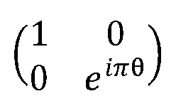
- Phase operations Z ⁇ are single-qubit gates that leave the basis state
- 1 ⁇ , where ⁇ represents a phase shift: Z ⁇ 1 0 0 e i ⁇ .
- 1 ⁇ after application of a phase operation does not change, but the phase of the quantum state is shifted.
- Phase operations are common operations in quantum circuits. Phasing by 180 degrees (Z gates) or 90 degrees (S gates) is relatively straightforward to implement and has low cost. Phasing by 45 degrees (T gates) has increased cost. Furthermore, phasing by angles that are not multiples of 45 degrees is even more costly, since such phase operations typically require approximating the target operation with T gates, and the number of T gates required to obtain a good approximation of a target phase angle increases as the target precision becomes more exact. For example, in some cases performing a non-45-degree phasing operation may require up to 50 T gates.
- This specification describes various techniques for reducing the number of T gates required for performing phase operations Z ⁇ .
- the techniques include using addition operations to merge phasing operations, e.g., performing two T gates using five T gates, duplicating states when performing phase operations, and performing individual T , T or more generally ( T ) 2- n gates with reduced T count.
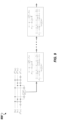
- FIG. 1 depicts an exemplary system 100 for performing phase operations.
- the system 100 is an example of a system implemented as quantum and/or classical computer programs on one or more quantum computing devices and/or classical computers in one or more locations, in which the systems, components, and techniques described below can be implemented.
- the system 100 includes a quantum computing device 102 in data communication with one or more classical processors 104.
- the quantum computing device 102 and classical processors 104 are illustrated as separate entities, however in some implementations the one or more classical processors may be included in quantum computing device 102.
- the quantum computing device 102 includes components for performing quantum computation.
- the quantum computing device 102 includes at least quantum circuitry 106 and control devices 108.
- the quantum circuitry 106 includes components for performing quantum computations, e.g., components for implementing the various quantum circuits and operations described below with reference to FIGS. 2-11 .
- the quantum circuitry may include a quantum system that includes one or more multi-level quantum subsystems, e.g., a register of qubits 114.
- the type of multi-level quantum subsystems that the system 100 utilizes may vary.
- the multi-level quantum subsystems may be superconducting qubits, e.g., Gmon or Xmon qubits. In some cases it may be convenient to include one or more resonators attached to one or more superconducting qubits.
- ion traps In other cases ion traps, photonic devices or superconducting cavities (with which states may be prepared without requiring qubits) may be used. Further examples of realizations of multi-level quantum subsystems include fluxmon qubits, silicon quantum dots or phosphorus impurity qubits.
- Quantum circuits comprising different quantum logic operations, e.g., single qubit gates, two qubit gates, and three qubit gates such as the NOT gates, CNOT gates, multi target CNOT gates, and logical AND operations described below with reference to FIGS. 2-11 , may be constructed using the quantum circuitry 106. Constructed quantum circuits can be operated/implemented using the control devices 108.
- the type of control devices 108 included in the quantum system depend on the type of qubits included in the quantum computing device.
- the control devices 108 may include devices that control the frequencies of qubits included in the quantum circuitry 106, an excitation pulse generator and control lines that couple the qubits to the excitation pulse generator.
- the control devices may then cause the frequency of each qubit to be adjusted towards or away from a quantum gate frequency of an excitation pulse on a corresponding control driveline.
- the control devices 108 may further include measurement devices, e.g., readout resonators. Measurement results obtained via measurement devices may be provided to the classical processors 104 for processing and analyzing.
- the quantum computing device 102 may include one or more quantum state factories, e.g., T factory 112, for producing quantum states that may be consumed by the quantum circuitry when performing quantum computations.
- T factory 112 may produce T states or T states and provide the produced states to the quantum circuitry 106.
- FIG. 2 is a flowchart of an example process 200 for performing a target phase operation Z ⁇ on both a first qubit prepared in a first input state and a second qubit prepared in a second input state using a third qubit prepared in a phased plus state Z ⁇
- the phased plus state specialized to the target angle of the target phase operation can be created using any of multiple existing techniques.
- the process 200 will be described as being performed by a system of one or more classical or quantum computing devices located in one or more locations.
- a quantum computation system e.g., the system 100 of FIG. 1 , appropriately programmed in accordance with this specification, can perform the process 200.
- the system performs a first NOT operation on the third qubit (step 202).
- the system performs a controlled adder operation on the first, second and third qubit, which includes encoding the result of the controlled adder operation in a fourth qubit (step 204).
- computing the controlled adder operation on the first, second and third qubit includes performing a multi target CNOT operation on the first, second and third qubit, where the first qubit acts as a control for the multi target CNOT operation, computing a logical AND operation between the second and third qubit and encoding the result of the logical AND computation in the fourth qubit, and performing a CNOT operation between the first qubit and the fourth qubit, where the first qubit acts as a control for the CNOT operation.
- Example methods for computing and uncomputing logical AND operations are described in detail in " Quantum circuits with reduced T gate count, "WO 2019/050555 .
- Un-computes the controlled adder operation on the first, second and third qubit (step 208).
- Un-computing the controlled adder operation includes performing a CNOT operation on the first qubit and the fourth qubit, where the first qubit acts as a control for the CNOT operation, un-computing the logical AND operation described above with reference to step 204, and performing a multi target CNOT operation on the first, second and third qubit, where the first qubit acts as a control for the multi-target CNOT operation.
- the system performs a CNOT operation between the first qubit and the third qubit, where the first qubit acts as a control for the CNOT operation (step 210).
- the system performs a CNOT operation between the second qubit and the third qubit, where the second qubit acts as a control for the CNOT operation (step 212).
- the system performs a second NOT operation on the third qubit (step 214).
- steps 208-212 may be replaced by the following steps: performing a CNOT operation on the first qubit and the fourth qubit, where the first qubit acts as a control for the CNOT operation, un-computing the logical AND operation between the second and third qubit, performing a CNOT operation on the second qubit and the third qubit, where the second qubit acts as a control for the CNOT operation, and performing a multi target CNOT operation on the first, second and third qubit, where the first qubit acts as a control for the multi target CNOT operation, as shown in the example quantum circuit 300 described below with reference to FIG. 3A .
- the target phase operation has been applied to the first input state and to the second input state.
- the third qubit returns to its initial state - the phased plus state.
- One or more of these output states can then be provided for use in subsequent computations, as described in more detail below.
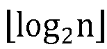
- This concept can be extended to the case of n repeated equiangular rotations appearing in parallel in a circuit: rather than applying the n original arbitrary rotations, the Hamming weight of the relevant qubits can be computed, and instead log 2 n + 1 arbitrary rotations ⁇ , 2 ⁇ , 4 ⁇ , ... can be applied to the Hamming weight. This technique is called Hamming weight phasing.
- Hamming weight phasing can appear to give an improvement for free.
- there are two primary sources of cost - an additional number of T gates and an ancilla qubit requirement, both arising from the use of adder circuits (circuits that include the above described logical AND computations and uncomputations) when computing the Hamming weight.
- adder circuits circuits that include the above described logical AND computations and uncomputations
- the number of required ancilla qubits can be reduced from n - 1 to n + log 2 n or even to 2log 2 n.
- the system can group the n phase operations (or equivalently, n qubits on which the n phase operations are to be performed) into multiple groups of size n and prepare a full-total qubit register of size log 2 n .
- the system computes a Hamming weight of the qubits in the group using n ⁇ 1 ancilla qubits, and adds a computed group-total into the prepared full-total qubit register.
- the system then uncomputes the Hamming weight of the qubits in the group.
- the same n ⁇ 1 ancilla qubits can be used to compute the Hamming weight of each group.
- phase operations can be applied to the total Hamming weight in the full-total register as described above. Then, for each group, the system re-computes the Hamming weight of the qubits in the group and subtracts a computed group total out of the full total register to uncompute the full total Hamming weight register. This reduces the number of ancilla qubits required from n - 1 to n ⁇ 1 to n + log 2 n .
- the number of ancilla qubits is reduced at the cost of requiring more T gates, however the number of T gates required to reduce the original n phase operations to log 2 n + 1 phase operations is approximately upper bounded by 8 n + n log 2 n + 12 log 2 n ⁇ 8 , which is only slightly more than existing applications of Hamming weight phasing methods that require 4n - 4 T gates but significantly more (i.e., n) ancilla qubits.
- n phase operations can also be achieved by dividing the n phase operations into n / log 2 n groups each of size log 2 n. For each of these groups the system can compute the Hamming weight of the qubits in the group, add this weight into an accumulator register full total qubit register), then uncompute the Hamming weight of the qubits in the group. The accumulator register then contains the Hamming weight of the entire set of qubits. Phase operations can be applied to the total Hamming weight in the accumulator register as described above.
- the system performs a reverse of the computation process, e.g., the system re-computes the Hamming weight of the qubits in the group and subtracts a computed group total out of the accumulator register to uncompute the full total Hamming weight register. This doubles the number of addition operations that must be performed, but reduces the space requirements to 2log 2 n.
- FIGS. 3-10 show various applications of example process 200 and Hamming weight phasing.
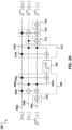
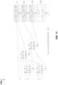
- FIG. 3A is a circuit diagram 300 of an example quantum circuit for performing a target phase operation Z ⁇ on a first and second qubit using a third qubit prepared in a phased plus state Z ⁇
- the first qubit, second qubit and third qubit are represented by horizontal lines 302a-c.
- qubits 302a and 302b represent the first and second qubit on which the target phase operation Z ⁇ is to be performed.
- Qubits 302a and 302b are provided to the example quantum circuit 300 in input states
- ⁇ 1 ⁇ can be initial states of either of the qubits 302a or 302b, i.e., qubits 302a or 302b may have been prepared in arbitrary initial states, or can be states representing an output of a previous computation.
- Qubit 302c represents the third qubit that is prepared in a phased plus state Z ⁇
- the qubit 302c can be prepared in the phased plus state using any one of existing techniques.
- the example quantum circuit 300 includes a sequence of gates that are applied to the qubits 302a-302c.
- the sequence of gates includes a first NOT operation 304 that is applied to the third qubit 302c.
- a first collection of operations 306 are then applied to the qubits 302a-302c to compute a controlled adder operation on the qubits 302a-302c.
- the first collection of operations 306 includes a multi target CNOT gate 306a that is applied to the three qubits 302a-302c, where the first qubit acts as a control for the multi target CNOT gate.
- the first collection of operations 306 further includes a logical AND operation 306b that is performed between the second and third qubit.
- the result of the local AND operation is encoded in a fourth qubit 302d.
- the first collection of operations 306 further includes a CNOT gate 306c that is applied to the first qubit 302a and the fourth qubit 302d, where the first qubit 302a acts as a control for the CNOT gate.
- the sequence of gates further includes a square of the target phase operation 308 that is applied to the fourth qubit 302d.
- a second collection of operations 310 is then applied to the qubits 302a-302d to uncompute the controlled adder operation performed by the first collection of operations 306.
- the second collection of operations 310 includes a CNOT operation 310a that is applied to the first qubit 302a and to the fourth qubit 302d, where the first qubit 302a acts as a control for the CNOT operation 310a.
- the second collection of operations 310 further includes the uncomputation of a logical AND operation 310b between the second qubit 302b and the third qubit 302c.
- the sequence of gates further includes a CNOT operation 312 that is applied to the second qubit 302b and the third qubit 302c, where the second qubit 302b acts as a control for the CNOT operation 312.
- the sequence of gates further includes a multi target CNOT operation 314 that is applied to the first qubit 302a, second qubit 302b and third qubit 302c, where the first qubit 302a acts as a control for the multi target CNOT operation 314.
- the sequence of gates includes a NOT operation 316 that is applied to the third qubit 302c.
- the NOT operation 316 returns the qubit to the original phased plus state Z ⁇
- the target phase operation Z ⁇ has been applied to the first qubit 302a and second qubit 302b. That is, the example quantum circuit 300 operates on a resource state - a
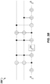
- FIG. 3B is a circuit diagram 350 of an unclaimed example quantum circuit for performing a target phase operation on a first and second qubit using a third qubit prepared in a phased plus state.
- the alterative quantum circuit shown in FIG. 3B produces output states that are the same as those produced by the quantum circuit shown in FIG. 3A , but does not require an ancilla (fourth) qubit. That is, the alternative quantum circuit includes a sequence of gates that are applied to the three qubits 302a-c.
- the sequence of gates includes a NOT operation applied to the third qubit, a multi target CNOT gate that is applied to all three qubits, where the third qubit acts as the control, a CNOT gate that is applied to the third qubit where the first and second qubits act as controls, a square phase operation applied to the third qubit, a CNOT operation that is applied to the third qubit where the first and second qubits act as controls, a multi target CNOT gate that is applied to all three qubits, where the third qubit acts as a control, a CNOT gate applied to the first and third qubit, where the first qubit acts as the control, a CNOT gate applied to the second and third qubit where the second qubit acts as the control, and a NOT operation performed on the third qubit.
- FIG. 4 is a circuit diagram 400 of an example quantum circuit for performing a T gate on a first qubit prepared in a first input state and a second qubit prepared in a second input state using a third qubit prepared in a T + state.
- FIG. 4 shows how two T gates can be performed at a total cost of 5 T gates (four for the adder computations and uncomputations and one for the inner portion of the circuit, e.g., operation 308), or 2.5 T gates per T operation. Since an initial cost of 50 T gates may be required to prepare a T state using existing methods (i.e., methods different to those described in this specification), the presently described techniques are an order of magnitude better than existing techniques in terms of cost.
- the example process 200 described above with reference to FIGS. 2-4 is used to perform an arbitrary target phase operation on both a first qubit prepared in a first input state and a second qubit prepared in a second input state using a third qubit prepared in a phased plus state, where the first input state and second input state can include any arbitrary initial states or states representing an output of a previous computation.
- the techniques described with reference to FIGS. 2-4 can also be utilized to duplicate quantum states while applying target phase operations.
- the second qubit may be prepared in a plus state (i.e., the second input state is a plus state) and the third qubit may be prepared in a phased plus state.
- Application of the example process 200 then maintains the state of the third qubit and duplicates the state of the third qubit by outputting the second qubit in a phased plus state.
- This duplicated state may then be provided for use in a subsequent quantum computation, e.g., as a resource state in a subsequent application of example process 200 for performing a same target phase operation on a fifth and sixth qubit, as a resource state in a subsequent application of example process 200 for duplicating a quantum state while applying a target phase operation, or as a resource state for performing another phase operation, as described below with reference to FIG. 6 .
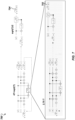
- FIG. 5 is a circuit diagram 500 of an example quantum circuit for duplicating a quantum state while performing a target phase operation Z ⁇ .
- the first qubit, second qubit and third qubit are represented by horizontal lines 502a-c.
- Qubit 502a represents the first qubit on which the target phase operation Z ⁇ is to be performed.
- Qubit 502c represents the third qubit whose state Z ⁇
- qubit 502a is provided to the example quantum circuit in an arbitrary input state
- ⁇ ⁇ can be an initially prepared state of the qubit 502a or can be a state representing an output of a previous computation.
- Qubit 502c is provided to the example quantum circuit in a phased plus state Z ⁇
- qubit 502b is prepared in a plus state
- Operations performed by the example quantum circuit shown in FIG. 5 include a sequence of gates that is similar to that shown and described above with reference to FIG. 3A above. For convenience, a description of this sequence of gates is not repeated.
- the target phase operation Z ⁇ has been applied to the first qubit 502a.
- the target phase operation Z ⁇ has also been applied to the second qubit 502b, which results in a phased plus state Z ⁇
- the quantum state of the third qubit 502c has not been consumed and is also in a phased plus state Z ⁇
- the third qubit in the T + is a resource state and may be reused to perform subsequent gate teleportation operations, e.g., operations based on example process 200.
- the second qubit in the T + state may be used to generate a T ⁇ through application of a subsequent circuit.
- Application of the subsequent circuit may include applying a CNOT operation between the second qubit that is now in a phased plus state and a fifth qubit prepared in an arbitrary input state, where the fifth qubit acts as a control for the CNOT operation.
- the second qubit may then be measured, and a squared phase operation (T operation/gate) may be performed on the fifth qubit if a generated measurement result from measuring the second qubit indicates that the second qubit is ON.
- T operation/gate squared phase operation
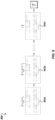
- FIG. 6 is a circuit diagram 600 of an example quantum circuit for performing individual T gates.
- the example quantum circuit shown in FIG. 6 includes two sub-circuits 602 and 604.
- Sub-circuit 604 operates on two qubits - a fifth qubit 606 prepared in an arbitrary input state
- the sub-circuit 604 includes a sequence of gates that may provide a phased input state T ⁇ 614.
- FIG. 7 is a circuit diagram 700 of an example quantum circuit for performing ⁇ T operations.
- both a T state 702 and a ⁇ T state 704 are provided as output from the example quantum circuit.
- ⁇ T states are alternatively produced and consumed when performing lonely ⁇ T operations, and in this case a T inner phasing operation is performed.
- the above described phasing construction requires a second phasing operation with twice the angle of the target phasing operation to be performed.
- the second phasing operation may be performed using the same techniques.
- the second phasing operation may also produce a third phasing operation by four times the angle of the original phasing operation.
- this recursion can be continued as long as desired. (Although in practice, it may be terminated after a number of iterations determined by space-vs-time tradeoffs - more iterations saves more T gates, but more iterations requires more space.)
- FIG. 8 is a circuit diagram of an example quantum circuit ladder construction 800 for iteratively performing ( Z ⁇ ) 2 - n gates until a Z ⁇ gate is performed.
- the example ladder construction 800 is shown as performing a T gate, but this is for convenience only and other phase operations may be performed.
- the phasing operation to be performed delegates to an inner phasing operation, e.g., operation 308 of FIG. 3A and operations 802a-c of FIG. 8 , that phases by twice as much.
- this process can be terminated with a T gate.
- a different approach is needed for angles with odd periods such as 120 degrees, angles that are irrational multiples of 45 degrees such as 1 radian, or angles that are so small that it would be unnecessarily costly to prepare all the necessary resource states reaching from the target angle all the way to the T gate.
- a resource state can be prepared for the desired angle, twice the desired angle, four times the desired angle, etc. up to some finite length.
- this length should scale asymptotically as lg(lg(1/epsilon)).
- the chain may have a length less than 25. The phasing operation is then performed just as it would be for angles that terminate on a T gate, except when "the top of the chain is passed" an operation is applied "the hard way" with existing techniques.
- FIG. 9 shows a first circuit diagram 900 of an example quantum circuit construction for amortizing gate costs over pairs of operations.
- FIG. 10 shows a second circuit diagram 1000 of an example quantum circuit construction for amortizing gate costs over groups of 4 operations.
- Amortizing ladder climbing costs in this manner reduces the maximum average T-count from ⁇ 8 to ⁇ 6 or ⁇ 5 respectively, because the apply-two-phasings-without-consuming-the-resource-state circuit can be used to its full potential, instead of having to alternate it with the circuit that consumes states.
- FIG. 11 shows how interpolating further from iterative application of gates and closer to parallel application of gates causes expected costs to decrease. This is because the raw Hamming weight phasing technique is even more efficient than the iterative ladder based technique.
- Implementations of the digital and/or quantum subject matter and the digital functional operations and quantum operations described in this specification can be implemented in digital electronic circuitry, suitable quantum circuitry or, more generally, quantum computational systems, in tangibly-embodied digital and/or quantum computer software or firmware, in digital and/or quantum computer hardware, including the structures disclosed in this specification and their structural equivalents, or in combinations of one or more of them.
- quantum computational systems may include, but is not limited to, quantum computers, quantum information processing systems, quantum cryptography systems, or quantum simulators.
- Implementations of the digital and/or quantum subject matter described in this specification can be implemented as one or more digital and/or quantum computer programs, i.e., one or more modules of digital and/or quantum computer program instructions encoded on a tangible non-transitory storage medium for execution by, or to control the operation of, data processing apparatus.
- the digital and/or quantum computer storage medium can be a machine-readable storage device, a machine-readable storage substrate, a random or serial access memory device, one or more qubits, or a combination of one or more of them.
- the program instructions can be encoded on an artificially-generated propagated signal that is capable of encoding digital and/or quantum information, e.g., a machine-generated electrical, optical, or electromagnetic signal, that is generated to encode digital and/or quantum information for transmission to suitable receiver apparatus for execution by a data processing apparatus.
- digital and/or quantum information e.g., a machine-generated electrical, optical, or electromagnetic signal
- quantum information and quantum data refer to information or data that is carried by, held or stored in quantum systems, where the smallest non-trivial system is a qubit, i.e., a system that defines the unit of quantum information.
- qubit encompasses all quantum systems that may be suitably approximated as a two-level system in the corresponding context.
- Such quantum systems may include multi-level systems, e.g., with two or more levels.
- such systems can include atoms, electrons, photons, ions or superconducting qubits.
- the computational basis states are identified with the ground and first excited states, however it is understood that other setups where the computational states are identified with higher level excited states are possible.
- data processing apparatus refers to digital and/or quantum data processing hardware and encompasses all kinds of apparatus, devices, and machines for processing digital and/or quantum data, including by way of example a programmable digital processor, a programmable quantum processor, a digital computer, a quantum computer, multiple digital and quantum processors or computers, and combinations thereof.
- the apparatus can also be, or further include, special purpose logic circuitry, e.g., an FPGA (field programmable gate array), an ASIC (application-specific integrated circuit), or a quantum simulator, i.e., a quantum data processing apparatus that is designed to simulate or produce information about a specific quantum system.
- a quantum simulator is a special purpose quantum computer that does not have the capability to perform universal quantum computation.
- the apparatus can optionally include, in addition to hardware, code that creates an execution environment for digital and/or quantum computer programs, e.g., code that constitutes processor firmware, a protocol stack, a database management system, an operating system, or a combination of one or more of them.
- code that creates an execution environment for digital and/or quantum computer programs e.g., code that constitutes processor firmware, a protocol stack, a database management system, an operating system, or a combination of one or more of them.
- a digital computer program which may also be referred to or described as a program, software, a software application, a module, a software module, a script, or code, can be written in any form of programming language, including compiled or interpreted languages, or declarative or procedural languages, and it can be deployed in any form, including as a stand-alone program or as a module, component, subroutine, or other unit suitable for use in a digital computing environment.
- a quantum computer program which may also be referred to or described as a program, software, a software application, a module, a software module, a script, or code, can be written in any form of programming language, including compiled or interpreted languages, or declarative or procedural languages, and translated into a suitable quantum programming language, or can be written in a quantum programming language, e.g., QCL or Quipper.
- a digital and/or quantum computer program may, but need not, correspond to a file in a file system.
- a program can be stored in a portion of a file that holds other programs or data, e.g., one or more scripts stored in a markup language document, in a single file dedicated to the program in question, or in multiple coordinated files, e.g., files that store one or more modules, sub-programs, or portions of code.
- a digital and/or quantum computer program can be deployed to be executed on one digital or one quantum computer or on multiple digital and/or quantum computers that are located at one site or distributed across multiple sites and interconnected by a digital and/or quantum data communication network.
- a quantum data communication network is understood to be a network that may transmit quantum data using quantum systems, e.g. qubits. Generally, a digital data communication network cannot transmit quantum data, however a quantum data communication network may transmit both quantum data and digital data.
- the processes and logic flows described in this specification can be performed by one or more programmable digital and/or quantum computers, operating with one or more digital and/or quantum processors, as appropriate, executing one or more digital and/or quantum computer programs to perform functions by operating on input digital and quantum data and generating output.
- the processes and logic flows can also be performed by, and apparatus can also be implemented as, special purpose logic circuitry, e.g., an FPGA or an ASIC, or a quantum simulator, or by a combination of special purpose logic circuitry or quantum simulators and one or more programmed digital and/or quantum computers.
- a system of one or more digital and/or quantum computers to be "configured to" perform particular operations or actions means that the system has installed on it software, firmware, hardware, or a combination of them that in operation cause the system to perform the operations or actions.
- one or more digital and/or quantum computer programs to be configured to perform particular operations or actions means that the one or more programs include instructions that, when executed by digital and/or quantum data processing apparatus, cause the apparatus to perform the operations or actions.
- a quantum computer may receive instructions from a digital computer that, when executed by the quantum computing apparatus, cause the apparatus to perform the operations or actions.
- Digital and/or quantum computers suitable for the execution of a digital and/or quantum computer program can be based on general or special purpose digital and/or quantum processors or both, or any other kind of central digital and/or quantum processing unit.
- a central digital and/or quantum processing unit will receive instructions and digital and/or quantum data from a read-only memory, a random access memory, or quantum systems suitable for transmitting quantum data, e.g. photons, or combinations thereof.
- the essential elements of a digital and/or quantum computer are a central processing unit for performing or executing instructions and one or more memory devices for storing instructions and digital and/or quantum data.
- the central processing unit and the memory can be supplemented by, or incorporated in, special purpose logic circuitry or quantum simulators.
- a digital and/or quantum computer will also include, or be operatively coupled to receive digital and/or quantum data from or transfer digital and/or quantum data to, or both, one or more mass storage devices for storing digital and/or quantum data, e.g., magnetic, magneto-optical disks, optical disks, or quantum systems suitable for storing quantum information.
- mass storage devices for storing digital and/or quantum data, e.g., magnetic, magneto-optical disks, optical disks, or quantum systems suitable for storing quantum information.
- a digital and/or quantum computer need not have such devices.
- Digital and/or quantum computer-readable media suitable for storing digital and/or quantum computer program instructions and digital and/or quantum data include all forms of non-volatile digital and/or quantum memory, media and memory devices, including by way of example semiconductor memory devices, e.g., EPROM, EEPROM, and flash memory devices; magnetic disks, e.g., internal hard disks or removable disks; magneto-optical disks; CD-ROM and DVD-ROM disks; and quantum systems, e.g., trapped atoms or electrons.
- semiconductor memory devices e.g., EPROM, EEPROM, and flash memory devices
- magnetic disks e.g., internal hard disks or removable disks
- magneto-optical disks CD-ROM and DVD-ROM disks
- quantum systems e.g., trapped atoms or electrons.
- quantum memories are devices that can store quantum data for a long time with high fidelity and efficiency, e.g., light-matter interfaces where light is used for transmission and matter for storing and preserving the quantum features of quantum data such as superposition or quantum coherence.
- Control of the various systems described in this specification, or portions of them, can be implemented in a digital and/or quantum computer program product that includes instructions that are stored on one or more non-transitory machine-readable storage media, and that are executable on one or more digital and/or quantum processing devices.
- the systems described in this specification, or portions of them, can each be implemented as an apparatus, method, or system that may include one or more digital and/or quantum processing devices and memory to store executable instructions to perform the operations described in this specification.
Landscapes
- Engineering & Computer Science (AREA)
- Physics & Mathematics (AREA)
- General Physics & Mathematics (AREA)
- Theoretical Computer Science (AREA)
- Mathematical Physics (AREA)
- General Engineering & Computer Science (AREA)
- Computing Systems (AREA)
- Evolutionary Computation (AREA)
- Mathematical Analysis (AREA)
- Mathematical Optimization (AREA)
- Pure & Applied Mathematics (AREA)
- Data Mining & Analysis (AREA)
- Condensed Matter Physics & Semiconductors (AREA)
- Computational Mathematics (AREA)
- Software Systems (AREA)
- Artificial Intelligence (AREA)
- Computer Hardware Design (AREA)
- Optical Modulation, Optical Deflection, Nonlinear Optics, Optical Demodulation, Optical Logic Elements (AREA)
- Superconductor Devices And Manufacturing Methods Thereof (AREA)
- Compression Or Coding Systems Of Tv Signals (AREA)
- Magnetic Resonance Imaging Apparatus (AREA)
- Compression Of Band Width Or Redundancy In Fax (AREA)
- Circuits Of Receivers In General (AREA)
- Networks Using Active Elements (AREA)
Claims (9)
- Verfahren zum Anwenden einer Zielphase auf ein erstes Qubit einer Quantenrechenvorrichtung und ein zweites Qubit der Quantenrechenvorrichtung durch Durchführen einer Phasenoperation auf dem ersten und zweiten Qubit unter Verwendung eines dritten Qubits der Quantenrechenvorrichtung, das in einem phasengesteuerten Plus-Zustand vorbereitet ist, durchgeführt durch eine Quantenrechenvorrichtung, wobei der phasengesteuerte Plus-Zustand einen Plus-Zustand |+> = (|0 > +|1 >

wobei das Anwenden der Zielphase auf das erste und zweite Qubit Folgendes umfasst:Durchführen einer ersten NOT-Operation (202) auf dem dritten Qubit;Berechnen einer gesteuerten Addieroperation (204) auf dem ersten, zweiten und dritten Qubit, umfassend:Durchführen eines Mehrziel-CNOT auf dem ersten, zweiten und dritten Qubit, wobei das erste Qubit als die Steuerung fungiert;Berechnen einer logischen AND-Operation zwischen dem zweiten und dritten Qubit und Codieren des Ergebnisses der logischen AND-Berechnung in einem vierten Qubit; undDurchführen einer CNOT-Operation zwischen dem ersten Qubit und dem vierten Qubit, wobei das erste Qubit als die Steuerung fungiert;Durchführen eines Quadrats der Phasenoperation (206) auf dem vierten Qubit;Ausrechnen der gesteuerten Addieroperation (208) auf dem ersten, zweiten und dritten Qubit, umfassend:Durchführen einer CNOT-Operation zwischen dem ersten Qubit und dem vierten Qubit, wobei das erste Qubit als die Steuerung fungiert;Ausrechnen einer logischen AND-Operation zwischen dem zweiten und dem dritten Qubit; undDurchführen einer Mehrziel-CNOT-Operation auf dem ersten, zweiten und dritten Qubit, wobei das erste Qubit als die Steuerung fungiert;Durchführen einer CNOT-Operation (210) zwischen dem ersten Qubit und dem dritten Qubit, wobei das erste Qubit als die Steuerung fungiert;Durchführen einer CNOT-Operation (212) zwischen dem zweiten Qubit und dem dritten Qubit, wobei das zweite Qubit als die Steuerung fungiert; undDurchführen einer zweiten NOT-Operation (214) auf dem dritten Qubit. - Verfahren zum Anwenden einer Zielphase auf ein erstes Qubit einer Quantenrechenvorrichtung (302a) und ein zweites Qubit der Quantenrechenvorrichtung (302b) durch Durchführen einer Phasenoperation auf dem ersten und zweiten Qubit unter Verwendung eines dritten Qubits der Quantenrechenvorrichtung (302c), das in einem phasengesteuerten Plus-Zustand vorbereitet ist, durchgeführt durch eine Quantenrechenvorrichtung, wobei der phasengesteuerte Plus-Zustand einen Plus-Zustand |+>= (|0 > +|1 >

wobei das Anwenden der Zielphase auf das erste und zweite Qubit Folgendes umfasst:Durchführen einer ersten NOT-Operation (304) auf dem dritten Qubit;Berechnen einer gesteuerten Addieroperation (306) auf dem ersten, zweiten und dritten Qubit, umfassend:Durchführen eines Mehrziel-CNOT (306a) auf dem ersten, zweiten und dritten Qubit, wobei das erste Qubit als die Steuerung fungiert;Berechnen einer logischen AND-Operation (306b) zwischen dem zweiten und dritten Qubit und Codieren des Ergebnisses der logischen AND-Berechnung in dem vierten Qubit; undDurchführen einer CNOT-Operation (306c) zwischen dem ersten Qubit und dem vierten Qubit, wobei das erste Qubit als die Steuerung fungiert;Durchführen eines Quadrats der Phasenoperation (308) auf dem vierten Qubit;Ausrechnen einer gesteuerten Addieroperation (310) auf dem ersten, zweiten und dritten Qubit, umfassend:
Durchführen einer CNOT-Operation (310a) zwischen dem ersten Qubit und dem vierten Qubit, wobei das erste Qubit als die Steuerung fungiert; undAusrechnen einer logischen AND-Operation (310b) zwischen dem zweiten und dem dritten Qubit;Durchführen einer CNOT-Operation (312) zwischen dem zweiten Qubit und dem dritten Qubit, wobei das zweite Qubit als die Steuerung fungiert;Durchführen einer Mehrziel-CNOT-Operation (314) zwischen dem ersten Qubit, dem zweiten Qubit und dem dritten Qubit, wobei das erste Qubit als die Steuerung fungiert; undDurchführen einer zweiten NOT-Operation (316) auf dem dritten Qubit. - Verfahren nach einem der Ansprüche 1 bis 2, wobei das erste und zweite Qubit initial in beliebigen Ausgangszustand vorbereitet werden.
- Verfahren nach einem der Ansprüche 1 bis 3, wobei:
das erste Qubit in einem beliebigen Ausgangszustand, das zweite Qubit in einem Plus-Zustand und das dritte Qubit in einem phasengleichen Plus-Zustand vorbereitet wird. - Verfahren nach Anspruch 4, ferner umfassend Bereitstellen des zweiten Qubits im phasengesteuerten Plus-Zustand zur Verwendung in einer Operation der Gatterteleportation.
- Verfahren nach einem der vorhergehenden Ansprüche, wobei die Phasenoperation eine einzelne Qubit-Operation der Form Zθ =
- Verfahren nach einem vorhergehenden Anspruch, wobei die Phasenoperation eine Operation

- Verfahren nach einer der Ansprüche 1 oder 2, ferner umfassend, für ein System, das n Anwendungen von Phasenoperationen erfordert, die an n jeweiligen Qubits durchgeführt werden:Gruppieren von Qubits, die eine Phasenoperation erfordern, in

 Vorbereiten eines Gesamtsummen-Qubit-Registers von Größe
 für jede Gruppe:Berechnen eines Hamming-Gewichts der Qubits in der Gruppe;Addieren einer berechneten Gruppensumme in das Gesamtsummenregister;Ausrechnen des Hamming-Gewichts der Qubits in der Gruppe;Durchführen von Phasenoperationen an dem Gesamt-Hamming-Gewicht in dem Gesamtsummenregister;für jede Gruppe:Berechnen eines Hamming-Gewichts der Qubits in der Gruppe;Subtrahieren einer berechneten Gruppensumme aus dem Gesamtsummenregister; undAusrechnen des Hamming-Gewichts der Qubits in der Gruppe,optional ferner umfassend das Löschen und Verwerfen des Gesamtsummenregisters.
 - Gerät (100), umfassend Quantenhardware (102) in Datenkommunikation mit einem oder mehreren klassischen Prozessoren (104), wobei die Quantenhardware Folgendes umfasst:ein Register von Qubits (114), umfassend das erste, zweite, dritte und vierte Qubit nach Anspruch 1;eine Vielzahl von Steuerleitungen, die mit dem Register von Qubits gekoppelt ist;eine Vielzahl von Steuerschaltungen (108), die mit der Vielzahl von Steuerleitungen gekoppelt sind, wobei die Vielzahl von Steuerschaltungen dazu konfiguriert ist, auf dem Register von Qubits das Verfahren eines der Ansprüche 1 bis 8 durchzuführen.
Priority Applications (1)
| Application Number | Priority Date | Filing Date | Title |
|---|---|---|---|
| EP25157671.6A EP4530937A3 (de) | 2018-04-17 | 2019-04-16 | Verfahren und vorrichtung zur durchführung von phasenoperationen |
Applications Claiming Priority (2)
| Application Number | Priority Date | Filing Date | Title |
|---|---|---|---|
| US201862658993P | 2018-04-17 | 2018-04-17 | |
| PCT/US2019/027640 WO2019204282A1 (en) | 2018-04-17 | 2019-04-16 | Methods and apparatus for performing phase operations |
Related Child Applications (2)
| Application Number | Title | Priority Date | Filing Date |
|---|---|---|---|
| EP25157671.6A Division EP4530937A3 (de) | 2018-04-17 | 2019-04-16 | Verfahren und vorrichtung zur durchführung von phasenoperationen |
| EP25157671.6A Division-Into EP4530937A3 (de) | 2018-04-17 | 2019-04-16 | Verfahren und vorrichtung zur durchführung von phasenoperationen |
Publications (2)
| Publication Number | Publication Date |
|---|---|
| EP3586278A1 EP3586278A1 (de) | 2020-01-01 |
| EP3586278B1 true EP3586278B1 (de) | 2025-03-26 |
Family
ID=66380182
Family Applications (2)
| Application Number | Title | Priority Date | Filing Date |
|---|---|---|---|
| EP25157671.6A Pending EP4530937A3 (de) | 2018-04-17 | 2019-04-16 | Verfahren und vorrichtung zur durchführung von phasenoperationen |
| EP19721473.7A Active EP3586278B1 (de) | 2018-04-17 | 2019-04-16 | Verfahren und vorrichtung zur durchführung von phasenoperationen |
Family Applications Before (1)
| Application Number | Title | Priority Date | Filing Date |
|---|---|---|---|
| EP25157671.6A Pending EP4530937A3 (de) | 2018-04-17 | 2019-04-16 | Verfahren und vorrichtung zur durchführung von phasenoperationen |
Country Status (7)
| Country | Link |
|---|---|
| US (3) | US11625637B2 (de) |
| EP (2) | EP4530937A3 (de) |
| JP (2) | JP6930032B2 (de) |
| CN (2) | CN111279368B (de) |
| AU (4) | AU2019255217B2 (de) |
| CA (2) | CA3219315A1 (de) |
| WO (1) | WO2019204282A1 (de) |
Families Citing this family (13)
| Publication number | Priority date | Publication date | Assignee | Title |
|---|---|---|---|---|
| CA3157270A1 (en) * | 2019-11-20 | 2021-05-27 | Pierre-luc DALLAIRE-DEMERS | Quantum algorithm and design for a quantum circuit architecture to simulate interacting fermions |
| US11681939B2 (en) | 2020-04-08 | 2023-06-20 | QC Ware Corp. | Quantum data loader |
| US12277479B2 (en) | 2020-04-08 | 2025-04-15 | QC Ware Corp. | Hardware designs for photonics quantum data loaders |
| US12608635B2 (en) * | 2020-07-24 | 2026-04-21 | Industry-University Cooperation Foundation Hanyang University Erica Campus | Efficient quantum modular multiplier and quantum modular multiplication method |
| JP7651780B2 (ja) * | 2021-10-22 | 2025-03-26 | クオンティニュアム エルエルシー | 任意角度ゲートおよび/またはグローバルゲートを含む量子ゲートセット |
| US12524695B2 (en) | 2021-10-22 | 2026-01-13 | Quantinuum Llc | Quantum gate set including arbitrary angle gates and/or global gates |
| US20240005189A1 (en) * | 2021-11-24 | 2024-01-04 | Qulabz Inc. | Techniques of quantum computing model |
| CN117114118B (zh) * | 2022-05-17 | 2025-10-10 | 本源量子计算科技(合肥)股份有限公司 | 量子权重加和器的构建方法、装置、介质及电子装置 |
| US12579459B2 (en) * | 2022-07-13 | 2026-03-17 | International Business Machines Corporation | Quantum circuit for transformation of mixed state vectors |
| US12561594B2 (en) * | 2022-07-13 | 2026-02-24 | International Business Machines Corporation | Quantum circuits for matrix trace estimation |
| US12505370B2 (en) | 2022-07-13 | 2025-12-23 | International Business Machines Corporation | Linear-depth quantum system for topological data analysis |
| CN116306948B (zh) * | 2022-11-29 | 2024-08-16 | 北京量子信息科学研究院 | 量子信息处理装置及量子信息处理方法 |
| CN119204237B (zh) * | 2023-06-26 | 2025-11-18 | 本源量子计算科技(合肥)股份有限公司 | 一种量子加法器、运算方法及相关装置 |
Family Cites Families (10)
| Publication number | Priority date | Publication date | Assignee | Title |
|---|---|---|---|---|
| US20030164490A1 (en) * | 2001-02-13 | 2003-09-04 | Alexandre Blais | Optimization method for quantum computing process |
| WO2006023082A2 (en) | 2004-07-26 | 2006-03-02 | Hewlett-Packard Development Company, L.P. | Quantum coherent systems and operations |
| CN101118608B (zh) * | 2007-08-23 | 2011-07-20 | 清华大学 | 任意量子比特门的分解方法 |
| US8957699B2 (en) | 2012-10-26 | 2015-02-17 | Northrop Grumman Systems Corporation | Efficient Toffoli state generation from low-fidelity single qubit magic states |
| US9692419B2 (en) * | 2014-11-15 | 2017-06-27 | Wave Computing, Inc. | Compact logic evaluation gates using null convention |
| US10275717B2 (en) | 2016-06-02 | 2019-04-30 | Google Llc | Training quantum evolutions using sublogical controls |
| US10311370B2 (en) * | 2016-08-17 | 2019-06-04 | International Business Machines Corporation | Efficient reduction of resources for the simulation of Fermionic Hamiltonians on quantum hardware |
| CN117808107A (zh) | 2017-09-08 | 2024-04-02 | 谷歌有限责任公司 | 具有减少的t门计数的量子电路 |
| EP3918539B1 (de) * | 2019-03-29 | 2024-11-06 | Google LLC | Oberflächencodeberechnungen unter verwendung von auto-ccz-quantenzuständen |
| WO2022051395A1 (en) * | 2020-09-01 | 2022-03-10 | Google Llc | Verified quantum phase estimation |
-
2019
- 2019-04-16 JP JP2020520504A patent/JP6930032B2/ja active Active
- 2019-04-16 EP EP25157671.6A patent/EP4530937A3/de active Pending
- 2019-04-16 US US16/753,699 patent/US11625637B2/en active Active
- 2019-04-16 WO PCT/US2019/027640 patent/WO2019204282A1/en not_active Ceased
- 2019-04-16 CN CN201980005351.2A patent/CN111279368B/zh active Active
- 2019-04-16 CN CN202311785451.6A patent/CN117910585A/zh active Pending
- 2019-04-16 AU AU2019255217A patent/AU2019255217B2/en active Active
- 2019-04-16 EP EP19721473.7A patent/EP3586278B1/de active Active
- 2019-04-16 CA CA3219315A patent/CA3219315A1/en active Pending
- 2019-04-16 CA CA3080180A patent/CA3080180A1/en active Pending
-
2021
- 2021-02-17 AU AU2021201027A patent/AU2021201027B2/en active Active
- 2021-08-10 JP JP2021130663A patent/JP7227322B2/ja active Active
-
2022
- 2022-02-28 AU AU2022201377A patent/AU2022201377B2/en active Active
-
2023
- 2023-03-09 US US18/181,419 patent/US11941488B2/en active Active
-
2024
- 2024-01-03 AU AU2024200037A patent/AU2024200037A1/en active Pending
- 2024-02-23 US US18/586,154 patent/US12288130B2/en active Active
Non-Patent Citations (2)
| Title |
|---|
| CRAIG GIDNEY: "Proxy Phasing and Computed Phasing", 21 November 2017 (2017-11-21), XP055848275, Retrieved from the Internet <URL:https://algassert.com/post/1719> [retrieved on 20211006] * |
| SERGEI BRAVYI ET AL: "Universal Quantum Computation with ideal Clifford gates and noisy ancillas", ARXIV.ORG, CORNELL UNIVERSITY LIBRARY, 201 OLIN LIBRARY CORNELL UNIVERSITY ITHACA, NY 14853, 3 March 2004 (2004-03-03), XP080147804, DOI: 10.1103/PHYSREVA.71.022316 * |
Also Published As
| Publication number | Publication date |
|---|---|
| US11625637B2 (en) | 2023-04-11 |
| JP7227322B2 (ja) | 2023-02-21 |
| JP2021193570A (ja) | 2021-12-23 |
| AU2022201377B2 (en) | 2023-10-05 |
| US20210027187A1 (en) | 2021-01-28 |
| AU2019255217A1 (en) | 2020-04-16 |
| CA3080180A1 (en) | 2019-10-24 |
| AU2022201377A1 (en) | 2022-03-24 |
| AU2021201027B2 (en) | 2021-12-02 |
| EP4530937A2 (de) | 2025-04-02 |
| US20230297864A1 (en) | 2023-09-21 |
| CN111279368B (zh) | 2024-01-09 |
| JP2021505982A (ja) | 2021-02-18 |
| CN117910585A (zh) | 2024-04-19 |
| US20240232673A1 (en) | 2024-07-11 |
| CN111279368A (zh) | 2020-06-12 |
| WO2019204282A1 (en) | 2019-10-24 |
| EP4530937A3 (de) | 2025-06-25 |
| US12288130B2 (en) | 2025-04-29 |
| US11941488B2 (en) | 2024-03-26 |
| CA3219315A1 (en) | 2019-10-24 |
| JP6930032B2 (ja) | 2021-09-01 |
| AU2024200037A1 (en) | 2024-01-25 |
| EP3586278A1 (de) | 2020-01-01 |
| AU2021201027A1 (en) | 2021-03-11 |
| AU2019255217B2 (en) | 2021-01-14 |
Similar Documents
| Publication | Publication Date | Title |
|---|---|---|
| EP3586278B1 (de) | Verfahren und vorrichtung zur durchführung von phasenoperationen | |
| US11636373B2 (en) | Measurement based uncomputation for quantum circuit optimization | |
| AU2021200999B2 (en) | Quantum circuits with reduced t gate count | |
| US12210502B2 (en) | Performing unitary iteration and indexed operations | |
| US11909392B2 (en) | Magic state factory constructions for producing CCZ and T states | |
| WO2017111937A1 (en) | Triangular dual embedding for quantum annealing | |
| US20240265284A1 (en) | Error corrected variational algorithms |
Legal Events
| Date | Code | Title | Description |
|---|---|---|---|
| STAA | Information on the status of an ep patent application or granted ep patent |
Free format text: STATUS: UNKNOWN |
|
| STAA | Information on the status of an ep patent application or granted ep patent |
Free format text: STATUS: THE INTERNATIONAL PUBLICATION HAS BEEN MADE |
|
| PUAI | Public reference made under article 153(3) epc to a published international application that has entered the european phase |
Free format text: ORIGINAL CODE: 0009012 |
|
| STAA | Information on the status of an ep patent application or granted ep patent |
Free format text: STATUS: REQUEST FOR EXAMINATION WAS MADE |
|
| 17P | Request for examination filed |
Effective date: 20190924 |
|
| AK | Designated contracting states |
Kind code of ref document: A1 Designated state(s): AL AT BE BG CH CY CZ DE DK EE ES FI FR GB GR HR HU IE IS IT LI LT LU LV MC MK MT NL NO PL PT RO RS SE SI SK SM TR |
|
| AX | Request for extension of the european patent |
Extension state: BA ME |
|
| DAV | Request for validation of the european patent (deleted) | ||
| DAX | Request for extension of the european patent (deleted) | ||
| STAA | Information on the status of an ep patent application or granted ep patent |
Free format text: STATUS: EXAMINATION IS IN PROGRESS |
|
| 17Q | First examination report despatched |
Effective date: 20211013 |
|
| REG | Reference to a national code |
Ref country code: DE Ref legal event code: R079 Free format text: PREVIOUS MAIN CLASS: G06N0010000000 Ipc: G06N0010200000 Ref document number: 602019067748 Country of ref document: DE |
|
| GRAP | Despatch of communication of intention to grant a patent |
Free format text: ORIGINAL CODE: EPIDOSNIGR1 |
|
| STAA | Information on the status of an ep patent application or granted ep patent |
Free format text: STATUS: GRANT OF PATENT IS INTENDED |
|
| RIC1 | Information provided on ipc code assigned before grant |
Ipc: G06N 10/20 20220101AFI20241002BHEP |
|
| INTG | Intention to grant announced |
Effective date: 20241015 |
|
| GRAS | Grant fee paid |
Free format text: ORIGINAL CODE: EPIDOSNIGR3 |
|
| GRAA | (expected) grant |
Free format text: ORIGINAL CODE: 0009210 |
|
| STAA | Information on the status of an ep patent application or granted ep patent |
Free format text: STATUS: THE PATENT HAS BEEN GRANTED |
|
| AK | Designated contracting states |
Kind code of ref document: B1 Designated state(s): AL AT BE BG CH CY CZ DE DK EE ES FI FR GB GR HR HU IE IS IT LI LT LU LV MC MK MT NL NO PL PT RO RS SE SI SK SM TR |
|
| P01 | Opt-out of the competence of the unified patent court (upc) registered |
Free format text: CASE NUMBER: APP_7430/2025 Effective date: 20250213 |
|
| REG | Reference to a national code |
Ref country code: GB Ref legal event code: FG4D |
|
| REG | Reference to a national code |
Ref country code: CH Ref legal event code: EP |
|
| REG | Reference to a national code |
Ref country code: DE Ref legal event code: R096 Ref document number: 602019067748 Country of ref document: DE |
|
| REG | Reference to a national code |
Ref country code: IE Ref legal event code: FG4D Ref country code: NL Ref legal event code: FP |
|
| PGFP | Annual fee paid to national office [announced via postgrant information from national office to epo] |
Ref country code: NL Payment date: 20250427 Year of fee payment: 7 |
|
| PG25 | Lapsed in a contracting state [announced via postgrant information from national office to epo] |
Ref country code: RS Free format text: LAPSE BECAUSE OF FAILURE TO SUBMIT A TRANSLATION OF THE DESCRIPTION OR TO PAY THE FEE WITHIN THE PRESCRIBED TIME-LIMIT Effective date: 20250626 |
|
| PG25 | Lapsed in a contracting state [announced via postgrant information from national office to epo] |
Ref country code: FI Free format text: LAPSE BECAUSE OF FAILURE TO SUBMIT A TRANSLATION OF THE DESCRIPTION OR TO PAY THE FEE WITHIN THE PRESCRIBED TIME-LIMIT Effective date: 20250326 |
|
| PGFP | Annual fee paid to national office [announced via postgrant information from national office to epo] |
Ref country code: DE Payment date: 20250429 Year of fee payment: 7 |
|
| PGFP | Annual fee paid to national office [announced via postgrant information from national office to epo] |
Ref country code: GB Payment date: 20250428 Year of fee payment: 7 |
|
| REG | Reference to a national code |
Ref country code: LT Ref legal event code: MG9D |
|
| PG25 | Lapsed in a contracting state [announced via postgrant information from national office to epo] |
Ref country code: NO Free format text: LAPSE BECAUSE OF FAILURE TO SUBMIT A TRANSLATION OF THE DESCRIPTION OR TO PAY THE FEE WITHIN THE PRESCRIBED TIME-LIMIT Effective date: 20250626 |
|
| PG25 | Lapsed in a contracting state [announced via postgrant information from national office to epo] |
Ref country code: HR Free format text: LAPSE BECAUSE OF FAILURE TO SUBMIT A TRANSLATION OF THE DESCRIPTION OR TO PAY THE FEE WITHIN THE PRESCRIBED TIME-LIMIT Effective date: 20250326 |
|
| PG25 | Lapsed in a contracting state [announced via postgrant information from national office to epo] |
Ref country code: LV Free format text: LAPSE BECAUSE OF FAILURE TO SUBMIT A TRANSLATION OF THE DESCRIPTION OR TO PAY THE FEE WITHIN THE PRESCRIBED TIME-LIMIT Effective date: 20250326 |
|
| PGFP | Annual fee paid to national office [announced via postgrant information from national office to epo] |
Ref country code: FR Payment date: 20250425 Year of fee payment: 7 |
|
| PG25 | Lapsed in a contracting state [announced via postgrant information from national office to epo] |
Ref country code: GR Free format text: LAPSE BECAUSE OF FAILURE TO SUBMIT A TRANSLATION OF THE DESCRIPTION OR TO PAY THE FEE WITHIN THE PRESCRIBED TIME-LIMIT Effective date: 20250627 Ref country code: BG Free format text: LAPSE BECAUSE OF FAILURE TO SUBMIT A TRANSLATION OF THE DESCRIPTION OR TO PAY THE FEE WITHIN THE PRESCRIBED TIME-LIMIT Effective date: 20250326 |
|
| PG25 | Lapsed in a contracting state [announced via postgrant information from national office to epo] |
Ref country code: SE Free format text: LAPSE BECAUSE OF FAILURE TO SUBMIT A TRANSLATION OF THE DESCRIPTION OR TO PAY THE FEE WITHIN THE PRESCRIBED TIME-LIMIT Effective date: 20250326 |
|
| REG | Reference to a national code |
Ref country code: AT Ref legal event code: MK05 Ref document number: 1779684 Country of ref document: AT Kind code of ref document: T Effective date: 20250326 |
|
| PG25 | Lapsed in a contracting state [announced via postgrant information from national office to epo] |
Ref country code: SM Free format text: LAPSE BECAUSE OF FAILURE TO SUBMIT A TRANSLATION OF THE DESCRIPTION OR TO PAY THE FEE WITHIN THE PRESCRIBED TIME-LIMIT Effective date: 20250326 |
|
| PG25 | Lapsed in a contracting state [announced via postgrant information from national office to epo] |
Ref country code: ES Free format text: LAPSE BECAUSE OF FAILURE TO SUBMIT A TRANSLATION OF THE DESCRIPTION OR TO PAY THE FEE WITHIN THE PRESCRIBED TIME-LIMIT Effective date: 20250326 Ref country code: PT Free format text: LAPSE BECAUSE OF FAILURE TO SUBMIT A TRANSLATION OF THE DESCRIPTION OR TO PAY THE FEE WITHIN THE PRESCRIBED TIME-LIMIT Effective date: 20250728 |
|
| PG25 | Lapsed in a contracting state [announced via postgrant information from national office to epo] |
Ref country code: PL Free format text: LAPSE BECAUSE OF FAILURE TO SUBMIT A TRANSLATION OF THE DESCRIPTION OR TO PAY THE FEE WITHIN THE PRESCRIBED TIME-LIMIT Effective date: 20250326 Ref country code: IT Free format text: LAPSE BECAUSE OF FAILURE TO SUBMIT A TRANSLATION OF THE DESCRIPTION OR TO PAY THE FEE WITHIN THE PRESCRIBED TIME-LIMIT Effective date: 20250326 |
|
| PG25 | Lapsed in a contracting state [announced via postgrant information from national office to epo] |
Ref country code: AT Free format text: LAPSE BECAUSE OF FAILURE TO SUBMIT A TRANSLATION OF THE DESCRIPTION OR TO PAY THE FEE WITHIN THE PRESCRIBED TIME-LIMIT Effective date: 20250326 |
|
| PG25 | Lapsed in a contracting state [announced via postgrant information from national office to epo] |
Ref country code: EE Free format text: LAPSE BECAUSE OF FAILURE TO SUBMIT A TRANSLATION OF THE DESCRIPTION OR TO PAY THE FEE WITHIN THE PRESCRIBED TIME-LIMIT Effective date: 20250326 |
|
| PG25 | Lapsed in a contracting state [announced via postgrant information from national office to epo] |
Ref country code: RO Free format text: LAPSE BECAUSE OF FAILURE TO SUBMIT A TRANSLATION OF THE DESCRIPTION OR TO PAY THE FEE WITHIN THE PRESCRIBED TIME-LIMIT Effective date: 20250326 |
|
| PG25 | Lapsed in a contracting state [announced via postgrant information from national office to epo] |
Ref country code: SK Free format text: LAPSE BECAUSE OF FAILURE TO SUBMIT A TRANSLATION OF THE DESCRIPTION OR TO PAY THE FEE WITHIN THE PRESCRIBED TIME-LIMIT Effective date: 20250326 |
|
| PG25 | Lapsed in a contracting state [announced via postgrant information from national office to epo] |
Ref country code: IS Free format text: LAPSE BECAUSE OF FAILURE TO SUBMIT A TRANSLATION OF THE DESCRIPTION OR TO PAY THE FEE WITHIN THE PRESCRIBED TIME-LIMIT Effective date: 20250726 |
|
| REG | Reference to a national code |
Ref country code: CH Ref legal event code: H13 Free format text: ST27 STATUS EVENT CODE: U-0-0-H10-H13 (AS PROVIDED BY THE NATIONAL OFFICE) Effective date: 20251125 |
|
| PG25 | Lapsed in a contracting state [announced via postgrant information from national office to epo] |
Ref country code: LU Free format text: LAPSE BECAUSE OF NON-PAYMENT OF DUE FEES Effective date: 20250416 |
|
| PG25 | Lapsed in a contracting state [announced via postgrant information from national office to epo] |
Ref country code: MC Free format text: LAPSE BECAUSE OF FAILURE TO SUBMIT A TRANSLATION OF THE DESCRIPTION OR TO PAY THE FEE WITHIN THE PRESCRIBED TIME-LIMIT Effective date: 20250326 |
|
| REG | Reference to a national code |
Ref country code: BE Ref legal event code: MM Effective date: 20250430 |
|
| REG | Reference to a national code |
Ref country code: DE Ref legal event code: R097 Ref document number: 602019067748 Country of ref document: DE |
|
| PG25 | Lapsed in a contracting state [announced via postgrant information from national office to epo] |
Ref country code: DK Free format text: LAPSE BECAUSE OF FAILURE TO SUBMIT A TRANSLATION OF THE DESCRIPTION OR TO PAY THE FEE WITHIN THE PRESCRIBED TIME-LIMIT Effective date: 20250326 |
|
| PG25 | Lapsed in a contracting state [announced via postgrant information from national office to epo] |
Ref country code: BE Free format text: LAPSE BECAUSE OF NON-PAYMENT OF DUE FEES Effective date: 20250430 |
|
| PG25 | Lapsed in a contracting state [announced via postgrant information from national office to epo] |
Ref country code: CH Free format text: LAPSE BECAUSE OF NON-PAYMENT OF DUE FEES Effective date: 20250430 |
|
| PG25 | Lapsed in a contracting state [announced via postgrant information from national office to epo] |
Ref country code: CZ Free format text: LAPSE BECAUSE OF FAILURE TO SUBMIT A TRANSLATION OF THE DESCRIPTION OR TO PAY THE FEE WITHIN THE PRESCRIBED TIME-LIMIT Effective date: 20250326 |
|
| PLBE | No opposition filed within time limit |
Free format text: ORIGINAL CODE: 0009261 |
|
| STAA | Information on the status of an ep patent application or granted ep patent |
Free format text: STATUS: NO OPPOSITION FILED WITHIN TIME LIMIT |
|
| REG | Reference to a national code |
Ref country code: CH Ref legal event code: L10 Free format text: ST27 STATUS EVENT CODE: U-0-0-L10-L00 (AS PROVIDED BY THE NATIONAL OFFICE) Effective date: 20260211 |
|
| 26N | No opposition filed |
Effective date: 20260105 |
|
| PG25 | Lapsed in a contracting state [announced via postgrant information from national office to epo] |
Ref country code: IE Free format text: LAPSE BECAUSE OF NON-PAYMENT OF DUE FEES Effective date: 20250416 |