EP3918539B1 - Oberflächencodeberechnungen unter verwendung von auto-ccz-quantenzuständen - Google Patents
Oberflächencodeberechnungen unter verwendung von auto-ccz-quantenzuständen Download PDFInfo
- Publication number
- EP3918539B1 EP3918539B1 EP20721040.2A EP20721040A EP3918539B1 EP 3918539 B1 EP3918539 B1 EP 3918539B1 EP 20721040 A EP20721040 A EP 20721040A EP 3918539 B1 EP3918539 B1 EP 3918539B1
- Authority
- EP
- European Patent Office
- Prior art keywords
- qubit
- routing
- controlled
- classical bit
- classical
- Prior art date
- Legal status (The legal status is an assumption and is not a legal conclusion. Google has not performed a legal analysis and makes no representation as to the accuracy of the status listed.)
- Active
Links
Images


Classifications
-
- G—PHYSICS
- G06—COMPUTING OR CALCULATING; COUNTING
- G06F—ELECTRIC DIGITAL DATA PROCESSING
- G06F9/00—Arrangements for program control, e.g. control units
- G06F9/06—Arrangements for program control, e.g. control units using stored programs, i.e. using an internal store of processing equipment to receive or retain programs
- G06F9/30—Arrangements for executing machine instructions, e.g. instruction decode
- G06F9/30003—Arrangements for executing specific machine instructions
- G06F9/30007—Arrangements for executing specific machine instructions to perform operations on data operands
-
- G—PHYSICS
- G06—COMPUTING OR CALCULATING; COUNTING
- G06F—ELECTRIC DIGITAL DATA PROCESSING
- G06F17/00—Digital computing or data processing equipment or methods, specially adapted for specific functions
- G06F17/10—Complex mathematical operations
-
- G—PHYSICS
- G06—COMPUTING OR CALCULATING; COUNTING
- G06F—ELECTRIC DIGITAL DATA PROCESSING
- G06F7/00—Methods or arrangements for processing data by operating upon the order or content of the data handled
- G06F7/38—Methods or arrangements for performing computations using exclusively denominational number representation, e.g. using binary, ternary, decimal representation
- G06F7/48—Methods or arrangements for performing computations using exclusively denominational number representation, e.g. using binary, ternary, decimal representation using non-contact-making devices, e.g. tube, solid state device; using unspecified devices
- G06F7/4824—Methods or arrangements for performing computations using exclusively denominational number representation, e.g. using binary, ternary, decimal representation using non-contact-making devices, e.g. tube, solid state device; using unspecified devices using signed-digit representation
-
- G—PHYSICS
- G06—COMPUTING OR CALCULATING; COUNTING
- G06F—ELECTRIC DIGITAL DATA PROCESSING
- G06F7/00—Methods or arrangements for processing data by operating upon the order or content of the data handled
- G06F7/38—Methods or arrangements for performing computations using exclusively denominational number representation, e.g. using binary, ternary, decimal representation
- G06F7/48—Methods or arrangements for performing computations using exclusively denominational number representation, e.g. using binary, ternary, decimal representation using non-contact-making devices, e.g. tube, solid state device; using unspecified devices
- G06F7/50—Adding; Subtracting
- G06F7/505—Adding; Subtracting in bit-parallel fashion, i.e. having a different digit-handling circuit for each denomination
- G06F7/5057—Adding; Subtracting in bit-parallel fashion, i.e. having a different digit-handling circuit for each denomination using table look-up; using programmable logic arrays
-
- G—PHYSICS
- G06—COMPUTING OR CALCULATING; COUNTING
- G06F—ELECTRIC DIGITAL DATA PROCESSING
- G06F7/00—Methods or arrangements for processing data by operating upon the order or content of the data handled
- G06F7/60—Methods or arrangements for performing computations using a digital non-denominational number representation, i.e. number representation without radix; Computing devices using combinations of denominational and non-denominational quantity representations, e.g. using difunction pulse trains, STEELE computers, phase computers
- G06F7/72—Methods or arrangements for performing computations using a digital non-denominational number representation, i.e. number representation without radix; Computing devices using combinations of denominational and non-denominational quantity representations, e.g. using difunction pulse trains, STEELE computers, phase computers using residue arithmetic
-
- G—PHYSICS
- G06—COMPUTING OR CALCULATING; COUNTING
- G06F—ELECTRIC DIGITAL DATA PROCESSING
- G06F9/00—Arrangements for program control, e.g. control units
- G06F9/06—Arrangements for program control, e.g. control units using stored programs, i.e. using an internal store of processing equipment to receive or retain programs
- G06F9/30—Arrangements for executing machine instructions, e.g. instruction decode
- G06F9/30003—Arrangements for executing specific machine instructions
- G06F9/30076—Arrangements for executing specific machine instructions to perform miscellaneous control operations, e.g. NOP
-
- G—PHYSICS
- G06—COMPUTING OR CALCULATING; COUNTING
- G06N—COMPUTING ARRANGEMENTS BASED ON SPECIFIC COMPUTATIONAL MODELS
- G06N10/00—Quantum computing, i.e. information processing based on quantum-mechanical phenomena
-
- G—PHYSICS
- G06—COMPUTING OR CALCULATING; COUNTING
- G06N—COMPUTING ARRANGEMENTS BASED ON SPECIFIC COMPUTATIONAL MODELS
- G06N10/00—Quantum computing, i.e. information processing based on quantum-mechanical phenomena
- G06N10/20—Models of quantum computing, e.g. quantum circuits or universal quantum computers
-
- G—PHYSICS
- G06—COMPUTING OR CALCULATING; COUNTING
- G06N—COMPUTING ARRANGEMENTS BASED ON SPECIFIC COMPUTATIONAL MODELS
- G06N10/00—Quantum computing, i.e. information processing based on quantum-mechanical phenomena
- G06N10/40—Physical realisations or architectures of quantum processors or components for manipulating qubits, e.g. qubit coupling or qubit control
-
- G—PHYSICS
- G06—COMPUTING OR CALCULATING; COUNTING
- G06N—COMPUTING ARRANGEMENTS BASED ON SPECIFIC COMPUTATIONAL MODELS
- G06N10/00—Quantum computing, i.e. information processing based on quantum-mechanical phenomena
- G06N10/60—Quantum algorithms, e.g. based on quantum optimisation, quantum Fourier or Hadamard transforms
-
- G—PHYSICS
- G06—COMPUTING OR CALCULATING; COUNTING
- G06N—COMPUTING ARRANGEMENTS BASED ON SPECIFIC COMPUTATIONAL MODELS
- G06N10/00—Quantum computing, i.e. information processing based on quantum-mechanical phenomena
- G06N10/70—Quantum error correction, detection or prevention, e.g. surface codes or magic state distillation
-
- G—PHYSICS
- G11—INFORMATION STORAGE
- G11C—STATIC STORES
- G11C11/00—Digital stores characterised by the use of particular electric or magnetic storage elements; Storage elements therefor
- G11C11/21—Digital stores characterised by the use of particular electric or magnetic storage elements; Storage elements therefor using electric elements
- G11C11/34—Digital stores characterised by the use of particular electric or magnetic storage elements; Storage elements therefor using electric elements using semiconductor devices
- G11C11/40—Digital stores characterised by the use of particular electric or magnetic storage elements; Storage elements therefor using electric elements using semiconductor devices using transistors
- G11C11/401—Digital stores characterised by the use of particular electric or magnetic storage elements; Storage elements therefor using electric elements using semiconductor devices using transistors forming cells needing refreshing or charge regeneration, i.e. dynamic cells
- G11C11/4063—Auxiliary circuits, e.g. for addressing, decoding, driving, writing, sensing or timing
-
- H—ELECTRICITY
- H04—ELECTRIC COMMUNICATION TECHNIQUE
- H04B—TRANSMISSION
- H04B10/00—Transmission systems employing electromagnetic waves other than radio-waves, e.g. infrared, visible or ultraviolet light, or employing corpuscular radiation, e.g. quantum communication
- H04B10/70—Photonic quantum communication
Definitions
- This specification relates to quantum computing.
- Quantum computers have memories made up of bits, where each bit can represent either a zero or a one.
- Quantum computers maintain sequences of quantum bits, called qubits, where each quantum bit can represent a zero, one or any quantum superposition of zeros and ones.
- Quantum computers operate by setting qubits in an initial state and controlling the qubits, e.g., according to a sequence of quantum logic gates.
- Composite Toffoli gate with two-round error detection (C. Jones, Phys. Rev. A 87, 052334, 2013 ) discloses a fault-tolerant construction to implement a composite quantum operation of four overlapping Toffoli gates. The same construction can produce two independent Toffoli gates.
- Performing error corrected quantum computations involves implementing sequences of unitary operations and measurements, where intermediate measurement results are used to determine future unitary operations. For example, in the surface code, performing logical T and T ⁇ gates involves a measurement dependent future S gate.
- the measurement depth of a quantum circuit determines how many times a classical control system will: perform a set of measurements, decide which basis to use for the next set of measurements, and start those measurements.
- the characteristic time taken for the classical control system to react to a measurement and perform a following dependent measurement is referred as the control system's "reaction time”.
- a quantum computation whose speed is limited by the measurement depth of the circuit and the reaction time of the classical control system is referred to as a "reaction limited computation".
- This specification describes techniques for decreasing the space overhead of reaction limited computations and improving qubit routing in reaction limited computations.
- the techniques include: an optimized reaction limited selective CZ operation, referred to herein as a delayed choice CZ, techniques for producing and consuming AutoCCZ states, which make routing easier because they decouple the consumption of the CCZ state from the fixup operations needed to complete a gate teleportation, an improved CCZ distillation factory, and apparatus for performing addition operations and lookup operations.
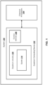
- FIG. 1 depicts an example quantum computation system 100.
- the system 100 is an example of a system implemented as quantum and classical computer programs on one or more quantum computing devices and classical computers in one or more locations, in which the systems, components, and techniques described below can be implemented.
- the system 100 includes a quantum computing device 102 in data communication with one or more classical processors 104.
- the quantum computing device 102 and classical processors 104 are illustrated as separate entities, however in some implementations the classical processors 104 may be included in the quantum computing device 102.
- the quantum computing device 102 includes components for performing quantum computation.
- the quantum computing device 102 includes quantum circuitry 106 and control devices 108.
- the quantum circuitry 106 includes components for performing quantum computations, e.g., components for implementing the various quantum circuits and operations described in this specification.
- the quantum circuitry may include a quantum system that includes one or more multi-level quantum subsystems, e.g., qubits 114.
- the qubits 114 are physical qubits that may be used to perform algorithmic operations or quantum computations.
- the specific realization of the one or more qubits and their interactions may depend on a variety of factors including the type of quantum computations that the quantum computing device 102 is performing.
- the qubits may include qubits that are realized via atomic, molecular or solid-state quantum systems.
- the qubits may include, but are not limited to, superconducting qubits, e.g., Gmon or Xmon qubits, or semi-conducting qubits.
- Further examples of realizations of multi-level quantum subsystems include fluxmon qubits, silicon quantum dots or phosphorus impurity qubits.
- to the quantum circuitry may further include one or more resonators attached to one or more superconducting qubits.
- ion traps, photonic devices or superconducting cavities (with which states may be prepared without requiring qubits) may be used.
- quantum circuit is used to refer to a sequence of quantum logic operations that can be applied to a qubit register to perform a respective computation.
- Quantum circuits comprising different quantum logic operations, e.g., single qubit gates, multi-qubit gates, etc., may be constructed using the quantum circuitry 106. Constructed quantum circuits can be operated/implemented using the control devices 108.
- control devices 108 included in the quantum system depend on the type of qubits included in the quantum computing device.
- the multiple qubits can be frequency tunable. That is, each qubit may have associated operating frequencies that can be adjusted using one or more control devices.
- Example operating frequencies include qubit idling frequencies, qubit interaction frequencies, and qubit readout frequencies. Different frequencies correspond to different operations that the qubit can perform. For example, setting the operating frequency to a corresponding idling frequency may put the qubit into a state where it does not strongly interact with other qubits, and where it may be used to perform single-qubit gates.
- control devices 108 may include devices that control the frequencies of qubits included in the quantum circuitry 106, an excitation pulse generator and control lines that couple the qubits to the excitation pulse generator. The control devices may then cause the frequency of each qubit to be adjusted towards or away from a quantum gate frequency of an excitation pulse on a corresponding control driveline.
- the control devices 108 may further include measurement devices, e.g., readout resonators. Measurement results obtained via measurement devices may be provided to the classical processors 104 for processing and analyzing. Measurement devices perform physical measurements on properties of the qubits, either directly or indirectly, from which the state(s) of the qubits can be inferred. Measurement devices perform physical measurements on properties of the qubits, either directly or indirectly, from which the state(s) of the qubits can be inferred.
- the quantum computing device 102 can further include one or more quantum state factories, e.g., T factories, that produce and store quantum states, e.g., T or CCZ states, to be used in computations performed by the system 100.
- quantum state factories e.g., T factories
- quantum states e.g., T or CCZ states
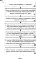
- FIG. 2 is a flow diagram of an example process 200 for performing a delayed choice CZ operation on a first data qubit and a second data qubit.
- the process 200 will be described as being performed by a system of one or more classical and quantum computing devices located in one or more locations.
- a quantum computation system e.g., the system 100 of FIG. 1 , appropriately programmed in accordance with this specification, can perform the process 200.
- the system prepares a first routing qubit and a second routing qubit in a magic state (step 202). For example, the system may prepare the first routing qubit in a plus state, prepare the second routing qubit in a plus state, and perform a CZ operation on the first routing qubit and the second routing qubit.
- the system interacts i) the first data qubit with the first routing qubit, and ii) the second data qubit with the second routing qubit using a first CNOT operation and a second CNOT operation, respectively (step 204).
- the first data qubit and second data qubit act as a first control and a second control for the first CNOT operation and the second CNOT operation, respectively.
- the system stores the states of the first routing qubit and second routing qubit.
- the system receives a first classical bit from a classical processor.
- the first classical bit may be an output of a classical computation that determines whether or not a classical controlled Z operation is to be performed on the first data qubit and second data qubit.
- the system determines whether the first classical bit represents an off state or an on state (step 206).
- the system determines whether the first classical bit represents the off state or on state by determining whether the first classical bit is 0 (where the first classical bit represents an on state) or 1 (where the first classical bit represents an off state).
- the system In response to determining that the first classical bit represents an on state at step 206, the system performs the below described steps 208-212.
- the system applies a first Hadamard gate to the first routing qubit and applies a second Hadamard gate to the second routing qubit (step 208).
- the system measures the first routing qubit using a Z basis measurement to obtain a second classical bit and measures the second routing qubit using a Z basis measurement to obtain a third classical bit (step 210).
- the system performs classically controlled fix up operations on the first data qubit and second data qubit using the second classical bit and the third classical bit (step 212).
- the system applies a classically controlled swap operation to the second classical bit and third classical bit, where the first classical bit acts as a control for the classically controlled swap operation, applies a first classically controlled Z operation to the second data qubit, where the third classical bit acts as a control for the first classically controlled Z operation, and applies a second classically controlled Z operation to the first data qubit, where the second classical bit acts as a control for the second classically controlled Z operation.
- the system In response to determining that the first classical bit represents an off state at step 206, the system performs the below described steps 214-218.
- the system measures the first routing qubit using a Z basis measurement to obtain a fourth classical bit (step 214).
- the system measures the second routing qubit using a Z basis measurement to obtain a fifth classical bit (step 214).
- the system performs classically controlled fix up operations on the first data qubit and second data qubit using the obtained fourth classical bit and fifth classical bit (step 216).
- the system applies a classically controlled swap operation to the fourth classical bit and fifth classical bit, where the first classical bit acts as a control for the classically controlled swap operation, applies a first classically controlled Z operation to the second data qubit, where the fifth classical bit acts as a control for the first classically controlled Z operation, and applies a second classically controlled Z operation to the first data qubit, where the fourth classical bit acts as a control for the second classically controlled Z operation.
- FIG. 3 is a circuit diagram of an example quantum circuit 300 for performing a delayed choice CZ operation 308 on a first data qubit 304 and a second data qubit 306, as shown in box 302.
- the example quantum circuit 300 includes a CZ operation 310 applied to a first routing qubit 312 and a second routing qubit 314, where both the first routing qubit 312 and the second routing qubit 314 are prepared in a plus state.
- Operation 310 corresponds to step 202 of example process 200.
- the example quantum circuit 300 further includes a first CNOT operation 316a and a second CNOT operation 316b.
- the first CNOT operation 316a targets the first routing qubit and uses the first data qubit 304 as a control.
- the second CNOT operation 316b targets the second routing qubit and uses the second data qubit 306 as a control.
- Operations 316a, 316b correspond to step 204 of example process 200.
- the example quantum circuit 300 further includes a first Hadamard gate 318a applied to the first routing qubit 312 and a second Hadamard gate 318b applied to the second routing qubit 314.
- Hadamard gates 318a and 318b are only applied when a classical bit 320 represents an on state (i.e., when the classical bit is a 0).
- Operations 318a, 318b correspond to steps 206-212 of example process 200.
- the example quantum circuit 300 further includes a first measurement operation 322a applied to the first routing qubit 312 and a second measurement operation 322b applied to the second routing qubit 314. Operations 322a, 322b correspond to step 214 of example process 200.
- the example quantum circuit 300 includes a classically controlled swap operation 324 that swaps the output of the measurement operations 322a, 322b if the classical bit 320 represents an on state (i.e., when the classical bit 320 is a 1).
- the example quantum circuit 300 further includes a first classically controlled Z gate 326 that is applied to the first data qubit 304 if an output of the classically controlled swap operation 324 corresponding to the first routing qubit represents an on state.
- the example quantum circuit 300 further includes a second classically controlled Z gate 328 that is applied to the second data qubit 306 if an output of the classically controlled swap operation 324 corresponding to the second routing qubit represents an on state.
- Operations 324-328 correspond to step 216 of example process 200.
- Three instances of the construction for performing delayed choice CZ operations as described in example process 200 of FIG. 2 can be embedded directly into a CCZ state, so that there is one delayed choice CZ for each CZ fixup that may be needed when performing gate teleportation.
- FIG. 4 is a flow diagram of an example process 400 for performing an auto corrected CCZ operation on a first, second and third data qubit.
- the process 200 will be described as being performed by a system of one or more classical and quantum computing devices located in one or more locations.
- a quantum computation system e.g., the system 100 of FIG. 1 , appropriately programmed in accordance with this specification, can perform the process 400.
- the system prepares nine routing qubits in a magic state (step 402). For example, the system may prepare each of the nine routing qubits in a plus state, perform a CCZ operation on the first, fourth and seventh routing qubits, and perform CZ operations on pairs of neighboring routing qubits.
- the system interacts i) the first data qubit with a first routing qubit using a first CNOT operation, ii) the second data qubit with a fourth routing qubit using a second CNOT operation, and iii) the third data qubit with a seventh routing qubit using a third CNOT operation (step 404).
- the first data qubit acts as a control for the first CNOT operation
- the second data qubit acts as a control for the second CNOT operation
- the third data qubit acts as a control for the third CNOT operation.
- the system measures the first, fourth and seventh routing qubits to obtain a first, fourth and seventh classical bit (step 406).
- the system stores the second routing qubit, third routing qubit, fifth routing qubit, sixth routing qubit, eighth routing qubit and ninth routing qubit.
- the system determines whether the first classical bit represents an off state or an on state. In response to determining that the first classical bit represents an on state, the system applies a first Hadamard gate to the fifth routing qubit and applies a second Hadamard gate to the sixth routing qubit (step 408). The system measures the fifth routing qubit using a Z basis measurement to obtain a fifth classical bit and measures the sixth routing qubit using a Z basis measurement to obtain a sixth classical bit (step 410). In response to determining that the first classical bit represents an off state, the system does not perform the first Hadmard gate or second Hadamard gate and directly performs step 410.
- the system determines whether the fourth classical bit represents an off state or an on state. In response to determining that the fourth classical bit represents an on state, the system applies a third Hadamard gate to the eighth routing qubit and applies a fourth Hadamard gate to the ninth routing qubit (step 412). The system measures the eighth routing qubit using a Z basis measurement to obtain a eighth classical bit and measures the ninth routing qubit using a Z basis measurement to obtain a ninth classical bit (step 414). In response to determining that the fourth classical bit represents an off state, the system does not apply the third and fourth Hadamard gates and directly performs step 414.
- the system determines whether the seventh classical bit represents an off state or an on state. In response to determining that the seventh classical bit represents an on state, the system applies a fifth Hadamard gate to the second routing qubit and applies a sixth Hadamard gate to the third routing qubit (step 416). The system measures the second routing qubit using a Z basis measurement to obtain a second classical bit and measures the third routing qubit using a Z basis measurement to obtain a third classical bit (step 418). In response to determining that the seventh classical bit represents an off state, the system does not apply the fifth and sixth Hadamard gates and directly performs step 418.
- the system performs classically controlled fix up operations on the first, second and third data qubits using respective classical bits (step 420).
- the system may: apply a first classically controlled swap operation to the second classical bit and third classical bit, where the seventh classical bit acts as a control for the first classically controlled swap operation, apply a second classically controlled swap operation to the fifth classical bit and sixth classical bit, where the first classical bit acts as a control for the second classically controlled swap operation, apply a third classically controlled swap operation to the eighth classical bit and ninth classical bit, where the fourth classical bit acts as a control for the third classically controlled swap operation, apply multiple classically controlled Z operations to the first, second, and third data qubits, where each classically controlled Z operation uses one of the second, third, fifth, sixth, eighth or ninth classical bits as a control for the classically controlled Z operation, and apply multiple classically controlled-controlled Z operations to the first, second and third data qubits, where each classically controlled-controlled Z operation uses two of the first, fourth and seventh classical bits as controls for the classically
- Applying multiple classically controlled Z operations to the first, second, and third data qubits, wherein each classically controlled Z operation uses one of the second, third, fifth, sixth, eighth or ninth classical bits as a control for the classically controlled Z operation can include: applying a first classically controlled Z operation to the third data qubit, wherein the second classical bit acts as a control for the first classically controlled Z operation; applying a second classically controlled Z operation to the second data qubit, wherein the third classical bit acts as a control for the second classically controlled Z operation; applying a third classically controlled Z operation to the third data qubit, wherein the fifth classical bit acts as the control for the third classically controlled Z operation; applying a fourth classically controlled Z operation to the first data qubit, wherein the sixth classical bit acts as the control for the fourth classically controlled Z operation; applying a fifth classically controlled Z operation to the second data qubit, wherein the eighth classical bit acts as the control for the fifth classically controlled Z operation; and applying a sixth classically controlled Z operation to the first data qubit,
- Applying multiple classically controlled-controlled Z operations to the first, second and third data qubits, wherein each classically controlled-controlled Z operation uses two of the first, fourth and seventh classical bits as controls for the classically controlled-controlled Z operation can include: applying a first classically controlled-controlled Z operation to the first data qubit, wherein the first classical bit and fourth classical bit act as controls for the first classically controlled-controlled Z operation; applying a second classically controlled-controlled Z operation to the second data qubit, wherein the fourth classical bit and seventh classical bit act as controls for the second classically controlled-controlled Z operation; and applying a third classically controlled-controlled Z operation to the third data qubit, wherein the first classical bit and seventh classical bit act as controls for the third classically controlled-controlled Z operation.
- FIG. 5 is a circuit diagram of an example quantum circuit 500 for performing an auto corrected CCZ operation 502 on a first data qubit 504, second data qubit 506 and a third data qubit 508.
- the example quantum circuit 500 includes a CCZ operation 512 applied to a first, fourth and seventh routing qubit in a register 510 that includes nine routing qubits, where each routing qubit is prepared in a plus state.
- the example quantum circuit 500 further includes multiple CZ operations, e.g., CZ operation 514, applied to pairs of neighboring routing qubits (with the convention that the last routing qubit neighbors the first routing qubit).
- the example quantum circuit 300 includes a first CZ operation applied to the first and second routing qubits, a second CZ operation applied to the second and third routing qubits, etc.
- the example quantum circuit 500 includes nine CZ operations.
- the CCZ operation 512 and multiple CZ operation, e.g., CZ operation 514, correspond to step 402 of example process 400.
- the example quantum circuit 500 includes three CNOT operations, e.g., CNOT operation 516.
- a first CNOT operation targets the first routing qubit and uses the first data qubit as a control.
- a second CNOT operation targets the fourth routing qubit and uses the second data qubit as a control.
- a third CNOT operation targets the seventh routing qubit and uses the third data qubit as a control.
- the three CNOT operations correspond to step 404 of example process 400.
- the example quantum circuit 500 includes three measurement operations, e.g., measurement operation 518.
- a first measurement operation measures the first routing qubit.
- a second measurement operation measures the fourth routing qubit.
- a third measurement operation measures the seventh routing qubit.
- the three measurement operations correspond to step 406 of example process 400.
- the example quantum circuit 500 includes multiple Hadamard gates, e.g., Hadamard gate 520.
- a first Hadamard gate and a second Hadamard gate are applied to the second routing qubit and third routing qubit, respectively, if a measurement result of the measurement operation performed on the seventh routing qubit represents an on state.
- a third Hadamard gate and a fourth Hadamard gate are applied to the fifth routing qubit and sixth routing qubit, respectively, if a measurement result of the measurement operation performed on the first routing qubit represents an on state.
- a fifth Hadamard gate and a sixth Hadamard gate are applied to the eighth routing qubit and ninth routing qubit, respectively, if a measurement result of the measurement operation performed on the fourth routing qubit represents an on state.
- the example quantum circuit 500 includes multiple measurement operations, e.g., measurement operation 522, that are applied to the second, third, fifth, sixth, eighth and ninth routing qubits.
- the Hadamard gates and measurement operations described correspond to steps 410-426 of example process 400.
- the example quantum circuit 500 includes multiple classically controlled swap operations, e.g., classically controlled swap operation 524, that swap outputs of respective measurement operations if a respective classical bit represents an on state.
- classically controlled swap operation 524 swaps the outputs of the measurement operations performed on the eighth and ninth routing qubits if the output of the measurement operation performed on the fourth routing qubit represents an on state.
- a second classically controlled swap operation swaps the outputs of the measurement operations performed on the fifth and sixth routing qubits if the output of the measurement operation performed on the first routing qubit represents an on state.
- a third classically controlled swap operation swaps the outputs of the measurement operations performed on the second and third routing qubits if the output of the measurement operation performed on the seventh routing qubit represents an on state.
- the classically control swap operations described correspond to step 428 of example process 400.
- the example quantum circuit 500 includes multiple classically controlled Z gates, e.g., classically controlled Z gate 526, that are applied to the first data qubit 504, second data qubit 506 and third data qubit 508 based on outputs of the three classically controlled swap operations.
- a first Z gate is applied to the first data qubit 504 if an output of the third classically controlled swap operation corresponding to the second routing qubit represents an on state.
- a second Z gate is applied to the second data qubit 506 if an output of the third classically controlled swap operation corresponding to the third routing qubit represents an on state.
- a third Z gate 526 is applied to the second data qubit 506 if an output of the second classically controlled swap operation corresponding to the fifth routing qubit represents an on state.
- a fourth Z gate is applied to the third data qubit 508 if an output of the second classically controlled swap operation corresponding to the sixth routing qubit represents an on state.
- a fifth Z gate is applied to the third data qubit 508 if an output of the first classically controlled swap operation 524 corresponding to the eighth routing qubit represents an on state.
- a sixth Z gate is applied to the first data qubit 504 if an output of the first classically controlled swap operation 524 corresponding to the ninth routing qubit represents an on state.
- a seventh Z gate is applied to the third data qubit if the output of the measurement of the first routing qubit and the fourth routing qubit both represent on states.
- An eighth Z gate is applied to the first data qubit if the output of the measurement of the seventh routing qubit and the fourth routing qubit both represent on states.
- a ninth Z gate is applied to the second data qubit if the output of the measurement of the first routing qubit and the seventh routing qubit both represent on states.
- the multiple classically controlled Z gates correspond to step 428 of example process 400.
- a particularly useful magic state is the CCZ state
- CCZ ⁇ CCZ
- + ⁇ ⁇ 3 ⁇ a , b , c ⁇ 0,1 ⁇ 1 abc
- This quantum state is particularly useful because the quantum equivalent of the AND gate - the Toffoli gate - is not native to the surface code but can be performed by consuming one CCZ state.
- FIG. 6 is a flow diagram of an example process 600 for producing a CCZ quantum state.
- the process 600 will be described as being performed by a system of one or more classical and quantum computing devices located in one or more locations.
- a quantum computation system e.g., the system 100 of FIG. 1 , appropriately programmed in accordance with this specification, can perform the process 600.
- the system obtains a first number of T states of a first quality (step 602).
- the system can obtain the first number of T states from a level-0 T state factory.
- the system can perform state injection techniques to obtain the first number of T states.
- the system distills the first number of T states of the first quality into a second number of T states of a second quality (step 604).
- the second number is smaller than the first number and the second quality is higher than the first quality.
- the system can implement the Reed-Muller code to distill the first number of T states into the second number of T states.
- the first number of T states can include at least 15 ⁇ 8 T states and the second number of T states can include 8 T states.
- the system can distill the first number of T states into a second number of T states using a level-1 T state factory.
- the system distills the first number of T states of the first quality into a second number of T states of a second quality using multiple T factories, where each T factory receives the first number of T states of the first quality at least partially in parallel with stabilizer measurements performed by the T factory.
- the system applies, using the second number of T states of the second quality, an error detecting Toffoli operation to a tensor product of plus states to obtain the CCZ quantum state (step 606).
- the second number of T states can be provided for use in the error detecting operation at least partially in parallel with stabilizer measurements performed during the error detecting operation.
- the system can obtain the CCZ quantum state using a CCZ factory that includes six level-1 T factories.
- the CCZ quantum state can be obtained using a CCZ factory of depth 5d, where d represents error correcting code distance.
- the system chooses error correcting code distances for factories producing the first number of T states, second number of T states and CCZ state based on a target error rate and not based on layout considerations.
- the production rate of the CCZ factory can be limited by either the level 1 or level 2 distances. At level 2 the production rate of the factory is limited by the factory's depth times the cycle time times the level 2 code distance. So, under the assumption of: a reaction time of 10 microseconds, a cycle time of 1 microsecond, a level 1 code distance of 17 and a level 2 code distance of 27, the level 2 part of the factory is technically capable of producing states at a rate of (5.1 ⁇ s ⁇ 27) -1 ⁇ 7.4 kHz. The level 1 part of the factory needs to produce 8 level 1 T states for each CCZ state that will be output.
- level 1 T factories There are six level 1 T factories, and they have a depth of 5.75di, which means the output rate of the entire factory cannot be larger than (5.75 ⁇ 17 ⁇ 1 ⁇ s ⁇ 8/6) -1 ⁇ 7.7 kHz. Therefore the level 2 code distance is the limiting factor, and the factory runs at 7.4 kHz.
- Example hardware layout improved system layout for performing reaction limited addition operations
- Auto-CCZ states can be used to construct an improved system layout for performing reaction limited addition operations, e.g., implementing a quantum ripple-carry addition circuit as described in "A new quantum ripple-carry addition circuit," Cuccaro et. al., arXiv preprint quant-ph / 0410184, 2004 , the disclosure of which is incorporated herein by reference in its entirety.
- a i , B i represent memory locations where a i , b i are initially stored respectively.
- the numbers a and b are added in place, and at the end B i contains s i , the i-th bit of the sum, replacing b i .
- Each c i can be computed in order, from c 1 to c n .
- n MAJ gates To perform an addition of two n-bit numbers a sequence of n MAJ gates is performed. After performing the ladder of MAJ gates a sequence of "UnMajority and Add” (UMA) gates is performed, proceeding in reverse order. Each UMA gate uncomputes a corresponding MAJ gate and performs a three-way Z 2 addition a i ⁇ b i ⁇ c i .
- the system layout enables some operations of the addition circuit to be laid out in a space-like fashion, so that they can be performed approximately simultaneously (e.g., within limits of the available hardware). This is achieved by implementations of the addition circuit's in-place majority MAJ operations and UnMajority and Add UMA operations that accept CCZ states and propagate involved bits horizontally across space, instead of vertically through time.
- the entire addition circuit is not laid out in a spacelike fashion, since this would require a number of CCZ factories that is proportional to the size of the addition instead of proportional to the reaction time of the control system. Instead, the addition is performed back and forth across space, performing an amount of carry rippling that keeps the CCZ factories and corresponding classical control system operating at a system-specific optimal rate.
- the system layout also enables CCZ states produced by CCZ factories to be efficiently routed into the addition operation.
- Each "in-place majority” operation has four inputs and three outputs. One of the inputs, and also one of the outputs, is a carry qubit. Another two of the inputs (and outputs) are data qubits - one from the target register and one from the offset register. The remaining input is the three qubits making up the CCZ part of an Auto-CCZ state. These input and output qubits must be routed in a way that causes them to intersect the "in-place majority" operation at the right place and at the right time.
- the presently described system layout achieves this by moving the carry qubit back and forth along the X axis (right/left through space), while running data qubits through along the Y axis (forward/back through space).
- CCZ factories are placed in front of and behind the area in which the carry qubit is moved back and forth (referred to herein an operating area), so that their outputs are produced directly adjacent to where they are needed making routing trivial. Gaps are left between adjacent factories, so that data qubits from outside the operating area can be routed through those gaps as needed.
- the operating area is shifted backward (or forward).
- the two data registers are interleaved into alternating rows, so that qubits that need to reach the same "in-place majority" operation at the same time are adjacent. Within each row there is additional interleaving, spacing out qubits that are sequential in the register. This prevents congestion as the data qubits are routed through the gaps between the factories.
- FIG. 7 shows an example system layout 700 for performing a reaction limited ripple-carry addition operation.
- the example system layout 700 is shown from above. That is, the horizontal axis and vertical axis are spatial axes.
- the example system layout 700 can be part of a quantum chip or tiled array of chips.
- a level 2 code distance of 27 and a level 1 code distance of 17 are assumed.
- the example system includes multiple qubits.
- the multiple qubits are arranged in the example system layout 700 in a two dimensional array that includes multiple rows 702, where each row includes multiple qubits, e.g., 113 logical qubits.
- the multiple qubits include qubits from a lookup output register, e.g., qubits in row 702a, and from a target register, e.g., qubits in row 702b. Rows of qubits from the lookup output register and rows of qubits from the target register are interleaved to allow qubits in each register to be operated on pairwise, as described above.
- Each row is associated with a value at a respective position in a sequence of n bits, where the sequence of bits represents a binary numeric value.
- the top row of qubits in the multiple rows is associated with a value representing a most significant bit in the sequence of n bits, and increasingly lower rows of qubits in the multiple rows are associated with respective values representing decreasing significant bits in the sequence of n bits.
- Rows of qubits from the target register represent the n-bit numbers that are to be added, where alternate qubits in each row of qubits from the target register represent the respective numbers to be added. For example, when adding the number 123123123123 to 456456456456 (which for illustrative purposes only are given in decimals, not binary), the target register may store 142536142536142536142536. If the two-dimensional array of qubits has length 6 (e.g., the rows 702 include 6 qubits) then the rows 702 would include four rows of qubits from the target register:
- the example system layer 700 further includes multiple CCZ factories 704, e.g., CCZ factory 704a, that produce the presently described Auto-CCZ states and provide produced states for use in the addition operation performed in the operating area 710, e.g., for use in "in-place majority" operations.
- Each CCZ factory includes two CCZ fixup areas, e.g., area 714, because routing qubits emerging from a CCZ fixup box can extend vertically into a next layer before the control system determines how to measure the routing qubits.
- the multiple CCZ factories 704 surround an operating area 710.
- the operating area 710 is an area in which the multiple rows of qubits are operated on to perform the addition operation.
- the CCZ factories 704 are separated in space by gaps, e.g., gap 712, to allow qubits to be routed into and through the operating area 710, as described above.
- qubits in the row are moved through one or more of the gaps and into the operating area where an addition operation is performed using the qubits in the row, and after the addition operation is performed, the qubits in the row are moved through and out of the operating area. For example, continuing the example given above where 456456456456 is to be added to 123123123123 and the target register initially stores the number 142536142536142536142536 in four rows of six qubits:
- the output of the ripple carry operation can be obtained by measuring the qubits that have been moved through and out of the operating area.
- the example system layout 700 can perform ripple-carry addition operations at the reaction limited rate, propagating carry information from qubit to qubit at 100kHz. Under reasonable physical assumptions, it is estimated that the layout would add a pair of thousand-qubit registers in approximately 20 milliseconds.
- Example hardware layout improved system layout for performing table lookup operations
- the above described ripple-carry addition operation is ideal for reaction limited computation because it has only a small amount of Clifford operations per Toffoli operation.
- a table lookup operation (also called a QROM read) is different - for each Toffoli operation performed in a table lookup, there multiple Clifford operations to perform.
- each Toffoli triggers a large multi-target CNOT operation that potentially involves all lookup output qubits. Because of this, the limiting factor during a table lookup is not the classical control system's reaction time but rather access to the output qubits.
- the example system layout includes a tiled row interleaving pattern of R_L_L_R where an L represents a lookup data row, R represents an existing data row not involved in the lookup, and an underscore represents an empty access row that can be used when performing the multi-target CNOTs.
- the multi-target CNOT operations alternate between using the single inner access row and both of the outer access rows.
- cross-row access corridors are included on opposing sides of the layout.
- the multi-target CNOT operations can alternate between using the two access corridors, so that they can branch into individual access rows as needed.
- FIG. 8 shows an example system layout 800 for performing a table lookup operation.
- the example system layout 800 is shown from above. That is, the horizontal axis and vertical axis are spatial axes.
- the example system layout 800 can be part of a quantum chip or tiled array of chips.
- a level 2 code distance of 27 and a level 1 code distance of 17 are assumed.
- the example system layout 800 includes multiple CCZ factories, e.g., CCZ factory 802, that feed the presently described auto-CCZ states into a first operating area 804 where the lookup operation is performed. Because the first operating area 804 is positioned centrally in the example system layout 800, it is referred to herein as a central operating area 804.
- the example system includes a lookup output register that, in turn, includes multiple lookup output qubits.
- the multiple lookup output qubits are arranged in a two-dimensional array that includes multiple rows, e.g., row 806, where each row is associated with a value at a respective position in a sequence of n bits that represents a binary numeric value.
- a top row of qubits in the two-dimensional array is associated with a value representing a most significant bit in the sequence of n bits, and increasingly lower rows of qubits are associated with respective values representing decreasing significant bits in the sequence of n bits.
- the example system further includes a target register of qubits that are also arranged in rows, e.g., row 808, that are interleaved between rows of lookup output qubits. The target register is idle during the lookup operation.
- Each lookup output qubit is adjacent to one or more second operating areas, e.g., area 810, that are positioned between rows in the multiple rows and that extend from approximately a vertical center of the two-dimensional array of qubits to one of two sides of the array, e.g., side 812, and where third operating areas positioned at each side of the two-dimensional array connect the second operating areas to the first operating area 804.
- the second operating areas extend along the x axis, they are referred to herein as horizontal operating areas or horizontal access rows.
- the third operating areas extend along the y axis, they are referred to herein as vertical operating areas or vertical access corridors.
- the vertical access corridors and horizontal access rows provide two distinct ways to simultaneously access all output qubits when performing many-target CNOTs.
- the example system layout 800 further includes a factor register of qubits including a first number of qubits that are idle and a second number of qubits that are used as address bits in the lookup operation, where the factor register is adjacent to the CCZ factories and separate from the central operating area 804.
- quantum information and quantum data refer to information or data that is carried by, held or stored in quantum systems, where the smallest non-trivial system is a qubit, i.e., a system that defines the unit of quantum information.
- qubit encompasses all quantum systems that may be suitably approximated as a two-level system in the corresponding context.
- Such quantum systems may include multi-level systems, e.g., with two or more levels.
- such systems can include atoms, electrons, photons, ions or superconducting qubits.
- the computational basis states are identified with the ground and first excited states, however it is understood that other setups where the computational states are identified with higher level excited states are possible.
- data processing apparatus refers to digital and/or quantum data processing hardware and encompasses all kinds of apparatus, devices, and machines for processing digital and/or quantum data, including by way of example a programmable digital processor, a programmable quantum processor, a digital computer, a quantum computer, multiple digital and quantum processors or computers, and combinations thereof.
- the apparatus can also be, or further include, special purpose logic circuitry, e.g., an FPGA (field programmable gate array), an ASIC (application-specific integrated circuit), or a quantum simulator, i.e., a quantum data processing apparatus that is designed to simulate or produce information about a specific quantum system.
- the apparatus can optionally include, in addition to hardware, code that creates an execution environment for digital and/or quantum computer programs, e.g., code that constitutes processor firmware, a protocol stack, a database management system, an operating system, or a combination of one or more of them.
- code that creates an execution environment for digital and/or quantum computer programs e.g., code that constitutes processor firmware, a protocol stack, a database management system, an operating system, or a combination of one or more of them.
- the processes and logic flows described in this specification can be performed by one or more programmable digital and/or quantum computers, operating with one or more digital and/or quantum processors, as appropriate, executing one or more digital and/or quantum computer programs to perform functions by operating on input digital and quantum data and generating output.
- the processes and logic flows can also be performed by, and apparatus can also be implemented as, special purpose logic circuitry, e.g., an FPGA or an ASIC, or by a combination of special purpose logic circuitry or quantum simulators and one or more programmed digital and/or quantum computers.
- a system of one or more digital and/or quantum computers to be "configured to" perform particular operations or actions means that the system has installed on it software, firmware, hardware, or a combination of them that in operation cause the system to perform the operations or actions.
- one or more digital and/or quantum computer programs to be configured to perform particular operations or actions means that the one or more programs include instructions that, when executed by digital and/or quantum data processing apparatus, cause the apparatus to perform the operations or actions.
- a quantum computer may receive instructions from a digital computer that, when executed by the quantum computing apparatus, cause the apparatus to perform the operations or actions.
- Digital and/or quantum computers suitable for the execution of a digital and/or quantum computer program can be based on general or special purpose digital and/or quantum processors or both, or any other kind of central digital and/or quantum processing unit.
- a central digital and/or quantum processing unit will receive instructions and digital and/or quantum data from a read-only memory, a random access memory, or quantum systems suitable for transmitting quantum data, e.g. photons, or combinations thereof.
- Elements of a digital and/or quantum computer are a central processing unit for performing or executing instructions and one or more memory devices for storing instructions and digital and/or quantum data.
- the central processing unit and the memory can be supplemented by, or incorporated in, special purpose logic circuitry or quantum simulators.
- a digital and/or quantum computer will also include, or be operatively coupled to receive digital and/or quantum data from or transfer digital and/or quantum data to, or both, one or more mass storage devices for storing digital and/or quantum data, e.g., magnetic, magneto-optical disks, optical disks, or quantum systems suitable for storing quantum information.
- mass storage devices for storing digital and/or quantum data, e.g., magnetic, magneto-optical disks, optical disks, or quantum systems suitable for storing quantum information.
- a digital and/or quantum computer need not have such devices.
- Digital and/or quantum computer-readable media suitable for storing digital and/or quantum computer program instructions and digital and/or quantum data include all forms of non-volatile digital and/or quantum memory, media and memory devices, including by way of example semiconductor memory devices, e.g., EPROM, EEPROM, and flash memory devices; magnetic disks, e.g., internal hard disks or removable disks; magneto-optical disks; CD-ROM and DVD-ROM disks; and quantum systems, e.g., trapped atoms or electrons.
- semiconductor memory devices e.g., EPROM, EEPROM, and flash memory devices
- magnetic disks e.g., internal hard disks or removable disks
- magneto-optical disks CD-ROM and DVD-ROM disks
- quantum systems e.g., trapped atoms or electrons.
- quantum memories are devices that can store quantum data for a long time with high fidelity and efficiency, e.g., light-matter interfaces where light is used for transmission and matter for storing and preserving the quantum features of quantum data such as superposition or quantum coherence.
Landscapes
- Engineering & Computer Science (AREA)
- Physics & Mathematics (AREA)
- General Physics & Mathematics (AREA)
- Theoretical Computer Science (AREA)
- Mathematical Analysis (AREA)
- Computational Mathematics (AREA)
- Pure & Applied Mathematics (AREA)
- Mathematical Optimization (AREA)
- General Engineering & Computer Science (AREA)
- Computing Systems (AREA)
- Mathematical Physics (AREA)
- Software Systems (AREA)
- Data Mining & Analysis (AREA)
- Evolutionary Computation (AREA)
- Artificial Intelligence (AREA)
- Condensed Matter Physics & Semiconductors (AREA)
- Microelectronics & Electronic Packaging (AREA)
- Computer Hardware Design (AREA)
- Databases & Information Systems (AREA)
- Algebra (AREA)
- Optics & Photonics (AREA)
- Electromagnetism (AREA)
- Computer Networks & Wireless Communication (AREA)
- Signal Processing (AREA)
- Complex Calculations (AREA)
- Optical Modulation, Optical Deflection, Nonlinear Optics, Optical Demodulation, Optical Logic Elements (AREA)
- Tests Of Electronic Circuits (AREA)
- Superconductor Devices And Manufacturing Methods Thereof (AREA)
- Advance Control (AREA)
- Image Processing (AREA)
- Light Receiving Elements (AREA)
- Memory System Of A Hierarchy Structure (AREA)
- Logic Circuits (AREA)
- Measurement Of Radiation (AREA)
- Semiconductor Memories (AREA)
- Spectrometry And Color Measurement (AREA)
Claims (8)
- Verfahren zum Implementieren einer verzögerten Wahl-CZ-Operation an einem ersten Daten-Qubit und einem zweiten Daten-Qubit unter Verwendung eines Quantenrechensystems (100), wobei das Verfahren umfasst:Vorbereiten (202) eines ersten Routing-Qubits und eines zweiten Routing-Qubits in einem magischen Zustand durch das Quantenrechensystem;Interagieren (204) i) des ersten Daten-Qubits mit dem ersten Routing-Qubit und ii) des zweiten Daten-Qubits mit dem zweiten Routing-Qubit unter Verwendung einer ersten CNOT-Operation und einer zweiten CNOT-Operation durch das Quantenrechensystem, wobei das erste Daten-Qubit und das zweite Daten-Qubit jeweils als eine erste Steuerung und eine zweite Steuerung für die erste CNOT-Operation und die zweite CNOT-Operation fungieren;Speichern des ersten Routing-Qubits und des zweiten Routing-Qubits durch das Quantenrechensystem;Empfangen eines ersten klassischen Bits durch das Quantenrechensystem und von einem klassischen Prozessor;Bestimmen (206), ob das erste klassische Bit einen ausgeschalteten Zustand oder einen eingeschalteten Zustand darstellt, durch das Quantenrechensystem;als Reaktion auf das Bestimmen, dass das erste klassische Bit einen eingeschalteten Zustand darstellt:Anwenden (208) eines ersten Hadamard-Gatters auf das erste Routing-Qubit und Anwenden eines zweiten Hadamard-Gatters auf das zweite Routing-Qubit durch das Quantenrechensystem;Messen des ersten Routing-Qubits unter Verwendung einer Z-Basis-Messung, um ein zweites klassisches Bit zu erlangen, durch das Quantenrechensystem,Messen (210) des zweiten Routing-Qubits unter Verwendung einer Z-Basis-Messung, um ein drittes klassisches Bit zu erlangen, durch das Quantenrechensystem; undDurchführen (212) von klassisch gesteuerten Fix-Up-Operationen an dem ersten Daten-Qubit und dem zweiten Daten-Qubit unter Verwendung des zweiten klassischen Bits und des dritten klassischen Bits durch das Quantenrechensystem, umfassend:Anwenden einer klassisch gesteuerten Swap-Operation auf das zweite klassische Bit und das dritte klassische Bit, wobei das erste klassische Bit als eine Steuerung für die klassisch gesteuerte Swap-Operation fungiert; undAnwenden einer ersten klassisch gesteuerten Z-Operation auf das zweite Daten-Qubit, wobei das dritte klassische Bit als eine Steuerung für die erste klassisch gesteuerte Z-Operation fungiert; undAnwenden einer zweiten klassisch gesteuerten Z-Operation auf das erste Daten-Qubit, wobei das zweite klassische Bit als eine Steuerung für die zweite klassisch gesteuerte Z-Operation fungiert.
- Verfahren nach Anspruch 1, ferner umfassend:
als Reaktion auf das Bestimmen, dass das erste klassische Bit einen ausgeschalteten Zustand darstellt:Messen (214) des ersten Routing-Qubits unter Verwendung einer Z-Basis-Messung, um ein viertes klassisches Bit zu erlangen;Messen des zweiten Routing-Qubits unter Verwendung einer Z-Basis-Messung, um ein fünftes klassisches Bit zu erlangen; undDurchführen (216) von klassisch gesteuerten Fix-Up-Operationen an dem ersten Daten-Qubit und dem zweiten Daten-Qubit unter Verwendung des erlangten vierten klassischen Bits und des fünften klassischen Bits, umfassend:Anwenden einer klassisch gesteuerten Swap-Operation auf das vierte klassische Bit und das fünfte klassische Bit, wobei das erste klassische Bit als eine Steuerung für die klassisch gesteuerte Swap-Operation fungiert; undAnwenden einer ersten klassisch gesteuerten Z-Operation auf das zweite Daten-Qubit, wobei das fünfte klassische Bit als eine Steuerung für die erste klassisch gesteuerte Z-Operation fungiert; undAnwenden einer zweiten klassisch gesteuerten Z-Operation auf das erste Daten-Qubit, wobei das vierte klassische Bit als eine Steuerung für die zweite klassisch gesteuerte Z-Operation fungiert. - Verfahren nach einem der vorhergehenden Ansprüche, wobei das Einrichten eines ersten Routing-Qubits und eines zweiten Routing-Qubits in einem magischen Zustand umfasst:Vorbereiten des ersten Routing-Qubits in einem Plus-Zustand;Vorbereiten des zweiten Routing-Qubits in einem Plus-Zustand; undDurchführen einer CZ-Operation auf dem ersten Routing-Qubit und dem zweiten Routing-Qubit.
- Verfahren zum Implementieren einer automatisch korrigierten CCZ-Operation auf einem ersten, zweiten und dritten Daten-Qubit unter Verwendung eines Quantenrechensystems (100), wobei das Verfahren Folgendes umfasst:Vorbereiten (402) von neun Routing-Qubits in einem magischen Zustand durch das Quantenrechensystem;Interagieren (404) i) des ersten Daten-Qubits mit einem ersten Routing-Qubit unter Verwendung einer ersten CNOT-Operation, ii) des zweiten Daten-Qubits mit einem vierten Routing-Qubit unter Verwendung einer zweiten CNOT-Operation und iii) des dritten Daten-Qubits mit einem siebten Routing-Qubit unter Verwendung einer dritten CNOT-Operation durch das Quantenrechensystem,wobei das erste Daten-Qubit als eine Steuerung für die erste CNOT-Operation fungiert, das zweite Daten-Qubit als eine Steuerung für die zweite CNOT-Operation fungiert und das dritte Daten-Qubit als eine Steuerung für die dritte CNOT-Operation fungiert;Messen (406) des ersten, vierten und siebten Routing-Qubits, um ein erstes, viertes und siebtes klassisches Bit zu erlangen, durch das Quantenrechensystem;Speichern des zweiten Routing-Qubits, des dritten Routing-Qubits, des fünften Routing-Qubits, des sechsten Routing-Qubits, des achten Routing-Qubits und des neunten Routing-Qubits durch das Quantenrechensystem;Bestimmen, ob das erste klassische Bit einen ausgeschalteten Zustand oder einen eingeschalteten Zustand darstellt, durch das Quantenrechensystem;als Reaktion auf das Bestimmen (410), dass das erste klassische Bit einen eingeschalteter Zustand darstellt, Anwenden eines ersten Hadamard-Gatters auf das fünfte Routing-Qubit und Anwenden eines zweiten Hadamard-Gatters auf das sechste Routing-Qubit durch das Quantenrechensystem;Messen des fünften Routing-Qubits unter Verwendung einer Z-Basis-Messung, um ein fünftes klassisches Bit zu erlangen, durch das Quantenrechensystem und Messen des sechsten Routing-Qubits unter Verwendung einer Z-Basis-Messung, um ein sechstes klassisches Bit zu erlangen, durch das Quantenrechensystem;Bestimmen, ob das vierte klassische Bit einen ausgeschalteten Zustand oder einen eingeschalteten Zustand darstellt, durch das Quantenrechensystem;als Reaktion auf das Bestimmen (414), dass das vierte klassische Bit einen eingeschalteter Zustand darstellt, Anwenden eines dritten Hadamard-Gatters auf das achte Routing-Qubit durch das Quantenrechensystem und Anwenden eines vierten Hadamard-Gatters durch das Quantenrechensystem auf das neunte Routing-Qubit durch das Quantenrechensystem;Messen des achten Routing-Qubits unter Verwendung einer Z-Basis-Messung, um ein achtes klassisches Bit zu erlangen, und Messen des neunten Routing-Qubits unter Verwendung einer Z-Basis-Messung, um ein neuntes klassisches Bit zu erlangen, durch das Quantenrechensystem;Bestimmen, ob das siebte klassische Bit einen ausgeschalteten Zustand oder einen eingeschalteten Zustand darstellt, durch das Quantenrechensystem;als Reaktion auf das Bestimmen (418), dass das siebte klassische Bit einen eingeschalteter Zustand darstellt, Anwenden eines fünften Hadamard-Gatters durch das Quantenrechensystem auf das zweite Routing-Qubit und Anwenden eines sechsten Hadamard-Gatters durch das Quantenrechensystem auf das dritte Routing-Qubit durch das Quantenrechensystem;Messen des zweiten Routing-Qubits unter Verwendung einer Z-Basis-Messung, um ein zweites klassisches Bit zu erlangen, und Messen des dritten Routing-Qubits unter Verwendung einer Z-Basis-Messung, um ein drittes klassisches Bit zu erlangen, durch das Quantenrechensystem; undDurchführen (420) von klassisch gesteuerten Fix-Up-Operationen an dem ersten, zweiten und dritten Daten-Qubit unter Verwendung jedes der klassischen Bits durch das Quantenrechensystem, umfassend:Anwenden einer ersten klassisch gesteuerten Swap-Operation auf das zweite klassische Bit und das dritte klassische Bit, wobei das siebte klassische Bit als eine Steuerung für die erste klassisch gesteuerte Swap-Operation fungiert;Anwenden einer zweiten klassisch gesteuerten Swap-Operation auf das fünfte klassische Bit und das sechste klassische Bit, wobei das erste klassische Bit als eine Steuerung für die zweite klassisch gesteuerte Swap-Operation fungiert;Anwenden einer dritten klassisch gesteuerten Swap-Operation auf das achte klassische Bit und das neunte klassische Bit, wobei das vierte klassische Bit als eine Steuerung für die dritte klassisch gesteuerte Swap-Operation fungiert;Anwenden mehrerer klassisch gesteuerter Z-Operationen auf das erste, zweite und dritte Daten-Qubit, wobei jede klassisch gesteuerte Z-Operation eines der zweiten, dritten, fünften, sechsten, achten oder neunten klassischen Bits als eine Steuerung für die klassisch gesteuerte Z-Operation verwendet; undAnwenden mehrerer klassisch gesteuerter-gesteuerter Z-Operationen auf das erste, zweite und dritte Daten-Qubit, wobei jede klassisch gesteuerte-gesteuerte Z-Operation zwei der ersten, vierten und siebten klassischen Bits als Steuerungen für die klassisch gesteuerte-gesteuerte Z-Operation verwendet.
- Verfahren nach Anspruch 4, wobei das Vorbereiten von neun Routing-Qubits in einem magischen Zustand Folgendes umfasst:Vorbereiten jedes der neun Routing-Qubits in einem Plus-Zustand;Durchführen einer CCZ-Operation auf dem ersten, vierten und siebten Routing-Qubit;Durchführen von CZ-Operationen an Paaren von benachbarten Routing-Qubits.
- Verfahren nach einem der Ansprüche 4 bis 5, wobei mehrere klassisch gesteuerte Z-Operationen auf das erste, zweite und dritte Daten-Qubit angewendet werden, wobei jede klassisch gesteuerte Z-Operation eines der zweiten, dritten, fünften, sechsten, achten oder neunten klassischen Bits als eine Steuerung für die klassisch gesteuerte Z-Operation verwendet, umfassend:Anwenden einer ersten klassisch gesteuerten Z-Operation auf das dritte Daten-Qubit, wobei das zweite klassische Bit als eine Steuerung für die erste klassisch gesteuerte Z-Operation fungiert;Anwenden einer zweiten klassisch gesteuerten Z-Operation auf das zweite Daten-Qubit, wobei das dritte klassische Bit als eine Steuerung für die zweite klassisch gesteuerte Z-Operation fungiert;Anwenden einer dritten klassisch gesteuerten Z-Operation auf das dritte Daten-Qubit, wobei das fünfte klassische Bit als die Steuerung für die dritte klassisch gesteuerte Z-Operation fungiert;Anwenden einer vierten klassisch gesteuerten Z-Operation auf das erste Daten-Qubit, wobei das sechste klassische Bit als die Steuerung für die vierte klassisch gesteuerte Z-Operation fungiert;Anwenden einer fünften klassisch gesteuerten Z-Operation auf das zweite Daten-Qubit, wobei das achte klassische Bit als die Steuerung für die fünfte klassisch gesteuerte Z-Operation fungiert; undAnwenden einer sechsten klassisch gesteuerten Z-Operation auf das erste Daten-Qubit, wobei das neunte klassische Bit als die Steuerung für die sechste klassisch gesteuerte Z-Operation fungiert.
- Verfahren nach einem der Ansprüche 4 bis 6, wobei mehrere klassisch gesteuerte-gesteuerte Z-Operationen auf das erste, zweite und dritte Daten-Qubit angewendet werden, wobei jede klassisch gesteuerte-gesteuerte Z-Operation zwei der ersten, vierten und siebten klassischen Bits als Steuerungen für die klassisch gesteuerte-gesteuerte Z-Operation verwendet, umfassend:Anwenden einer ersten klassisch gesteuerten-gesteuerten Z-Operation auf das erste Daten-Qubit, wobei das erste klassische Bit und das vierte klassische Bit als Steuerungen für die erste klassisch gesteuerte-gesteuerte Z-Operation fungieren;Anwenden einer zweiten klassisch gesteuerten-gesteuerten Z-Operation auf das zweite Daten-Qubit, wobei das vierte klassische Bit und das siebte klassische Bit als Steuerungen für die zweite klassisch gesteuertegesteuerte Z-Operation fungieren; undAnwenden einer dritten klassisch gesteuerten-gesteuerten Z-Operation auf das dritte Daten-Qubit, wobei das erste klassische Bit und das siebte klassische Bit als Steuerungen für die dritte klassisch gesteuerte-gesteuerte Z-Operation fungieren.
- Quantentrechensystem, umfassend eine Quantenrechenvorrichtung (102) in Datenkommunikation mit einem oder mehreren klassischen Prozessoren (104), wobei das System dazu konfiguriert ist, ein Verfahren nach einem vorhergehenden Anspruch durchzuführen.
Priority Applications (1)
| Application Number | Priority Date | Filing Date | Title |
|---|---|---|---|
| EP24202959.3A EP4462320A3 (de) | 2019-03-29 | 2020-03-27 | Oberflächencodeberechnungen unter verwendung von auto-ccz-quantenzuständen |
Applications Claiming Priority (2)
| Application Number | Priority Date | Filing Date | Title |
|---|---|---|---|
| US201962826142P | 2019-03-29 | 2019-03-29 | |
| PCT/US2020/025473 WO2020205628A1 (en) | 2019-03-29 | 2020-03-27 | Surface code computations using auto-ccz quantum states |
Related Child Applications (2)
| Application Number | Title | Priority Date | Filing Date |
|---|---|---|---|
| EP24202959.3A Division-Into EP4462320A3 (de) | 2019-03-29 | 2020-03-27 | Oberflächencodeberechnungen unter verwendung von auto-ccz-quantenzuständen |
| EP24202959.3A Division EP4462320A3 (de) | 2019-03-29 | 2020-03-27 | Oberflächencodeberechnungen unter verwendung von auto-ccz-quantenzuständen |
Publications (2)
| Publication Number | Publication Date |
|---|---|
| EP3918539A1 EP3918539A1 (de) | 2021-12-08 |
| EP3918539B1 true EP3918539B1 (de) | 2024-11-06 |
Family
ID=70286038
Family Applications (5)
| Application Number | Title | Priority Date | Filing Date |
|---|---|---|---|
| EP20721040.2A Active EP3918539B1 (de) | 2019-03-29 | 2020-03-27 | Oberflächencodeberechnungen unter verwendung von auto-ccz-quantenzuständen |
| EP24193979.2A Withdrawn EP4435677A3 (de) | 2019-03-29 | 2020-03-27 | Quantenschaltungsoptimierung unter verwendung von fensterquantenarithmetik |
| EP20721933.8A Active EP3776384B1 (de) | 2019-03-29 | 2020-03-27 | Oblivious-carry-runway-register für stückweise additionen |
| EP20721929.6A Active EP3776383B1 (de) | 2019-03-29 | 2020-03-27 | Quantenschaltungsoptimierung unter verwendung von fensterquantenarithmetik |
| EP24202959.3A Pending EP4462320A3 (de) | 2019-03-29 | 2020-03-27 | Oberflächencodeberechnungen unter verwendung von auto-ccz-quantenzuständen |
Family Applications After (4)
| Application Number | Title | Priority Date | Filing Date |
|---|---|---|---|
| EP24193979.2A Withdrawn EP4435677A3 (de) | 2019-03-29 | 2020-03-27 | Quantenschaltungsoptimierung unter verwendung von fensterquantenarithmetik |
| EP20721933.8A Active EP3776384B1 (de) | 2019-03-29 | 2020-03-27 | Oblivious-carry-runway-register für stückweise additionen |
| EP20721929.6A Active EP3776383B1 (de) | 2019-03-29 | 2020-03-27 | Quantenschaltungsoptimierung unter verwendung von fensterquantenarithmetik |
| EP24202959.3A Pending EP4462320A3 (de) | 2019-03-29 | 2020-03-27 | Oberflächencodeberechnungen unter verwendung von auto-ccz-quantenzuständen |
Country Status (6)
| Country | Link |
|---|---|
| US (12) | US11586969B2 (de) |
| EP (5) | EP3918539B1 (de) |
| CN (5) | CN119179519A (de) |
| AU (11) | AU2020253340B2 (de) |
| CA (4) | CA3226735A1 (de) |
| WO (4) | WO2020205624A1 (de) |
Families Citing this family (34)
| Publication number | Priority date | Publication date | Assignee | Title |
|---|---|---|---|---|
| JP6930032B2 (ja) * | 2018-04-17 | 2021-09-01 | グーグル エルエルシーGoogle LLC | 位相演算を行うための方法および装置 |
| US11086665B2 (en) * | 2018-10-22 | 2021-08-10 | Red Hat, Inc. | Scheduling services for quantum computing |
| EP3874422B1 (de) * | 2018-11-29 | 2025-01-01 | Google LLC | Magische zustandsfabrikkonstrukte zur herstellung von ccz- und t-zuständen |
| EP3918539B1 (de) | 2019-03-29 | 2024-11-06 | Google LLC | Oberflächencodeberechnungen unter verwendung von auto-ccz-quantenzuständen |
| KR102875089B1 (ko) * | 2020-06-10 | 2025-10-23 | 한국전자통신연구원 | 곱셉 역원 연산 회로, 장치 및 방법 |
| US12580664B1 (en) | 2020-07-13 | 2026-03-17 | Google Llc | Quantum entanglement for distributed actions |
| US11093850B1 (en) * | 2020-08-26 | 2021-08-17 | Abu Dhabi University | Quantum random access memory |
| US12493808B2 (en) * | 2020-08-26 | 2025-12-09 | Abu Dhabi University | Real-time quantum random access memory |
| US11777505B2 (en) | 2020-09-28 | 2023-10-03 | Beit Inc. | Controllable quantum logic gates and methods for use therewith |
| US11625639B2 (en) | 2020-09-28 | 2023-04-11 | Beit Inc. | Controllable quantum logic gates with measurement and methods for use therewith |
| US11146339B1 (en) * | 2020-10-07 | 2021-10-12 | Oxford University Innovation Limited | Method of operating a quantum information processing system |
| US11741279B2 (en) * | 2020-11-13 | 2023-08-29 | Amazon Technologies, Inc. | Toffoli gate distillation from Toffoli magic states |
| US12093785B2 (en) | 2020-11-13 | 2024-09-17 | Amazon Technologies, Inc. | High-fidelity measurement of bosonic modes |
| US11468219B2 (en) | 2020-11-13 | 2022-10-11 | Amazon Technologies, Inc. | Toffoli gate preparation for a quantum hardware system comprising hybrid acoustic-electrical qubits |
| US11681845B2 (en) | 2021-01-28 | 2023-06-20 | International Business Machines Corporation | Quantum circuit valuation |
| CN115409192B (zh) * | 2021-05-26 | 2024-09-27 | 腾讯科技(深圳)有限公司 | 量子比特的奇偶校验方法、超导量子芯片 |
| US11294797B1 (en) * | 2021-06-22 | 2022-04-05 | Classiq Technologies LTD. | Debugger for quantum computers |
| EP4388465A4 (de) | 2021-08-18 | 2025-01-15 | Telefonaktiebolaget LM Ericsson (publ) | Mittelschaltungsfehlerminderung zur quantenoptimierung |
| US12373726B1 (en) * | 2021-08-30 | 2025-07-29 | Amazon Technologies, Inc. | Quantum computer designs with core computing and cache regions that utilize lattice surgery |
| EP4174733A1 (de) * | 2021-10-26 | 2023-05-03 | Electronics and Telecommunications Research Institute | Quantenrechensystem und verfahren zum betreiben desselben |
| US12602245B2 (en) * | 2021-11-18 | 2026-04-14 | Red Hat, LLC | Quantum isolation zoneslc |
| WO2023089831A1 (ja) * | 2021-11-22 | 2023-05-25 | 富士通株式会社 | シミュレーションプログラム、シミュレーション方法、および情報処理装置 |
| EP4231549B1 (de) * | 2022-02-18 | 2025-04-09 | Fundació Institut de Ciències Fotòniques | Quantenphasenkompensation |
| CN114429096B (zh) * | 2022-04-06 | 2022-06-24 | 北京中科弧光量子软件技术有限公司 | 量子电路的故障仿真方法、系统、存储介质和电子设备 |
| US20230401474A1 (en) * | 2022-06-14 | 2023-12-14 | Microsoft Technology Licensing, Llc | DOUBLY CONTROLLED iX CIRCUIT |
| US20230401470A1 (en) * | 2022-06-14 | 2023-12-14 | Microsoft Technology Licensing, Llc | Combined table lookup at quantum computing device |
| US12271786B2 (en) * | 2022-11-07 | 2025-04-08 | International Business Machines Corporation | Preparation of a CZ state for quantum computation |
| CN118092857B (zh) * | 2022-11-22 | 2026-02-17 | 本源量子计算科技(合肥)股份有限公司 | 基于常数加减法的变量模加运算器、运算方法及相关装置 |
| KR102771556B1 (ko) * | 2022-12-09 | 2025-02-25 | 한국전자통신연구원 | 체커보드 기반의 논리 큐빗 배치 아키텍처 및 이의 매직 큐빗 이동 방법 |
| CN117391206B (zh) * | 2023-05-22 | 2024-11-19 | 北京百度网讯科技有限公司 | 量子电路处理方法、装置及电子设备 |
| US12554281B2 (en) * | 2023-05-31 | 2026-02-17 | Microsoft Technology Licensing, Llc | Projection optics for optical computing |
| US20250021335A1 (en) * | 2023-07-12 | 2025-01-16 | Abu Dhabi University | Quantum database insert operations system |
| KR20250010784A (ko) * | 2023-07-13 | 2025-01-21 | 한국과학기술원 | 회전하는 표면 부호의 위상학적 구조를 이용하여 복구 연산자를 결정하는 방법 및 장치 |
| CN119494414B (zh) * | 2023-08-17 | 2025-12-09 | 本源量子计算科技(合肥)股份有限公司 | 脏量子常量比较器、脏量子变量比较器及量子计算机 |
Family Cites Families (36)
| Publication number | Priority date | Publication date | Assignee | Title |
|---|---|---|---|---|
| US3249745A (en) * | 1962-01-09 | 1966-05-03 | Monroe Int | Two-register calculator for performing multiplication and division using identical operational steps |
| GB1103384A (en) * | 1964-03-02 | 1968-02-14 | Olivetti & Co Spa | Improvements in or relating to electronic computers |
| US3937941A (en) * | 1974-11-27 | 1976-02-10 | Signetics Corporation | Method and apparatus for packed BCD sign arithmetic employing a two's complement binary adder |
| US6252958B1 (en) * | 1997-09-22 | 2001-06-26 | Qualcomm Incorporated | Method and apparatus for generating encryption stream ciphers |
| US7133173B2 (en) * | 2004-07-26 | 2006-11-07 | Hewlett-Packard Development Company, L.P. | Nonlinear electromagnetic quantum information processing |
| US12182662B2 (en) * | 2005-05-16 | 2024-12-31 | Panvia Future Technologies Inc. | Programmable quantum computer |
| US9779359B2 (en) * | 2012-03-14 | 2017-10-03 | Microsoft Technology Licensing, Llc | Quantum arithmetic on two-dimensional quantum architectures |
| KR101925868B1 (ko) * | 2012-05-17 | 2018-12-06 | 삼성전자주식회사 | 모듈러 계산 유닛 및 그것을 포함하는 보안 시스템 |
| US9081608B2 (en) | 2012-05-19 | 2015-07-14 | Digital System Research Inc. | Residue number arithmetic logic unit |
| US8995797B2 (en) * | 2013-07-31 | 2015-03-31 | The United States Of America As Represented By The Secretary Of The Air Force | Periodic probabilistic two-dimensional cluster state generator with arbitrary interconnections |
| US9264148B2 (en) * | 2013-09-19 | 2016-02-16 | The United States Of America As Represented By The Secretary Of The Air Force | Two dimensional photonic cluster state generator from sequential photons with multiple entanglement gates |
| US10320360B2 (en) * | 2014-06-06 | 2019-06-11 | Microsoft Technology Licensing, Llc | Quantum algorithms for arithmetic and function synthesis |
| WO2016054079A1 (en) * | 2014-09-29 | 2016-04-07 | Zyomed Corp. | Systems and methods for blood glucose and other analyte detection and measurement using collision computing |
| JP6989387B2 (ja) * | 2015-05-05 | 2022-01-05 | キンダイ、インコーポレイテッドKyndi, Inc. | 古典的なプロセッサで量子類似計算をエミュレートするためのquanton表現 |
| EP3113084B1 (de) * | 2015-06-29 | 2020-12-09 | Parity Quantum Computing GmbH | Quantumverarbeitungsvorrichtung und -verfahren |
| CN108475346B (zh) * | 2015-11-12 | 2022-04-19 | 谷歌有限责任公司 | 神经随机访问机器 |
| CN109074518B (zh) * | 2015-12-30 | 2022-09-20 | 谷歌有限责任公司 | 多个本征值的量子相位估计 |
| US10068183B1 (en) * | 2017-02-23 | 2018-09-04 | Edico Genome, Corp. | Bioinformatics systems, apparatuses, and methods executed on a quantum processing platform |
| SG11201805577XA (en) * | 2016-01-15 | 2018-07-30 | Univ Yale | Techniques for manipulation of two-qubit quantum states and related systems and methods |
| US10146535B2 (en) | 2016-10-20 | 2018-12-04 | Intel Corporatoin | Systems, apparatuses, and methods for chained fused multiply add |
| US10423887B2 (en) * | 2016-11-23 | 2019-09-24 | Microsoft Technology Licensing, Llc | Compilation, memory management, and fault localization with ancillas in an unknown state |
| US10404287B2 (en) * | 2017-03-20 | 2019-09-03 | Microsoft Technology Licensing, Llc | Magic state distillation with low space overhead and asymptotic input count |
| CN117808107A (zh) * | 2017-09-08 | 2024-04-02 | 谷歌有限责任公司 | 具有减少的t门计数的量子电路 |
| US11157826B2 (en) * | 2018-06-08 | 2021-10-26 | University Of Maryland, College Park | Parallel multi-qubit operations on a universal ion trap quantum computer |
| US11694103B2 (en) * | 2018-09-19 | 2023-07-04 | Microsoft Technology Licensing, Llc | Quantum-walk-based algorithm for classical optimization problems |
| US11531922B2 (en) * | 2018-09-27 | 2022-12-20 | Intel Corporation | Apparatus and method for scalable qubit addressing |
| US10997337B2 (en) * | 2018-10-30 | 2021-05-04 | Microsoft Technology Licensing, Llc | Trading t-gates for qubits in arbitrary state and unitary synthesis |
| EP3874422B1 (de) * | 2018-11-29 | 2025-01-01 | Google LLC | Magische zustandsfabrikkonstrukte zur herstellung von ccz- und t-zuständen |
| WO2020180672A1 (en) * | 2019-03-01 | 2020-09-10 | Yale University | Techniques for quantum memory addressing and related systems and methods |
| US10505524B1 (en) * | 2019-03-06 | 2019-12-10 | Quantum Machines | Synchronization in a quantum controller with modular and dynamic pulse generation and routing |
| GB201903884D0 (en) * | 2019-03-21 | 2019-05-08 | Quantum Motion Tech Limited | Architectures for quantum information processing |
| EP3918539B1 (de) * | 2019-03-29 | 2024-11-06 | Google LLC | Oberflächencodeberechnungen unter verwendung von auto-ccz-quantenzuständen |
| DE202020005922U1 (de) * | 2019-10-28 | 2023-05-02 | Quantum Technologies Gmbh | NV-Zentren basierender Quantencomputer mit einer Steuervorrichtung und Elektron-Elektron-Kopplung zwischen Quantenpunkten |
| US11699002B2 (en) * | 2020-05-28 | 2023-07-11 | Microsoft Technology Licensing, Llc | Separable-state simulation of quantum program code |
| US20220084123A1 (en) * | 2020-09-16 | 2022-03-17 | Accenture Global Solutions Limited | Quantum mixed integer quadratic programming and graphical user interface for portfolio optimization |
| US12242406B2 (en) * | 2021-05-10 | 2025-03-04 | Q.M Technologies Ltd. | System and method for processing between a plurality of quantum controllers |
-
2020
- 2020-03-27 EP EP20721040.2A patent/EP3918539B1/de active Active
- 2020-03-27 AU AU2020253340A patent/AU2020253340B2/en active Active
- 2020-03-27 CN CN202411146119.XA patent/CN119179519A/zh active Pending
- 2020-03-27 CA CA3226735A patent/CA3226735A1/en active Pending
- 2020-03-27 CN CN202080024944.6A patent/CN113646778B/zh active Active
- 2020-03-27 US US16/833,250 patent/US11586969B2/en active Active
- 2020-03-27 WO PCT/US2020/025466 patent/WO2020205624A1/en not_active Ceased
- 2020-03-27 CA CA3135491A patent/CA3135491A1/en active Pending
- 2020-03-27 AU AU2020253282A patent/AU2020253282B2/en active Active
- 2020-03-27 EP EP24193979.2A patent/EP4435677A3/de not_active Withdrawn
- 2020-03-27 WO PCT/US2020/025473 patent/WO2020205628A1/en not_active Ceased
- 2020-03-27 US US16/833,301 patent/US11568298B2/en active Active
- 2020-03-27 EP EP20721933.8A patent/EP3776384B1/de active Active
- 2020-03-27 EP EP20721929.6A patent/EP3776383B1/de active Active
- 2020-03-27 CA CA3135493A patent/CA3135493A1/en active Pending
- 2020-03-27 US US16/833,344 patent/US11030546B2/en active Active
- 2020-03-27 CN CN202080025632.7A patent/CN113632111A/zh active Pending
- 2020-03-27 CA CA3135494A patent/CA3135494C/en active Active
- 2020-03-27 US US16/833,339 patent/US11475348B2/en active Active
- 2020-03-27 EP EP24202959.3A patent/EP4462320A3/de active Pending
- 2020-03-27 WO PCT/US2020/025453 patent/WO2020205618A1/en not_active Ceased
- 2020-03-27 WO PCT/US2020/025445 patent/WO2020205612A1/en not_active Ceased
- 2020-03-27 CN CN202410341674.1A patent/CN118333179A/zh active Pending
- 2020-03-27 AU AU2020256115A patent/AU2020256115B2/en active Active
- 2020-03-27 CN CN202080026132.5A patent/CN113646785B/zh active Active
-
2021
- 2021-05-27 US US17/332,723 patent/US11531923B2/en active Active
-
2022
- 2022-04-12 US US17/719,357 patent/US11636373B2/en active Active
- 2022-10-17 US US17/967,559 patent/US11710063B2/en active Active
- 2022-11-24 AU AU2022275474A patent/AU2022275474B2/en active Active
- 2022-11-29 AU AU2022279429A patent/AU2022279429B2/en active Active
-
2023
- 2023-01-25 US US18/101,522 patent/US11966814B2/en active Active
- 2023-02-17 US US18/111,413 patent/US12333382B2/en active Active
- 2023-04-20 US US18/137,278 patent/US12198007B2/en active Active
- 2023-05-09 AU AU2023202870A patent/AU2023202870B2/en active Active
- 2023-06-07 US US18/207,108 patent/US20240020560A1/en not_active Abandoned
- 2023-12-01 AU AU2023274198A patent/AU2023274198B2/en active Active
-
2024
- 2024-03-20 AU AU2024201831A patent/AU2024201831B2/en active Active
- 2024-05-28 AU AU2024203562A patent/AU2024203562B2/en active Active
- 2024-06-17 US US18/745,923 patent/US12380353B2/en active Active
-
2025
- 2025-01-28 AU AU2025200546A patent/AU2025200546A1/en active Pending
- 2025-09-05 AU AU2025226797A patent/AU2025226797A1/en active Pending
Also Published As
Similar Documents
| Publication | Publication Date | Title |
|---|---|---|
| EP3918539B1 (de) | Oberflächencodeberechnungen unter verwendung von auto-ccz-quantenzuständen | |
| Gidney et al. | Flexible layout of surface code computations using AutoCCZ states | |
| AU2021200999B2 (en) | Quantum circuits with reduced t gate count | |
| US20250148346A1 (en) | Technologies for resource-efficient quantum error correction | |
| Monroe et al. | Large-scale modular quantum-computer architecture with atomic memory and photonic interconnects | |
| Leporati et al. | Solving Subset Sum by spiking neural P systems with pre-computed resources | |
| Häner et al. | Space-time optimized table lookup | |
| CN121488253A (zh) | 用于执行量子算法的系统和方法 | |
| Scheuermann et al. | Hardware-oriented ant colony optimization | |
| Zhang et al. | Scalable Constant-Time Logical Gates for Large-Scale Quantum Computation Using Window-Based Correlated Decoding | |
| US20250117681A1 (en) | Online Calibration of Qubits During Quantum Computation Runtime | |
| Al-Hasso et al. | A Probabilistic Computing Approach to the Closest Vector Problem for Lattice-Based Factoring | |
| Kishi et al. | Even More Efficient Soft-Output Decoding with Extra-Cluster Growth and Early Stopping | |
| JP7796243B2 (ja) | 量子計算実行方法及び量子計算実行装置 | |
| Huang et al. | Timing-Aware End-to-End Circuit Compilation Framework for Modular Quantum Systems | |
| Larasati et al. | Circuit-based vs. measurement-based quantum computing: a comparative analysis, layered metrics, and decision flow for approach selection | |
| Ebnenasir | Lower Bounds for the Communication Costs of Distributing Quantum Fourier Transform on Clique Networks | |
| CN120409728A (zh) | 一种量子纠错方法、装置、量子计算设备和存储介质 |
Legal Events
| Date | Code | Title | Description |
|---|---|---|---|
| STAA | Information on the status of an ep patent application or granted ep patent |
Free format text: STATUS: UNKNOWN |
|
| STAA | Information on the status of an ep patent application or granted ep patent |
Free format text: STATUS: THE INTERNATIONAL PUBLICATION HAS BEEN MADE |
|
| PUAI | Public reference made under article 153(3) epc to a published international application that has entered the european phase |
Free format text: ORIGINAL CODE: 0009012 |
|
| STAA | Information on the status of an ep patent application or granted ep patent |
Free format text: STATUS: REQUEST FOR EXAMINATION WAS MADE |
|
| 17P | Request for examination filed |
Effective date: 20210901 |
|
| AK | Designated contracting states |
Kind code of ref document: A1 Designated state(s): AL AT BE BG CH CY CZ DE DK EE ES FI FR GB GR HR HU IE IS IT LI LT LU LV MC MK MT NL NO PL PT RO RS SE SI SK SM TR |
|
| DAV | Request for validation of the european patent (deleted) | ||
| DAX | Request for extension of the european patent (deleted) | ||
| REG | Reference to a national code |
Ref country code: DE Ref legal event code: R079 Free format text: PREVIOUS MAIN CLASS: G06N0010000000 Ipc: G06N0010400000 Ref country code: DE Ref legal event code: R079 Ref document number: 602020040790 Country of ref document: DE Free format text: PREVIOUS MAIN CLASS: G06N0010000000 Ipc: G06N0010400000 |
|
| GRAP | Despatch of communication of intention to grant a patent |
Free format text: ORIGINAL CODE: EPIDOSNIGR1 |
|
| STAA | Information on the status of an ep patent application or granted ep patent |
Free format text: STATUS: GRANT OF PATENT IS INTENDED |
|
| INTG | Intention to grant announced |
Effective date: 20240611 |
|
| RIC1 | Information provided on ipc code assigned before grant |
Ipc: G06N 10/60 20220101ALI20240531BHEP Ipc: G06N 10/40 20220101AFI20240531BHEP |
|
| GRAS | Grant fee paid |
Free format text: ORIGINAL CODE: EPIDOSNIGR3 |
|
| GRAA | (expected) grant |
Free format text: ORIGINAL CODE: 0009210 |
|
| STAA | Information on the status of an ep patent application or granted ep patent |
Free format text: STATUS: THE PATENT HAS BEEN GRANTED |
|
| AK | Designated contracting states |
Kind code of ref document: B1 Designated state(s): AL AT BE BG CH CY CZ DE DK EE ES FI FR GB GR HR HU IE IS IT LI LT LU LV MC MK MT NL NO PL PT RO RS SE SI SK SM TR |
|
| REG | Reference to a national code |
Ref country code: GB Ref legal event code: FG4D |
|
| P01 | Opt-out of the competence of the unified patent court (upc) registered |
Free format text: CASE NUMBER: APP_53482/2024 Effective date: 20240926 |
|
| REG | Reference to a national code |
Ref country code: CH Ref legal event code: EP |
|
| REG | Reference to a national code |
Ref country code: NL Ref legal event code: FP |
|
| REG | Reference to a national code |
Ref country code: DE Ref legal event code: R096 Ref document number: 602020040790 Country of ref document: DE |
|
| REG | Reference to a national code |
Ref country code: IE Ref legal event code: FG4D |
|
| REG | Reference to a national code |
Ref country code: LT Ref legal event code: MG9D |
|
| PG25 | Lapsed in a contracting state [announced via postgrant information from national office to epo] |
Ref country code: PT Free format text: LAPSE BECAUSE OF FAILURE TO SUBMIT A TRANSLATION OF THE DESCRIPTION OR TO PAY THE FEE WITHIN THE PRESCRIBED TIME-LIMIT Effective date: 20250306 Ref country code: HR Free format text: LAPSE BECAUSE OF FAILURE TO SUBMIT A TRANSLATION OF THE DESCRIPTION OR TO PAY THE FEE WITHIN THE PRESCRIBED TIME-LIMIT Effective date: 20241106 Ref country code: IS Free format text: LAPSE BECAUSE OF FAILURE TO SUBMIT A TRANSLATION OF THE DESCRIPTION OR TO PAY THE FEE WITHIN THE PRESCRIBED TIME-LIMIT Effective date: 20250306 |
|
| PG25 | Lapsed in a contracting state [announced via postgrant information from national office to epo] |
Ref country code: FI Free format text: LAPSE BECAUSE OF FAILURE TO SUBMIT A TRANSLATION OF THE DESCRIPTION OR TO PAY THE FEE WITHIN THE PRESCRIBED TIME-LIMIT Effective date: 20241106 |
|
| REG | Reference to a national code |
Ref country code: AT Ref legal event code: MK05 Ref document number: 1740188 Country of ref document: AT Kind code of ref document: T Effective date: 20241106 |
|
| PG25 | Lapsed in a contracting state [announced via postgrant information from national office to epo] |
Ref country code: BG Free format text: LAPSE BECAUSE OF FAILURE TO SUBMIT A TRANSLATION OF THE DESCRIPTION OR TO PAY THE FEE WITHIN THE PRESCRIBED TIME-LIMIT Effective date: 20241106 |
|
| PG25 | Lapsed in a contracting state [announced via postgrant information from national office to epo] |
Ref country code: ES Free format text: LAPSE BECAUSE OF FAILURE TO SUBMIT A TRANSLATION OF THE DESCRIPTION OR TO PAY THE FEE WITHIN THE PRESCRIBED TIME-LIMIT Effective date: 20241106 |
|
| PG25 | Lapsed in a contracting state [announced via postgrant information from national office to epo] |
Ref country code: NO Free format text: LAPSE BECAUSE OF FAILURE TO SUBMIT A TRANSLATION OF THE DESCRIPTION OR TO PAY THE FEE WITHIN THE PRESCRIBED TIME-LIMIT Effective date: 20250206 |
|
| PG25 | Lapsed in a contracting state [announced via postgrant information from national office to epo] |
Ref country code: LV Free format text: LAPSE BECAUSE OF FAILURE TO SUBMIT A TRANSLATION OF THE DESCRIPTION OR TO PAY THE FEE WITHIN THE PRESCRIBED TIME-LIMIT Effective date: 20241106 Ref country code: GR Free format text: LAPSE BECAUSE OF FAILURE TO SUBMIT A TRANSLATION OF THE DESCRIPTION OR TO PAY THE FEE WITHIN THE PRESCRIBED TIME-LIMIT Effective date: 20250207 Ref country code: AT Free format text: LAPSE BECAUSE OF FAILURE TO SUBMIT A TRANSLATION OF THE DESCRIPTION OR TO PAY THE FEE WITHIN THE PRESCRIBED TIME-LIMIT Effective date: 20241106 |
|
| PG25 | Lapsed in a contracting state [announced via postgrant information from national office to epo] |
Ref country code: PL Free format text: LAPSE BECAUSE OF FAILURE TO SUBMIT A TRANSLATION OF THE DESCRIPTION OR TO PAY THE FEE WITHIN THE PRESCRIBED TIME-LIMIT Effective date: 20241106 |
|
| PG25 | Lapsed in a contracting state [announced via postgrant information from national office to epo] |
Ref country code: RS Free format text: LAPSE BECAUSE OF FAILURE TO SUBMIT A TRANSLATION OF THE DESCRIPTION OR TO PAY THE FEE WITHIN THE PRESCRIBED TIME-LIMIT Effective date: 20250206 |
|
| PG25 | Lapsed in a contracting state [announced via postgrant information from national office to epo] |
Ref country code: SM Free format text: LAPSE BECAUSE OF FAILURE TO SUBMIT A TRANSLATION OF THE DESCRIPTION OR TO PAY THE FEE WITHIN THE PRESCRIBED TIME-LIMIT Effective date: 20241106 |
|
| PG25 | Lapsed in a contracting state [announced via postgrant information from national office to epo] |
Ref country code: DK Free format text: LAPSE BECAUSE OF FAILURE TO SUBMIT A TRANSLATION OF THE DESCRIPTION OR TO PAY THE FEE WITHIN THE PRESCRIBED TIME-LIMIT Effective date: 20241106 |
|
| PG25 | Lapsed in a contracting state [announced via postgrant information from national office to epo] |
Ref country code: EE Free format text: LAPSE BECAUSE OF FAILURE TO SUBMIT A TRANSLATION OF THE DESCRIPTION OR TO PAY THE FEE WITHIN THE PRESCRIBED TIME-LIMIT Effective date: 20241106 |
|
| PG25 | Lapsed in a contracting state [announced via postgrant information from national office to epo] |
Ref country code: RO Free format text: LAPSE BECAUSE OF FAILURE TO SUBMIT A TRANSLATION OF THE DESCRIPTION OR TO PAY THE FEE WITHIN THE PRESCRIBED TIME-LIMIT Effective date: 20241106 |
|
| PG25 | Lapsed in a contracting state [announced via postgrant information from national office to epo] |
Ref country code: SK Free format text: LAPSE BECAUSE OF FAILURE TO SUBMIT A TRANSLATION OF THE DESCRIPTION OR TO PAY THE FEE WITHIN THE PRESCRIBED TIME-LIMIT Effective date: 20241106 |
|
| PG25 | Lapsed in a contracting state [announced via postgrant information from national office to epo] |
Ref country code: CZ Free format text: LAPSE BECAUSE OF FAILURE TO SUBMIT A TRANSLATION OF THE DESCRIPTION OR TO PAY THE FEE WITHIN THE PRESCRIBED TIME-LIMIT Effective date: 20241106 |
|
| PG25 | Lapsed in a contracting state [announced via postgrant information from national office to epo] |
Ref country code: IT Free format text: LAPSE BECAUSE OF FAILURE TO SUBMIT A TRANSLATION OF THE DESCRIPTION OR TO PAY THE FEE WITHIN THE PRESCRIBED TIME-LIMIT Effective date: 20241106 |
|
| REG | Reference to a national code |
Ref country code: DE Ref legal event code: R097 Ref document number: 602020040790 Country of ref document: DE |
|
| PG25 | Lapsed in a contracting state [announced via postgrant information from national office to epo] |
Ref country code: SE Free format text: LAPSE BECAUSE OF FAILURE TO SUBMIT A TRANSLATION OF THE DESCRIPTION OR TO PAY THE FEE WITHIN THE PRESCRIBED TIME-LIMIT Effective date: 20241106 |
|
| PLBE | No opposition filed within time limit |
Free format text: ORIGINAL CODE: 0009261 |
|
| STAA | Information on the status of an ep patent application or granted ep patent |
Free format text: STATUS: NO OPPOSITION FILED WITHIN TIME LIMIT |
|
| PG25 | Lapsed in a contracting state [announced via postgrant information from national office to epo] |
Ref country code: MC Free format text: LAPSE BECAUSE OF FAILURE TO SUBMIT A TRANSLATION OF THE DESCRIPTION OR TO PAY THE FEE WITHIN THE PRESCRIBED TIME-LIMIT Effective date: 20241106 |
|
| 26N | No opposition filed |
Effective date: 20250807 |
|
| REG | Reference to a national code |
Ref country code: CH Ref legal event code: H13 Free format text: ST27 STATUS EVENT CODE: U-0-0-H10-H13 (AS PROVIDED BY THE NATIONAL OFFICE) Effective date: 20251024 |
|
| PG25 | Lapsed in a contracting state [announced via postgrant information from national office to epo] |
Ref country code: LU Free format text: LAPSE BECAUSE OF NON-PAYMENT OF DUE FEES Effective date: 20250327 |
|
| REG | Reference to a national code |
Ref country code: BE Ref legal event code: MM Effective date: 20250331 |
|
| PG25 | Lapsed in a contracting state [announced via postgrant information from national office to epo] |
Ref country code: BE Free format text: LAPSE BECAUSE OF NON-PAYMENT OF DUE FEES Effective date: 20250331 |
|
| PG25 | Lapsed in a contracting state [announced via postgrant information from national office to epo] |
Ref country code: CH Free format text: LAPSE BECAUSE OF NON-PAYMENT OF DUE FEES Effective date: 20250331 |
|
| PG25 | Lapsed in a contracting state [announced via postgrant information from national office to epo] |
Ref country code: IE Free format text: LAPSE BECAUSE OF NON-PAYMENT OF DUE FEES Effective date: 20250327 |
|
| PGFP | Annual fee paid to national office [announced via postgrant information from national office to epo] |
Ref country code: GB Payment date: 20260327 Year of fee payment: 7 |
|
| PGFP | Annual fee paid to national office [announced via postgrant information from national office to epo] |
Ref country code: DE Payment date: 20260327 Year of fee payment: 7 |
|
| PGFP | Annual fee paid to national office [announced via postgrant information from national office to epo] |
Ref country code: NL Payment date: 20260326 Year of fee payment: 7 |
|
| PGFP | Annual fee paid to national office [announced via postgrant information from national office to epo] |
Ref country code: FR Payment date: 20260325 Year of fee payment: 7 |