EP3584948A1 - Protokolldetektion und -decodierung in einem multiprotokoll-etikett und entsprechende integrierte schaltung - Google Patents
Protokolldetektion und -decodierung in einem multiprotokoll-etikett und entsprechende integrierte schaltung Download PDFInfo
- Publication number
- EP3584948A1 EP3584948A1 EP18178584.1A EP18178584A EP3584948A1 EP 3584948 A1 EP3584948 A1 EP 3584948A1 EP 18178584 A EP18178584 A EP 18178584A EP 3584948 A1 EP3584948 A1 EP 3584948A1
- Authority
- EP
- European Patent Office
- Prior art keywords
- signal
- protocol
- modulated
- state
- modulated signal
- Prior art date
- Legal status (The legal status is an assumption and is not a legal conclusion. Google has not performed a legal analysis and makes no representation as to the accuracy of the status listed.)
- Pending
Links
- 238000001514 detection method Methods 0.000 title claims description 34
- 238000000034 method Methods 0.000 claims abstract description 15
- 230000000903 blocking effect Effects 0.000 claims description 10
- 230000007704 transition Effects 0.000 claims description 8
- 230000003213 activating effect Effects 0.000 claims description 2
- 101100042610 Arabidopsis thaliana SIGB gene Proteins 0.000 description 23
- 101100421503 Arabidopsis thaliana SIGA gene Proteins 0.000 description 13
- 101100294408 Saccharomyces cerevisiae (strain ATCC 204508 / S288c) MOT2 gene Proteins 0.000 description 10
- 101150117326 sigA gene Proteins 0.000 description 10
- 102100037091 Exonuclease V Human genes 0.000 description 8
- 101000881977 Homo sapiens Exonuclease V Proteins 0.000 description 8
- 239000003990 capacitor Substances 0.000 description 6
- 238000004891 communication Methods 0.000 description 6
- 238000005516 engineering process Methods 0.000 description 4
- 230000005672 electromagnetic field Effects 0.000 description 2
- 239000003999 initiator Substances 0.000 description 2
- 230000000630 rising effect Effects 0.000 description 2
- 239000000872 buffer Substances 0.000 description 1
- 238000010586 diagram Methods 0.000 description 1
- JYIMWRSJCRRYNK-UHFFFAOYSA-N dialuminum;disodium;oxygen(2-);silicon(4+);hydrate Chemical compound O.[O-2].[O-2].[O-2].[O-2].[O-2].[O-2].[Na+].[Na+].[Al+3].[Al+3].[Si+4] JYIMWRSJCRRYNK-UHFFFAOYSA-N 0.000 description 1
- 230000005674 electromagnetic induction Effects 0.000 description 1
Images


Classifications
-
- H—ELECTRICITY
- H04—ELECTRIC COMMUNICATION TECHNIQUE
- H04B—TRANSMISSION
- H04B5/00—Near-field transmission systems, e.g. inductive or capacitive transmission systems
- H04B5/70—Near-field transmission systems, e.g. inductive or capacitive transmission systems specially adapted for specific purposes
- H04B5/77—Near-field transmission systems, e.g. inductive or capacitive transmission systems specially adapted for specific purposes for interrogation
-
- H—ELECTRICITY
- H04—ELECTRIC COMMUNICATION TECHNIQUE
- H04L—TRANSMISSION OF DIGITAL INFORMATION, e.g. TELEGRAPHIC COMMUNICATION
- H04L27/00—Modulated-carrier systems
- H04L27/02—Amplitude-modulated carrier systems, e.g. using on-off keying; Single sideband or vestigial sideband modulation
- H04L27/06—Demodulator circuits; Receiver circuits
-
- G—PHYSICS
- G06—COMPUTING; CALCULATING OR COUNTING
- G06K—GRAPHICAL DATA READING; PRESENTATION OF DATA; RECORD CARRIERS; HANDLING RECORD CARRIERS
- G06K7/00—Methods or arrangements for sensing record carriers, e.g. for reading patterns
- G06K7/10—Methods or arrangements for sensing record carriers, e.g. for reading patterns by electromagnetic radiation, e.g. optical sensing; by corpuscular radiation
- G06K7/10009—Methods or arrangements for sensing record carriers, e.g. for reading patterns by electromagnetic radiation, e.g. optical sensing; by corpuscular radiation sensing by radiation using wavelengths larger than 0.1 mm, e.g. radio-waves or microwaves
- G06K7/10297—Methods or arrangements for sensing record carriers, e.g. for reading patterns by electromagnetic radiation, e.g. optical sensing; by corpuscular radiation sensing by radiation using wavelengths larger than 0.1 mm, e.g. radio-waves or microwaves arrangements for handling protocols designed for non-contact record carriers such as RFIDs NFCs, e.g. ISO/IEC 14443 and 18092
-
- G—PHYSICS
- G06—COMPUTING; CALCULATING OR COUNTING
- G06F—ELECTRIC DIGITAL DATA PROCESSING
- G06F1/00—Details not covered by groups G06F3/00 - G06F13/00 and G06F21/00
- G06F1/04—Generating or distributing clock signals or signals derived directly therefrom
- G06F1/08—Clock generators with changeable or programmable clock frequency
-
- H—ELECTRICITY
- H04—ELECTRIC COMMUNICATION TECHNIQUE
- H04B—TRANSMISSION
- H04B5/00—Near-field transmission systems, e.g. inductive or capacitive transmission systems
- H04B5/40—Near-field transmission systems, e.g. inductive or capacitive transmission systems characterised by components specially adapted for near-field transmission
- H04B5/45—Transponders
-
- H—ELECTRICITY
- H04—ELECTRIC COMMUNICATION TECHNIQUE
- H04L—TRANSMISSION OF DIGITAL INFORMATION, e.g. TELEGRAPHIC COMMUNICATION
- H04L27/00—Modulated-carrier systems
- H04L27/0008—Modulated-carrier systems arrangements for allowing a transmitter or receiver to use more than one type of modulation
-
- H—ELECTRICITY
- H04—ELECTRIC COMMUNICATION TECHNIQUE
- H04L—TRANSMISSION OF DIGITAL INFORMATION, e.g. TELEGRAPHIC COMMUNICATION
- H04L27/00—Modulated-carrier systems
- H04L27/0012—Modulated-carrier systems arrangements for identifying the type of modulation
-
- H—ELECTRICITY
- H04—ELECTRIC COMMUNICATION TECHNIQUE
- H04L—TRANSMISSION OF DIGITAL INFORMATION, e.g. TELEGRAPHIC COMMUNICATION
- H04L27/00—Modulated-carrier systems
- H04L27/18—Phase-modulated carrier systems, i.e. using phase-shift keying
- H04L27/20—Modulator circuits; Transmitter circuits
-
- H—ELECTRICITY
- H04—ELECTRIC COMMUNICATION TECHNIQUE
- H04L—TRANSMISSION OF DIGITAL INFORMATION, e.g. TELEGRAPHIC COMMUNICATION
- H04L27/00—Modulated-carrier systems
- H04L27/18—Phase-modulated carrier systems, i.e. using phase-shift keying
- H04L27/22—Demodulator circuits; Receiver circuits
-
- H—ELECTRICITY
- H04—ELECTRIC COMMUNICATION TECHNIQUE
- H04W—WIRELESS COMMUNICATION NETWORKS
- H04W4/00—Services specially adapted for wireless communication networks; Facilities therefor
- H04W4/80—Services using short range communication, e.g. near-field communication [NFC], radio-frequency identification [RFID] or low energy communication
-
- H—ELECTRICITY
- H04—ELECTRIC COMMUNICATION TECHNIQUE
- H04B—TRANSMISSION
- H04B5/00—Near-field transmission systems, e.g. inductive or capacitive transmission systems
- H04B5/20—Near-field transmission systems, e.g. inductive or capacitive transmission systems characterised by the transmission technique; characterised by the transmission medium
- H04B5/24—Inductive coupling
Definitions
- Embodiments of the present invention are related to the field of wireless communication, especially near field communication (NFC) and, more particularly to detecting and decoding at a multiprotocol transponder or tag, the protocol used by a reader communicating with said transponder or tag.
- NFC near field communication
- NFC Near field communication
- NFC uses electromagnetic induction between two loop antennas located within each other's near field, effectively forming an air-core transformer. It operates for example at 13.56 MHz.
- NFC involves an initiator and a target. The initiator or reader actively generates an RF field that can power a passive target, an unpowered chip called a transponder or "tag". This enables NFC targets to take simple form factors as stickers, key fobs, or cards that do not use batteries.
- the communication from the reader to the tag is effected by amplitude modulation of a carrier signal by the reader, respecting some standards.
- the tag may be passive or active. In the first case, the tag does not generate electromagnetic field, whereas in the second case it generates also an electromagnetic field, and the communication between the reader and the tag uses an Active Load Modulation (ALM).
- ALM Active Load Modulation
- NFC technology is standardized in ISO/IEC 18 092, ISO/IEC 21 481 and NFC FORUM documents but incorporates a variety of pre-existing standards including type A protocol and type B protocol which are standardized in ISO/IEC 14 443.
- Type A protocol also known as ISO 14443A and NFC-A technology, is based on On Off Keying -OOK- modulation using modified Miller pulse position.
- the start of frame, called SOF symbol, is composed of one pulse only.
- the end of frame, EOF is marked by a non-modulated period.
- Type B protocol also known as ISO 14443B and NFC forum NFC-B technology, is based on Amplitude-Shift Keying -ASK- modulation and employs direct bit coding.
- the SOF symbol comprises ten to eleven low bits followed by two to three high bits.
- the EOF is represented by some low bits.
- FeliCa protocol also called NFC-F technology
- the data is Manchester coded on a sub-carrier clock of 212 kHz or 424 kHz.
- the SOF has a train of 48 or more unmodulated sub-carrier clocks. Beginning of data is marked by a first change in phase of the sub-carrier. EOF is signaled by the data.
- OOK and ASK demodulators Due to different amplitude modulation indexes, two demodulators of different structure are usually employed in known solutions: OOK and ASK demodulators.
- a usual approach to decode data sent to the tag is a clock signal which has a proportional frequency to reader carrier signal frequency. Said clock signal is generated by a clock extractor which is coupled to the tag antenna coil.
- the clock signal frequency wouldn't be proportional to reader carrier signal frequency in case type A protocol has been detected. Therefore, the clock signal cannot be used as a clock to type A decoder. An oscillator which generates a clock signal is used instead.
- Embodiments of the invention propose an architecture that uses only the clock signal extracted from the reader field to decode data received by the tag, whatever the protocol A, B or F detected.
- a method for decoding a data stream carried by a modulated signal comprising: receiving said modulated signal, detecting said protocol and decoding said data stream in accordance with said protocol using a clock signal.
- said clock signal is a clock signal extracted from said received modulated signal.
- detecting said protocol comprises performing on said modulated signal
- Said first signal has transitions between a first state, for example "1" and a second state, for example "0", if said modulated signal is modulated according to the protocol A, B or F.
- Said second signal has transitions between said first state and said second state if said modulated signal is modulated according to the protocol A or eventually according to the protocol F.
- Said protocol is detected from both first and second signals.
- the ASK demodulation is thus performed by an ASK demodulator.
- Said ASK demodulator comprises for example a comparator which has a first reference voltage set so high, for example 95% of non-modulated level, that it can detect a modulation according to the three protocols A, B and F.
- the OOK demodulation is performed by an OOK demodulator.
- Said OOK demodulator comprises for example a comparator which has a reference voltage set low to only detect type A protocol. But, sometimes, OOK demodulator can also detect type F protocol when the modulation according to Type F protocol is deep.
- maximum modulation index of Type F is 30%. At such modulating index, the modulated level is at 54% of non-modulated level. But, there are some installed readers where the modulation level is even lower for example 50% of non-modulated level. 50% is also a typical threshold of OOK demodulator in protocol detection mode which means that OOK demodulator can also detect Type F protocol.
- the second signal has said first state if the level of said modulated signal is greater than a first threshold and has said second state if the level of said modulated signal is lower than a second threshold
- detecting said protocol comprises stopping said clock signal if said second signal has said second state, i.e. when the OOK demodulator detects a modulation which can be either of type A or type F protocol, and not stopping the clock signal during the reception of a non-modulated signal.
- the first threshold is about 50% of non-modulated level and the second threshold varies to stay above the level of the modulated signal even if said level goes to zero.
- the second threshold helps to detect quickly the rising edge of the modulated signal.
- Said first and second threshold are typically implemented in the OOK demodulator.
- the clock signal may be forced to a constant value, for example zero. Once the protocol is recognized, the clock remains stopped in case the protocol is type A, but in case it's a type F protocol, the clock signal is no longer stopped.
- the clock signal is also never stopped during the reception of a non-modulated signal, for example during two consecutive modulated pulses.
- detecting said protocol among protocols A and F comprises advantageously determining the duration of said non-modulated signal.
- protocols A and F can be distinguished by determining the duration of said non-modulated signal which isn't the same for both protocols.
- the duration of said non-modulated signal for type A protocol when the first data bit is 0 at rate 106 kbps is about 96/fc (fc for Carrier Frequency) and the duration of said non-modulated signal for type F protocol at rate 212 kbps is about 32/fc.
- the determination of said duration to distinguish between A and F protocol, which needs the use of a clock signal may be done once the tag receives an non-modulated signal.
- Detecting protocol B or F may also comprise analyzing said first signal.
- ASK demodulators can detect A, B and F protocols.
- B and F protocols can be distinguished by analyzing said first signal which is the output signal of ASK demodulator. This can be done by detecting Type F preamble and Type B SOF.
- said clock signal may be no longer stopped.
- OOK demodulator which is configured to detect Type A protocol, detects type F protocol, the clock signal is no longer stopped because the clock signal frequency is proportional to the frequency of the signal induced on the antenna coil tag.
- decoding said data stream comprises using one decoder among three decoders respectively intended to decode said data stream modulated according to protocols A, B and F, and before detecting said protocol, the decoder intended to decode data stream modulated according to protocol A is already activated.
- protocol A if protocol A is detected, said clock signal is stopped during reception of modulated pulses of said modulated signal, said second signal corresponding to said modulated pulses is memorized and the corresponding decoder will decode said data stream, only during the reception of said non-modulated signal based on the memorized second signal.
- Said second signal is memorized for example by a flip-flop or a latch until the clock signal reappears during the reception of said non-modulated signal.
- decoding said data stream modulated according to a detected protocol comprises activating the corresponding decoder and disabling the other decoders.
- type A decoder remains enabled and the other decoders may be kept disabled. If type B protocol is detected, type B decoder is enabled and the others decoders may be disabled and if type F protocol is detected, type F decoder is enabled and the others decoders may be disabled.
- an integrated circuit for decoding a data stream carried by a modulated signal, said signal being modulated according to one protocol belonging to the group including protocols A and B of ISO/IEC14443 standard and protocol F of JIS.X.6319 standard, comprising: reception means configured to receive said modulated signal, detection means configured to detect said protocol and decoding means configured to decode said data stream in accordance with said protocol using a clock signal, wherein, whatever the detected protocol, said clock signal is a clock signal extracted from said received modulated signal.
- detection means comprise:
- the second signal has said first state if the level of the modulated signal is greater than a first threshold and has said second state if the level of the modulated signal is lower than a second threshold
- the integrated circuit further comprises a blocking module coupled to the output of said OOK demodulator and configured to stop said clock signal if said second signal has said second state, and no longer stop said clock signal during the reception of a non-modulated signal.
- the blocking module is configured to force the clock signal to a constant value, for example zero.
- said detection means are configured to detect said protocol among protocols A and F by determining the duration of said non-modulated signal.
- said detection means are configured to detect protocols B and F by analyzing said first signal.
- said blocking module is configured to no longer stop said clock signal.
- decoding means comprise three decoders respectively intended to decode said data stream modulated according to protocols A, B and F, and said integrated circuit further comprises control means configured to activate decoder intended to decode data stream modulated according to protocol A before said detection means detect the protocol.
- said blocking module is configured to stop said clock signal during reception of modulated pulses of said modulated signal
- the integrated circuit comprises memory means configured to memorize said second signal corresponding to said modulated pulses, and the corresponding decoder will decode said data stream only during the reception of said non-modulated signal based on the memorized second signal.
- control means are configured to activate the decoder intended to decode said data stream according to a detected protocol and to disable the other decoders.
- a tag including said integrated circuit.
- Figure 1 shows an integrated circuit IC of a tag TG which comprises an input 100 coupled to coil antenna ANT of said tag TG for receiving a modulated signal SIG when said tag communicates in a contactless way with a reader RD.
- the modulated signal SIG is sent to detection means MD which are configured to detect a protocol among protocols A, B and F, and then to decoding means DEC which are configured to decode data stream carried by the modulated signal SIG.
- the detection means MD comprise a first demodulator DEM1 configured to receive on input 101 the modulated signal SG, and configured to perform an Amplitude Shift Keying -ASK- demodulation and to deliver by the output 103 a first signal SIG1.
- said detection means MD are configured to distinguish type B and type F protocols and to deliver signals on an input 118 belonging to control means MC by an output 108.
- the detection means MD comprise a protocol detection block RB configured to detect Type B protocol SOF and a second protocol detection block RF configured to detect Type F protocol SOF.
- blocks RB and RF are globally referenced by a block DET and their connections will be detailed in figure 4 . According to a possible variant, those blocks RB and RF could be incorporated in control means MC.
- the detection means MD also comprise a second demodulator DEM2 configured to receive on input 102 the modulated signal SIG, and is configured to perform an On Off Keying -OOK- demodulation and to output a second signal SIG2 by the output 104.
- DEM2 configured to receive on input 102 the modulated signal SIG, and is configured to perform an On Off Keying -OOK- demodulation and to output a second signal SIG2 by the output 104.
- Decoding means DEC comprise a first decoder DB configured to receive on input 122 the first signal SIG1 and is also configured to decode it.
- Decoding means DEC also comprise a second decoder DF configured to receive on input 123 the first signal SIG1 and is also configured to decode it.
- Decoding means comprise a third decoder DA initially running.
- Initially running means that the decoder DA is already running before the beginning of any protocol detection process.
- the third decoder DA is configured to receive, in this example, on input 119 the second signal SIG2 memorized by a memory MMA inside the decoder DA, and is configured to detect type A protocol by trying to decode it.
- the third decoder DA successfully decodes the second signal SIG2, it means that the second signal SIG2 has been modulated according to type A protocol.
- the third decoder DA cannot decode the second signal SIG2, it means that the second signal SIG2 has been modulated according to type F protocol.
- the decoder DA is thus configured here to notify the control means CM if the decoding has succeeded or has failed, on an input 121 and from an output 120.
- the decoder DA will be disabled and the decoder DF will be activated to decode the first signal SIG1.
- detection means MD may comprise a third protocol detection block coupled to the demodulator DEM2 and to the decoder DA, configured to receive the second signal SIG2 and to detect the beginning of a frame of type A protocol.
- the third detection block can also be configured to determine the duration of said non-modulated signal in order to distinguish between Type A and Type F protocol.
- the duration of said non-modulated signal for type A protocol when the first data bit is 0 at rate 106 kbps is about 96/fc (fc for Carrier Frequency) and the duration of said non-modulated signal for type F protocol at rate 212 kbps is about 32/fc.
- the third detection block detects Type A protocol, the third block sends the second signal SIG2 to the decoder DA which is initially enabled to decode the second signal SIG2.
- the control means MC are configured to send signals on the input 115 of said decoder DB by the output 124, on the input 116 of said decoder DF by the output 125 and on the input 117 of said decoder DA by the output 126.
- the modulated signal SIG is also sent on an input 105 belonging to a clock extractor CLKEX which is configured to extract timing information from the modulated signal SIG.
- the clock extractor CLKEX is configured to deliver by its output 106 a clock signal CLK.
- the clock signal CLK is sent to a blocking module ST on an input 109. It's configured to deliver by an output 110, the same clock signal CLK or to stop said clock signal.
- the clock signal CLK clocks the decoding process of the three decoders DB, DF and DA on the inputs 114, 113 and 112 as well as the control means CM on an input 111.
- FIG. 1 shows the detailed architecture of the first demodulator DEM1.
- the demodulator DEM1 is a typical ASK modulation detector whom structure is known to a man skilled in the art.
- the demodulator circuit comprises the input 101 for receiving the modulated signal SIG.
- It also comprises a first group of components comprising a first resistor R env , a first diode D1 and a first capacitor C env , which is configured to provide an envelope signal ENV.
- the signal ENV is then sent on the positive input 300 of a first comparator COMP1.
- the first demodulator DEM1 also comprises a second group of components comprising a second and a third resistor R01 and R02 which form a first resistor divider RDIV, a second capacitor C REF and a first switch SW1 connected between midpoint 302 of the first resistor divider RDIV and a terminal 303 of the second capacitor C REF .
- the second group of components is configured to provide a first reference voltage REF95 which has a reference level of about 95% of non-modulated level of the signal ENV.
- the first reference voltage REF95 is set so high to detect a modulation according to the three protocols A, B and F.
- the second capacitor C REF buffers the first reference voltage REF95 which will be used in case the first switch SW1 is opened.
- the first reference voltage REF95 is sent on the negative input 301 of the first comparator COMP1.
- the first comparator COMP2 changes its state and delivers the first signal SIG1 at a low level which opens the first switch SW1. Hence, due to the use of the second capacitor C REF , the first comparator COMP1 continues to compare the signal ENV to the reference voltage REF95.
- This low level means that the modulation is a ASK modulation.
- the first comparator COMP1 changes its state again and delivers the first signal SIG1 at a high level, which makes the switch SW1 closed.
- FIG. 3 shows the detailed architecture of the second demodulator DEM2.
- the demodulator DEM2 is a typical OOK modulation detector whom structure is known to a man skilled in the art.
- the second demodulator DEM2 comprises the components introduced above and some additional components. Thus, the same references are kept to facilitate the comprehension.
- It comprises, in addition an inverter INV, a fourth resistor R03 connected in series with a voltage source V OFF configured to generate a DC voltage of few tens of millivolt.
- a second reference voltage REF50 which represents here a first threshold of the second demodulator DEM2, is sent to the negative input 301 of the comparator COMP1.
- the comparator COMP1 changes its state and delivers the second signal SIG2 at said low level which opens the first switch SW1 and closes the second switch SW2.
- Said low level means that the modulation is an OOK modulation.
- the second reference voltage REF50 varies according to the amplitude of the signal ENV.
- the second reference voltage REF50 represents a second threshold that varies according to the amplitude of the signal ENV.
- the fourth resistor R03 and the second capacitor C REF provide together a time constant .
- the source voltage VOFF permits that the second reference voltage REF50 stays above the value of the amplitude of the signal ENV even if the input signal SIG goes to zero.
- the second reference voltage REF50 is set lower than the reference voltage REF95 at a level which assures that modulation according to Type B protocol is never detected and modulation according to type A protocol is always detected. Sometimes modulation according to Type F protocol may also be detected at such level.
- the comparator COMP1 changes its state and delivers the second signal SIG2 at a high level.
- Figure 4 shows how blocks RB and RF are connected to the control means MC.
- the first block RB is configured to receive on an input 130 the first signal SIG1 sent by the first demodulator DEM1 and to deliver to the control means MC via an input 141 a signal SB.
- the second block RF is configured to receive on an input 132 the signal SIG1 sent by the first demodulator DEM1 and to deliver to the control means MC via an input 140 a signal SF.
- the clock signal CLK clocks the detection process of the two protocol detection blocks RB and RF on the inputs 133 and 134 as well as the control means CM on the input 111.
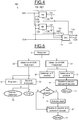
- FIG. 5 shows a flow diagram of the method in accordance with an embodiment of the invention.
- the step 1 comprises the reception of the modulated signal SIG by the antenna coil tag, which is modulated according to one protocol among the three protocols A, B and F.
- step 21 two steps are performed in parallel, step 21 and step 22.
- step 21 the modulated signal SIG is sent to the first demodulator DEM1 to detect if there is an ASK modulation.
- step 22 the modulated signal SIG is sent to the second demodulator DEM2 to detect if there is an OOK modulation.
- the first signal SIG1 is sent to the first block RB to detect, in step 31, if the modulated signal is modulated according to the type B protocol.
- the first signal SIG1 will be memorized in a flip-flop or a latch and will be sent to the second block RF to detect, in step 32, if the modulated signal is modulated according to the type F protocol.
- step 41 decoder DB is activated and the decoder DA is disabled in case protocol B has been detected.
- the decoder decodes said data stream in step 71.
- control means MC verify if the clock signal CLK is stopped in step 5. If that is the case, said control means disable, in step 6, the stopping module ST to let the clock signal CLK run again.
- the decoder DF is then activated in step 42 and the decoder DA disabled. Thus, the decoder will decode said data stream in step 72.
- the decoder DF is activated in step 42 to decode in step 72 said data stream.
- said second signal SIG2 is sent to the decoder DA in step 33 to decode said second signal which is memorized by said memory means MMA which can be a flip-flop or a latch.
- said blocking module ST stops the clock signal in step 34 until the reception of a non-modulated signal.
- the blocking module ST doesn't stop the clock signal and the memorized second signal SIG2 will be decoded.
- step 73 the decoder cannot decode said data stream, this means that the modulated signal SIG has been modulated according to type F protocol.
- the system will wait in step 73 for the detection of type F protocol by the second block RF in step 32 and then if type F protocol has been successfully detected, the clock signal is no longer stopped during said modulated pulses, as explained in step 6.
Landscapes
- Engineering & Computer Science (AREA)
- Computer Networks & Wireless Communication (AREA)
- Signal Processing (AREA)
- Physics & Mathematics (AREA)
- Theoretical Computer Science (AREA)
- Health & Medical Sciences (AREA)
- General Physics & Mathematics (AREA)
- Toxicology (AREA)
- General Engineering & Computer Science (AREA)
- Computer Security & Cryptography (AREA)
- Electromagnetism (AREA)
- General Health & Medical Sciences (AREA)
- Artificial Intelligence (AREA)
- Computer Vision & Pattern Recognition (AREA)
- Digital Transmission Methods That Use Modulated Carrier Waves (AREA)
- Power Engineering (AREA)
- Communication Control (AREA)
Priority Applications (6)
| Application Number | Priority Date | Filing Date | Title |
|---|---|---|---|
| EP18178584.1A EP3584948A1 (de) | 2018-06-19 | 2018-06-19 | Protokolldetektion und -decodierung in einem multiprotokoll-etikett und entsprechende integrierte schaltung |
| US16/443,227 US10853593B2 (en) | 2018-06-19 | 2019-06-17 | Integrated circuits and methods for protocol detection and decoding in near field communications |
| CN202310104205.3A CN116112326B (zh) | 2018-06-19 | 2019-06-17 | 用于近场通信中的协议检测和解码的集成电路和方法 |
| CN201910521822.7A CN110620743B (zh) | 2018-06-19 | 2019-06-17 | 用于近场通信中的协议检测和解码的集成电路和方法 |
| CN201920906803.1U CN209994396U (zh) | 2018-06-19 | 2019-06-17 | 用于解码由调制信号承载的数据流的集成电路 |
| US17/102,917 US11423239B2 (en) | 2018-06-19 | 2020-11-24 | Integrated circuits and methods for protocol detection and decoding in near field communications |
Applications Claiming Priority (1)
| Application Number | Priority Date | Filing Date | Title |
|---|---|---|---|
| EP18178584.1A EP3584948A1 (de) | 2018-06-19 | 2018-06-19 | Protokolldetektion und -decodierung in einem multiprotokoll-etikett und entsprechende integrierte schaltung |
Publications (1)
| Publication Number | Publication Date |
|---|---|
| EP3584948A1 true EP3584948A1 (de) | 2019-12-25 |
Family
ID=62712893
Family Applications (1)
| Application Number | Title | Priority Date | Filing Date |
|---|---|---|---|
| EP18178584.1A Pending EP3584948A1 (de) | 2018-06-19 | 2018-06-19 | Protokolldetektion und -decodierung in einem multiprotokoll-etikett und entsprechende integrierte schaltung |
Country Status (3)
| Country | Link |
|---|---|
| US (2) | US10853593B2 (de) |
| EP (1) | EP3584948A1 (de) |
| CN (2) | CN110620743B (de) |
Cited By (1)
| Publication number | Priority date | Publication date | Assignee | Title |
|---|---|---|---|---|
| WO2023091867A1 (en) * | 2021-11-17 | 2023-05-25 | Battelle Energy Alliance, Llc | Observing signals in a network and/or identifying signaling protocols and related devices, systems, and methods |
Families Citing this family (7)
| Publication number | Priority date | Publication date | Assignee | Title |
|---|---|---|---|---|
| EP3584948A1 (de) | 2018-06-19 | 2019-12-25 | STMicroelectronics razvoj polprevodnikov d.o.o. | Protokolldetektion und -decodierung in einem multiprotokoll-etikett und entsprechende integrierte schaltung |
| US11720159B2 (en) * | 2019-07-01 | 2023-08-08 | Texas Instruments Incorporated | Unified bus architecture for a voltage regulator |
| US10720966B1 (en) * | 2019-07-22 | 2020-07-21 | Alibaba Group Holding Limited | Near field communication device and information processing method |
| US10789391B1 (en) * | 2019-07-22 | 2020-09-29 | Alibaba Group Holding Limited | RFID information processing |
| US20210350092A1 (en) * | 2020-05-09 | 2021-11-11 | Neology, Inc. | Control protocol for multi-protocol transponder |
| CN111800170A (zh) * | 2020-06-24 | 2020-10-20 | 易兆微电子(杭州)股份有限公司 | 一种用于负载调制的峰值检测方法 |
| CN117014845B (zh) * | 2023-09-22 | 2024-02-20 | 北京紫光青藤微系统有限公司 | 用于确定通信开始位置的方法、装置和近场通信设备 |
Citations (3)
| Publication number | Priority date | Publication date | Assignee | Title |
|---|---|---|---|---|
| US20160182263A1 (en) * | 2014-12-23 | 2016-06-23 | Qualcomm Incorporated | Systems and methods for switching quality factors during inductively coupled communications |
| EP3107208A1 (de) * | 2015-06-15 | 2016-12-21 | ams International AG | Demodulatorschaltung und verfahren zur demodulation |
| US20170053141A1 (en) * | 2010-06-22 | 2017-02-23 | Stmicroelectronics (Rousset) Sas | Method for managing communication between an electronic device, for example a contactless chip card, and a communication apparatus, for example a reader, and corresponding electronic device |
Family Cites Families (18)
| Publication number | Priority date | Publication date | Assignee | Title |
|---|---|---|---|---|
| US6249212B1 (en) * | 1994-10-05 | 2001-06-19 | Avid Marketing, Inc. | Universal electronic identification tag |
| CA2307361C (en) * | 2000-05-01 | 2008-04-08 | Mark Iv Industries Limited | Multiple protocol transponder |
| FR2831305B1 (fr) * | 2001-10-23 | 2004-01-30 | Inside Technologies | Circuit integre sans contact comprenant des moyens d'identification automatique de trame |
| KR100560770B1 (ko) * | 2003-09-15 | 2006-03-13 | 삼성전자주식회사 | 실시간 프로토콜 전환 기능을 갖는 비접촉 집적회로 카드및 그것을 포함한 카드 시스템 |
| US7583179B2 (en) * | 2005-02-22 | 2009-09-01 | Broadcom Corporation | Multi-protocol radio frequency identification transceiver |
| JP4313795B2 (ja) * | 2005-09-30 | 2009-08-12 | 富士通マイクロエレクトロニクス株式会社 | 非接触タグ、非接触タグの制御方法 |
| JP5295657B2 (ja) * | 2008-06-27 | 2013-09-18 | ルネサスエレクトロニクス株式会社 | 半導体集積回路、半導体集積回路を実装したicカードおよびその動作方法 |
| JP5225816B2 (ja) * | 2008-11-20 | 2013-07-03 | ルネサスエレクトロニクス株式会社 | 半導体装置 |
| KR101610916B1 (ko) * | 2010-02-23 | 2016-04-11 | 삼성전자주식회사 | 근거리 통신을 위한 수신 장치와 그에 따른 통신 모드 검출방법 |
| US8342415B2 (en) * | 2010-03-17 | 2013-01-01 | Inside Secure | Method of conducting a transaction using an NFC device |
| CN103457656A (zh) * | 2012-06-05 | 2013-12-18 | 武汉盛华微系统技术股份有限公司 | 适用于无线光纤覆盖系统的网管通道实现系统 |
| US9106268B2 (en) * | 2012-09-12 | 2015-08-11 | Qualcomm Incorporated | Methods and apparatus for improving acquisition for NFC load modulation |
| SI24283A (sl) * | 2013-01-15 | 2014-07-31 | Ams R&D Analogni Polprevodniki, D.O.O. | Postopek in vezje aktivne pametne nalepke za komuniciranje z izpraševalnikom |
| WO2015037187A1 (ja) * | 2013-09-11 | 2015-03-19 | パナソニックIpマネジメント株式会社 | 通信デバイス及び通信システム |
| CN104639482B (zh) * | 2013-11-12 | 2018-04-27 | 上海华虹集成电路有限责任公司 | 解码type b卡片发送的bpsk调制信号的解码器 |
| US20160057255A1 (en) * | 2014-08-22 | 2016-02-25 | Mediatek Inc. | Unified communications receiver and associated method |
| EP3528175B1 (de) * | 2018-02-15 | 2021-06-09 | Nxp B.V. | Taktstoppfrequenzeinstellung für einen transponder |
| EP3584948A1 (de) | 2018-06-19 | 2019-12-25 | STMicroelectronics razvoj polprevodnikov d.o.o. | Protokolldetektion und -decodierung in einem multiprotokoll-etikett und entsprechende integrierte schaltung |
-
2018
- 2018-06-19 EP EP18178584.1A patent/EP3584948A1/de active Pending
-
2019
- 2019-06-17 CN CN201910521822.7A patent/CN110620743B/zh active Active
- 2019-06-17 US US16/443,227 patent/US10853593B2/en active Active
- 2019-06-17 CN CN201920906803.1U patent/CN209994396U/zh active Active
-
2020
- 2020-11-24 US US17/102,917 patent/US11423239B2/en active Active
Patent Citations (3)
| Publication number | Priority date | Publication date | Assignee | Title |
|---|---|---|---|---|
| US20170053141A1 (en) * | 2010-06-22 | 2017-02-23 | Stmicroelectronics (Rousset) Sas | Method for managing communication between an electronic device, for example a contactless chip card, and a communication apparatus, for example a reader, and corresponding electronic device |
| US20160182263A1 (en) * | 2014-12-23 | 2016-06-23 | Qualcomm Incorporated | Systems and methods for switching quality factors during inductively coupled communications |
| EP3107208A1 (de) * | 2015-06-15 | 2016-12-21 | ams International AG | Demodulatorschaltung und verfahren zur demodulation |
Cited By (1)
| Publication number | Priority date | Publication date | Assignee | Title |
|---|---|---|---|---|
| WO2023091867A1 (en) * | 2021-11-17 | 2023-05-25 | Battelle Energy Alliance, Llc | Observing signals in a network and/or identifying signaling protocols and related devices, systems, and methods |
Also Published As
| Publication number | Publication date |
|---|---|
| CN116112326A (zh) | 2023-05-12 |
| US20190384951A1 (en) | 2019-12-19 |
| US20210081622A1 (en) | 2021-03-18 |
| US11423239B2 (en) | 2022-08-23 |
| US10853593B2 (en) | 2020-12-01 |
| CN209994396U (zh) | 2020-01-24 |
| CN110620743A (zh) | 2019-12-27 |
| CN110620743B (zh) | 2023-03-24 |
Similar Documents
| Publication | Publication Date | Title |
|---|---|---|
| US11423239B2 (en) | Integrated circuits and methods for protocol detection and decoding in near field communications | |
| US8325786B2 (en) | Semiconductor device and communication device | |
| US20070026825A1 (en) | NFC device and apparatus | |
| US10049237B2 (en) | Radio-frequency identification transponder and method for sending a radio-frequency identification message | |
| US8250451B2 (en) | IC card, information processing device, communication type identification method, and program | |
| CN101826898B (zh) | 通信设备和通信方法 | |
| US7252241B2 (en) | Data communication system, data communication device, contactless communication medium, and communication device control program | |
| EP0967562B1 (de) | Übertragungsverfahren | |
| US20150180546A1 (en) | Detection of Load-Modulated Signals in NFC | |
| US20160117535A1 (en) | Non-contact communication method determination circuit, non-contact communication circuit, and ic card | |
| US11416692B2 (en) | Method for distinguishing between active and passive contactless devices, and corresponding reader | |
| JP5428364B2 (ja) | 非接触型通信装置、その復号部 | |
| US20130083787A1 (en) | Configuration of a near-field communication router according to the modulation type | |
| CN116112326B (zh) | 用于近场通信中的协议检测和解码的集成电路和方法 | |
| US8310345B2 (en) | Receiving apparatus | |
| US20060158243A1 (en) | Amplitude demodulator for an electromagnetic transponder | |
| EP3809329B1 (de) | Taktwiederherstellung in einem rfid-transponder | |
| EP3584949A1 (de) | Verfahren zur begrenzung des pegels eines modulierten signals, das durch ein etikett empfangen wird, und zugehöriger begrenzer | |
| WO2008140156A1 (en) | Rf reader capable of detecting rf signal and existence of rf card and the method thereof | |
| US11855713B2 (en) | Method for implementing an NFC transaction | |
| JP2005151075A (ja) | Rfid通信におけるパルスギャップ信号による非同期通信方式 | |
| JP2012068932A (ja) | 非接触型icカード | |
| KR100827283B1 (ko) | 복합 rfid 리더 및 그의 동작 방법 | |
| CN115765801A (zh) | 用于数字调制信号的具有干扰滤波器的rfid ic | |
| US20050219038A1 (en) | Method and system for contactless data transmission |
Legal Events
| Date | Code | Title | Description |
|---|---|---|---|
| PUAI | Public reference made under article 153(3) epc to a published international application that has entered the european phase |
Free format text: ORIGINAL CODE: 0009012 |
|
| STAA | Information on the status of an ep patent application or granted ep patent |
Free format text: STATUS: THE APPLICATION HAS BEEN PUBLISHED |
|
| AK | Designated contracting states |
Kind code of ref document: A1 Designated state(s): AL AT BE BG CH CY CZ DE DK EE ES FI FR GB GR HR HU IE IS IT LI LT LU LV MC MK MT NL NO PL PT RO RS SE SI SK SM TR |
|
| AX | Request for extension of the european patent |
Extension state: BA ME |
|
| STAA | Information on the status of an ep patent application or granted ep patent |
Free format text: STATUS: REQUEST FOR EXAMINATION WAS MADE |
|
| 17P | Request for examination filed |
Effective date: 20200319 |
|
| RBV | Designated contracting states (corrected) |
Designated state(s): AL AT BE BG CH CY CZ DE DK EE ES FI FR GB GR HR HU IE IS IT LI LT LU LV MC MK MT NL NO PL PT RO RS SE SI SK SM TR |
|
| STAA | Information on the status of an ep patent application or granted ep patent |
Free format text: STATUS: EXAMINATION IS IN PROGRESS |
|
| 17Q | First examination report despatched |
Effective date: 20210504 |
|
| STAA | Information on the status of an ep patent application or granted ep patent |
Free format text: STATUS: EXAMINATION IS IN PROGRESS |