EP3582396A1 - Configurable integrated desaturation filter - Google Patents
Configurable integrated desaturation filter Download PDFInfo
- Publication number
- EP3582396A1 EP3582396A1 EP19020380.2A EP19020380A EP3582396A1 EP 3582396 A1 EP3582396 A1 EP 3582396A1 EP 19020380 A EP19020380 A EP 19020380A EP 3582396 A1 EP3582396 A1 EP 3582396A1
- Authority
- EP
- European Patent Office
- Prior art keywords
- signal
- filter
- coupled
- time constant
- detector
- Prior art date
- Legal status (The legal status is an assumption and is not a legal conclusion. Google has not performed a legal analysis and makes no representation as to the accuracy of the status listed.)
- Granted
Links
Images




Classifications
-
- H—ELECTRICITY
- H03—ELECTRONIC CIRCUITRY
- H03K—PULSE TECHNIQUE
- H03K17/00—Electronic switching or gating, i.e. not by contact-making and –breaking
- H03K17/08—Modifications for protecting switching circuit against overcurrent or overvoltage
- H03K17/082—Modifications for protecting switching circuit against overcurrent or overvoltage by feedback from the output to the control circuit
- H03K17/0826—Modifications for protecting switching circuit against overcurrent or overvoltage by feedback from the output to the control circuit in bipolar transistor switches
-
- H—ELECTRICITY
- H03—ELECTRONIC CIRCUITRY
- H03K—PULSE TECHNIQUE
- H03K17/00—Electronic switching or gating, i.e. not by contact-making and –breaking
- H03K17/16—Modifications for eliminating interference voltages or currents
- H03K17/168—Modifications for eliminating interference voltages or currents in composite switches
-
- H—ELECTRICITY
- H03—ELECTRONIC CIRCUITRY
- H03K—PULSE TECHNIQUE
- H03K17/00—Electronic switching or gating, i.e. not by contact-making and –breaking
- H03K17/04—Modifications for accelerating switching
- H03K17/0406—Modifications for accelerating switching in composite switches
-
- H—ELECTRICITY
- H03—ELECTRONIC CIRCUITRY
- H03K—PULSE TECHNIQUE
- H03K17/00—Electronic switching or gating, i.e. not by contact-making and –breaking
- H03K17/08—Modifications for protecting switching circuit against overcurrent or overvoltage
- H03K17/081—Modifications for protecting switching circuit against overcurrent or overvoltage without feedback from the output circuit to the control circuit
- H03K17/0812—Modifications for protecting switching circuit against overcurrent or overvoltage without feedback from the output circuit to the control circuit by measures taken in the control circuit
- H03K17/08122—Modifications for protecting switching circuit against overcurrent or overvoltage without feedback from the output circuit to the control circuit by measures taken in the control circuit in field-effect transistor switches
-
- H—ELECTRICITY
- H03—ELECTRONIC CIRCUITRY
- H03K—PULSE TECHNIQUE
- H03K17/00—Electronic switching or gating, i.e. not by contact-making and –breaking
- H03K17/08—Modifications for protecting switching circuit against overcurrent or overvoltage
- H03K17/081—Modifications for protecting switching circuit against overcurrent or overvoltage without feedback from the output circuit to the control circuit
- H03K17/0812—Modifications for protecting switching circuit against overcurrent or overvoltage without feedback from the output circuit to the control circuit by measures taken in the control circuit
- H03K17/08128—Modifications for protecting switching circuit against overcurrent or overvoltage without feedback from the output circuit to the control circuit by measures taken in the control circuit in composite switches
-
- H—ELECTRICITY
- H03—ELECTRONIC CIRCUITRY
- H03K—PULSE TECHNIQUE
- H03K17/00—Electronic switching or gating, i.e. not by contact-making and –breaking
- H03K17/16—Modifications for eliminating interference voltages or currents
- H03K17/161—Modifications for eliminating interference voltages or currents in field-effect transistor switches
- H03K17/162—Modifications for eliminating interference voltages or currents in field-effect transistor switches without feedback from the output circuit to the control circuit
-
- H—ELECTRICITY
- H03—ELECTRONIC CIRCUITRY
- H03K—PULSE TECHNIQUE
- H03K17/00—Electronic switching or gating, i.e. not by contact-making and –breaking
- H03K17/18—Modifications for indicating state of switch
-
- H—ELECTRICITY
- H03—ELECTRONIC CIRCUITRY
- H03K—PULSE TECHNIQUE
- H03K17/00—Electronic switching or gating, i.e. not by contact-making and –breaking
- H03K17/51—Electronic switching or gating, i.e. not by contact-making and –breaking characterised by the components used
- H03K17/56—Electronic switching or gating, i.e. not by contact-making and –breaking characterised by the components used by the use, as active elements, of semiconductor devices
- H03K17/567—Circuits characterised by the use of more than one type of semiconductor device, e.g. BIMOS, composite devices such as IGBT
-
- H—ELECTRICITY
- H03—ELECTRONIC CIRCUITRY
- H03K—PULSE TECHNIQUE
- H03K2217/00—Indexing scheme related to electronic switching or gating, i.e. not by contact-making or -breaking covered by H03K17/00
- H03K2217/0027—Measuring means of, e.g. currents through or voltages across the switch
Definitions
- the present invention relates generally to a system and method for providing a configurable integrated DESAT (desaturation region) filter for an IGBT or MOSFET.
- DESAT deaturation region
- Switches such as IGBTs or MOSFETs must be protected against overload conditions due to, for example, an overcurrent condition, otherwise excessive heating and subsequent damage to the switches can occur.
- Figure 1A is a plot of the typical output characteristics of an IGBT at 25 °C, wherein the collector current (I C ) is plotted against the collector-emitter-voltage (V CE ).
- Curve 102A demarcates a first operating region 106 wherein the switch exhibits a bulk resistor voltage drop, and a second operating region 108 designated the desaturation region.
- Figure 1B is a plot of the typical output characteristics of an IGBT at 175 °C, wherein the collector current (I C ) is plotted against the collector-emitter-voltage (V CE ).
- Curve 102B demarcates the first operating region 106 wherein the switch exhibits a bulk resistor voltage drop, and the second operating region 108 designated the desaturation region.
- V CE collector-emitter-voltage
- MOSFETs react to an overcurrent event with an increase of the drain-source-voltage V DS according to the resistive voltage drop across the ON-resistance. With increased current the MOSFET saturates until the current is limited or until V DS reaches the supply voltage (DC-link voltage).
- V CE voltage is measured in the IGBT conduction state via a high voltage blocking element. In the IGBT blocking state the high voltage blocking element decouples the sensing input from the high IGBT blocking voltage. Therefore the voltage VCE is measured in a voltage range up to approximately six to nine volts directly.
- a DESAT event is a major failure for an application, which typically requires a time consuming restart. Therefore false detection should be prevented as well as a false "no detection" of a DESAT event, which may lead to a destruction of the switch.
- the driver is frequently placed in a noisy environment. This leads to the need to filter the DESAT input against noise, spikes and other disturbances. This, in turn, leads to limitations on how fast the DESAT detection can occur. Due to this limitation in speed, recurring shorts for shorter duration ON pulses cannot be detected. If this condition continues for many consecutive pulses it might lead to a successive rise in temperature of the switch and eventual damage.
- a system comprises a control circuit having a plurality of detectors coupled to a first node of the control circuit, a plurality of filters coupled to the plurality of detectors, and a logic circuit coupled to the first and second filters, a diode circuit having a first node coupled to the first node of the control circuit, and a switch having a first current node coupled to a second node of the diode circuit, a gate coupled to a second node of the control circuit, and a second current node coupled to a third node of the control circuit wherein a first detector of the plurality of detectors is configured to provide a first event overcurrent signal and at least a second detector of the plurality of detectors is configured to provide a multiple event overcurrent signal or a warning signal.
- the first detector has a first detection threshold, and the second detector has a second detection threshold equal to or different from the first detection threshold.
- the first filter has a first time constant, and the second filter has a second time constant equal to or different from the first time constant.
- a clamping transistor is coupled between the first and third nodes of the control circuit.
- the diode circuit comprises a resistor and diode coupled in series.
- the second detector can be configured to provide margin testing of a performance criterion of the first detector.
- the first and second detectors can be configured to provide an overcurrent signal or a warning signal during a two-level turnoff plateau operating mode of the system.
- a circuit comprises a plurality of detectors coupled to a first node, wherein a first detector of the plurality of detectors has a first programmable detection threshold, and a second detector of the plurality of detectors has a second programmable detection threshold equal to or different from the first detection threshold, a plurality of filters coupled to the plurality of detectors, wherein a first filter of the plurality of filters has a first programmable time constant, and a second filter of the plurality of filters has a second programmable time constant equal to or different from the first time constant, and a logic circuit having an input coupled to the plurality of filters and an output coupled to a second node coupled to a switch, wherein the first detector of the plurality of detectors is configured to provide a first event overcurrent signal and at least the second detector of the plurality of detectors is configured to provide a multiple event overcurrent signal or a warning signal. At least one of the first and second detectors comprise a comparator coupled to a first programmable detection threshold, and a second
- a method comprises detecting an input signal using a first threshold to generate a first detected signal, detecting the input signal using a second threshold to generate a second detected signal, filtering the first detected signal using a first time constant to generate a first filtered signal, filtering the second detected signal using a second time constant to generate a second filtered signal, using the first filtered signal to generate a first event overcurrent signal, and using at least the second filtered signal to generate either a multiple event overcurrent signal or a warning signal.
- the method further comprises controlling an operating mode of a switch using the overcurrent signal.
- the method further comprises counting a plurality of overcurrent events associated with the input signal before generating the multiple event overcurrent signal or the warning signal.
- Filtering the first detected signal comprises filtering the first detected signal with a first filtering method
- filtering the second detected signal comprises filtering the second detected signal with a second filtering method.
- the method is performed in a switching system, and includes counting a plurality of overcurrent events associated with the input signal to enable margin testing of at least one performance criterion of the switching system.
- the multiple event overcurrent signal or warning signal can be generated during a two-level turn-off plateau operating mode of the switching system.
- the method can further include detecting the input signal using a plurality of thresholds to generate a plurality of detected signals, and filtering the plurality of detected signals using a plurality of time constants to generate a plurality of filtered signals. At least one of the first threshold, second threshold, first time constant, and second time constant are programmable.
- At least one additional DESAT detector allows for additional modes of operation for controlling a switch during one or more overcurrent events.
- An additional DESAT detector with a lower detection threshold and filter time as other parallel DESAT detectors can be used as a margin indicator for assessing system performance rather than a protection element.
- the use of an additional DESAT detector can also be used to detect shorter short-circuit events and where the number of detected shorter short-circuit events over several PWM cycles can be counted to determine if the turn-on operation of the driven switch should be prevented.
- the use of an additional DESAT detector can be used during a two-level turn-off plateau to generate an overcurrent signal or warning signal.
- DESAT detection and filtering circuits and implementations are described below that are suitable for use with an embodiment of the configurable integrated desaturation filter of the invention.
- the circuits of Figures 2 and 3 use a high voltage diode as blocking element.
- the VCE voltage is measured in the IGBT conduction state (ON state) via a high voltage blocking diode biased by a current. Therefore the voltage VCE plus the forward voltage of the diode is measured in a voltage range.
- the threshold voltage for detection is approximately six to nine volts for an IGBT switch and approximately two volts to nine volts for a MOSFET switch. Higher voltages are an indication of a desaturation event. A comparator detects this and reports the event. In the OFF state the high voltage blocking diode decouples the sensing input from the high IGBT blocking voltage at the collector.
- the filtering of the DESAT input can be realized with a small capacitor.
- the time constant of the filter determines the time it takes to charge the capacitance at the DESAT pin to a comparator voltage trigger level (defined herein as "filter time”). Due to this, the filter time is impacted by the variation of the current that charge the capacitance, the variation of the value of the capacitance, the variation of the comparator trip level and the pre-charged voltage level the capacitance has at the point in time when the short circuit of the switch happens.
- the pre-charged voltage level depends on the loading of the switch and if the current is positive or negative through the switch (or diode for the IGBT).
- the charging current can be implemented as a simple pull up resistor (see Figure 2 ), which results in a flat charging curve at the detection threshold due to the RC filtering nature. Therefore this solution has a high sensitivity to noise around the trip point and high sensitivity for the filter time variation due to comparator detection level variations. Low spread resistances are inexpensive, but the charging current and the filter time are sensitive to supply voltage variation. However, the charging current dependent losses are dissipated in the resistor.
- FIG. 2 shows a control circuit 202 including V CC2 , DESAT, OUT, and GND2 pins.
- Control circuit also includes a comparator 204 for monitoring the voltage on the DESAT pin, and a clamping transistor 206 coupled between the DESAT and GND2 pins for clamping the DESAT pin to the GND2 pin voltage.
- the clamp transistor 206 may be released at the same time or be released at a determined time after the turn on of switch 208.
- the clamp transistor 206 is activated at the same time as the turn off command.
- the command signals for a turn off of switch 208 come at the same time as the activation command for clamp 206. In some embodiments, the turn off of switch 208 is artificially delayed.
- Figure 2 also includes a filter capacitor CV CC2 coupled between the V CC2 pin and the GND2 pin, a gate resistor RG coupled between the OUT pin and the gate 214 of IGBT 208.
- IGBT 208 is also coupled to a recirculation diode 210 at collector node 212 and emitter node 216.
- the pullup resistor R PULLUP is coupled between the V CC2 pin and the DESAT pin.
- a DESAT resistor R DESAT and a DESAT diode D DESAT are coupled between the DESAT pin and the collector 212 of IGBT 208.
- the charging current can also be implemented as an integrated current source (see Figure 3 ).
- the filter time constant depends on the accuracy of the current source.
- a constant voltage ramp makes the dv/dt of the voltage ramp steeper around the comparator trip point compared to the exponential charging in the resistor case described above.
- Ramp-up and settling time of the current source introduces a potential error to the filter time if it needs to be used directly after the activation of the power switch. Robustness of the current source against voltages at the DESAT pin above driver supply and below emitter potentials is required, which can cause latch up or other disturbances of the operation of the circuit.
- Figure 3 includes substantially the same components as those described above with respect to the circuit of Figure 2 , except for the addition of the integrated current source 232 coupled between the VCC2 and DESAT pins.
- the capacitance at the DESAT pin includes the discrete capacitor CDESAT and the charge on the high voltage diode DDESAT. Due to the limited charging current in the current source circuit of Figure 3 (up to few hundred ⁇ A) and the small filter time (up to a few ⁇ s) the DESAT filter capacitor CDESAT has to be small, typically in the range of 50 pF to 250 pF.
- the accuracy of the capacitance (and the filter) is influenced by layout capacitance, environmental effects like bedewing, charge variation of the high voltage diode charge of possibly used protection diodes, and leakage currents of possibly used protection diodes.
- FIG. 4 An alternative detection and filtering method uses a voltage divider and clamping diode in order not to use a high voltage diode, as can be seen in the schematic of Figure 4.
- Figure 4 includes substantially the same components as those described above with reference to the circuits of Figures 2 and 3 , except for the use a clamping diode DCLAMP, and two separate DESAT resistors RDESAT1 and RDESAT2. Resistors RDESAT1 and RDESAT2 are coupled between the DESAT pin and the collector 212 of IGBT 208. Diode DCLAMP is coupled between the VCC2 pin and the intermediate node 234.
- the clamp transistor 206 When IGBT 208 is in the off state the clamp transistor 206 is activated to clamp the input of the comparator 204 to oV.
- the VCE voltage of the IGBT 208 can either be a few volts negative or at a high voltage potential, for example 800V, depending on the load current direction.
- the diode DCLAMP will be forward biased or reverse biased. The resistance needs to be high in order not to consume too much power in the resistors in the off state.
- the IGBT 208 When the IGBT 208 is turned on the VCE voltage goes down to a VCE,SAT voltage. At the same time or shortly thereafter the clamp transistor releases the clamping of the comparator input (DESAT pin).
- the filter time is defined by the series resistance of RDESAT1 and RDESAT2, the capacitance at the DESAT pin including any deliberately placed capacitance CDESAT and any additional parasitic capacitance (from the comparator input, the printed circuit board, etc.), the comparator trip level, and the pre-charged voltage level depending on the loading of the switch. Due to the high resistance in series from the collector to the comparator input, the total capacitance at the DESAT pin has to be very low and therefore any variations of the parasitic capacitances will have a high impact on the total capacitance.
- VCE voltage will increase to a level higher than the threshold of the comparator 204 and the comparator will trigger and turn off the IGBT 208.
- VCE voltage can also become so high during the desaturation event that the voltage becomes higher than the power supply of the gate driver (VCC2).
- the diode DCLAMP and resistor RDESAT1 will protect the driver form the potentially destructive voltage level at the collector 212 of IGBT 208.
- the diode DCLAMP clamps node 234 between resistor RDESAT2 and RDESAT1 to a voltage of VCC2 + Vth of the diode, and a current will flow from the collector 212 through resistor RDESAT1 and through the diode DCLAMP to the power supply VCC2.
- a resistance can be placed in parallel to capacitor CDESAT in order to create a resistor divider together with the RDESAT1 and RDESAT2. In this manner VCE DESAT levels placed higher than the VCC2 level can be used. This can be of importance if the DESAT detection is to be used for switches able to block voltages higher than, for example, 1700 V.
- the absolute size of the DESAT capacitance limits the performance of filtering against spikes or coupling from a noisy environment. Additionally filtering at one input with one capacitor gives exactly one time constant. Higher level filtering or parallel detection of a different threshold or filter time combination with one blocking structure (high voltage blocking diode or resistive) is not possible. Additionally the number of different components and configurations that impact the actual filter time results in a great deal of variation in the filter time.
- two or more independent DESAT levels and filter values are used at the same time sharing the same blocking structure.
- the filters can be coupled to the comparator outputs, which are in turn coupled to a logic circuit.
- a DESAT detection structure or circuit with one or more independently configurable voltage threshold levels and filter times is used to detect various short circuit and overcurrent events and to provide various signals in response as described herein using only one pin, one resistor and one diode to decouple a DESAT pin from the collector or drain potential of the driven switch in the off state.
- a desaturation detection can be done without the use of a diode.
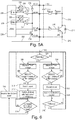
- Figure 5A a circuit according to an embodiment of the invention is shown where the filter is located after the comparator and the reference for (in this case two) comparators is set by a DAC.
- Figure 5A thus shows a controller circuit 202 including the VCC2, DESAT, OFF and GND2 pins, filter capacitor CVCC2, gate resistor RG, DESAT resistor RDESAT, DESAT diode DDESAT, clamping transistor 206, integrated current source 232, and IGBT 208/recirculation diode 210 as previously shown with respect to the circuits shown in Figures 2-4 .
- the circuit of Figure 5A includes a logic circuit 226 including first and second filters 228 and 230, first and second comparators 220 and 224, and first and second DACs 218 and 222. Note that an input of both comparators 220 and 224 are coupled to the DESAT pin.
- DAC 218 provides the threshold voltage for comparator 220, and DAC 222 provides the threshold voltage for comparator 224.
- the output of comparator 220 is coupled to the first filter 228, and the output of comparator 224 is coupled to the second filter 230.
- the driver can be set up to cover a wider range of DESAT detection cases and increase the detection range from only short circuit protection to overcurrent detection (even for bipolar devices, or IGBTs).
- Hard-short circuitry with a steep current slope is handled from one DESAT filter time/voltage threshold setting.
- fast desaturation and high overload DC-Link voltage multiplied by the short circuit current
- a soft overload (overcurrent) with a slow current rise is handled from the other DESAT filter time/voltage threshold setting.
- a slow current rise a slowly increasing overload (slightly increasing saturation voltage times up to a short circuit current) allows for a longer filter time and a lower detection voltage.
- Having an internal filter also enables an implementation that has an adjustable DESAT detector (software adjustable) for which parameters (detection voltage and filter time) can be changed without changing the external circuitry. This feature enables late design changes without a corresponding hardware population change.
- the adjustable filter may be of an analog or digital solution. Adjustability is not specifically required, and fixed values can be used as well.
- An internal filter also enables the possibility of using different filter algorithms or filter orders optimized for each detection case, e.g. for equal distributed noise floor an up/down counter can be used, and for fastest reaction an up/reset counter can be used. Other algorithms can also be used to provide other features and functions.
- Different filter types that can be used according to embodiments can include, but are not limited to passive or active; analog or digital; high-pass, low-pass, band-pass, band-stop, or all-pass; discrete-time or continuous-time; linear or non-linear; or infinite impulse response or finite impulse response. Filter types can be classified in numerous other ways by those skilled in the art including by transfer function, filter topology, hardware filter technology, and in many other ways.
- adjustable comparator a voltage measured at the DESAT pin is measured with a fast analog-to-digital converter ("ADC") and a digital filter is applied afterwards.
- ADC analog-to-digital converter
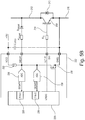
- Figure 5B thus shows an implementation using two ADCs 236 and 238 having an analog input coupled to the DESAT pin.
- the digital output of ADC 236 designated DESAT1 is coupled to the input of the first filter 228.
- the digital output of ADC 238 designated DESAT2 is coupled to the input of the second filter 230.
- the threshold can be a digital numerical comparison of the ADC word or the word after a filter.
- the filter can be placed after the ADC before a numerical comparison or after the numerical comparison.
- the comparison level is programmable by changing the word that the ADC or filter word should be compared to. If the comparison is done before the filter, the filter is done on a one bit data stream. If the filter is done before the comparison the filter is a numerical filter such as a classical low pass filter.
- Configuring the threshold by the customer is only one option. It is as well possible to preconfigure a driver to the most relevant used cases and sell as one completely integrated part which reacts on different failure cases.
- DESAT2 additional DESAT detector results
- DESAT1 traditional DESAT detection that turns off the driven switch when a desaturation is detected
- DESAT1 More than one DESAT detector can be used for slow and fast short circuit detection, according to embodiments.
- any of the above described DESAT detection methods can be used, for example external filtering without sharing the blocking element or internal filtering where sharing of the blocking element can be used, high voltage diode blocking or voltage divider and clamping diode.
- DESAT1 DESAT1 9V threshold and 5 ⁇ s filter time
- DESAT2 7V threshold DESAT2 7V threshold and/or 3 ⁇ s filter time
- DESAT2 is configured in a way that a DESAT2 event's does not lead to a fault turn off.
- DESAT2 is configured to count DESAT2 events in a DESAT2 counter. The counter value can be monitored by the controller without stopping and endangering the system. The counter value together with the set margin of the thresholds gives an indication for system stability.
- the DESAT1 value is chosen to be, for example, 9 volts.
- the number of triggering DESAT2 events gives an indication of how close or far away the DESAT2 level is from the real margin value. If the margin is judged to be too high then the DESAT1 level can be potentially reduced. If the margin is judged to be too low then the DESAT1 level can be increased. Filter time can be tested and adjusted in a similar manner as described above.
- a flow diagram of a margin test method is shown in Figure 6 .
- the flow diagram for the margin test begins at 302.
- Step 304 interrogates whether or not the PWM signal used in the switch is high or not. If no, the method returns to 302. If yes, in the DESAT1 path described above, the V CE voltage is measured at 306.
- the method determines whether or not the DESAT1 voltage is great than the DESAT1 threshold, and whether or not a signal is present at the output of the first filter. If yes, than a DESAT1 event is determined to have happened at 310. If no, than the method returns to 302. If a DESAT1 event has happened, then the switch is turned off and the PWM signal is set low at 312.
- step 304 interrogates whether or not the PWM signal used in the switch is high or not. If yes, simultaneously in the DESAT2 path described above, the V CE voltage is measured at 318.
- the method determines whether or not the DESAT2 voltage is great than the DESAT2 threshold, and whether or not a signal is present at the output of the second filter. If yes, than a DESAT2 event is determined to have happened at 322. If no, than the method returns to 302. If a DESAT2 event has happened, then the DESAT2 counter is incremented at 324. At 326, the method waits for the PWM signal to be set low, and the method further continues back to 302 when the PWM signal is in fact set low.
- Another application of an embodiment of the invention is short circuit detection during repetitive short pulse operation (e.g. sinusoidal pulse width modulation).
- short PWM ON pulses with repetitive DESAT events e.g. sinusoidal pulse width modulation
- standard DESAT minimal filter time is limited due to noise in the system.
- PWM ON pulses shorter than minimal filter time cannot be detected, and otherwise false triggering of a DESAT event can happen.
- Short short-circuit events typically do not destroy the switch immediate by current destruction, but the switch is heated up during short circuit events. If a switch has a total short circuit rating of 10 ⁇ s, this means that the switch is destroyed after 10 ⁇ s with a nominal short circuit current.
- a short circuit event that is shorter than 10 ⁇ s heats up the switch, but does not destroy the switch.
- 10 ⁇ 1 ⁇ s short circuit events can have a similar thermal impact as one 10 ⁇ s short circuit event. If the driver detects ten consecutive short circuit events it can switch off the switch before destruction. This means not every detected DESAT event requires a driver switch off, but the driver can be made to count a certain number of short repetitive DESAT events until the switch reaches the maximum junction temperature. Counter overflow by noise is prevented by decrementing of the counter with N PWM pulses, according to an embodiment of the invention.
- Standard DESAT1 detection uses a certain known filter length. At one side the filter has to be as short as possible to protect for small pulses, at the other side it has to protect against false triggering. Every detected DESAT1 event leads to a fault turn off. Pulses shorter than minimal filter time cannot be detected (e.g. DESAT1 9V threshold and 5 ⁇ s filter time). For a second/additional DESAT set up (here called DESAT2) other rules can be applied. For example, not every detected DESAT2 event leads to a fault turn off. Shorter filter time than DESAT1 can be used (e.g. 9V threshold and 3 ⁇ s filter time). To prevent false triggering, a second higher level filtering is added.
- DESAT2 Counting of DESAT2 events and counter decrement after N-PWM pulses without DESAT events (e.g. 4, not effective in Figure 7 , no decrement due to max count of 2).
- the driver After a maximal number of DESAT2 events the driver will switch off with fault turn off (e.g. 2)
- DESAT2 can be configured as warning only, this means no fault off is initiated, the system controller can read out the warning bits regularly
- a minimum DESAT1 filter time 402 is shown determined by system noise. Non-detectable pulses occurring during time period 404 associated with the PWM waveform 406 are shown. Six such non-detectable pulses are shown during time period 404, since these pulses have a pulse width smaller than the DESAT1 filter time. Nonetheless, the operating temperature 408, TJ, of the switch is shown to be increasing during time period 404 after the point in time when the short circuit occurs.
- a minimum DESAT2 filter time 410 is shown that is smaller than the filter time 402 of the DESAT1 filter time.
- two DESAT2 short circuit events are determined, and are shown as counted DESAT2 events 414.
- time period 412 also associated with PWM waveform 406, two PWM counts 416 occur associated with non-detectable short circuit events (by either the DESAT1 or DESAT2 filter).
- the short circuit detection method is further explained with reference to the flow diagram of Figure 8 .
- the DESAT1 and DESAT2 paths are substantially the same as previously described with respect to the margin testing method described above with respect to Figure 6 .
- the DESAT2 path includes a further step 328 that interrogates whether or not the DESAT2 counter has reached a maximum number of DESAT2 events. If yes, then the method proceeds to 312 in the DESAT1 path as previously described. If no, then the method continues to 326 in the DESAT2 path as previously described.
- a parallel monitoring path is used to decrement the DESAT2 counter for sub-DESAT2 short circuit events.
- Step 330 is associated with a reset of the DESAT2 event.
- Step 346 checks to see that the PWM signal has been set low.
- Step 334 interrogates whether or not the PWM signal is low and whether or not there is a DESAT2 event.
- Step 342 increments a DESAT free counter.
- step 344 which interrogates whether or not the DESAT free counter has reached a predetermined limit or not. If no, the method returns to 332. If yes, the method continues to step 336. Step 336 interrogates whether or not the DESAT2 counter is greater than zero. If not, the method returns to 332. If yes, then the DESAT2 counter is decremented at 338, and the method returns to 332.
- a third application of an embodiment of the invention is detecting overcurrent events during a two-level turn-off phase.
- the gate voltage of the power switch is first reduced to a defined level (plateau) and the switch is turned off after a certain time (plateau time) has elapsed.
- This mechanism is called "two-level turn off (2LTO or TLTOff).
- two-level turn off methods may be applied to driving IGBT switches in order avoid latch-up of the switching transistor under high current conditions.
- Standard DESAT detection is inactive during two-level turn-off (TLTOff) due to several reasons.
- the normal DESAT filter time is in most cases longer than a TLTOff plateau time and therefore not able to detect a desaturation during that time, but it is also not desirable to turn off every time the IGBT goes in to desaturation during the TLTOff.
- either the input or output of the comparator is blocked during the TLTOff plateau time.
- Standard DESAT1 detection uses a certain filter length and voltage threshold. And at detection, a fault off is executed. During the TLTOff plateau the output of the DESAT1 comparator is blocked.
- the IGBT may go in to an overload condition leading to a desaturation due to the reduced gate voltage.
- DESAT events during TLTOff does not lead to an immediate destruction (compared to nominal short circuit the maximum collector current is much lower (e.g. 4x) and therefore the short circuit withstand time is enlarged (e.g. 4x)).
- a thermal destruction of the IGBT over several PWM cycles is the typical failure case. To protect the switch against this overload scenario, the same measures as explained above with reference to the repetitive short circuit condition can be taken.
- DESAT2 Not every detected DESAT2 event leads to a fault turn off.
- a shorter filter time than DESAT1 can be used (e.g. 9V threshold and 2 ⁇ s filter time).
- a second high level filtering added.
- Counting of DESAT2 events and a counter decrement after N-PWM pulses without DESAT events (e.g. 4) is used.
- the driver After a maximal number of DESAT2 events the driver will switch off with fault turn off (e.g. 2).
- DESAT2 can be configured as a warning only. This means no fault off is initiated, and the system controller can read out the warning bits regularly.
- the first event overcurrent signal is typically a single event signal due to a single pulse overcurrent condition, but the first event overcurrent signal could also include a response to a double or multiple pulse event, or any other overcurrent event, in an embodiment.
- the multiple event overcurrent signal may be used as a warning signal or flag or to generate a warning signal or flag, or may be used to directly or indirectly switch off the power switch in an embodiment.
- the term "overcurrent signal” as used herein is defined as the detection of an overcurrent condition. Action taken once the overcurrent signal has been generated thus might directly or indirectly result in a switch-off of the power switch, a warning signal for advising a system including the power switch, or any other measures that are deemed appropriate in a particular operating environment.
- the detection thresholds described herein may be equal to or different from each other in embodiments.
- the time constants described herein may be equal to or different from each other in embodiments. Specific voltage values and time durations can be changed as required for a specific application.
- a system comprises a control circuit having a plurality of detectors coupled to a first node of the control circuit, a plurality of filters coupled to the plurality of detectors, and a logic circuit coupled to the at least first and second filters, a diode circuit having a first node coupled to the first node of the control circuit; and a switch having a first current node coupled to a second node of the diode circuit, a gate coupled to a second node of the control circuit, and a second current node coupled to a third node of the control circuit, wherein a first detector of the plurality of detectors is configured to provide a first event overcurrent signal and at least a second detector of the plurality of detectors is configured to provide a multiple event overcurrent signal.
- the first detector has a first detection threshold
- the second detector has a second detection threshold different from the first detection threshold
- the first filter has a first time constant
- the second filter has a second time constant different from the first time constant
- the first detector has a first detection threshold
- the second detector has a second detection threshold different from the first detection threshold and wherein the first filter has a first time constant, and the second filter has a second time constant equal to the first time constant.
- the first detector has a first detection threshold
- the second detector has a second detection threshold equal to the first detection threshold and wherein the first filter has a first time constant, and the second filter has a second time constant different from the first time constant.
- the second detector is configured to provide margin testing of a performance criterion of the first detector.
- the first and second detectors are configured to provide an overcurrent signal during a two-level turnoff plateau operating mode of the system.
- a circuit comprises a plurality of detectors coupled to a first node, wherein a first detector of the plurality of detectors has a first programmable detection threshold, and a second detector of the plurality of detectors has a second programmable detection threshold, a plurality of filters coupled to the plurality of detectors, wherein a first filter of the plurality of filters has a first programmable time constant, and a second filter of the plurality of filters has a second programmable time constant and a logic circuit having an input coupled to the plurality of filters and an output coupled to a second node, wherein the first detector of the plurality of detectors is configured to provide a first event overcurrent signal and at least the second detector of the plurality of detectors is configured to provide a multiple event overcurrent signal.
- the second node is coupled to a switch.
- At least one of the first and second detectors comprises a comparator coupled to a DAC.
- At least one of the first and second detectors comprises an ADC.
- the first and second filters comprise different filter types.
- a method comprises detecting an input signal using a first threshold to generate a first detected signal, detecting the input signal using a second threshold to generate a second detected signal, filtering the first detected signal using a first time constant to generate a first filtered signal, filtering the second detected signal using a second time constant to generate a second filtered signal, using the first filtered signal to generate a first event overcurrent signal, and using at least the second filtered signal to generate a multiple event overcurrent signal.
- the method further comprises controlling an operating mode of a switch using the overcurrent signal.
- the method further comprises counting a plurality of overcurrent events associated with the input signal before generating the multiple event overcurrent signal.
- the method further comprises counting a plurality of overcurrent events associated with the input signal before generating a warning signal.
- filtering the first detected signal comprises filtering the first detected signal with a first filtering method
- filtering the second detected signal comprises filtering the second detected signal with a second filtering method
- the method is performed in a switching system.
- the method further comprises counting a plurality of overcurrent events associated with the input signal to enable margin testing of at least one performance criterion of the switching system.
- the multiple event overcurrent signal or the warning signal is generated during a two-level turn-off plateau operating mode of the switching system.
- the method further comprises detecting the input signal using a plurality of thresholds to generate a plurality of detected signals and filtering the plurality of detected signals using a plurality of time constants to generate a plurality of filtered signals.
- At least one of the first threshold, second threshold, first time constant, and second time constant are programmable.
- a method comprises detecting an input signal using a first threshold to generate a first detected signal, detecting the input signal using a second threshold to generate a second detected signal, filtering the first detected signal using a first time constant to generate a first filtered signal, filtering the second detected signal using a second time constant to generate a second filtered signal, using the first filtered signal to generate a first event overcurrent signal and using at least the second filtered signal to generate a warning signal.
Landscapes
- Power Conversion In General (AREA)
- Emergency Protection Circuit Devices (AREA)
Abstract
Description
- The present invention relates generally to a system and method for providing a configurable integrated DESAT (desaturation region) filter for an IGBT or MOSFET.
- Semiconductor switches such as IGBTs or MOSFETs must be protected against overload conditions due to, for example, an overcurrent condition, otherwise excessive heating and subsequent damage to the switches can occur.
-
Figure 1A is a plot of the typical output characteristics of an IGBT at 25 °C, wherein the collector current (IC) is plotted against the collector-emitter-voltage (VCE).Curve 102A demarcates afirst operating region 106 wherein the switch exhibits a bulk resistor voltage drop, and asecond operating region 108 designated the desaturation region. -
Figure 1B is a plot of the typical output characteristics of an IGBT at 175 °C, wherein the collector current (IC) is plotted against the collector-emitter-voltage (VCE).Curve 102B demarcates thefirst operating region 106 wherein the switch exhibits a bulk resistor voltage drop, and thesecond operating region 108 designated the desaturation region. - IGBTs react to an overcurrent event with an increase of the collector-emitter-voltage VCE. With increased current the VCE voltage is increased according to the bulk resistance multiplied by the collector current. If the collector current is increased further, the IGBT desaturates, and the VCE is increased until the current is limited or until VCE reaches the supply voltage (DC-link voltage).
- MOSFETs react to an overcurrent event with an increase of the drain-source-voltage VDS according to the resistive voltage drop across the ON-resistance. With increased current the MOSFET saturates until the current is limited or until VDS reaches the supply voltage (DC-link voltage). For simplicity the following description uses the IGBT wording and model, but the principle is applicable for MOSFETs as well. The VCE voltage is measured in the IGBT conduction state via a high voltage blocking element. In the IGBT blocking state the high voltage blocking element decouples the sensing input from the high IGBT blocking voltage. Therefore the voltage VCE is measured in a voltage range up to approximately six to nine volts directly. Higher voltages are only detected as "high" and can lead to a desaturation event. A DESAT event is a major failure for an application, which typically requires a time consuming restart. Therefore false detection should be prevented as well as a false "no detection" of a DESAT event, which may lead to a destruction of the switch. In addition, the driver is frequently placed in a noisy environment. This leads to the need to filter the DESAT input against noise, spikes and other disturbances. This, in turn, leads to limitations on how fast the DESAT detection can occur. Due to this limitation in speed, recurring shorts for shorter duration ON pulses cannot be detected. If this condition continues for many consecutive pulses it might lead to a successive rise in temperature of the switch and eventual damage.
- In accordance with an embodiment of the present invention, a system comprises a control circuit having a plurality of detectors coupled to a first node of the control circuit, a plurality of filters coupled to the plurality of detectors, and a logic circuit coupled to the first and second filters, a diode circuit having a first node coupled to the first node of the control circuit, and a switch having a first current node coupled to a second node of the diode circuit, a gate coupled to a second node of the control circuit, and a second current node coupled to a third node of the control circuit wherein a first detector of the plurality of detectors is configured to provide a first event overcurrent signal and at least a second detector of the plurality of detectors is configured to provide a multiple event overcurrent signal or a warning signal. The first detector has a first detection threshold, and the second detector has a second detection threshold equal to or different from the first detection threshold. The first filter has a first time constant, and the second filter has a second time constant equal to or different from the first time constant. A clamping transistor is coupled between the first and third nodes of the control circuit. The diode circuit comprises a resistor and diode coupled in series. The second detector can be configured to provide margin testing of a performance criterion of the first detector. The first and second detectors can be configured to provide an overcurrent signal or a warning signal during a two-level turnoff plateau operating mode of the system.
- In accordance with another embodiment of the present invention, a circuit comprises a plurality of detectors coupled to a first node, wherein a first detector of the plurality of detectors has a first programmable detection threshold, and a second detector of the plurality of detectors has a second programmable detection threshold equal to or different from the first detection threshold, a plurality of filters coupled to the plurality of detectors, wherein a first filter of the plurality of filters has a first programmable time constant, and a second filter of the plurality of filters has a second programmable time constant equal to or different from the first time constant, and a logic circuit having an input coupled to the plurality of filters and an output coupled to a second node coupled to a switch, wherein the first detector of the plurality of detectors is configured to provide a first event overcurrent signal and at least the second detector of the plurality of detectors is configured to provide a multiple event overcurrent signal or a warning signal. At least one of the first and second detectors comprise a comparator coupled to a DAC, or an ADC. The first and second filters can comprise different filter types.
- In accordance with another embodiment of the present invention, a method comprises detecting an input signal using a first threshold to generate a first detected signal, detecting the input signal using a second threshold to generate a second detected signal, filtering the first detected signal using a first time constant to generate a first filtered signal, filtering the second detected signal using a second time constant to generate a second filtered signal, using the first filtered signal to generate a first event overcurrent signal, and using at least the second filtered signal to generate either a multiple event overcurrent signal or a warning signal. The method further comprises controlling an operating mode of a switch using the overcurrent signal. The method further comprises counting a plurality of overcurrent events associated with the input signal before generating the multiple event overcurrent signal or the warning signal. Filtering the first detected signal comprises filtering the first detected signal with a first filtering method, and filtering the second detected signal comprises filtering the second detected signal with a second filtering method. The method is performed in a switching system, and includes counting a plurality of overcurrent events associated with the input signal to enable margin testing of at least one performance criterion of the switching system. The multiple event overcurrent signal or warning signal can be generated during a two-level turn-off plateau operating mode of the switching system. The method can further include detecting the input signal using a plurality of thresholds to generate a plurality of detected signals, and filtering the plurality of detected signals using a plurality of time constants to generate a plurality of filtered signals. At least one of the first threshold, second threshold, first time constant, and second time constant are programmable.
- The use of at least one additional DESAT detector according to an embodiment of the invention allows for additional modes of operation for controlling a switch during one or more overcurrent events. An additional DESAT detector with a lower detection threshold and filter time as other parallel DESAT detectors can be used as a margin indicator for assessing system performance rather than a protection element. The use of an additional DESAT detector can also be used to detect shorter short-circuit events and where the number of detected shorter short-circuit events over several PWM cycles can be counted to determine if the turn-on operation of the driven switch should be prevented. The use of an additional DESAT detector can be used during a two-level turn-off plateau to generate an overcurrent signal or warning signal.
- For a more complete understanding of the present invention, and the advantages thereof, reference is now made to the following descriptions taken in conjunction with the accompanying drawings, in which:
-
Figures 1A and 1B are plots of typical output characteristics of an IGBT switch at first and second operating temperatures; -
Figures 2-4 are circuit diagrams of DESAT detection and filtering implementations for use with an IGBT switch that are suitable for use with an embodiment of the configurable integrated desaturation filter of the invention; -
Figures 5A and5B are circuit diagrams of DESAT detection and filtering implementations for use with an IGBT switch according to an embodiment of the invention; -
Figure 6 is a flow diagram of a first DESAT detection and filtering method according to an embodiment of the invention; -
Figure 7 is a timing diagram associated with the DESAT detection and filtering implementation ofFigure 5 according to an embodiment of the invention; -
Figure 8 is a flow diagram of a second DESAT detection and filtering method according to an embodiment of the invention; and -
Figure 9 is a plot of output characteristics of an IGBT switch showing a reduction in the desaturation current by a factor of four according to an embodiment of the invention. - Several different types of DESAT detection and filtering circuits and implementations are described below that are suitable for use with an embodiment of the configurable integrated desaturation filter of the invention.
- The circuits of
Figures 2 and3 use a high voltage diode as blocking element. The VCE voltage is measured in the IGBT conduction state (ON state) via a high voltage blocking diode biased by a current. Therefore the voltage VCE plus the forward voltage of the diode is measured in a voltage range. The threshold voltage for detection is approximately six to nine volts for an IGBT switch and approximately two volts to nine volts for a MOSFET switch. Higher voltages are an indication of a desaturation event. A comparator detects this and reports the event. In the OFF state the high voltage blocking diode decouples the sensing input from the high IGBT blocking voltage at the collector. - The filtering of the DESAT input can be realized with a small capacitor. The time constant of the filter determines the time it takes to charge the capacitance at the DESAT pin to a comparator voltage trigger level (defined herein as "filter time"). Due to this, the filter time is impacted by the variation of the current that charge the capacitance, the variation of the value of the capacitance, the variation of the comparator trip level and the pre-charged voltage level the capacitance has at the point in time when the short circuit of the switch happens. The pre-charged voltage level depends on the loading of the switch and if the current is positive or negative through the switch (or diode for the IGBT).
- The charging current can be implemented as a simple pull up resistor (see
Figure 2 ), which results in a flat charging curve at the detection threshold due to the RC filtering nature. Therefore this solution has a high sensitivity to noise around the trip point and high sensitivity for the filter time variation due to comparator detection level variations. Low spread resistances are inexpensive, but the charging current and the filter time are sensitive to supply voltage variation. However, the charging current dependent losses are dissipated in the resistor. -
Figure 2 shows acontrol circuit 202 including VCC2, DESAT, OUT, and GND2 pins. Control circuit also includes acomparator 204 for monitoring the voltage on the DESAT pin, and a clampingtransistor 206 coupled between the DESAT and GND2 pins for clamping the DESAT pin to the GND2 pin voltage. At turn on ofswitch 208 theclamp transistor 206 may be released at the same time or be released at a determined time after the turn on ofswitch 208. At turn off ofswitch 208 theclamp transistor 206 is activated at the same time as the turn off command. The command signals for a turn off ofswitch 208 come at the same time as the activation command forclamp 206. In some embodiments, the turn off ofswitch 208 is artificially delayed.Figure 2 also includes a filter capacitor CVCC2 coupled between the VCC2 pin and the GND2 pin, a gate resistor RG coupled between the OUT pin and thegate 214 ofIGBT 208.IGBT 208 is also coupled to arecirculation diode 210 atcollector node 212 andemitter node 216. The pullup resistor RPULLUP is coupled between the VCC2 pin and the DESAT pin. A DESAT resistor RDESAT and a DESAT diode DDESAT are coupled between the DESAT pin and thecollector 212 ofIGBT 208. - The charging current can also be implemented as an integrated current source (see
Figure 3 ). The filter time constant depends on the accuracy of the current source. A constant voltage ramp makes the dv/dt of the voltage ramp steeper around the comparator trip point compared to the exponential charging in the resistor case described above. Ramp-up and settling time of the current source introduces a potential error to the filter time if it needs to be used directly after the activation of the power switch. Robustness of the current source against voltages at the DESAT pin above driver supply and below emitter potentials is required, which can cause latch up or other disturbances of the operation of the circuit. -
Figure 3 includes substantially the same components as those described above with respect to the circuit ofFigure 2 , except for the addition of the integratedcurrent source 232 coupled between the VCC2 and DESAT pins. - The capacitance at the DESAT pin includes the discrete capacitor CDESAT and the charge on the high voltage diode DDESAT. Due to the limited charging current in the current source circuit of
Figure 3 (up to few hundred µA) and the small filter time (up to a few µs) the DESAT filter capacitor CDESAT has to be small, typically in the range of 50 pF to 250 pF. The accuracy of the capacitance (and the filter) is influenced by layout capacitance, environmental effects like bedewing, charge variation of the high voltage diode charge of possibly used protection diodes, and leakage currents of possibly used protection diodes. - An alternative detection and filtering method uses a voltage divider and clamping diode in order not to use a high voltage diode, as can be seen in the schematic of
Figure 4. Figure 4 includes substantially the same components as those described above with reference to the circuits ofFigures 2 and3 , except for the use a clamping diode DCLAMP, and two separate DESAT resistors RDESAT1 and RDESAT2. Resistors RDESAT1 and RDESAT2 are coupled between the DESAT pin and thecollector 212 ofIGBT 208. Diode DCLAMP is coupled between the VCC2 pin and theintermediate node 234. - When
IGBT 208 is in the off state theclamp transistor 206 is activated to clamp the input of thecomparator 204 to oV. At the same time, the VCE voltage of theIGBT 208 can either be a few volts negative or at a high voltage potential, for example 800V, depending on the load current direction. Depending on the ratio between the resistors RDESAT1 and RDESAT2 and the VCE voltage the diode DCLAMP will be forward biased or reverse biased. The resistance needs to be high in order not to consume too much power in the resistors in the off state. When theIGBT 208 is turned on the VCE voltage goes down to a VCE,SAT voltage. At the same time or shortly thereafter the clamp transistor releases the clamping of the comparator input (DESAT pin). The filter time is defined by the series resistance of RDESAT1 and RDESAT2, the capacitance at the DESAT pin including any deliberately placed capacitance CDESAT and any additional parasitic capacitance (from the comparator input, the printed circuit board, etc.), the comparator trip level, and the pre-charged voltage level depending on the loading of the switch. Due to the high resistance in series from the collector to the comparator input, the total capacitance at the DESAT pin has to be very low and therefore any variations of the parasitic capacitances will have a high impact on the total capacitance. - If a desaturation event happens the VCE voltage will increase to a level higher than the threshold of the
comparator 204 and the comparator will trigger and turn off theIGBT 208. But the VCE voltage can also become so high during the desaturation event that the voltage becomes higher than the power supply of the gate driver (VCC2). In this case the diode DCLAMP and resistor RDESAT1 will protect the driver form the potentially destructive voltage level at thecollector 212 ofIGBT 208. The diode DCLAMP clampsnode 234 between resistor RDESAT2 and RDESAT1 to a voltage of VCC2 + Vth of the diode, and a current will flow from thecollector 212 through resistor RDESAT1 and through the diode DCLAMP to the power supply VCC2. - Due to this resistive nature, a resistance can be placed in parallel to capacitor CDESAT in order to create a resistor divider together with the RDESAT1 and RDESAT2. In this manner VCE DESAT levels placed higher than the VCC2 level can be used. This can be of importance if the DESAT detection is to be used for switches able to block voltages higher than, for example, 1700 V.
- For each of the filter methods described above, the absolute size of the DESAT capacitance limits the performance of filtering against spikes or coupling from a noisy environment. Additionally filtering at one input with one capacitor gives exactly one time constant. Higher level filtering or parallel detection of a different threshold or filter time combination with one blocking structure (high voltage blocking diode or resistive) is not possible. Additionally the number of different components and configurations that impact the actual filter time results in a great deal of variation in the filter time.
- In order to improve filter variation (the filter time independent from the loading of the switch just before the short circuit occurs) according to an embodiment of the invention, two or more independent DESAT levels and filter values are used at the same time sharing the same blocking structure. In an embodiment, the filters can be coupled to the comparator outputs, which are in turn coupled to a logic circuit.
- According to an embodiment of the invention, a DESAT detection structure or circuit with one or more independently configurable voltage threshold levels and filter times is used to detect various short circuit and overcurrent events and to provide various signals in response as described herein using only one pin, one resistor and one diode to decouple a DESAT pin from the collector or drain potential of the driven switch in the off state. For low voltage applications a desaturation detection can be done without the use of a diode. In
Figure 5A a circuit according to an embodiment of the invention is shown where the filter is located after the comparator and the reference for (in this case two) comparators is set by a DAC. -
Figure 5A thus shows acontroller circuit 202 including the VCC2, DESAT, OFF and GND2 pins, filter capacitor CVCC2, gate resistor RG, DESAT resistor RDESAT, DESAT diode DDESAT, clampingtransistor 206, integratedcurrent source 232, andIGBT 208/recirculation diode 210 as previously shown with respect to the circuits shown inFigures 2-4 . In addition, the circuit ofFigure 5A includes alogic circuit 226 including first andsecond filters second comparators second DACs comparators DAC 218 provides the threshold voltage forcomparator 220, andDAC 222 provides the threshold voltage forcomparator 224. The output ofcomparator 220 is coupled to thefirst filter 228, and the output ofcomparator 224 is coupled to thesecond filter 230. - Having two or more differently configured DESAT detectors with different DESAT filter time/voltage threshold settings the level of protection against over load failures in the application is increased. The driver can be set up to cover a wider range of DESAT detection cases and increase the detection range from only short circuit protection to overcurrent detection (even for bipolar devices, or IGBTs). Hard-short circuitry with a steep current slope is handled from one DESAT filter time/voltage threshold setting. In a typical case low load inductance, fast desaturation and high overload (DC-Link voltage multiplied by the short circuit current) requires a short reaction time of the driver thus requiring a short DESAT filter time and relatively high detection voltage. A soft overload (overcurrent) with a slow current rise is handled from the other DESAT filter time/voltage threshold setting. In another typical case high load inductance, a slow current rise, a slowly increasing overload (slightly increasing saturation voltage times up to a short circuit current) allows for a longer filter time and a lower detection voltage.
- Having an internal filter also enables an implementation that has an adjustable DESAT detector (software adjustable) for which parameters (detection voltage and filter time) can be changed without changing the external circuitry. This feature enables late design changes without a corresponding hardware population change. The adjustable filter may be of an analog or digital solution. Adjustability is not specifically required, and fixed values can be used as well.
- An internal filter also enables the possibility of using different filter algorithms or filter orders optimized for each detection case, e.g. for equal distributed noise floor an up/down counter can be used, and for fastest reaction an up/reset counter can be used. Other algorithms can also be used to provide other features and functions. Different filter types that can be used according to embodiments can include, but are not limited to passive or active; analog or digital; high-pass, low-pass, band-pass, band-stop, or all-pass; discrete-time or continuous-time; linear or non-linear; or infinite impulse response or finite impulse response. Filter types can be classified in numerous other ways by those skilled in the art including by transfer function, filter topology, hardware filter technology, and in many other ways.
- Due to the absence of a time determinant filter capacitor, faster and more reliable short circuit detection time is possible, with no limitation due to the minimum external filter capacitance value. With state of the art implementation the useful minimum filter capacitor is limited by bedewing, noise suppression and layout capacitance. Newer switches with shorter short circuit time specification can be protected (e.g. new IGBT generations and SiC MOSFETs).
- Other implementations other than those shown in
Figure 5A can also be used. For example, instead of adjustable comparator a voltage measured at the DESAT pin is measured with a fast analog-to-digital converter ("ADC") and a digital filter is applied afterwards. -
Figure 5B thus shows an implementation using twoADCs ADC 236 designated DESAT1 is coupled to the input of thefirst filter 228. The digital output ofADC 238 designated DESAT2 is coupled to the input of thesecond filter 230. The threshold can be a digital numerical comparison of the ADC word or the word after a filter. The filter can be placed after the ADC before a numerical comparison or after the numerical comparison. The comparison level is programmable by changing the word that the ADC or filter word should be compared to. If the comparison is done before the filter, the filter is done on a one bit data stream. If the filter is done before the comparison the filter is a numerical filter such as a classical low pass filter. - Configuring the threshold by the customer is only one option. It is as well possible to preconfigure a driver to the most relevant used cases and sell as one completely integrated part which reacts on different failure cases.
- With an independent usage of an additional DESAT threshold / filter time combination, previously undetectable overcurrent failures can be detected. The additional DESAT detector results (herein described as DESAT2) can be used in various different ways compared to the traditional DESAT detection that turns off the driven switch when a desaturation is detected (herein described as DESAT1). More than one DESAT detector can be used for slow and fast short circuit detection, according to embodiments.
- According to embodiments of the invention, any of the above described DESAT detection methods can be used, for example external filtering without sharing the blocking element or internal filtering where sharing of the blocking element can be used, high voltage diode blocking or voltage divider and clamping diode.
- Application design-in margin testing is one application for an embodiment of the present invention and provides design-in support to test the margin of the first DESAT in the system against false triggering simultaneously to the evaluation process. The first DESAT detector setting (DESAT1) protects against standard DESAT events as previously described. The second/additional DESAT detector (DESAT2) reviews the setting of the first DESAT in the system with a reasonable design margin during an application evaluation process. The DESAT2 thresholds and timings are adjusted with a margin compared to the first DESAT values (
e.g. DESAT1 9V threshold and 5µs filter time,DESAT2 7V threshold and/or 3µs filter time). DESAT2 is configured in a way that a DESAT2 event's does not lead to a fault turn off. DESAT2 is configured to count DESAT2 events in a DESAT2 counter. The counter value can be monitored by the controller without stopping and endangering the system. The counter value together with the set margin of the thresholds gives an indication for system stability. - For example, one indication of system stability related to voltage threshold is described below. The DESAT1 value is chosen to be, for example, 9 volts. Then DESAT2 is set to a low value to start with, for example 7 volts. If there is a DESAT2 triggered even during the running of the application, then it is known that the margin is smaller than (9 volts - 7 volts)/(9 volts) = 22.2%. If the DESAT2 value is increased to 7.5 volts and DESAT2 is not triggered during application testing then the margin is between 22.2% and (9 volts - 7.5 volts)/(9 volts) = 16.7%. Of course, the number of triggering DESAT2 events gives an indication of how close or far away the DESAT2 level is from the real margin value. If the margin is judged to be too high then the DESAT1 level can be potentially reduced. If the margin is judged to be too low then the DESAT1 level can be increased. Filter time can be tested and adjusted in a similar manner as described above.
- A flow diagram of a margin test method is shown in
Figure 6 . The flow diagram for the margin test according to an embodiment of the present invention begins at 302. Step 304 interrogates whether or not the PWM signal used in the switch is high or not. If no, the method returns to 302. If yes, in the DESAT1 path described above, the VCE voltage is measured at 306. At 308 the method determines whether or not the DESAT1 voltage is great than the DESAT1 threshold, and whether or not a signal is present at the output of the first filter. If yes, than a DESAT1 event is determined to have happened at 310. If no, than the method returns to 302. If a DESAT1 event has happened, then the switch is turned off and the PWM signal is set low at 312. At 314, the method waits for a command to reset the DESAT event. Once given, the method continues to 316, where the DESAT1 event is reset, and the method further continues back to 302. Recall thatstep 304 interrogates whether or not the PWM signal used in the switch is high or not. If yes, simultaneously in the DESAT2 path described above, the VCE voltage is measured at 318. At 320 the method determines whether or not the DESAT2 voltage is great than the DESAT2 threshold, and whether or not a signal is present at the output of the second filter. If yes, than a DESAT2 event is determined to have happened at 322. If no, than the method returns to 302. If a DESAT2 event has happened, then the DESAT2 counter is incremented at 324. At 326, the method waits for the PWM signal to be set low, and the method further continues back to 302 when the PWM signal is in fact set low. - Another application of an embodiment of the invention is short circuit detection during repetitive short pulse operation (e.g. sinusoidal pulse width modulation). Reacting on short PWM ON pulses with repetitive DESAT events (e.g. sinusoidal pulse width modulation), standard DESAT minimal filter time is limited due to noise in the system. PWM ON pulses shorter than minimal filter time cannot be detected, and otherwise false triggering of a DESAT event can happen. Short short-circuit events typically do not destroy the switch immediate by current destruction, but the switch is heated up during short circuit events. If a switch has a total short circuit rating of 10µs, this means that the switch is destroyed after 10µs with a nominal short circuit current. A short circuit event that is shorter than 10µs heats up the switch, but does not destroy the switch. For example, 10 × 1µs short circuit events can have a similar thermal impact as one 10µs short circuit event. If the driver detects ten consecutive short circuit events it can switch off the switch before destruction. This means not every detected DESAT event requires a driver switch off, but the driver can be made to count a certain number of short repetitive DESAT events until the switch reaches the maximum junction temperature. Counter overflow by noise is prevented by decrementing of the counter with N PWM pulses, according to an embodiment of the invention.
- Standard DESAT1 detection uses a certain known filter length. At one side the filter has to be as short as possible to protect for small pulses, at the other side it has to protect against false triggering. Every detected DESAT1 event leads to a fault turn off. Pulses shorter than minimal filter time cannot be detected (e.g.
DESAT1 9V threshold and 5µs filter time). For a second/additional DESAT set up (here called DESAT2) other rules can be applied. For example, not every detected DESAT2 event leads to a fault turn off. Shorter filter time than DESAT1 can be used (e.g. 9V threshold and 3µs filter time). To prevent false triggering, a second higher level filtering is added. Counting of DESAT2 events and counter decrement after N-PWM pulses without DESAT events (e.g. 4, not effective inFigure 7 , no decrement due to max count of 2). After a maximal number of DESAT2 events the driver will switch off with fault turn off (e.g. 2) In addition DESAT2 can be configured as warning only, this means no fault off is initiated, the system controller can read out the warning bits regularly - An example of corresponding waveforms can be seen in the timing diagram of
Figure 7 and a corresponding flow diagram can be seen inFigure 8 . If DESAT2 is configured to set a warning only then the path from the (DESAT2 counter = Max DESAT2 events) to the fault turn off will no longer be there and the path should go to a block setting a warning flag instead.Figure 8 is described in further detail below. - Referring now to
Figure 7 , a minimumDESAT1 filter time 402 is shown determined by system noise. Non-detectable pulses occurring duringtime period 404 associated with thePWM waveform 406 are shown. Six such non-detectable pulses are shown duringtime period 404, since these pulses have a pulse width smaller than the DESAT1 filter time. Nonetheless, the operatingtemperature 408, TJ, of the switch is shown to be increasing duringtime period 404 after the point in time when the short circuit occurs. A minimumDESAT2 filter time 410 is shown that is smaller than thefilter time 402 of the DESAT1 filter time. Duringtime period 404 two DESAT2 short circuit events are determined, and are shown as counted DESAT2 events 414. Duringtime period 412, also associated withPWM waveform 406, two PWM counts 416 occur associated with non-detectable short circuit events (by either the DESAT1 or DESAT2 filter). - The short circuit detection method according to an embodiment is further explained with reference to the flow diagram of
Figure 8 . Note that the DESAT1 and DESAT2 paths are substantially the same as previously described with respect to the margin testing method described above with respect toFigure 6 . However, the DESAT2 path includes afurther step 328 that interrogates whether or not the DESAT2 counter has reached a maximum number of DESAT2 events. If yes, then the method proceeds to 312 in the DESAT1 path as previously described. If no, then the method continues to 326 in the DESAT2 path as previously described. A parallel monitoring path is used to decrement the DESAT2 counter for sub-DESAT2 short circuit events. Step 330 is associated with a reset of the DESAT2 event. At start up all counters and events are in reset and the left process ofFigure 8 is entered at 302 and the right process ofFigure 8 is entered at 346. The clearing of the DESAT2 event is accomplished by the right process. In the case where the PWM signal goes low and a DESAT2 event has happened, the event is reset. The left and the right processes depicted inFigure 8 can be implemented, for example, by two processers functioning in parallel. Step 332 checks to see that the PWM signal has been set low. Step 334 interrogates whether or not the PWM signal is low and whether or not there is a DESAT2 event. It should be noted that when there is a signal after the comparator and filter signaling a DESAT2 event, this is registered in the DESAT2 event register or flip-flop and this is the value from which one can determine that a DESAT2 event has happened. Returning toFigure 8 , if yes, the method returns to 330, and, if not, the method continues to 342. Step 342 increments a DESAT free counter. The method then continues to step 344, which interrogates whether or not the DESAT free counter has reached a predetermined limit or not. If no, the method returns to 332. If yes, the method continues to step 336. Step 336 interrogates whether or not the DESAT2 counter is greater than zero. If not, the method returns to 332. If yes, then the DESAT2 counter is decremented at 338, and the method returns to 332. - A third application of an embodiment of the invention is detecting overcurrent events during a two-level turn-off phase. In cases where the switch current is too high, it may be impossible to turn off the power switch immediately without risking damage or destruction of the switching device. Therefore, the gate voltage of the power switch is first reduced to a defined level (plateau) and the switch is turned off after a certain time (plateau time) has elapsed. This mechanism is called "two-level turn off (2LTO or TLTOff). In some embodiments, two-level turn off methods may be applied to driving IGBT switches in order avoid latch-up of the switching transistor under high current conditions.
- Standard DESAT detection is inactive during two-level turn-off (TLTOff) due to several reasons. The normal DESAT filter time is in most cases longer than a TLTOff plateau time and therefore not able to detect a desaturation during that time, but it is also not desirable to turn off every time the IGBT goes in to desaturation during the TLTOff. In order to prevent the normal DESAT detection from reacting to a desaturation during the TLTOff event either the input or output of the comparator is blocked during the TLTOff plateau time. Standard DESAT1 detection uses a certain filter length and voltage threshold. And at detection, a fault off is executed. During the TLTOff plateau the output of the DESAT1 comparator is blocked. During the TLTOff the IGBT may go in to an overload condition leading to a desaturation due to the reduced gate voltage. This means the desaturation current is roughly reduced by factor of 4 by reducing the gate voltage from 15V to 10V. See the
corresponding voltage decrement 104 in the switch operating characteristics ofFigure 9 . DESAT events during TLTOff does not lead to an immediate destruction (compared to nominal short circuit the maximum collector current is much lower (e.g. 4x) and therefore the short circuit withstand time is enlarged (e.g. 4x)). A thermal destruction of the IGBT over several PWM cycles is the typical failure case. To protect the switch against this overload scenario, the same measures as explained above with reference to the repetitive short circuit condition can be taken. Not every detected DESAT2 event leads to a fault turn off. A shorter filter time than DESAT1 can be used (e.g. 9V threshold and 2µs filter time). To prevent false triggering, a second high level filtering added. Counting of DESAT2 events and a counter decrement after N-PWM pulses without DESAT events (e.g. 4) is used. After a maximal number of DESAT2 events the driver will switch off with fault turn off (e.g. 2). In addition DESAT2 can be configured as a warning only. This means no fault off is initiated, and the system controller can read out the warning bits regularly. - Referring now again, to the flow diagram of
Figure 8 , if DESAT2 is configured to set a warning only then the path from step 328 (DESAT2 counter = Max DESAT2 events) to the fault turn off 312 will no longer occur, and the path should instead go to anoptional block 340 setting a warning flag instead. - The first event overcurrent signal is typically a single event signal due to a single pulse overcurrent condition, but the first event overcurrent signal could also include a response to a double or multiple pulse event, or any other overcurrent event, in an embodiment. The multiple event overcurrent signal may be used as a warning signal or flag or to generate a warning signal or flag, or may be used to directly or indirectly switch off the power switch in an embodiment. Thus, the term "overcurrent signal" as used herein is defined as the detection of an overcurrent condition. Action taken once the overcurrent signal has been generated thus might directly or indirectly result in a switch-off of the power switch, a warning signal for advising a system including the power switch, or any other measures that are deemed appropriate in a particular operating environment. The detection thresholds described herein may be equal to or different from each other in embodiments. Likewise, the time constants described herein may be equal to or different from each other in embodiments. Specific voltage values and time durations can be changed as required for a specific application.
- The invention is further illustrated by the following examples:
- Ina first example, a system comprises a control circuit having a plurality of detectors coupled to a first node of the control circuit, a plurality of filters coupled to the plurality of detectors, and a logic circuit coupled to the at least first and second filters, a diode circuit having a first node coupled to the first node of the control circuit; and a switch having a first current node coupled to a second node of the diode circuit, a gate coupled to a second node of the control circuit, and a second current node coupled to a third node of the control circuit, wherein a first detector of the plurality of detectors is configured to provide a first event overcurrent signal and at least a second detector of the plurality of detectors is configured to provide a multiple event overcurrent signal.
- In a second example, depending on the first example, the first detector has a first detection threshold, and the second detector has a second detection threshold different from the first detection threshold.
- In a third example, depending on the first example, the first filter has a first time constant, and the second filter has a second time constant different from the first time constant.
- In a fourth example, depending on the first example, the first detector has a first detection threshold, and the second detector has a second detection threshold different from the first detection threshold and wherein the first filter has a first time constant, and the second filter has a second time constant equal to the first time constant.
- In a fifth example, depending on the first example, the first detector has a first detection threshold, and the second detector has a second detection threshold equal to the first detection threshold and wherein the first filter has a first time constant, and the second filter has a second time constant different from the first time constant.
- In a sixth example, depending on the first example, the second detector is configured to provide margin testing of a performance criterion of the first detector.
- In a seventh example, depending on the first example, the first and second detectors are configured to provide an overcurrent signal during a two-level turnoff plateau operating mode of the system.
- In an eighth example, a circuit comprises a plurality of detectors coupled to a first node, wherein a first detector of the plurality of detectors has a first programmable detection threshold, and a second detector of the plurality of detectors has a second programmable detection threshold, a plurality of filters coupled to the plurality of detectors, wherein a first filter of the plurality of filters has a first programmable time constant, and a second filter of the plurality of filters has a second programmable time constant and a logic circuit having an input coupled to the plurality of filters and an output coupled to a second node, wherein the first detector of the plurality of detectors is configured to provide a first event overcurrent signal and at least the second detector of the plurality of detectors is configured to provide a multiple event overcurrent signal.
- In a ninth example, depending on the eighth example, the second node is coupled to a switch.
- In a tenth example, depending on the eighth example, at least one of the first and second detectors comprises a comparator coupled to a DAC.
- In an eleventh example, depending on the eighth example, at least one of the first and second detectors comprises an ADC.
- In a twelfth example, depending on the eighth example, the first and second filters comprise different filter types.
- In a thirteenth example, a method comprises detecting an input signal using a first threshold to generate a first detected signal, detecting the input signal using a second threshold to generate a second detected signal, filtering the first detected signal using a first time constant to generate a first filtered signal, filtering the second detected signal using a second time constant to generate a second filtered signal, using the first filtered signal to generate a first event overcurrent signal, and using at least the second filtered signal to generate a multiple event overcurrent signal.
- In a fourteenth example, depending on the thirteenth example, the method further comprises controlling an operating mode of a switch using the overcurrent signal.
- In a fifteenth example, depending on the thirteenth example, the method further comprises counting a plurality of overcurrent events associated with the input signal before generating the multiple event overcurrent signal.
- In a sixteenth example, depending on the thirteenth example, the method further comprises counting a plurality of overcurrent events associated with the input signal before generating a warning signal.
- In a seventeenth example, depending on the thirteenth example, filtering the first detected signal comprises filtering the first detected signal with a first filtering method, and filtering the second detected signal comprises filtering the second detected signal with a second filtering method.
- In an eighteenth example, depending on the thirteenth example, the method is performed in a switching system.
- In a nineteenth example, depending on the eighteenth example, the method further comprises counting a plurality of overcurrent events associated with the input signal to enable margin testing of at least one performance criterion of the switching system.
- In a twentieth example, depending on the eighteenth example, the multiple event overcurrent signal or the warning signal is generated during a two-level turn-off plateau operating mode of the switching system.
- In a twenty-first example, depending on the thirteenth example, the method further comprises detecting the input signal using a plurality of thresholds to generate a plurality of detected signals and filtering the plurality of detected signals using a plurality of time constants to generate a plurality of filtered signals.
- In a twenty-second example, depending on the thirteenth example, at least one of the first threshold, second threshold, first time constant, and second time constant are programmable.
- In a twenty-third example, a method comprises detecting an input signal using a first threshold to generate a first detected signal, detecting the input signal using a second threshold to generate a second detected signal, filtering the first detected signal using a first time constant to generate a first filtered signal, filtering the second detected signal using a second time constant to generate a second filtered signal, using the first filtered signal to generate a first event overcurrent signal and using at least the second filtered signal to generate a warning signal.
- While this invention has been described with reference to illustrative embodiments, this description is not intended to be construed in a limiting sense. Various modifications and combinations of the illustrative embodiments, as well as other embodiments of the invention, will be apparent to persons skilled in the art upon reference to the description. As just one example, while first and second detectors and first and second filters have been shown and described, any number of detectors and filters can be used. As another example, any voltage, time, or any other constants are only for the purpose of illustration and can of course be changed as required for a specific application. The flow charts are provided for illustration only and fewer or more blocks could be used in the illustrated methods of operation. Additional methods of operation are also possible. It is therefore intended that the appended claims encompass any such modifications or embodiments.
Claims (15)
- A system comprising:a control circuit having a plurality of detectors coupled to a first node of the control circuit, a plurality of filters coupled to the plurality of detectors, and a logic circuit coupled to the at least first and second filters;a diode circuit having a first node coupled to the first node of the control circuit; anda switch having a first current node coupled to a second node of the diode circuit, a gate coupled to a second node of the control circuit, and a second current node coupled to a third node of the control circuit,wherein a first detector of the plurality of detectors is configured to provide a first event overcurrent signal and at least a second detector of the plurality of detectors is configured to provide a multiple event overcurrent signal.
- The system of claim 1, wherein the first detector has a first detection threshold, and the second detector has a second detection threshold different from the first detection threshold.
- The system of claim 1, wherein the first filter has a first time constant, and the second filter has a second time constant different from the first time constant.
- The system of claim 1, wherein the first detector has a first detection threshold, and the second detector has a second detection threshold different from the first detection threshold and wherein the first filter has a first time constant, and the second filter has a second time constant equal to the first time constant.
- The system of claim 1, wherein the first detector has a first detection threshold, and the second detector has a second detection threshold equal to the first detection threshold and wherein the first filter has a first time constant, and the second filter has a second time constant different from the first time constant.
- A circuit comprising:a plurality of detectors coupled to a first node, wherein a first detector of the plurality of detectors has a first programmable detection threshold, and a second detector of the plurality of detectors has a second programmable detection threshold;a plurality of filters coupled to the plurality of detectors, wherein a first filter of the plurality of filters has a first programmable time constant, and a second filter of the plurality of filters has a second programmable time constant; anda logic circuit having an input coupled to the plurality of filters and an output coupled to a second node, wherein the first detector of the plurality of detectors is configured to provide a first event overcurrent signal and at least the second detector of the plurality of detectors is configured to provide a multiple event overcurrent signal.
- The circuit of claim 6, wherein at least one of the first and second detectors comprises a comparator coupled to a DAC.
- The circuit of claim 6, wherein at least one of the first and second detectors comprises an ADC.
- The circuit of claim 6, wherein the first and second filters comprise different filter types.
- A method comprising:detecting an input signal using a first threshold to generate a first detected signal;detecting the input signal using a second threshold to generate a second detected signal;filtering the first detected signal using a first time constant to generate a first filtered signal;filtering the second detected signal using a second time constant to generate a second filtered signal;using the first filtered signal to generate a first event overcurrent signal; andusing at least the second filtered signal to generate a multiple event overcurrent signal.
- The method of claim 10, further comprising controlling an operating mode of a switch using the overcurrent signal.
- The method of claim 10, further comprising counting a plurality of overcurrent events associated with the input signal before generating the multiple event overcurrent signal.
- The method of claim 10, further comprising counting a plurality of overcurrent events associated with the input signal before generating a warning signal.
- The method of claim 10, wherein filtering the first detected signal comprises filtering the first detected signal with a first filtering method, and wherein filtering the second detected signal comprises filtering the second detected signal with a second filtering method.
- A method comprising:detecting an input signal using a first threshold to generate a first detected signal;detecting the input signal using a second threshold to generate a second detected signal;filtering the first detected signal using a first time constant to generate a first filtered signal;filtering the second detected signal using a second time constant to generate a second filtered signal;using the first filtered signal to generate a first event overcurrent signal; andusing at least the second filtered signal to generate a warning signal.
Applications Claiming Priority (1)
| Application Number | Priority Date | Filing Date | Title |
|---|---|---|---|
| US16/008,624 US10601415B2 (en) | 2018-06-14 | 2018-06-14 | Configurable integrated desaturation filter |
Publications (2)
| Publication Number | Publication Date |
|---|---|
| EP3582396A1 true EP3582396A1 (en) | 2019-12-18 |
| EP3582396B1 EP3582396B1 (en) | 2023-02-22 |
Family
ID=66866874
Family Applications (1)
| Application Number | Title | Priority Date | Filing Date |
|---|---|---|---|
| EP19020380.2A Active EP3582396B1 (en) | 2018-06-14 | 2019-06-12 | Configurable integrated desaturation filter |
Country Status (3)
| Country | Link |
|---|---|
| US (1) | US10601415B2 (en) |
| EP (1) | EP3582396B1 (en) |
| CN (1) | CN110611498B (en) |
Families Citing this family (19)
| Publication number | Priority date | Publication date | Assignee | Title |
|---|---|---|---|---|
| CN112204664B (en) | 2018-05-29 | 2024-04-02 | 美光科技公司 | Apparatus and method for setting duty cycle adjuster for improving clock duty cycle |
| US10903355B1 (en) * | 2019-11-27 | 2021-01-26 | Analog Devices International Unlimited Company | Power switch arrangement |
| WO2021209101A1 (en) * | 2020-04-14 | 2021-10-21 | Aalborg Universitet | Non-invasive front-end for power electronic monitoring |
| US11496254B2 (en) * | 2020-08-28 | 2022-11-08 | Rockwell Automation Technologies, Inc. | System and method for testing filters in redundant signal paths |
| CN114624626B (en) * | 2020-12-10 | 2025-10-10 | 意法半导体股份有限公司 | Overcurrent detection circuit, corresponding system and method |
| US11362651B1 (en) * | 2021-03-02 | 2022-06-14 | Infineon Technologies Ag | Protecting a body diode of a power switch |
| US11539359B2 (en) * | 2021-03-02 | 2022-12-27 | Infineon Technologies Ag | Monitoring safe operating area (SAO) of a power switch |
| JP7548092B2 (en) * | 2021-03-25 | 2024-09-10 | 株式会社デンソー | Switch overcurrent detection device |
| CN113484597B (en) * | 2021-07-16 | 2022-07-12 | 广西电网有限责任公司电力科学研究院 | Voltage measuring device and method |
| GB2609211B (en) * | 2021-07-22 | 2023-12-27 | Eaton Intelligent Power Ltd | Low-voltage protective device |
| JP7614989B2 (en) | 2021-09-14 | 2025-01-16 | 株式会社東芝 | ELECTRONIC CIRCUIT, METHOD, ELECTRONIC SYSTEM AND COMPUTER PROGRAM |
| WO2023068627A1 (en) * | 2021-10-18 | 2023-04-27 | 한양대학교 산학협력단 | Short-circuit protection device for switch |
| JP7267376B1 (en) * | 2021-10-22 | 2023-05-01 | 三菱電機株式会社 | Short circuit detection circuit |
| IT202200008603A1 (en) | 2022-04-29 | 2023-10-29 | Porsche Ag | Electronic circuit for verifying the integrity of a switch |
| JP7774518B2 (en) * | 2022-07-28 | 2025-11-21 | 三菱重工業株式会社 | Short-circuit protection circuit, semiconductor device, and short-circuit protection method |
| US11867762B1 (en) | 2022-11-18 | 2024-01-09 | Infineon Technologies Ag | Techniques for measuring voltage over a power switch using zero current detection point |
| US12176802B2 (en) * | 2022-12-16 | 2024-12-24 | Bae Systems Controls Inc. | Multi-wire common mode choke for increasing common mode transient immunity and minimizing circulating current in paralleled power semiconductors |
| JP7869758B2 (en) | 2023-02-16 | 2026-06-03 | 株式会社東芝 | Electronic circuits, methods, computer programs and electronic systems |
| US20250125607A1 (en) * | 2023-10-15 | 2025-04-17 | Alpitronic Srl | Desaturation configurations for power devices |
Citations (5)
| Publication number | Priority date | Publication date | Assignee | Title |
|---|---|---|---|---|
| US6097582A (en) * | 1999-02-12 | 2000-08-01 | Wisconsin Alumni Research Foundation | Short circuit protection of IGBTs and other power switching devices |
| US20040120090A1 (en) * | 2002-10-31 | 2004-06-24 | International Rectifier Corporation | Half-bridge high voltage gate driver providing protectin of a transistor |
| EP2458736A1 (en) * | 2009-07-23 | 2012-05-30 | Hitachi Automotive Systems, Ltd. | Semiconductor element controller and in-vehicle electric system |
| CN102594104B (en) * | 2012-02-22 | 2015-03-04 | 武汉征原电气有限公司 | Digital intelligent driving device of high-power IGBT (insulated gate bipolar translator) |
| US20170272068A1 (en) * | 2016-03-15 | 2017-09-21 | Avago Technologies General Ip (Singapore) Pte. Ltd. | Adaptive power down control system |
Family Cites Families (11)
| Publication number | Priority date | Publication date | Assignee | Title |
|---|---|---|---|---|
| JP5500192B2 (en) * | 2012-03-16 | 2014-05-21 | 株式会社デンソー | Switching element drive circuit |
| EP2712084B1 (en) * | 2012-09-20 | 2019-11-06 | Infineon Technologies AG | Semiconductor device including short-circuit protection with a variable threshold |
| US8885310B2 (en) * | 2012-10-31 | 2014-11-11 | Freescale Semiconductor, Inc. | Gate driver with desaturation detection and active clamping |
| US8984197B2 (en) | 2012-12-11 | 2015-03-17 | Agileswitch, Llc | Power stack control systems |
| US20140320299A1 (en) * | 2013-04-25 | 2014-10-30 | Alcatel-Lucent Usa, Inc. | Protection device and power distribution unit including the same |
| JP6591220B2 (en) * | 2015-07-15 | 2019-10-16 | ルネサスエレクトロニクス株式会社 | Semiconductor device and power control device |
| US10473710B2 (en) * | 2015-10-29 | 2019-11-12 | Avago Technologies International Sales Pte. Limited | Desaturation detection circuit and desaturation circuit monitoring function |
| US10298223B2 (en) * | 2015-12-18 | 2019-05-21 | Mitsubishi Electric Corporation | Semiconductor device driving circuit |
| JP6787348B2 (en) * | 2016-02-17 | 2020-11-18 | 富士電機株式会社 | Overcurrent protection device for semiconductor devices |
| EP3229373A1 (en) * | 2016-04-06 | 2017-10-11 | Volke Andreas | Soft shutdown modular circuitry for power semiconductor switches |
| US10291225B2 (en) * | 2016-10-07 | 2019-05-14 | Texas Instruments Incorporated | Gate driver with VGTH and VCESAT measurement capability for the state of health monitor |
-
2018
- 2018-06-14 US US16/008,624 patent/US10601415B2/en active Active
-
2019
- 2019-06-12 EP EP19020380.2A patent/EP3582396B1/en active Active
- 2019-06-14 CN CN201910515449.4A patent/CN110611498B/en active Active
Patent Citations (5)
| Publication number | Priority date | Publication date | Assignee | Title |
|---|---|---|---|---|
| US6097582A (en) * | 1999-02-12 | 2000-08-01 | Wisconsin Alumni Research Foundation | Short circuit protection of IGBTs and other power switching devices |
| US20040120090A1 (en) * | 2002-10-31 | 2004-06-24 | International Rectifier Corporation | Half-bridge high voltage gate driver providing protectin of a transistor |
| EP2458736A1 (en) * | 2009-07-23 | 2012-05-30 | Hitachi Automotive Systems, Ltd. | Semiconductor element controller and in-vehicle electric system |
| CN102594104B (en) * | 2012-02-22 | 2015-03-04 | 武汉征原电气有限公司 | Digital intelligent driving device of high-power IGBT (insulated gate bipolar translator) |
| US20170272068A1 (en) * | 2016-03-15 | 2017-09-21 | Avago Technologies General Ip (Singapore) Pte. Ltd. | Adaptive power down control system |
Also Published As
| Publication number | Publication date |
|---|---|
| EP3582396B1 (en) | 2023-02-22 |
| US20190386654A1 (en) | 2019-12-19 |
| US10601415B2 (en) | 2020-03-24 |
| CN110611498B (en) | 2025-01-21 |
| CN110611498A (en) | 2019-12-24 |
Similar Documents
| Publication | Publication Date | Title |
|---|---|---|
| EP3582396B1 (en) | Configurable integrated desaturation filter | |
| US11531054B2 (en) | IGBT/MOSFET fault protection | |
| US11146258B2 (en) | Method of over current and over voltage protection of a power switch in combination with regulated DI/DT and DV/DT | |
| CN100517902C (en) | Driving circuit for power semiconductor element | |
| US10222422B2 (en) | Short-circuit detection circuits, system, and method | |
| US7817392B2 (en) | Insulated gate bipolar transistor fault protection system | |
| US9214934B2 (en) | Desaturation detection circuit for use between the desaturation detection input of an optocoupler and the output of a power switching device | |
| JP7087373B2 (en) | Current detection circuit and current detection method for semiconductor devices | |
| JP6076223B2 (en) | Power semiconductor device drive circuit | |
| JP4295928B2 (en) | Semiconductor protection circuit | |
| US7642817B2 (en) | Driver circuit for a semiconductor power switching element | |
| JP7037538B2 (en) | Gate drive circuit | |
| US6097582A (en) | Short circuit protection of IGBTs and other power switching devices | |
| JP6819779B2 (en) | Control device and semiconductor device | |
| CN112255519A (en) | Current detection circuit and current detection method for semiconductor element, and semiconductor module | |
| JP2020136875A (en) | Semiconductor module and drive circuit | |
| CN112255520A (en) | Current detection circuit and current detection method of semiconductor element, and semiconductor module | |
| JP3240489B2 (en) | IGBT overcurrent protection device and IGBT protection device | |
| JP4118496B2 (en) | Power semiconductor device and overcurrent protection circuit | |
| US12348222B2 (en) | Driver circuit and method for controlling a semiconductor switch | |
| US20250015793A1 (en) | Semiconductor device | |
| JP7571663B2 (en) | Gate Driver | |
| JP2841779B2 (en) | Semiconductor breaker | |
| Shon et al. | Ultrafast di/dt Sensing-Based Short Circuit Protection for 650 V GaN HEMTs | |
| CN118199584A (en) | Switch protection circuit and electronic equipment |
Legal Events
| Date | Code | Title | Description |
|---|---|---|---|
| PUAI | Public reference made under article 153(3) epc to a published international application that has entered the european phase |
Free format text: ORIGINAL CODE: 0009012 |
|
| STAA | Information on the status of an ep patent application or granted ep patent |
Free format text: STATUS: THE APPLICATION HAS BEEN PUBLISHED |
|
| AK | Designated contracting states |
Kind code of ref document: A1 Designated state(s): AL AT BE BG CH CY CZ DE DK EE ES FI FR GB GR HR HU IE IS IT LI LT LU LV MC MK MT NL NO PL PT RO RS SE SI SK SM TR |
|
| AX | Request for extension of the european patent |
Extension state: BA ME |
|
| STAA | Information on the status of an ep patent application or granted ep patent |
Free format text: STATUS: REQUEST FOR EXAMINATION WAS MADE |
|
| 17P | Request for examination filed |
Effective date: 20200618 |
|
| RBV | Designated contracting states (corrected) |
Designated state(s): AL AT BE BG CH CY CZ DE DK EE ES FI FR GB GR HR HU IE IS IT LI LT LU LV MC MK MT NL NO PL PT RO RS SE SI SK SM TR |
|
| STAA | Information on the status of an ep patent application or granted ep patent |
Free format text: STATUS: EXAMINATION IS IN PROGRESS |
|
| 17Q | First examination report despatched |
Effective date: 20210113 |
|
| GRAP | Despatch of communication of intention to grant a patent |
Free format text: ORIGINAL CODE: EPIDOSNIGR1 |
|
| STAA | Information on the status of an ep patent application or granted ep patent |
Free format text: STATUS: GRANT OF PATENT IS INTENDED |
|
| INTG | Intention to grant announced |
Effective date: 20220920 |
|
| RIN1 | Information on inventor provided before grant (corrected) |
Inventor name: HUBER, ERWIN Inventor name: NORLING, KARL |
|
| GRAS | Grant fee paid |
Free format text: ORIGINAL CODE: EPIDOSNIGR3 |
|
| GRAA | (expected) grant |
Free format text: ORIGINAL CODE: 0009210 |
|
| STAA | Information on the status of an ep patent application or granted ep patent |
Free format text: STATUS: THE PATENT HAS BEEN GRANTED |
|
| AK | Designated contracting states |
Kind code of ref document: B1 Designated state(s): AL AT BE BG CH CY CZ DE DK EE ES FI FR GB GR HR HU IE IS IT LI LT LU LV MC MK MT NL NO PL PT RO RS SE SI SK SM TR |
|
| REG | Reference to a national code |
Ref country code: GB Ref legal event code: FG4D |
|
| REG | Reference to a national code |
Ref country code: CH Ref legal event code: EP |
|
| REG | Reference to a national code |
Ref country code: DE Ref legal event code: R096 Ref document number: 602019025416 Country of ref document: DE |
|
| REG | Reference to a national code |
Ref country code: AT Ref legal event code: REF Ref document number: 1550159 Country of ref document: AT Kind code of ref document: T Effective date: 20230315 Ref country code: IE Ref legal event code: FG4D |
|
| REG | Reference to a national code |
Ref country code: LT Ref legal event code: MG9D |
|
| REG | Reference to a national code |
Ref country code: NL Ref legal event code: MP Effective date: 20230222 |
|
| P01 | Opt-out of the competence of the unified patent court (upc) registered |
Effective date: 20230528 |
|
| REG | Reference to a national code |
Ref country code: AT Ref legal event code: MK05 Ref document number: 1550159 Country of ref document: AT Kind code of ref document: T Effective date: 20230222 |
|
| PG25 | Lapsed in a contracting state [announced via postgrant information from national office to epo] |
Ref country code: RS Free format text: LAPSE BECAUSE OF FAILURE TO SUBMIT A TRANSLATION OF THE DESCRIPTION OR TO PAY THE FEE WITHIN THE PRESCRIBED TIME-LIMIT Effective date: 20230222 Ref country code: PT Free format text: LAPSE BECAUSE OF FAILURE TO SUBMIT A TRANSLATION OF THE DESCRIPTION OR TO PAY THE FEE WITHIN THE PRESCRIBED TIME-LIMIT Effective date: 20230622 Ref country code: NO Free format text: LAPSE BECAUSE OF FAILURE TO SUBMIT A TRANSLATION OF THE DESCRIPTION OR TO PAY THE FEE WITHIN THE PRESCRIBED TIME-LIMIT Effective date: 20230522 Ref country code: NL Free format text: LAPSE BECAUSE OF FAILURE TO SUBMIT A TRANSLATION OF THE DESCRIPTION OR TO PAY THE FEE WITHIN THE PRESCRIBED TIME-LIMIT Effective date: 20230222 Ref country code: LV Free format text: LAPSE BECAUSE OF FAILURE TO SUBMIT A TRANSLATION OF THE DESCRIPTION OR TO PAY THE FEE WITHIN THE PRESCRIBED TIME-LIMIT Effective date: 20230222 Ref country code: LT Free format text: LAPSE BECAUSE OF FAILURE TO SUBMIT A TRANSLATION OF THE DESCRIPTION OR TO PAY THE FEE WITHIN THE PRESCRIBED TIME-LIMIT Effective date: 20230222 Ref country code: HR Free format text: LAPSE BECAUSE OF FAILURE TO SUBMIT A TRANSLATION OF THE DESCRIPTION OR TO PAY THE FEE WITHIN THE PRESCRIBED TIME-LIMIT Effective date: 20230222 Ref country code: ES Free format text: LAPSE BECAUSE OF FAILURE TO SUBMIT A TRANSLATION OF THE DESCRIPTION OR TO PAY THE FEE WITHIN THE PRESCRIBED TIME-LIMIT Effective date: 20230222 Ref country code: AT Free format text: LAPSE BECAUSE OF FAILURE TO SUBMIT A TRANSLATION OF THE DESCRIPTION OR TO PAY THE FEE WITHIN THE PRESCRIBED TIME-LIMIT Effective date: 20230222 |
|
| PG25 | Lapsed in a contracting state [announced via postgrant information from national office to epo] |
Ref country code: SE Free format text: LAPSE BECAUSE OF FAILURE TO SUBMIT A TRANSLATION OF THE DESCRIPTION OR TO PAY THE FEE WITHIN THE PRESCRIBED TIME-LIMIT Effective date: 20230222 Ref country code: PL Free format text: LAPSE BECAUSE OF FAILURE TO SUBMIT A TRANSLATION OF THE DESCRIPTION OR TO PAY THE FEE WITHIN THE PRESCRIBED TIME-LIMIT Effective date: 20230222 Ref country code: IS Free format text: LAPSE BECAUSE OF FAILURE TO SUBMIT A TRANSLATION OF THE DESCRIPTION OR TO PAY THE FEE WITHIN THE PRESCRIBED TIME-LIMIT Effective date: 20230622 Ref country code: GR Free format text: LAPSE BECAUSE OF FAILURE TO SUBMIT A TRANSLATION OF THE DESCRIPTION OR TO PAY THE FEE WITHIN THE PRESCRIBED TIME-LIMIT Effective date: 20230523 Ref country code: FI Free format text: LAPSE BECAUSE OF FAILURE TO SUBMIT A TRANSLATION OF THE DESCRIPTION OR TO PAY THE FEE WITHIN THE PRESCRIBED TIME-LIMIT Effective date: 20230222 |
|
| PG25 | Lapsed in a contracting state [announced via postgrant information from national office to epo] |
Ref country code: SM Free format text: LAPSE BECAUSE OF FAILURE TO SUBMIT A TRANSLATION OF THE DESCRIPTION OR TO PAY THE FEE WITHIN THE PRESCRIBED TIME-LIMIT Effective date: 20230222 Ref country code: RO Free format text: LAPSE BECAUSE OF FAILURE TO SUBMIT A TRANSLATION OF THE DESCRIPTION OR TO PAY THE FEE WITHIN THE PRESCRIBED TIME-LIMIT Effective date: 20230222 Ref country code: EE Free format text: LAPSE BECAUSE OF FAILURE TO SUBMIT A TRANSLATION OF THE DESCRIPTION OR TO PAY THE FEE WITHIN THE PRESCRIBED TIME-LIMIT Effective date: 20230222 Ref country code: DK Free format text: LAPSE BECAUSE OF FAILURE TO SUBMIT A TRANSLATION OF THE DESCRIPTION OR TO PAY THE FEE WITHIN THE PRESCRIBED TIME-LIMIT Effective date: 20230222 Ref country code: CZ Free format text: LAPSE BECAUSE OF FAILURE TO SUBMIT A TRANSLATION OF THE DESCRIPTION OR TO PAY THE FEE WITHIN THE PRESCRIBED TIME-LIMIT Effective date: 20230222 |
|
| REG | Reference to a national code |
Ref country code: DE Ref legal event code: R097 Ref document number: 602019025416 Country of ref document: DE |
|
| PG25 | Lapsed in a contracting state [announced via postgrant information from national office to epo] |
Ref country code: SK Free format text: LAPSE BECAUSE OF FAILURE TO SUBMIT A TRANSLATION OF THE DESCRIPTION OR TO PAY THE FEE WITHIN THE PRESCRIBED TIME-LIMIT Effective date: 20230222 |
|
| PLBE | No opposition filed within time limit |
Free format text: ORIGINAL CODE: 0009261 |
|
| STAA | Information on the status of an ep patent application or granted ep patent |
Free format text: STATUS: NO OPPOSITION FILED WITHIN TIME LIMIT |
|
| PG25 | Lapsed in a contracting state [announced via postgrant information from national office to epo] |
Ref country code: MC Free format text: LAPSE BECAUSE OF FAILURE TO SUBMIT A TRANSLATION OF THE DESCRIPTION OR TO PAY THE FEE WITHIN THE PRESCRIBED TIME-LIMIT Effective date: 20230222 |
|
| 26N | No opposition filed |
Effective date: 20231123 |
|
| PG25 | Lapsed in a contracting state [announced via postgrant information from national office to epo] |
Ref country code: SI Free format text: LAPSE BECAUSE OF FAILURE TO SUBMIT A TRANSLATION OF THE DESCRIPTION OR TO PAY THE FEE WITHIN THE PRESCRIBED TIME-LIMIT Effective date: 20230222 Ref country code: MC Free format text: LAPSE BECAUSE OF FAILURE TO SUBMIT A TRANSLATION OF THE DESCRIPTION OR TO PAY THE FEE WITHIN THE PRESCRIBED TIME-LIMIT Effective date: 20230222 |
|
| REG | Reference to a national code |
Ref country code: CH Ref legal event code: PL |
|
| REG | Reference to a national code |
Ref country code: BE Ref legal event code: MM Effective date: 20230630 |
|
| GBPC | Gb: european patent ceased through non-payment of renewal fee |
Effective date: 20230612 |
|
| PG25 | Lapsed in a contracting state [announced via postgrant information from national office to epo] |
Ref country code: LU Free format text: LAPSE BECAUSE OF NON-PAYMENT OF DUE FEES Effective date: 20230612 |
|
| REG | Reference to a national code |
Ref country code: IE Ref legal event code: MM4A |
|
| PG25 | Lapsed in a contracting state [announced via postgrant information from national office to epo] |
Ref country code: LU Free format text: LAPSE BECAUSE OF NON-PAYMENT OF DUE FEES Effective date: 20230612 |
|
| PG25 | Lapsed in a contracting state [announced via postgrant information from national office to epo] |
Ref country code: IE Free format text: LAPSE BECAUSE OF NON-PAYMENT OF DUE FEES Effective date: 20230612 |
|
| PG25 | Lapsed in a contracting state [announced via postgrant information from national office to epo] |
Ref country code: IE Free format text: LAPSE BECAUSE OF NON-PAYMENT OF DUE FEES Effective date: 20230612 Ref country code: GB Free format text: LAPSE BECAUSE OF NON-PAYMENT OF DUE FEES Effective date: 20230612 Ref country code: CH Free format text: LAPSE BECAUSE OF NON-PAYMENT OF DUE FEES Effective date: 20230630 |
|
| PG25 | Lapsed in a contracting state [announced via postgrant information from national office to epo] |
Ref country code: IT Free format text: LAPSE BECAUSE OF FAILURE TO SUBMIT A TRANSLATION OF THE DESCRIPTION OR TO PAY THE FEE WITHIN THE PRESCRIBED TIME-LIMIT Effective date: 20230222 Ref country code: FR Free format text: LAPSE BECAUSE OF NON-PAYMENT OF DUE FEES Effective date: 20230630 Ref country code: BE Free format text: LAPSE BECAUSE OF NON-PAYMENT OF DUE FEES Effective date: 20230630 |
|
| PG25 | Lapsed in a contracting state [announced via postgrant information from national office to epo] |
Ref country code: BG Free format text: LAPSE BECAUSE OF FAILURE TO SUBMIT A TRANSLATION OF THE DESCRIPTION OR TO PAY THE FEE WITHIN THE PRESCRIBED TIME-LIMIT Effective date: 20230222 |
|
| PG25 | Lapsed in a contracting state [announced via postgrant information from national office to epo] |
Ref country code: BG Free format text: LAPSE BECAUSE OF FAILURE TO SUBMIT A TRANSLATION OF THE DESCRIPTION OR TO PAY THE FEE WITHIN THE PRESCRIBED TIME-LIMIT Effective date: 20230222 |
|
| PG25 | Lapsed in a contracting state [announced via postgrant information from national office to epo] |
Ref country code: CY Free format text: LAPSE BECAUSE OF FAILURE TO SUBMIT A TRANSLATION OF THE DESCRIPTION OR TO PAY THE FEE WITHIN THE PRESCRIBED TIME-LIMIT; INVALID AB INITIO Effective date: 20190612 |
|
| PG25 | Lapsed in a contracting state [announced via postgrant information from national office to epo] |
Ref country code: HU Free format text: LAPSE BECAUSE OF FAILURE TO SUBMIT A TRANSLATION OF THE DESCRIPTION OR TO PAY THE FEE WITHIN THE PRESCRIBED TIME-LIMIT; INVALID AB INITIO Effective date: 20190612 |
|
| PGFP | Annual fee paid to national office [announced via postgrant information from national office to epo] |
Ref country code: DE Payment date: 20250822 Year of fee payment: 7 |
|
| PG25 | Lapsed in a contracting state [announced via postgrant information from national office to epo] |
Ref country code: TR Free format text: LAPSE BECAUSE OF FAILURE TO SUBMIT A TRANSLATION OF THE DESCRIPTION OR TO PAY THE FEE WITHIN THE PRESCRIBED TIME-LIMIT Effective date: 20230222 |