EP3582077B1 - Eye tracking device and method for manufacturing an eye tracking device - Google Patents
Eye tracking device and method for manufacturing an eye tracking device Download PDFInfo
- Publication number
- EP3582077B1 EP3582077B1 EP19179462.7A EP19179462A EP3582077B1 EP 3582077 B1 EP3582077 B1 EP 3582077B1 EP 19179462 A EP19179462 A EP 19179462A EP 3582077 B1 EP3582077 B1 EP 3582077B1
- Authority
- EP
- European Patent Office
- Prior art keywords
- illuminators
- tracking device
- eye tracking
- imaging module
- circuitry
- Prior art date
- Legal status (The legal status is an assumption and is not a legal conclusion. Google has not performed a legal analysis and makes no representation as to the accuracy of the status listed.)
- Active
Links
Images


Classifications
-
- G—PHYSICS
- G06—COMPUTING; CALCULATING OR COUNTING
- G06F—ELECTRIC DIGITAL DATA PROCESSING
- G06F3/00—Input arrangements for transferring data to be processed into a form capable of being handled by the computer; Output arrangements for transferring data from processing unit to output unit, e.g. interface arrangements
- G06F3/01—Input arrangements or combined input and output arrangements for interaction between user and computer
- G06F3/011—Arrangements for interaction with the human body, e.g. for user immersion in virtual reality
- G06F3/013—Eye tracking input arrangements
-
- G—PHYSICS
- G02—OPTICS
- G02B—OPTICAL ELEMENTS, SYSTEMS OR APPARATUS
- G02B27/00—Optical systems or apparatus not provided for by any of the groups G02B1/00 - G02B26/00, G02B30/00
- G02B27/0093—Optical systems or apparatus not provided for by any of the groups G02B1/00 - G02B26/00, G02B30/00 with means for monitoring data relating to the user, e.g. head-tracking, eye-tracking
-
- G—PHYSICS
- G02—OPTICS
- G02B—OPTICAL ELEMENTS, SYSTEMS OR APPARATUS
- G02B27/00—Optical systems or apparatus not provided for by any of the groups G02B1/00 - G02B26/00, G02B30/00
- G02B27/01—Head-up displays
- G02B27/017—Head mounted
-
- G—PHYSICS
- G02—OPTICS
- G02B—OPTICAL ELEMENTS, SYSTEMS OR APPARATUS
- G02B27/00—Optical systems or apparatus not provided for by any of the groups G02B1/00 - G02B26/00, G02B30/00
- G02B27/01—Head-up displays
- G02B27/017—Head mounted
- G02B27/0172—Head mounted characterised by optical features
-
- G—PHYSICS
- G02—OPTICS
- G02C—SPECTACLES; SUNGLASSES OR GOGGLES INSOFAR AS THEY HAVE THE SAME FEATURES AS SPECTACLES; CONTACT LENSES
- G02C11/00—Non-optical adjuncts; Attachment thereof
- G02C11/04—Illuminating means
-
- G—PHYSICS
- G02—OPTICS
- G02C—SPECTACLES; SUNGLASSES OR GOGGLES INSOFAR AS THEY HAVE THE SAME FEATURES AS SPECTACLES; CONTACT LENSES
- G02C11/00—Non-optical adjuncts; Attachment thereof
- G02C11/10—Electronic devices other than hearing aids
-
- G—PHYSICS
- G02—OPTICS
- G02B—OPTICAL ELEMENTS, SYSTEMS OR APPARATUS
- G02B27/00—Optical systems or apparatus not provided for by any of the groups G02B1/00 - G02B26/00, G02B30/00
- G02B27/01—Head-up displays
- G02B27/017—Head mounted
- G02B2027/0178—Eyeglass type
Definitions
- the present invention relates to a device for eye tracking and a method for manufacturing an eye tracking device. More specifically, the disclosure relates to a device with one or more illuminators according to claim 1 and methods according to the introductory parts of claims 12 and 16.
- the illumination solutions in eye tracking devices are in an early stage of development. Many solutions are more or less development kits that are very simple.
- mechanical carrier rings and a flexible PCB with a number of Light Emitting Diodes (LED) are usually provided.
- the ring holds the LEDs in the correct position and angles them towards the eye of the user.
- the flex PCB is attached to the ring with a glue.
- More advanced device types use several mechanical plastic parts and one flex PCB.
- One part may be used for mounting the flex, called Carrier.
- Another NIR transparent part is used to cover and protect the LEDs on the flex, called LED Cover.
- this part is opaque to visible light to make it more attractive esthetically.
- the LED cover needs to have good optical properties and there are some design challenges. It is important that it doesn't act like a light guide and it should not cause the light to illuminate the eye though different optical paths. There are tough tolerances on the mechanical parts and assembly to ensure good optical performance and also good esthetical fit. The LED placement have very tight tolerances due to that offset can create either stray light or significantly diminish illumination level and loss of the glint.
- the LED flex can be angled to increase efficiency and also reduce stray light but this makes the assembly process more difficult, possibly requiring human based assembly which increases cost and lowers yield.
- US 2015/0061995 A1 discloses a portable eye tracker including a frame, at least one optics holding member, a movement sensor, and a control unit.
- the at least one optics holding member includes at least one illuminator to illuminate the face of a user.
- an eye tracking device According to a first aspect there is provided an eye tracking device according to claim 1.
- This solution provides smaller devices as the assembly is easier to automate. The assembly is also more precise providing less variations in the manufacturing. This solution also provides an eye tracking device that is free from gaps enhancing optical performance and provides better looking and more robust devices. If the first material is transparent to the radiation from the illuminators the illuminators and optionally also the imaging module may be embedded in the first material.
- the first material is not transparent to the irradiation from the illuminators, openings for the illuminators and/or the imaging module have to be present.
- At least one of the openings of the first material are filled with a second material that is transparent for the light of the illuminators. In this way an integrated window can be created for the illuminator light source and/or imaging module.
- the openings are formed as apertures to limit illuminator light emitting angles. This is advantageous in VR applications so that the illuminators do not disturb the eye image due to light going into the lens creating stray light that obfuscate the eye in the image captured by the imaging module.
- the first material is non-transparent to the illuminator light to stop light from the illuminator to propagate in certain angles.
- the non-transparent first material also provides a frame for the circuit carrier that visually hides the circuits from the user of the device providing a more attractive design.
- At least the first material is shaped in the form of one of the frames of a pair of glasses so as to provide a device usable for Augmented Reality (AR) applications or Virtual Reality (VR) applications.
- all illuminators are connected to a single first circuitry carrier so as to minimize the number of components.
- the second circuitry carrier is an integral part of the first circuitry carrier so as to further minimize the number of components of the device.
- the first circuitry carrier and/or the second circuitry carrier is a Printed Circuit Board, PCB, or a 3D molded interconnect devices, 3D-MIDs.
- the imaging module is a camera or a lens-less camera or any other imaging device.
- the illuminators are front emitting to maximize light emittance in the frontal direction of the illuminators or side emitting to avoid light emittance in certain directions from the illuminators.
- the illuminator is a radiation source comprised in the group of: a LED, a laser, an incandescent lamp and a fluorescent material. The smallest, most robust, most energy efficient and cheapest solution is preferably used. A LED is therefore preferred in the current industry but developments in light sources may call for another radiation source.
- the illuminators are Near Infrared (NIR) illuminators. This is advantageous as NIR radiation is not visible to the human eye.
- NIR Near Infrared
- the first circuitry carrier and/or the second circuitry carrier is flexible to make the automated assembly easier or to enable a flexible design of the eye tracking device.
- the second material is an optical arrangement so as to enhance the optical properties in a certain way. It could e.g. be a lens shape to form a positive or negative lens. It may also be a pattern forming a Fresnel lens or any other similar shape giving a lens effect.
- the first material is poly(methyl methacrylate), PMMA, polycarbonate, PC, Zeonex or acrylonitrile butadiene styrene, ABS with or without added pigments that are transparent to NIR
- the second material is PMMA, PC, Zeonex or ABS with added pigments that are non-transparent to NIR.
- an eye tracking device comprising one or more illuminators, each illuminator comprising a light emitting side, and each illuminator being connected to a first circuitry carrier, an imaging module connected to a second circuitry carrier, the imaging module comprising optical arrangements, wherein the plurality of illuminators, the imaging module and the circuitry carriers are embedded without gaps in a first material, wherein the first material is transparent to IR light but non-transparent to visible light.
- a method for manufacturing an eye tracking device according to claim 12.
- Increased yield in production may be achieved due to fewer and simpler steps then in the prior art manufacturing with often manual assembly of mechanical parts.
- the manufacturing method also enables that it becomes simple to change the design of the eye tracking device using the same PCBs and image module.
- the method further comprises the step of filling at least one of the openings of the first material with a second material that is transparent for the light of the illuminator.
- the step of embedding comprises: providing a first mold, placing the first circuitry carrier and second circuitry carrier in the first mold, filling the empty space of the first mold with the first material. This is a process that is suitable for automated assembly.
- the mold comprises first structures for preventing the first material to cover the light emitting side of the illuminators and a second structure for preventing the first material to cover the imaging module.
- first material may be molded without covering the illuminators and imaging module.
- the second material may then be molded into the empty openings in the first material being a consequence of the illuminators and imaging module previously being covered by the first structures and the second structures.
- the mold may comprise alignment features for aligning the first structures and the second structure with the illuminators and imaging module, respectively.
- the step of embedding comprises: providing a second mold with empty spaces aligned with the light emitting sides of the illuminators and the optical arrangement of the imaging module, placing the first circuitry carrier and second circuitry carrier to the second mold, filling the second mold with the second material, such that at least the light emitting sides of the illuminators and the viewing portion of the imaging module are embedded in second material, providing a first mold, placing the first circuitry carrier and second circuitry carrier in the first mold, filling the empty space of the first mold with the first material such that the plurality of illuminators, the imaging module, and the circuitry carriers are embedded without gaps in the first material.
- the second material intended to be transparent window to the illuminators, is applied first covering/encapsulating the illuminators and/or the image module. In that way there is no risk of by mistake covering the illuminator and/or image module with the first material that is non-transparent for the radiation from the illuminator(s).
- a method for manufacturing an eye tracking device according to the device described above, wherein the first material and/or the second material is placed using a 3D-printer.
- the method further comprises the step of polishing the surface of the illuminators and/or imaging module so as to remove non-transparent material from illuminator surface and/or accomplish a polished optically equal surface.
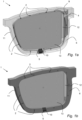
- Figure 1a shows an eye tracking device 1 integrated into a frame 11 of a pair of glasses. Only one of the frame for the right eye is shown.
- the eye tracking device comprises one or more illuminators 2, each illuminator 2 comprising a light emitting side 3, and each illuminator being connected to a first circuitry carrier 4.
- An imaging module 5 is connected to a second circuitry carrier 9 and the image module 5 comprises optical arrangement 10.
- the plurality of illuminators 2, the imaging module 5 and the circuitry carriers 4, 9 are embedded without gaps in a first material 6.
- the first material comprises openings 7 such that at least one of the light emitting sides of the illuminators and viewing portion 10 of the optical arrangement of the imaging module 5 are not covered by the first material 6.
- the first material 6 is transparent.
- All illuminators 2 are in this embodiment side emitting and connected to a single first circuitry carrier 4.
- the first circuitry carrier 4 and/or the second circuit carrier 9 may be a Printed Circuit Board PCB or a 3D molded interconnect devices 3D-MIDs.
- Figure 1b shows the same eye tracking device 1 integrated into a frame 11 of a pair of glasses as in Figure 1a where the first material 6 is non-transparent, at least to visible light. It could however be transparent for light from illuminators irradiating in NIR. In cases where the frame of the glasses has no openings, the first material 6 may be transparent for light from illuminators irradiating in NIR but non-transparent for visible light. If the openings 7 are filled with the second material, the second material must be transparent for light from illuminators. In that case the transparent properties of the first material are only important if the openings also should work as apertures for the illuminator light.
- the imaging module 5 in the embodiment of Figures 1a and 1b is a camera, but it could be a lens-less camera or any other image module capable of capturing the image of reflected illuminator(s) 2 in the eye of a user.
- the second circuitry carrier 9 in Figure 1a could in another embodiment (not shown) be an integral part of the first circuitry carrier 4.
- Figure 2 is a schematic view of how the openings of the first material 6 are filled with a second material 8 that is transparent for the light of the illuminators.
- the first material is in this embodiment non-transparent to the illuminator light to shield and define possible illumination angles of the illuminator 2.
- the opening 7 thus form an aperture to limit illuminator light emitting angles. This is especially important for VR applications.
- the illuminator is a LED.
- the illuminator could however be a laser, an incandescent lamp, a fluorescent material or any other light source suitable to fit into the device.
- the illuminators are Near Infrared (NIR) illuminators to not be visible to the user and the image module thereby has to be able to capture images in NIR images.
- NIR Near Infrared
- the second material 8 is an optical arrangement functioning as a window for the LED.
- optical arrangement built up by the second material 8 can be lens-shaped or shaped as a Fresnel lens.
- Figure 3 shows an embodiment without an optical arrangement or second material.
- the illuminator is a LED having its illuminating side 3 un-covered towards the environment.
- the LED top material is the preferably durable as e.g. PMMA. If softer LED top material is used as silico or epoxy the embodiment of Figure 2 is preferred where the LED is covered by the second material 8.
- Figure 4 illustrates a method for manufacturing an eye tracking device according to the invention, comprising the steps S1 providing a plurality of illuminator, each illuminator comprising a light emitting side, and each illuminator being connected to a first circuitry carrier, S2 providing an imaging module connected to a second circuitry carrier, the imaging module comprising a lens for capturing images of an eye, S3 embedding the plurality of illuminators, the imaging module and the circuitry carriers without gaps in a first material, wherein the first material comprises openings such that the light emitting sides of the illuminators and the imaging module lens are not covered by first material.
- the embodiment further comprises the step of S4 filling at least one of the openings of the first material with a second material that is transparent for the light of the illuminator.
- the step of embedding S3 comprises: S3a providing a first mold, S3b placing the first circuitry carrier and second circuitry carrier in the first mold, S3c filling the empty space of the first mold with the first material.
- Figure 5 illustrates another embodiment of a method for manufacturing an eye tracking device, comprising the steps S1 providing a plurality of illuminator, each illuminator comprising a light emitting side, and each illuminator being connected to a first circuitry carrier, S2 providing an imaging module connected to a second circuitry carrier, the imaging module comprising a lens for capturing images of an eye, S3 embedding the plurality of illuminators, the imaging module and the circuitry carriers without gaps in a first material, wherein the first material comprises openings such that the light emitting sides of the illuminators and the imaging module lens are not covered by first material.
- the step of embedding comprises S3e providing a second mold with empty spaces aligned with the light emitting sides of the illuminators and the viewing portion of the imaging module, S3f placing the first circuitry carrier and second circuitry carrier to the mold, S3g filling the second mold with the second material, such that at least the light emitting sides of the illuminators and the viewing portion of the imaging module are embedded in second material, S3h providing a first mold, S3i placing the first circuitry carrier and second circuitry carrier in the first mold, S3j filling the empty space of the first mold with the first material.
- the second material may be shaped to a lens, a Fresnel lens or any other light guiding structure.
- the surfaces may be polished to enhance optical properties or remove unwanted material in a manufacturing step.
Landscapes
- Physics & Mathematics (AREA)
- Engineering & Computer Science (AREA)
- General Physics & Mathematics (AREA)
- Optics & Photonics (AREA)
- General Engineering & Computer Science (AREA)
- Theoretical Computer Science (AREA)
- Health & Medical Sciences (AREA)
- Human Computer Interaction (AREA)
- Ophthalmology & Optometry (AREA)
- Acoustics & Sound (AREA)
- General Health & Medical Sciences (AREA)
- Otolaryngology (AREA)
- Studio Devices (AREA)
- Non-Portable Lighting Devices Or Systems Thereof (AREA)
Description
- The present invention relates to a device for eye tracking and a method for manufacturing an eye tracking device. More specifically, the disclosure relates to a device with one or more illuminators according to
claim 1 and methods according to the introductory parts ofclaims 12 and 16. - The illumination solutions in eye tracking devices are in an early stage of development. Many solutions are more or less development kits that are very simple. For device in glasses mechanical carrier rings and a flexible PCB with a number of Light Emitting Diodes (LED) are usually provided. The ring holds the LEDs in the correct position and angles them towards the eye of the user. The flex PCB is attached to the ring with a glue.
- More advanced device types use several mechanical plastic parts and one flex PCB. One part may be used for mounting the flex, called Carrier. Another NIR transparent part is used to cover and protect the LEDs on the flex, called LED Cover. Preferably this part is opaque to visible light to make it more attractive esthetically.
- The LED cover needs to have good optical properties and there are some design challenges. It is important that it doesn't act like a light guide and it should not cause the light to illuminate the eye though different optical paths. There are tough tolerances on the mechanical parts and assembly to ensure good optical performance and also good esthetical fit. The LED placement have very tight tolerances due to that offset can create either stray light or significantly diminish illumination level and loss of the glint.
- In both cases the LED flex can be angled to increase efficiency and also reduce stray light but this makes the assembly process more difficult, possibly requiring human based assembly which increases cost and lowers yield.
-
US 2015/0061995 A1 discloses a portable eye tracker including a frame, at least one optics holding member, a movement sensor, and a control unit. The at least one optics holding member includes at least one illuminator to illuminate the face of a user. - There is thus a need for solutions that make the assembly easier for large volumes providing precise tolerances. It is also a desire in the industry to enable smaller and more advanced form factors as the eye tracking devices are integrated in small structures as frames for glasses etc. A further problem is that previous solutions have gap between plastic parts causing problems with stray light and imprecise optical properties. Gaps in the assembly are also not esthetically attractive. Previous solutions are also more fragile as glued or mechanically joined parts break easily.
- It is an object to mitigate, alleviate or eliminate one or more of the above-identified deficiencies in the art and disadvantages singly or in any combination and solve at least the above mentioned problem.
- According to a first aspect there is provided an eye tracking device according to
claim 1. This solution provides smaller devices as the assembly is easier to automate. The assembly is also more precise providing less variations in the manufacturing. This solution also provides an eye tracking device that is free from gaps enhancing optical performance and provides better looking and more robust devices. If the first material is transparent to the radiation from the illuminators the illuminators and optionally also the imaging module may be embedded in the first material. - If the first material is not transparent to the irradiation from the illuminators, openings for the illuminators and/or the imaging module have to be present.
- According to some embodiments at least one of the openings of the first material are filled with a second material that is transparent for the light of the illuminators. In this way an integrated window can be created for the illuminator light source and/or imaging module.
- According to some embodiments, the openings are formed as apertures to limit illuminator light emitting angles. This is advantageous in VR applications so that the illuminators do not disturb the eye image due to light going into the lens creating stray light that obfuscate the eye in the image captured by the imaging module.
- According to some embodiments the first material is non-transparent to the illuminator light to stop light from the illuminator to propagate in certain angles. The non-transparent first material also provides a frame for the circuit carrier that visually hides the circuits from the user of the device providing a more attractive design.
- According to some embodiments at least the first material is shaped in the form of one of the frames of a pair of glasses so as to provide a device usable for Augmented Reality (AR) applications or Virtual Reality (VR) applications. According to some embodiments all illuminators are connected to a single first circuitry carrier so as to minimize the number of components. According to some embodiments the second circuitry carrier is an integral part of the first circuitry carrier so as to further minimize the number of components of the device.
- According to some embodiments the first circuitry carrier and/or the second circuitry carrier is a Printed Circuit Board, PCB, or a 3D molded interconnect devices, 3D-MIDs. According to some embodiments the imaging module is a camera or a lens-less camera or any other imaging device.
- According to some embodiments the illuminators are front emitting to maximize light emittance in the frontal direction of the illuminators or side emitting to avoid light emittance in certain directions from the illuminators. According to some embodiments the illuminator is a radiation source comprised in the group of: a LED, a laser, an incandescent lamp and a fluorescent material. The smallest, most robust, most energy efficient and cheapest solution is preferably used. A LED is therefore preferred in the current industry but developments in light sources may call for another radiation source. According to some embodiments the illuminators are Near Infrared (NIR) illuminators. This is advantageous as NIR radiation is not visible to the human eye.
- According to some embodiments the first circuitry carrier and/or the second circuitry carrier is flexible to make the automated assembly easier or to enable a flexible design of the eye tracking device.
- According to some embodiments the second material is an optical arrangement so as to enhance the optical properties in a certain way. It could e.g. be a lens shape to form a positive or negative lens. It may also be a pattern forming a Fresnel lens or any other similar shape giving a lens effect.
- According to some embodiments the first material is poly(methyl methacrylate), PMMA, polycarbonate, PC, Zeonex or acrylonitrile butadiene styrene, ABS with or without added pigments that are transparent to NIR, and/or the second material is PMMA, PC, Zeonex or ABS with added pigments that are non-transparent to NIR.
- Further aspect of the present invention can be described as an eye tracking device comprising one or more illuminators, each illuminator comprising a light emitting side, and each illuminator being connected to a first circuitry carrier, an imaging module connected to a second circuitry carrier, the imaging module comprising optical arrangements, wherein the plurality of illuminators, the imaging module and the circuitry carriers are embedded without gaps in a first material, wherein the first material is transparent to IR light but non-transparent to visible light.
- According to a second aspect there is provided a method for manufacturing an eye tracking device according to
claim 12. Increased yield in production may be achieved due to fewer and simpler steps then in the prior art manufacturing with often manual assembly of mechanical parts. The manufacturing method also enables that it becomes simple to change the design of the eye tracking device using the same PCBs and image module. - According to some embodiments the method further comprises the step of filling at least one of the openings of the first material with a second material that is transparent for the light of the illuminator.
- According to some embodiments the step of embedding comprises: providing a first mold, placing the first circuitry carrier and second circuitry carrier in the first mold, filling the empty space of the first mold with the first material. This is a process that is suitable for automated assembly.
- According to some embodiments the mold comprises first structures for preventing the first material to cover the light emitting side of the illuminators and a second structure for preventing the first material to cover the imaging module. In that way the first material may be molded without covering the illuminators and imaging module. The second material may then be molded into the empty openings in the first material being a consequence of the illuminators and imaging module previously being covered by the first structures and the second structures. The mold may comprise alignment features for aligning the first structures and the second structure with the illuminators and imaging module, respectively. By exactly fixating the first circuitry carrier and second circuitry carrier in the first mold a precise fit is always accomplished so that the components are always placed in the same exact way for every manufactured device.
- According to some embodiments, the step of embedding comprises: providing a second mold with empty spaces aligned with the light emitting sides of the illuminators and the optical arrangement of the imaging module, placing the first circuitry carrier and second circuitry carrier to the second mold, filling the second mold with the second material, such that at least the light emitting sides of the illuminators and the viewing portion of the imaging module are embedded in second material, providing a first mold, placing the first circuitry carrier and second circuitry carrier in the first mold, filling the empty space of the first mold with the first material such that the plurality of illuminators, the imaging module, and the circuitry carriers are embedded without gaps in the first material. In this way the second material, intended to be transparent window to the illuminators, is applied first covering/encapsulating the illuminators and/or the image module. In that way there is no risk of by mistake covering the illuminator and/or image module with the first material that is non-transparent for the radiation from the illuminator(s).
- According to a third aspect there is provided a method for manufacturing an eye tracking device according to the device described above, wherein the first material and/or the second material is placed using a 3D-printer.
- According to some embodiments, the method further comprises the step of polishing the surface of the illuminators and/or imaging module so as to remove non-transparent material from illuminator surface and/or accomplish a polished optically equal surface.
- Effects and features of the second and third aspects are largely analogous to those described above in connection with the first aspect. Embodiments mentioned in relation to the first aspect are largely compatible with the second and third aspects.
- A further scope of applicability of the present invention will become apparent from the detailed description given below. However, it should be understood that the detailed description and specific examples are given by way of illustration only, since various changes and modifications within the scope of the invention will become apparent to those skilled in the art from the appended claims.
- Hence, it is to be understood that this invention is not limited to the particular component parts of the device described or steps of the methods described as such device and method may vary. It is also to be understood that the terminology used herein is for purpose of describing particular embodiments only, and is not intended to be limiting. It must be noted that, as used in the specification and the appended claim, the articles "a", "an", "the", and "said" are intended to mean that there are one or more of the elements unless the context clearly dictates otherwise. Thus, for example, reference to "a unit" or "the unit" may include several devices, and the like. Furthermore, the words "comprising", "including", "containing" and similar wordings does not exclude other elements or steps.
- The above objects, as well as additional objects, features and advantages of the present invention, will be more fully appreciated by reference to the following illustrative and non-limiting detailed description of preferred embodiments of the present invention, when taken in conjunction with the accompanying drawings, wherein:
-
Fig. 1a is a perspective view of an eye tracking device integrated in a frame of a pair of glasses where the first material is transparent. -
Fig. 1b is a perspective view of an eye tracking device integrated in a frame of a pair of glasses where the first material is non-transparent. -
Fig. 2 is a schematic view of an over-molded illuminator LED with first material and second material. -
Fig. 3 is a schematic view of an over-molded illuminator LED with only first material. -
Fig. 4 is a box diagram showing a first method for manufacturing an eye tracking device. -
Fig. 5 is a box diagram showing a second method for manufacturing an eye tracking device. - The present invention will now be described more fully hereinafter with reference to the accompanying drawings, in which currently preferred embodiments of the invention are shown.
-
Figure 1a shows aneye tracking device 1 integrated into aframe 11 of a pair of glasses. Only one of the frame for the right eye is shown. The eye tracking device comprises one ormore illuminators 2, eachilluminator 2 comprising alight emitting side 3, and each illuminator being connected to afirst circuitry carrier 4. Animaging module 5 is connected to asecond circuitry carrier 9 and theimage module 5 comprisesoptical arrangement 10. The plurality ofilluminators 2, theimaging module 5 and thecircuitry carriers first material 6. The first material comprisesopenings 7 such that at least one of the light emitting sides of the illuminators andviewing portion 10 of the optical arrangement of theimaging module 5 are not covered by thefirst material 6. InFigure 1a thefirst material 6 is transparent. Allilluminators 2 are in this embodiment side emitting and connected to a singlefirst circuitry carrier 4. Thefirst circuitry carrier 4 and/or thesecond circuit carrier 9 may be a Printed Circuit Board PCB or a 3D molded interconnect devices 3D-MIDs. -
Figure 1b shows the sameeye tracking device 1 integrated into aframe 11 of a pair of glasses as inFigure 1a where thefirst material 6 is non-transparent, at least to visible light. It could however be transparent for light from illuminators irradiating in NIR. In cases where the frame of the glasses has no openings, thefirst material 6 may be transparent for light from illuminators irradiating in NIR but non-transparent for visible light. If theopenings 7 are filled with the second material, the second material must be transparent for light from illuminators. In that case the transparent properties of the first material are only important if the openings also should work as apertures for the illuminator light. - The
imaging module 5 in the embodiment ofFigures 1a and 1b is a camera, but it could be a lens-less camera or any other image module capable of capturing the image of reflected illuminator(s) 2 in the eye of a user. - The
second circuitry carrier 9 inFigure 1a could in another embodiment (not shown) be an integral part of thefirst circuitry carrier 4. -
Figure 2 is a schematic view of how the openings of thefirst material 6 are filled with asecond material 8 that is transparent for the light of the illuminators. The first material is in this embodiment non-transparent to the illuminator light to shield and define possible illumination angles of theilluminator 2. Theopening 7 thus form an aperture to limit illuminator light emitting angles. This is especially important for VR applications. - In
Figures 1a, 1b ,2 and 3 the illuminator is a LED. The illuminator could however be a laser, an incandescent lamp, a fluorescent material or any other light source suitable to fit into the device. The illuminators are Near Infrared (NIR) illuminators to not be visible to the user and the image module thereby has to be able to capture images in NIR images. - In
Figure 2 thesecond material 8 is an optical arrangement functioning as a window for the LED. According to a different embodiment optical arrangement built up by thesecond material 8 can be lens-shaped or shaped as a Fresnel lens. -
Figure 3 shows an embodiment without an optical arrangement or second material. The illuminator is a LED having its illuminatingside 3 un-covered towards the environment. The LED top material is the preferably durable as e.g. PMMA. If softer LED top material is used as silico or epoxy the embodiment ofFigure 2 is preferred where the LED is covered by thesecond material 8. -
Figure 4 illustrates a method for manufacturing an eye tracking device according to the invention, comprising the steps S1 providing a plurality of illuminator, each illuminator comprising a light emitting side, and each illuminator being connected to a first circuitry carrier, S2 providing an imaging module connected to a second circuitry carrier, the imaging module comprising a lens for capturing images of an eye, S3 embedding the plurality of illuminators, the imaging module and the circuitry carriers without gaps in a first material, wherein the first material comprises openings such that the light emitting sides of the illuminators and the imaging module lens are not covered by first material. The embodiment further comprises the step of S4 filling at least one of the openings of the first material with a second material that is transparent for the light of the illuminator. The step of embedding S3 comprises:
S3a providing a first mold, S3b placing the first circuitry carrier and second circuitry carrier in the first mold, S3c filling the empty space of the first mold with the first material. -
Figure 5 illustrates another embodiment of a method for manufacturing an eye tracking device, comprising the steps S1 providing a plurality of illuminator, each illuminator comprising a light emitting side, and each illuminator being connected to a first circuitry carrier, S2 providing an imaging module connected to a second circuitry carrier, the imaging module comprising a lens for capturing images of an eye, S3 embedding the plurality of illuminators, the imaging module and the circuitry carriers without gaps in a first material, wherein the first material comprises openings such that the light emitting sides of the illuminators and the imaging module lens are not covered by first material. The step of embedding comprises S3e providing a second mold with empty spaces aligned with the light emitting sides of the illuminators and the viewing portion of the imaging module, S3f placing the first circuitry carrier and second circuitry carrier to the mold, S3g filling the second mold with the second material, such that at least the light emitting sides of the illuminators and the viewing portion of the imaging module are embedded in second material, S3h providing a first mold, S3i placing the first circuitry carrier and second circuitry carrier in the first mold, S3j filling the empty space of the first mold with the first material. - The person skilled in the art realizes that the present invention by no means is limited to the preferred embodiments described above. On the contrary, many modifications and variations are possible within the scope of the appended claims. For example, even though not shown in the Figures, the second material may be shaped to a lens, a Fresnel lens or any other light guiding structure. The surfaces may be polished to enhance optical properties or remove unwanted material in a manufacturing step.
- Additionally, variations to the disclosed embodiments can be understood and effected by the skilled person in practicing the claimed invention, from a study of the drawings, the disclosure, and the appended claims, but within scope of the appended claims.
Claims (17)
- An eye tracking device (1) comprisingone or more illuminators (2), each illuminator (2) comprising a light emitting side (3), and each illuminator (2) being connected to a first circuitry carrier (4),an imaging module (5) connected to a second circuitry carrier (9), the imaging module (5) comprising optical arrangements,characterised in that the plurality of illuminators (2), the imaging module (5) and the circuitry carriers (4, 9) are embedded without gaps in a first material (6),wherein, if the first material (6) is not transparent to the irradiation from the illuminators (2) and/or the irradiation detected by the imaging module (5), the first material (6) comprises openings (7) such that the light emitting sides (3) of the illuminators (2) and/or the optical arrangements of the imaging module (5) are not covered by first material (6).
- The eye tracking device (1) according to claim 1, wherein at least one of the openings (7) of the first material (6) are filled with a second material (8) that is transparent for the light of the illuminators (2).
- The eye tracking device (1) according to claim 1 or claim 2, wherein the openings (7) are formed as apertures to limit illuminator light emitting angles.
- The eye tracking device (1) according to any one of the preceding claims,wherein the first material (6) is non-transparent to the illuminator light, and/orwherein at least the first material (6) is shaped in the form of one of the frames (11) of a pair of glasses, and/or wherein the first material (6) is poly(methyl methacrylate), PMMA, polycarbonate, PC, Zeonex or acrylonitrile butadiene styrene, ABS, with or without added pigments that are transparent to near-infrared, NIR.
- The eye tracking device (1) according to any one of the preceding claims,
wherein all illuminators (2) are connected to a single first circuitry carrier (4), and/or wherein the second circuitry carrier (9) is an integral part of the first circuitry carrier (4). - The eye tracking device (1) according to any one of the preceding claims,
wherein the first circuitry carrier (4) and/or the second circuit carrier (9) are Printed Circuit Boards, PCBs, or 3D molded interconnect devices, 3D-MIDs. - The eye tracking device (1) according to any one of the preceding claims, wherein the imaging module (5) is a module comprised in the group of: a camera, a lens-less camera.
- The eye tracking device (1) according to any one of the preceding claims, wherein the illuminators (2) are front emitting to maximize light emittance in the frontal direction of the illuminators (2) or side emitting to avoid light emittance in certain directions from the illuminators (2), and/or wherein the illuminator (2) is a radiation source comprised in the group of: a LED, a laser, an incandescent lamp and a fluorescent material, and/or wherein the illuminators (2) are Near Infrared, NIR, illuminators.
- The eye tracking device (1) according to any one of the preceding claims, wherein the first circuitry carrier (4) and/or the second circuitry carrier (9) is flexible.
- The eye tracking device (1) according to any of the preceding claims, wherein the first material (6) is transparent to IR light but non-transparent to visible light.
- The eye tracking device (1) according to any one of the preceding claims,
wherein the optical arrangement is a Fresnel lens. - A method for manufacturing an eye tracking device (1), comprising the steps of:providing (S1) a plurality of illuminators (2), each illuminator (2) comprising a light emitting side (3), and each illuminator (2) being connected to a first circuitry carrier (4), andproviding (S2) an imaging module (5) connected to a second circuitry carrier (9), the imaging module (5) comprising an optical arrangement for capturing images of an eye,characterised by further comprising the step of embedding (S3) the plurality of illuminators (2), the imaging module (5) and the circuitry carriers (4, 9) without gaps in a first material (6), wherein, if the first material (6) is not transparent to the irradiation from the illuminators (2) and/or the irradiation detected by the imaging module (5), the first material (6) comprises openings (7) such that the light emitting sides (3) of the illuminators (2) and/or the optical arrangement of the imaging module (5) are not covered by first material (6).
- The method for manufacturing an eye tracking device (1) according to claim 12, further comprising the step of filling (S4) at least one of the openings (7) of the first material (6) with a second material (8) that is transparent for the light of the illuminator (2).
- The method for manufacturing an eye tracking device (1) according to claim 12, wherein the step of embedding (S3) comprises:providing (S3a) a first mold,placing (S3b) the first circuitry carrier (4) and second circuitry carrier (9) in the first mold,filling (S3c) the empty space of the first mold with the first material (6), wherein the mold preferably comprises first structures for preventing the first material (6) from covering the light emitting side (3) of the illuminators (2) and a second structure for preventing the first material (6) from covering the imaging module (5) and wherein the first mold preferably comprises alignment features for aligning the first structures and the second structure with the illuminators (2) and imaging module (5), respectively.
- The method for manufacturing an eye tracking device (1) according to claim 12, wherein the step of embedding (S3) comprises:providing (S3e) a second mold with empty spaces aligned with the light emitting sides (3) of the illuminators (2) and the optical arrangement of the imaging module (5),placing (S3f) the first circuitry carrier (4) and second circuitry carrier (9) to the second mold,filling (S3g) the second mold with a second material (8), such that at least the light emitting sides (3) of the illuminators (2) and the viewing portion of the imaging module (5) are embedded in second material (8),providing (S3h) a first mold,placing (S3i) the first circuitry carrier (4) and second circuitry carrier (9) in the first mold, filling (S3j) the empty space of the first mold with the first material (6) such that the plurality of illuminators (2), the imaging module (5), and the circuitry carriers (4, 9) are embedded without gaps in the first material (6).
- A method for manufacturing an eye tracking device (1) according to any of claims 1 to 11, wherein the first material (6) and/or the second material (8) is placed using a 3D-printer.
- The method for manufacturing an eye tracking device (1) according to any one of claims 12 to 16, further comprising the step of polishing the surface of the illuminators (2) and/or imaging module (5) so as to remove non-transparent material from illuminator surface and/or accomplish a polished optically equal surface.
Applications Claiming Priority (1)
| Application Number | Priority Date | Filing Date | Title |
|---|---|---|---|
| SE1850724 | 2018-06-13 |
Publications (2)
| Publication Number | Publication Date |
|---|---|
| EP3582077A1 EP3582077A1 (en) | 2019-12-18 |
| EP3582077B1 true EP3582077B1 (en) | 2024-10-30 |
Family
ID=66999553
Family Applications (1)
| Application Number | Title | Priority Date | Filing Date |
|---|---|---|---|
| EP19179462.7A Active EP3582077B1 (en) | 2018-06-13 | 2019-06-11 | Eye tracking device and method for manufacturing an eye tracking device |
Country Status (3)
| Country | Link |
|---|---|
| US (2) | US11256327B2 (en) |
| EP (1) | EP3582077B1 (en) |
| CN (1) | CN110596889A (en) |
Families Citing this family (8)
| Publication number | Priority date | Publication date | Assignee | Title |
|---|---|---|---|---|
| CN111417257A (en) * | 2020-04-28 | 2020-07-14 | 南昌欧菲显示科技有限公司 | Lighting modules and AR glasses |
| WO2021217418A1 (en) * | 2020-04-28 | 2021-11-04 | 南昌欧菲显示科技有限公司 | Light-emitting module and ar glasses |
| CN111783660B (en) * | 2020-07-01 | 2023-11-10 | 业成科技(成都)有限公司 | Eye movement tracking device and electronic device using same |
| US11867915B2 (en) * | 2021-03-31 | 2024-01-09 | Microsoft Technology Licensing, Llc | Head mounted display with obscured light emitting diodes |
| US12339443B2 (en) * | 2022-03-31 | 2025-06-24 | Tobii Ab | Assembly for an eye tracking system and a corresponding head-mounted device utilizing the same |
| SE546866C2 (en) * | 2023-03-02 | 2025-03-04 | Tobii Ab | Eye tracking glasses |
| WO2025012901A1 (en) * | 2023-07-09 | 2025-01-16 | Immersix Ltd | Gaze tracking by coaxial light imaging of a retina |
| TWI878978B (en) * | 2023-07-13 | 2025-04-01 | 大陸商榮諭科技(成都)有限公司 | The method of preparing eye-tracking glasses |
Family Cites Families (42)
| Publication number | Priority date | Publication date | Assignee | Title |
|---|---|---|---|---|
| DE3789731T2 (en) | 1986-06-20 | 1994-08-18 | Hitachi Ltd | Digital video signal processor. |
| DE69721537T2 (en) * | 1996-06-06 | 2004-04-01 | British Telecommunications P.L.C. | IDENTIFICATION OF PERSONS |
| US6299308B1 (en) | 1999-04-02 | 2001-10-09 | Cybernet Systems Corporation | Low-cost non-imaging eye tracker system for computer control |
| CN100380924C (en) * | 2002-07-18 | 2008-04-09 | 皇家飞利浦电子股份有限公司 | Camera module, holder for use in camera module, camera system and method of manufacturing camera module |
| US20070053179A1 (en) * | 2005-09-08 | 2007-03-08 | Pang Slew I | Low profile light source utilizing a flexible circuit carrier |
| FR2900475B1 (en) * | 2006-04-26 | 2008-10-31 | Essilor Int | DISPLAY COMPRISING A PAIR OF BINOCULAR GLASSES AND WITH A DEVICE FOR ADJUSTING THE IMAGE |
| DE102009008845B4 (en) * | 2009-02-13 | 2024-10-17 | Inventronics Gmbh | light module |
| US8398239B2 (en) | 2009-03-02 | 2013-03-19 | Honeywell International Inc. | Wearable eye tracking system |
| CN101930932A (en) * | 2009-06-22 | 2010-12-29 | 国格金属科技股份有限公司 | LED light-emitting module manufacturing method |
| CN201491400U (en) * | 2009-07-22 | 2010-05-26 | 广州兴森快捷电路科技有限公司 | Device used for metalization manufacturing of three dimensional printing plate |
| WO2011153112A2 (en) * | 2010-05-29 | 2011-12-08 | Wenyu Jiang | Systems, methods and apparatus for making and using eyeglasses with adaptive lens driven by gaze distance and low power gaze tracking |
| US8531355B2 (en) * | 2010-07-23 | 2013-09-10 | Gregory A. Maltz | Unitized, vision-controlled, wireless eyeglass transceiver |
| JP5879353B2 (en) * | 2010-10-07 | 2016-03-08 | 株式会社ソニー・コンピュータエンタテインメント | Head position and orientation tracking |
| EP2499964B1 (en) * | 2011-03-18 | 2015-04-15 | SensoMotoric Instruments Gesellschaft für innovative Sensorik mbH | Optical measuring device and system |
| US9087471B2 (en) * | 2011-11-04 | 2015-07-21 | Google Inc. | Adaptive brightness control of head mounted display |
| NZ719204A (en) * | 2012-01-24 | 2017-11-24 | Univ Arizona | Compact eye-tracked head-mounted display |
| EP2929413B1 (en) * | 2012-12-06 | 2020-06-03 | Google LLC | Eye tracking wearable devices and methods for use |
| KR101968455B1 (en) * | 2013-09-03 | 2019-04-11 | 토비 에이비 | Portable eye tracking device |
| CN105518514B (en) * | 2013-09-06 | 2019-07-05 | 3M创新有限公司 | Head-mounted display with eyes tracking |
| CN204496106U (en) * | 2013-10-11 | 2015-07-22 | 天空激光二极管有限公司 | Wearable device |
| EP2886041A1 (en) * | 2013-12-17 | 2015-06-24 | ESSILOR INTERNATIONAL (Compagnie Générale d'Optique) | Method for calibrating a head-mounted eye tracking device |
| US9459451B2 (en) * | 2013-12-26 | 2016-10-04 | Microsoft Technology Licensing, Llc | Eye tracking apparatus, method and system |
| US10690945B2 (en) * | 2014-02-18 | 2020-06-23 | Essilor International | Method for optimizing an optical lens equipment for a wearer |
| US9280693B2 (en) * | 2014-05-13 | 2016-03-08 | Hand Held Products, Inc. | Indicia-reader housing with an integrated optical structure |
| CA2949250C (en) * | 2014-05-28 | 2024-02-20 | Inoptec Limited Zweigniederlassung Deutschland | Electronic spectacles |
| US9422993B2 (en) | 2014-07-28 | 2016-08-23 | Shimano Inc. | Rotor cover, rotor cooling apparatus, and temperature-level indicator |
| US10108017B2 (en) * | 2015-01-20 | 2018-10-23 | Microsoft Technology Licensing, Llc | Carbon nanoparticle infused optical mount |
| US9779512B2 (en) * | 2015-01-29 | 2017-10-03 | Microsoft Technology Licensing, Llc | Automatic generation of virtual materials from real-world materials |
| EP3259632A4 (en) * | 2015-02-17 | 2018-02-28 | Osterhout Group, Inc. | See-through computer display systems |
| EP3112922A1 (en) | 2015-06-30 | 2017-01-04 | Thomson Licensing | A gaze tracking device and a head mounted device embedding said gaze tracking device |
| JP6686505B2 (en) * | 2016-02-15 | 2020-04-22 | セイコーエプソン株式会社 | Head-mounted image display device |
| CN106406509B (en) * | 2016-05-16 | 2023-08-01 | 上海青研科技有限公司 | Head-mounted eye-control virtual reality equipment |
| CN106644085A (en) | 2016-09-21 | 2017-05-10 | 广州视源电子科技股份有限公司 | Temperature measuring method and infrared thermometer |
| CN109923499B (en) | 2016-09-27 | 2022-07-29 | 托比股份公司 | Portable eye tracking device |
| CN106501941B (en) * | 2016-12-15 | 2019-07-16 | 浙江大华技术股份有限公司 | A kind of head-wearing display device |
| WO2018122677A1 (en) * | 2016-12-27 | 2018-07-05 | Semiconductor Energy Laboratory Co., Ltd. | Light-emitting element, light-emitting device, electronic device, and lighting device |
| US10419701B2 (en) * | 2017-06-26 | 2019-09-17 | Facebook Technologies, Llc | Digital pixel image sensor |
| EP3485799B9 (en) * | 2017-11-16 | 2022-02-16 | Aptiv Technologies Limited | Eye tracking device |
| KR102476757B1 (en) * | 2017-12-21 | 2022-12-09 | 삼성전자주식회사 | Device and method to detect reflection |
| KR20190085368A (en) * | 2018-01-10 | 2019-07-18 | 삼성전자주식회사 | Folding-type wearable electronic device with optical transfering member transfer to transparent member from projector |
| WO2020010271A1 (en) * | 2018-07-05 | 2020-01-09 | Magic Leap, Inc. | Waveguide-based illumination for head mounted display system |
| CN208805638U (en) * | 2018-07-30 | 2019-04-30 | 成都理想境界科技有限公司 | A kind of intelligent glasses and frame |
-
2019
- 2019-06-11 CN CN201910501692.0A patent/CN110596889A/en active Pending
- 2019-06-11 EP EP19179462.7A patent/EP3582077B1/en active Active
- 2019-06-13 US US16/440,074 patent/US11256327B2/en active Active
-
2022
- 2022-02-22 US US17/677,531 patent/US11687156B2/en active Active
Also Published As
| Publication number | Publication date |
|---|---|
| US11256327B2 (en) | 2022-02-22 |
| US20200348753A1 (en) | 2020-11-05 |
| US20220179487A1 (en) | 2022-06-09 |
| CN110596889A (en) | 2019-12-20 |
| EP3582077A1 (en) | 2019-12-18 |
| US11687156B2 (en) | 2023-06-27 |
Similar Documents
| Publication | Publication Date | Title |
|---|---|---|
| EP3582077B1 (en) | Eye tracking device and method for manufacturing an eye tracking device | |
| CN208654686U (en) | Portable electronic device | |
| KR101346867B1 (en) | Input device | |
| EP2779807A1 (en) | Optic for a light source | |
| KR101707861B1 (en) | Apparatus for Taking Close-Up Picture Using Mobile Terminal Equipped with Camera, and External-Optical Device thereof | |
| US9251397B2 (en) | Fingerprint image capturing device and fingerprint image capturing module thereof | |
| EP3006998B1 (en) | Image pickup apparatus | |
| CN109271057A (en) | Display module and electronic device | |
| CN109698894A (en) | Photosensory assembly and camera module based on metallic support | |
| CN106164831A (en) | Location input device and touch panel | |
| KR20160030156A (en) | System and method for aligning two work pieces with a vision system in the presence of occlusion | |
| CN108200238A (en) | Electronic device | |
| US7789519B2 (en) | Illuminated display window for LED and/or LC displays | |
| US8950066B2 (en) | Method for manufacturing light emitting diode module | |
| CN103455209B (en) | Optical sensing apparatus | |
| CN202938241U (en) | Thin light guide structure using LED flash on portable electronic devices | |
| EP3470917B1 (en) | Imaging device | |
| US11697257B2 (en) | Method for mounting functional elements in a lens | |
| EP3001671A1 (en) | Image pickup apparatus | |
| CN110426807A (en) | Lens module | |
| CN103576259B (en) | The joints of optical fibre and assemble method | |
| KR20130092433A (en) | Component module | |
| JP6620320B2 (en) | Reader | |
| US20140174629A1 (en) | Method for manufacturing light emitting diode module | |
| CN106022184A (en) | Illumination device and system |
Legal Events
| Date | Code | Title | Description |
|---|---|---|---|
| PUAI | Public reference made under article 153(3) epc to a published international application that has entered the european phase |
Free format text: ORIGINAL CODE: 0009012 |
|
| STAA | Information on the status of an ep patent application or granted ep patent |
Free format text: STATUS: THE APPLICATION HAS BEEN PUBLISHED |
|
| AK | Designated contracting states |
Kind code of ref document: A1 Designated state(s): AL AT BE BG CH CY CZ DE DK EE ES FI FR GB GR HR HU IE IS IT LI LT LU LV MC MK MT NL NO PL PT RO RS SE SI SK SM TR |
|
| AX | Request for extension of the european patent |
Extension state: BA ME |
|
| STAA | Information on the status of an ep patent application or granted ep patent |
Free format text: STATUS: REQUEST FOR EXAMINATION WAS MADE |
|
| 17P | Request for examination filed |
Effective date: 20200616 |
|
| RBV | Designated contracting states (corrected) |
Designated state(s): AL AT BE BG CH CY CZ DE DK EE ES FI FR GB GR HR HU IE IS IT LI LT LU LV MC MK MT NL NO PL PT RO RS SE SI SK SM TR |
|
| STAA | Information on the status of an ep patent application or granted ep patent |
Free format text: STATUS: EXAMINATION IS IN PROGRESS |
|
| 17Q | First examination report despatched |
Effective date: 20211202 |
|
| RAP3 | Party data changed (applicant data changed or rights of an application transferred) |
Owner name: TOBII AB |
|
| RAP3 | Party data changed (applicant data changed or rights of an application transferred) |
Owner name: TOBII AB |
|
| GRAP | Despatch of communication of intention to grant a patent |
Free format text: ORIGINAL CODE: EPIDOSNIGR1 |
|
| STAA | Information on the status of an ep patent application or granted ep patent |
Free format text: STATUS: GRANT OF PATENT IS INTENDED |
|
| RIC1 | Information provided on ipc code assigned before grant |
Ipc: G02C 11/04 20060101ALI20240408BHEP Ipc: G02C 11/00 20060101ALI20240408BHEP Ipc: G02B 27/00 20060101ALI20240408BHEP Ipc: G02B 27/01 20060101ALI20240408BHEP Ipc: G06F 3/01 20060101AFI20240408BHEP |
|
| INTG | Intention to grant announced |
Effective date: 20240423 |
|
| GRAS | Grant fee paid |
Free format text: ORIGINAL CODE: EPIDOSNIGR3 |
|
| P01 | Opt-out of the competence of the unified patent court (upc) registered |
Free format text: CASE NUMBER: APP_39581/2024 Effective date: 20240703 |
|
| GRAA | (expected) grant |
Free format text: ORIGINAL CODE: 0009210 |
|
| STAA | Information on the status of an ep patent application or granted ep patent |
Free format text: STATUS: THE PATENT HAS BEEN GRANTED |
|
| AK | Designated contracting states |
Kind code of ref document: B1 Designated state(s): AL AT BE BG CH CY CZ DE DK EE ES FI FR GB GR HR HU IE IS IT LI LT LU LV MC MK MT NL NO PL PT RO RS SE SI SK SM TR |
|
| REG | Reference to a national code |
Ref country code: GB Ref legal event code: FG4D |
|
| REG | Reference to a national code |
Ref country code: CH Ref legal event code: EP |
|
| REG | Reference to a national code |
Ref country code: DE Ref legal event code: R096 Ref document number: 602019061030 Country of ref document: DE |
|
| REG | Reference to a national code |
Ref country code: IE Ref legal event code: FG4D |
|
| REG | Reference to a national code |
Ref country code: LT Ref legal event code: MG9D |
|
| REG | Reference to a national code |
Ref country code: NL Ref legal event code: MP Effective date: 20241030 |
|
| PG25 | Lapsed in a contracting state [announced via postgrant information from national office to epo] |
Ref country code: PT Free format text: LAPSE BECAUSE OF FAILURE TO SUBMIT A TRANSLATION OF THE DESCRIPTION OR TO PAY THE FEE WITHIN THE PRESCRIBED TIME-LIMIT Effective date: 20250228 Ref country code: HR Free format text: LAPSE BECAUSE OF FAILURE TO SUBMIT A TRANSLATION OF THE DESCRIPTION OR TO PAY THE FEE WITHIN THE PRESCRIBED TIME-LIMIT Effective date: 20241030 Ref country code: IS Free format text: LAPSE BECAUSE OF FAILURE TO SUBMIT A TRANSLATION OF THE DESCRIPTION OR TO PAY THE FEE WITHIN THE PRESCRIBED TIME-LIMIT Effective date: 20250228 |
|
| PG25 | Lapsed in a contracting state [announced via postgrant information from national office to epo] |
Ref country code: FI Free format text: LAPSE BECAUSE OF FAILURE TO SUBMIT A TRANSLATION OF THE DESCRIPTION OR TO PAY THE FEE WITHIN THE PRESCRIBED TIME-LIMIT Effective date: 20241030 Ref country code: NL Free format text: LAPSE BECAUSE OF FAILURE TO SUBMIT A TRANSLATION OF THE DESCRIPTION OR TO PAY THE FEE WITHIN THE PRESCRIBED TIME-LIMIT Effective date: 20241030 |
|
| REG | Reference to a national code |
Ref country code: AT Ref legal event code: MK05 Ref document number: 1737539 Country of ref document: AT Kind code of ref document: T Effective date: 20241030 |
|
| PG25 | Lapsed in a contracting state [announced via postgrant information from national office to epo] |
Ref country code: BG Free format text: LAPSE BECAUSE OF FAILURE TO SUBMIT A TRANSLATION OF THE DESCRIPTION OR TO PAY THE FEE WITHIN THE PRESCRIBED TIME-LIMIT Effective date: 20241030 |
|
| PG25 | Lapsed in a contracting state [announced via postgrant information from national office to epo] |
Ref country code: ES Free format text: LAPSE BECAUSE OF FAILURE TO SUBMIT A TRANSLATION OF THE DESCRIPTION OR TO PAY THE FEE WITHIN THE PRESCRIBED TIME-LIMIT Effective date: 20241030 |
|
| PG25 | Lapsed in a contracting state [announced via postgrant information from national office to epo] |
Ref country code: NO Free format text: LAPSE BECAUSE OF FAILURE TO SUBMIT A TRANSLATION OF THE DESCRIPTION OR TO PAY THE FEE WITHIN THE PRESCRIBED TIME-LIMIT Effective date: 20250130 |
|
| PG25 | Lapsed in a contracting state [announced via postgrant information from national office to epo] |
Ref country code: LV Free format text: LAPSE BECAUSE OF FAILURE TO SUBMIT A TRANSLATION OF THE DESCRIPTION OR TO PAY THE FEE WITHIN THE PRESCRIBED TIME-LIMIT Effective date: 20241030 Ref country code: GR Free format text: LAPSE BECAUSE OF FAILURE TO SUBMIT A TRANSLATION OF THE DESCRIPTION OR TO PAY THE FEE WITHIN THE PRESCRIBED TIME-LIMIT Effective date: 20250131 Ref country code: AT Free format text: LAPSE BECAUSE OF FAILURE TO SUBMIT A TRANSLATION OF THE DESCRIPTION OR TO PAY THE FEE WITHIN THE PRESCRIBED TIME-LIMIT Effective date: 20241030 |
|
| PG25 | Lapsed in a contracting state [announced via postgrant information from national office to epo] |
Ref country code: PL Free format text: LAPSE BECAUSE OF FAILURE TO SUBMIT A TRANSLATION OF THE DESCRIPTION OR TO PAY THE FEE WITHIN THE PRESCRIBED TIME-LIMIT Effective date: 20241030 |
|
| PG25 | Lapsed in a contracting state [announced via postgrant information from national office to epo] |
Ref country code: RS Free format text: LAPSE BECAUSE OF FAILURE TO SUBMIT A TRANSLATION OF THE DESCRIPTION OR TO PAY THE FEE WITHIN THE PRESCRIBED TIME-LIMIT Effective date: 20250130 |
|
| PG25 | Lapsed in a contracting state [announced via postgrant information from national office to epo] |
Ref country code: SM Free format text: LAPSE BECAUSE OF FAILURE TO SUBMIT A TRANSLATION OF THE DESCRIPTION OR TO PAY THE FEE WITHIN THE PRESCRIBED TIME-LIMIT Effective date: 20241030 |
|
| PGFP | Annual fee paid to national office [announced via postgrant information from national office to epo] |
Ref country code: DE Payment date: 20250617 Year of fee payment: 7 |
|
| PG25 | Lapsed in a contracting state [announced via postgrant information from national office to epo] |
Ref country code: DK Free format text: LAPSE BECAUSE OF FAILURE TO SUBMIT A TRANSLATION OF THE DESCRIPTION OR TO PAY THE FEE WITHIN THE PRESCRIBED TIME-LIMIT Effective date: 20241030 |
|
| PGFP | Annual fee paid to national office [announced via postgrant information from national office to epo] |
Ref country code: GB Payment date: 20250617 Year of fee payment: 7 |