EP3582011A1 - Information processing apparatus, method, program, lithography system, and manufacturing method of article - Google Patents
Information processing apparatus, method, program, lithography system, and manufacturing method of article Download PDFInfo
- Publication number
- EP3582011A1 EP3582011A1 EP19179437.9A EP19179437A EP3582011A1 EP 3582011 A1 EP3582011 A1 EP 3582011A1 EP 19179437 A EP19179437 A EP 19179437A EP 3582011 A1 EP3582011 A1 EP 3582011A1
- Authority
- EP
- European Patent Office
- Prior art keywords
- data
- collected data
- abnormality
- maintenance method
- information processing
- Prior art date
- Legal status (The legal status is an assumption and is not a legal conclusion. Google has not performed a legal analysis and makes no representation as to the accuracy of the status listed.)
- Granted
Links
- 238000001459 lithography Methods 0.000 title claims abstract description 70
- 230000010365 information processing Effects 0.000 title claims abstract description 34
- 238000000034 method Methods 0.000 title claims description 137
- 238000004519 manufacturing process Methods 0.000 title claims description 30
- 238000012545 processing Methods 0.000 claims abstract description 114
- 230000005856 abnormality Effects 0.000 claims abstract description 110
- 238000012423 maintenance Methods 0.000 claims description 132
- 239000000758 substrate Substances 0.000 claims description 26
- 230000003287 optical effect Effects 0.000 claims description 18
- 238000005259 measurement Methods 0.000 claims description 15
- 238000004590 computer program Methods 0.000 claims description 2
- 235000012431 wafers Nutrition 0.000 description 117
- 238000003745 diagnosis Methods 0.000 description 43
- 238000003860 storage Methods 0.000 description 28
- 238000010586 diagram Methods 0.000 description 22
- 230000002159 abnormal effect Effects 0.000 description 20
- 238000007726 management method Methods 0.000 description 13
- 239000004065 semiconductor Substances 0.000 description 12
- 239000002245 particle Substances 0.000 description 10
- 238000005286 illumination Methods 0.000 description 9
- 238000009825 accumulation Methods 0.000 description 8
- 238000004891 communication Methods 0.000 description 6
- 230000006870 function Effects 0.000 description 6
- 238000004364 calculation method Methods 0.000 description 5
- 238000000556 factor analysis Methods 0.000 description 5
- 239000000463 material Substances 0.000 description 5
- 238000001514 detection method Methods 0.000 description 4
- 239000000470 constituent Substances 0.000 description 2
- 238000011161 development Methods 0.000 description 2
- 238000010894 electron beam technology Methods 0.000 description 2
- 230000006872 improvement Effects 0.000 description 2
- 238000010884 ion-beam technique Methods 0.000 description 2
- 239000004973 liquid crystal related substance Substances 0.000 description 2
- 238000012986 modification Methods 0.000 description 2
- 230000004048 modification Effects 0.000 description 2
- 238000005457 optimization Methods 0.000 description 2
- 238000000513 principal component analysis Methods 0.000 description 2
- 230000004044 response Effects 0.000 description 2
- VZPPHXVFMVZRTE-UHFFFAOYSA-N [Kr]F Chemical compound [Kr]F VZPPHXVFMVZRTE-UHFFFAOYSA-N 0.000 description 1
- 230000001133 acceleration Effects 0.000 description 1
- 238000004458 analytical method Methods 0.000 description 1
- ISQINHMJILFLAQ-UHFFFAOYSA-N argon hydrofluoride Chemical compound F.[Ar] ISQINHMJILFLAQ-UHFFFAOYSA-N 0.000 description 1
- 238000013528 artificial neural network Methods 0.000 description 1
- 230000005540 biological transmission Effects 0.000 description 1
- 230000015572 biosynthetic process Effects 0.000 description 1
- 230000008859 change Effects 0.000 description 1
- 238000006243 chemical reaction Methods 0.000 description 1
- 239000003795 chemical substances by application Substances 0.000 description 1
- 238000004140 cleaning Methods 0.000 description 1
- 238000005520 cutting process Methods 0.000 description 1
- 238000003066 decision tree Methods 0.000 description 1
- 230000007547 defect Effects 0.000 description 1
- 230000007613 environmental effect Effects 0.000 description 1
- 238000005530 etching Methods 0.000 description 1
- 238000011156 evaluation Methods 0.000 description 1
- 238000003384 imaging method Methods 0.000 description 1
- QSHDDOUJBYECFT-UHFFFAOYSA-N mercury Chemical compound [Hg] QSHDDOUJBYECFT-UHFFFAOYSA-N 0.000 description 1
- 229910052753 mercury Inorganic materials 0.000 description 1
- 238000012544 monitoring process Methods 0.000 description 1
- 230000001590 oxidative effect Effects 0.000 description 1
- 238000004806 packaging method and process Methods 0.000 description 1
- 230000002085 persistent effect Effects 0.000 description 1
- 238000007637 random forest analysis Methods 0.000 description 1
- 238000012706 support-vector machine Methods 0.000 description 1
- 238000007740 vapor deposition Methods 0.000 description 1
Images


Classifications
-
- G—PHYSICS
- G03—PHOTOGRAPHY; CINEMATOGRAPHY; ANALOGOUS TECHNIQUES USING WAVES OTHER THAN OPTICAL WAVES; ELECTROGRAPHY; HOLOGRAPHY
- G03F—PHOTOMECHANICAL PRODUCTION OF TEXTURED OR PATTERNED SURFACES, e.g. FOR PRINTING, FOR PROCESSING OF SEMICONDUCTOR DEVICES; MATERIALS THEREFOR; ORIGINALS THEREFOR; APPARATUS SPECIALLY ADAPTED THEREFOR
- G03F7/00—Photomechanical, e.g. photolithographic, production of textured or patterned surfaces, e.g. printing surfaces; Materials therefor, e.g. comprising photoresists; Apparatus specially adapted therefor
- G03F7/70—Microphotolithographic exposure; Apparatus therefor
- G03F7/70483—Information management; Active and passive control; Testing; Wafer monitoring, e.g. pattern monitoring
- G03F7/70491—Information management, e.g. software; Active and passive control, e.g. details of controlling exposure processes or exposure tool monitoring processes
- G03F7/70525—Controlling normal operating mode, e.g. matching different apparatus, remote control or prediction of failure
-
- G—PHYSICS
- G03—PHOTOGRAPHY; CINEMATOGRAPHY; ANALOGOUS TECHNIQUES USING WAVES OTHER THAN OPTICAL WAVES; ELECTROGRAPHY; HOLOGRAPHY
- G03F—PHOTOMECHANICAL PRODUCTION OF TEXTURED OR PATTERNED SURFACES, e.g. FOR PRINTING, FOR PROCESSING OF SEMICONDUCTOR DEVICES; MATERIALS THEREFOR; ORIGINALS THEREFOR; APPARATUS SPECIALLY ADAPTED THEREFOR
- G03F7/00—Photomechanical, e.g. photolithographic, production of textured or patterned surfaces, e.g. printing surfaces; Materials therefor, e.g. comprising photoresists; Apparatus specially adapted therefor
- G03F7/70—Microphotolithographic exposure; Apparatus therefor
- G03F7/70483—Information management; Active and passive control; Testing; Wafer monitoring, e.g. pattern monitoring
- G03F7/70605—Workpiece metrology
- G03F7/70616—Monitoring the printed patterns
- G03F7/7065—Defects, e.g. optical inspection of patterned layer for defects
-
- G—PHYSICS
- G03—PHOTOGRAPHY; CINEMATOGRAPHY; ANALOGOUS TECHNIQUES USING WAVES OTHER THAN OPTICAL WAVES; ELECTROGRAPHY; HOLOGRAPHY
- G03F—PHOTOMECHANICAL PRODUCTION OF TEXTURED OR PATTERNED SURFACES, e.g. FOR PRINTING, FOR PROCESSING OF SEMICONDUCTOR DEVICES; MATERIALS THEREFOR; ORIGINALS THEREFOR; APPARATUS SPECIALLY ADAPTED THEREFOR
- G03F7/00—Photomechanical, e.g. photolithographic, production of textured or patterned surfaces, e.g. printing surfaces; Materials therefor, e.g. comprising photoresists; Apparatus specially adapted therefor
- G03F7/70—Microphotolithographic exposure; Apparatus therefor
- G03F7/70483—Information management; Active and passive control; Testing; Wafer monitoring, e.g. pattern monitoring
- G03F7/70491—Information management, e.g. software; Active and passive control, e.g. details of controlling exposure processes or exposure tool monitoring processes
- G03F7/70508—Data handling in all parts of the microlithographic apparatus, e.g. handling pattern data for addressable masks or data transfer to or from different components within the exposure apparatus
-
- G—PHYSICS
- G03—PHOTOGRAPHY; CINEMATOGRAPHY; ANALOGOUS TECHNIQUES USING WAVES OTHER THAN OPTICAL WAVES; ELECTROGRAPHY; HOLOGRAPHY
- G03F—PHOTOMECHANICAL PRODUCTION OF TEXTURED OR PATTERNED SURFACES, e.g. FOR PRINTING, FOR PROCESSING OF SEMICONDUCTOR DEVICES; MATERIALS THEREFOR; ORIGINALS THEREFOR; APPARATUS SPECIALLY ADAPTED THEREFOR
- G03F7/00—Photomechanical, e.g. photolithographic, production of textured or patterned surfaces, e.g. printing surfaces; Materials therefor, e.g. comprising photoresists; Apparatus specially adapted therefor
- G03F7/70—Microphotolithographic exposure; Apparatus therefor
- G03F7/70483—Information management; Active and passive control; Testing; Wafer monitoring, e.g. pattern monitoring
- G03F7/70491—Information management, e.g. software; Active and passive control, e.g. details of controlling exposure processes or exposure tool monitoring processes
- G03F7/70533—Controlling abnormal operating mode, e.g. taking account of waiting time, decision to rework or rework flow
-
- G—PHYSICS
- G05—CONTROLLING; REGULATING
- G05B—CONTROL OR REGULATING SYSTEMS IN GENERAL; FUNCTIONAL ELEMENTS OF SUCH SYSTEMS; MONITORING OR TESTING ARRANGEMENTS FOR SUCH SYSTEMS OR ELEMENTS
- G05B19/00—Programme-control systems
- G05B19/02—Programme-control systems electric
- G05B19/418—Total factory control, i.e. centrally controlling a plurality of machines, e.g. direct or distributed numerical control [DNC], flexible manufacturing systems [FMS], integrated manufacturing systems [IMS], computer integrated manufacturing [CIM]
- G05B19/41875—Total factory control, i.e. centrally controlling a plurality of machines, e.g. direct or distributed numerical control [DNC], flexible manufacturing systems [FMS], integrated manufacturing systems [IMS], computer integrated manufacturing [CIM] characterised by quality surveillance of production
-
- G—PHYSICS
- G03—PHOTOGRAPHY; CINEMATOGRAPHY; ANALOGOUS TECHNIQUES USING WAVES OTHER THAN OPTICAL WAVES; ELECTROGRAPHY; HOLOGRAPHY
- G03F—PHOTOMECHANICAL PRODUCTION OF TEXTURED OR PATTERNED SURFACES, e.g. FOR PRINTING, FOR PROCESSING OF SEMICONDUCTOR DEVICES; MATERIALS THEREFOR; ORIGINALS THEREFOR; APPARATUS SPECIALLY ADAPTED THEREFOR
- G03F7/00—Photomechanical, e.g. photolithographic, production of textured or patterned surfaces, e.g. printing surfaces; Materials therefor, e.g. comprising photoresists; Apparatus specially adapted therefor
- G03F7/70—Microphotolithographic exposure; Apparatus therefor
-
- G—PHYSICS
- G05—CONTROLLING; REGULATING
- G05B—CONTROL OR REGULATING SYSTEMS IN GENERAL; FUNCTIONAL ELEMENTS OF SUCH SYSTEMS; MONITORING OR TESTING ARRANGEMENTS FOR SUCH SYSTEMS OR ELEMENTS
- G05B2219/00—Program-control systems
- G05B2219/30—Nc systems
- G05B2219/45—Nc applications
- G05B2219/45028—Lithography
-
- G—PHYSICS
- G05—CONTROLLING; REGULATING
- G05B—CONTROL OR REGULATING SYSTEMS IN GENERAL; FUNCTIONAL ELEMENTS OF SUCH SYSTEMS; MONITORING OR TESTING ARRANGEMENTS FOR SUCH SYSTEMS OR ELEMENTS
- G05B2219/00—Program-control systems
- G05B2219/30—Nc systems
- G05B2219/45—Nc applications
- G05B2219/45031—Manufacturing semiconductor wafers
-
- H—ELECTRICITY
- H01—ELECTRIC ELEMENTS
- H01L—SEMICONDUCTOR DEVICES NOT COVERED BY CLASS H10
- H01L21/00—Processes or apparatus adapted for the manufacture or treatment of semiconductor or solid state devices or of parts thereof
- H01L21/02—Manufacture or treatment of semiconductor devices or of parts thereof
Definitions
- the present invention relates to an information processing apparatus, a method, a program, a lithography system, and a manufacturing method of an article.
- Japanese Patent Application Laid-Open No. 2011-54804 discusses a management method of a semiconductor manufacturing apparatus which makes it possible to automatically solve the abnormality in the semiconductor manufacturing apparatus without requiring manual operation of an engineer.
- a semiconductor manufacturing apparatus causes defect in a semiconductor integrated circuit is specified from among a plurality of semiconductor manufacturing apparatuses, and the semiconductor manufacturing apparatus is judged whether an internal state thereof is in a normal state. Then, if the internal state is not a normal state, processing for controlling an input to return the internal state thereof to a normal state is executed.
- a principal component vector is calculated from the equipment engineering system (EES) data as an apparatus parameter which describes an internal state of the semiconductor manufacturing apparatus. Then, in a principal component space to which the principal component vector belongs, processing for judging whether the principal component vector belongs to an area representing a normal state is executed.
- EES equipment engineering system
- a range of the area representing a normal state which is used for judging whether the internal state is in a normal state, may be changed depending on the processing condition applied to the semiconductor manufacturing apparatus when the EES data is acquired. Therefore, if the area representing a normal state is not determined with consideration of the processing condition, it will be difficult to precisely judge whether the internal state of the semiconductor manufacturing apparatus is in a normal state.
- the present invention is directed to an information processing apparatus capable of precisely judging an abnormality occurring in a lithography apparatus, a judgement method, a program, a lithography system, and a manufacturing method of an article.
- an information processing apparatus as specified in claims 1 to 12.
- a computer program as specified in claim 14.
- a lithography system as specified in claim 15.
- a manufacturing method as specified in claim 16.
- FIG. 1 is a block diagram illustrating a lithography system.
- a lithography system 100 includes lithography apparatuses 200 to 203 each of which forms a pattern on a wafer (substrate) and a diagnosis apparatus 300 that judges an abnormality in a lithography apparatus to determine a maintenance method for executing maintenance of the lithography apparatus.
- the maintenance method for executing maintenance of the lithography apparatus is a method executed for solving an abnormality in the lithography apparatus.
- the lithography apparatus may include an exposure apparatus which irradiates a reticle (i.e., a mask or an original plate) on which a pattern is formed with light, and projects the pattern on a shot area of a wafer by the light from the reticle.
- a reticle i.e., a mask or an original plate
- the lithography apparatus may include an imprint apparatus that brings an imprint material supplied on a wafer into contact with a mold (i.e., an original plate), and forms a composition on which a shape of the mold is transferred by applying curing energy to the imprint material.
- the lithography apparatus may include a drawing apparatus that draws a pattern on a substrate with a charged-particle beam (e.g., an electron beam or an ion beam) via a charged-particle optical system to form a pattern on the substrate.
- a charged-particle beam e.g., an electron beam or an ion beam
- the lithography apparatus also may include a manufacturing apparatus such as an application apparatus for applying a photosensitive medium on a substrate or a development apparatus for developing a transferred pattern on a substrate, which executes processing other than the processing executed by the above-described apparatus such as the exposure apparatus in the manufacture of an article such as a device.
- a manufacturing apparatus such as an application apparatus for applying a photosensitive medium on a substrate or a development apparatus for developing a transferred pattern on a substrate, which executes processing other than the processing executed by the above-described apparatus such as the exposure apparatus in the manufacture of an article such as a device.
- a manufacturing apparatus such as an application apparatus for applying a photosensitive medium on a substrate or a development apparatus for developing a transferred pattern on a substrate, which executes processing other than the processing executed by the above-described apparatus such as the exposure apparatus in the manufacture of an article such as a device.
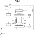
- FIG. 2 is a schematic diagram illustrating an exposure apparatus as an example of the lithography apparatus.
- An exposure apparatus 204 according to the present exemplary embodiment will be described as a step-and-scan type exposure apparatus (scanner) that executes exposure processing while synchronously driving a reticle stage and a wafer stage.
- the exposure apparatus 204 is not limited to a scanner, but may be a step-and-repeat type exposure apparatus (stepper) that executes exposure processing on a wafer while a wafer stage is in a stationary state.
- the exposure apparatus 204 includes a light source 7, an illumination optical system 8, a reticle stage 2, a projection optical system 3, a wafer stage 6, a wafer chuck 5, and a control unit 16.
- the exposure apparatus 204 further includes laser interferometers 9 and 10, a focus sensor 11, a wafer conveyance unit 12, a reticle conveyance unit 14, and an alignment scope 15.
- a direction parallel to the optical axis of the projection optical system 3 is defined as a Z-axis direction, and two directions orthogonal to each other in a plane perpendicular to the Z-axis direction are defined as an X-axis direction and a Y-axis direction respectively.
- a high-pressure mercury lamp, an argon-fluoride (ArF) excimer laser device, or a krypton-fluoride (KrF) excimer laser device may be used as the light source 7.
- the light source 7 does not always have to be arranged inside a chamber of the exposure apparatus 204, but may be arranged externally.
- Light emitted from the light source 7 illuminates a reticle 1 (i.e., an original plate or a mask) (not illustrated) via the illumination optical system 8.
- a pattern that to be transferred onto the wafer 4 (i.e., substrate) on which a photosensitive material is applied is drawn on a reticle 1, and the reticle 1 is mounted on the reticle stage 2.
- the reticle stage 2 suctions and holds the reticle 1 via a reticle chuck (not illustrated).
- the reticle stage 2 is configured to be movable by a linear motor (not illustrated).
- the projection optical system 3 projects an image of the pattern drawn on the reticle 1 onto the wafer 4 placed on the wafer chuck 5 (i.e., exposure processing).
- a projection magnification e.g., 1/4 magnifications
- An area where the image of the pattern is projected is called as a shot area.
- a plurality of shot areas is set on the wafer 4, and projection is sequentially and repeatedly executed on the shot areas.
- the wafer stage 6 is driven by a linear motor (not illustrated) and moved in the X-direction and the Y-direction.
- the wafer chuck 5 is mounted on the wafer stage 6 to hold the wafer 4.
- the wafer stage 6 fixes a position of the wafer chuck 5 in the Z-direction, the ⁇ -direction, the ⁇ X-direction, and the ⁇ Y-direction, where ⁇ is an angle of the wafer on the X-Y plane, ⁇ X is the angle of the wafer on the Y-Z plane, and ⁇ Y is the angle of the wafer on the X-Z plane.
- the wafer 4 held by the wafer chuck 5 is moved by a driving the wafer stage 6 and the wafer chuck 5.
- the laser interferometer 9 measures a position of the reticle stage 2 in the Y-direction and the orientation of the reticle stage 2.
- the laser interferometer 9 includes a laser interferometer (not illustrated) for measuring a position in the X-direction of the reticle stage 2 in a similar manner.
- the laser interferometer 10 measures a position of the wafer stage 6 in the Y-direction, on which the wafer 4 is mounted, and the orientation of the wafer stage 6.
- the laser interferometer 10 includes a laser interferometer (not illustrated) for measuring a position of the wafer stage 6 in the X-direction in a similar manner. Based on the positions measured by the laser interferometers 9 and 10, positions of the reticle stage 2 and the wafer stage 6 are controlled by a control unit 16 described below.
- the focus sensor 11 includes a light projection system 11a for projecting light (a plurality of beams) onto the wafer 4, a light receiving system 11b for receiving light reflected on the wafer 4, and a detection unit (not illustrated) for detecting light from the light receiving system 11b and outputting a detection signal to the control unit 16.
- the light projection system 11a and the light receiving system 11b are arranged so as to interpose a vicinity of a light emitting portion of the projection optical system 3 therebetween.
- the light projection system 11a obliquely emits light to the wafer 4, and the light receiving system 11b takes in the reflected light on the opposite side thereof.
- the below-described control unit 16 Based on the detection signal detected by the focus sensor 11, the below-described control unit 16 measures a position of the wafer 4 in the Z-direction and controls the movement of the wafer 4 moved by the wafer stage 6.
- the wafer conveyance unit 12 conveys the wafer 4.
- the wafer conveyance unit 12 conveys the wafer 4 to the wafer stage 6 from a wafer storage container (not illustrated) for storing the wafer 4. Further, the wafer conveyance unit 12 conveys the wafer 4 to the wafer storage container from the wafer stage 6.
- the reticle conveyance unit 14 conveys the reticle 1.
- the reticle conveyance unit 14 conveys the reticle 1 to the reticle stage 2 from a reticle storage container (not illustrated) for storing the reticle 1. Further, the reticle conveyance unit 14 conveys the reticle 1 to the reticle storage container from the reticle stage 2.
- the alignment scope 15 captures an image of a mark formed on the wafer 4 to acquire a digital image signal in order to execute positioning (alignment) of the wafer 4 held by the wafer chuck 5.
- the alignment scope 15 includes an image sensor (not illustrated) for outputting a contrast image signal corresponding to brightness (contrast) of reflection light from the wafer 4 (i.e., contrast), and an analog-to-digital (A/D) conversion unit (not illustrated) for converting the contrast image signal acquired from the image sensor into a digital image signal.
- the below-described control unit 16 detects the position of the mark formed on the wafer 4 by using the acquired digital image signal and executes positioning of the wafer 4 by controlling the wafer stage 6 based on the position of the detected mark.
- the control unit 16 controls the processing for exposing the wafer 4 to light by executing operation control and adjustment control of respective units of the exposure apparatus 204.
- the control unit 16 is an information processing apparatus configured of a combination of all or a part of a programmable logic device (PLD) such as a field programmable gate array (FPGA), an application specific integrated circuit (ASIC), and a computer on which a program is built-in.
- PLD programmable logic device
- FPGA field programmable gate array
- ASIC application specific integrated circuit
- the control unit 16 may be configured of a plurality of information processing apparatuses.
- the control unit 16 may be arranged integrally with another part of the exposure apparatus 204 in a common housing, or may be arranged separately from another part of the exposure apparatus 204 in a separate housing.
- control unit 16 executes control to execute the exposure processing (lithographic processing) of the wafer 4 by applying the below-described processing condition acquired from the storage device.
- a processing condition applied to the exposure processing may include a conveyance condition that specifies a speed or a path for conveying the wafer 4 to the wafer stage 6 by the wafer conveyance unit 12.
- a processing condition applied to the exposure processing may include a positioning condition that specifies an error allowable when the wafer 4 is positioned by the wafer stage 6.
- a processing condition applied to the exposure processing may include a measurement condition that specifies an irradiation period and an irradiation timing of light when measurement is executed by the focus sensor 11.
- a processing condition applied to the exposure processing may include an exposure condition that specifies an identifier of the reticle 1, a layout of a shot area on the wafer 4, and an illumination mode when the wafer 4 is exposed to light.
- a processing condition applied to the exposure processing may include a setup condition including information such as an environmental condition for specifying a temperature and an atmospheric pressure inside the exposure apparatus 204, a model of the exposure apparatus 204, and a version of software.
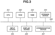
- Fig. 3 is a block diagram illustrating a hardware configuration of an information processing apparatus.
- Each of the hardware constituent elements of the information processing apparatus functions based on a program.
- a central processing unit (CPU) 301 is a processing device for executing calculation for executing control based on a program and controlling the respective constituent elements connected to a bus 308.
- a read only memory (ROM) 203 is a memory dedicated for reading out data, and a program and data are stored therein.
- a random access memory (RAM) 303 is a memory for reading and writing data, and is used for storing a program and data. The RAM 303 is used for temporarily storing data such as a calculation result acquired by the CPU 301.
- a storage device 304 is also used for storing a program and data.
- the storage device 304 is also used as an area for temporarily storing a program of an operating system (OS) for the information processing apparatus and data.
- OS operating system
- data input/output speed of the storage device 304 is slower than that of the RAM 303, a large volume of data can be stored in the storage device 304.
- the storage device 304 is a non-volatile storage device capable of storing data as persistent data, so that the stored data can be referred to for a long period of time.
- the storage device 304 is mainly configured of a magnetic storage device such as a hard disk drive (HDD), the storage device 304 may be a device that reads and writes data, on which an external media such as a compact disc (CD), a digital versatile disc (DVD), or a memory card is mounted.
- An input device 305 is a device for inputting text and data to the information processing apparatus, and a keyboard or a mouse corresponds thereto.
- a display device 306 is a device for displaying information or a processing result required for operating the information processing apparatus, and a cathode-ray tube monitor or a liquid crystal monitor corresponds thereto.
- a communication device 307 is used when the information processing apparatus connects to a network to execute data communication using a communication protocol such as a transmission control protocol/internet protocol (TCP/IP), and mutually communicates with another information processing apparatus.
- a communication protocol such as a transmission control protocol/internet protocol (TCP/IP)
- TCP/IP transmission control protocol/internet protocol
- the information processing apparatus may include a graphics processor unit (GPU) (not illustrated), so that calculation processing can be executed at high speed.
- GPU graphics processor unit
- the diagnosis apparatus 300 is an information processing apparatus including, for example, a configuration as illustrated in the example in Fig. 3 .
- the diagnosis apparatus 300 connects to a plurality of exposure apparatuses 204 via the communication device 307 to execute data communication.
- Fig. 4 is a block diagram illustrating a configuration of a CPU of the diagnosis apparatus 300.
- the CPU of the diagnosis apparatus 300 includes an acquisition unit 401, an accumulation unit 402, an abnormality judgement unit 403, a maintenance unit 404, and an output unit 405.
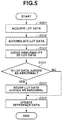
- Fig. 5 is a flowchart illustrating a method for judging an abnormality in the exposure apparatus 204.
- the acquisition unit 401 acquires lot data from the exposure apparatus 204. Further, the acquisition unit 401 acquires information for specifying the exposure apparatus 204 (e.g., an identification (ID) indicating the exposure apparatus 204) and information for specifying a processing condition applied when the lot data has been acquired (e.g., an ID indicating a processing condition) together with the lot data.
- ID identification
- a processing condition applied when the lot data has been acquired e.g., an ID indicating a processing condition
- Fig. 6 is a diagram illustrating an example of the lot data.
- the exposure apparatus 204 executes exposure processing of the wafer 4
- the exposure processing is executed in a unit of "lot" that includes a plurality of wafers 4 (e.g., 25 wafers 4). Further, the same processing condition is applied when the exposure processing is executed on the plurality of wafers 4 belonging to the same lot. Further, a layout of a plurality of shot areas (e.g., one hundred shot areas) is previously determined as exposure areas on the wafer 4, and the exposure apparatus 204 repeatedly executes exposure processing on the plurality of shot areas on the wafer 4. In the example in Fig. 6 , one lot includes 25 wafers 4, and one hundred shot areas are set with respect to each of the wafers 4. However, the number of wafers 4 or the shot areas are not limited thereto.
- the lot data is a collection of data collected when exposure processing is executed by applying the same processing condition to the plurality of wafers 4 belonging to the one lot described above.
- the lot data has a hierarchical structure, and pieces of collected data collected when exposure processing is executed on the plurality of shot areas of the wafer 4 are classified and stored for each wafer 4 or each shot area. Further, in the example in Fig. 6 , synchronization accuracy data and illuminance data are classified and stored for each shot area, and stage deviation data and alignment measurement data are classified and stored for each wafer 4.
- the synchronization accuracy data is data indicating an error in relative positions of the reticle stage 2 and the wafer stage 6, occurring in a period when the reticle stage 2 and the wafer stage 6 are synchronously driven in the Y-axis direction in order to expose a target shot area to light.
- the synchronization accuracy data is acquired by the control unit 16 based on the below-described stage deviation data of the reticle stage 2 and the wafer stage 6 collected during a period when the reticle stage 2 and the wafer stage 6 are driven synchronously. Because an increase in the synchronization accuracy data gives an influence on the overlay performance or the imaging performance, it is possible to judge an abnormality in the exposure apparatus 204 by monitoring the synchronization accuracy data.
- the illuminance data is a value representing intensity of light incident on the shot area during a period when the shot area is exposed to light.
- the illuminance data is acquired by the control unit 16 based on a measurement result acquired by a light amount sensor (not illustrated) for measuring light intensity arranged in the illumination optical system 8 during a period when the shot area is exposed to light.
- the stage deviation data is a value representing a deviation between a target position and a measurement position occurring when at least any one of the reticle stage 2 and the wafer stage 6 is controlled in an exposure period of the wafer 4.
- the stage deviation data is acquired by the control unit 16 based on the measurement results acquired by the laser interferometers 9 and 10.
- the alignment measurement data may include waveform data of a digital image signal acquired by capturing an image of a mark formed on a target wafer 4 or data that represents evaluation of the digital image signal (i.e., symmetric property of the waveform data or contrast of the digital image signal).
- the alignment measurement data is acquired by the control unit 16 based on the measurement result acquired by the alignment scope 15.
- the collected data is not limited to the synchronization accuracy data, the illuminance data, the stage deviation data, and the alignment measurement data.
- the collected data may be time-series data, or may include at least any one of a maximum value, a minimum value, an average value, a median value, and a standard deviation acquired from the time-series data.
- the collected data may include information indicating a principal component vector acquired through principal component analysis.
- the control unit 16 of the exposure apparatus 204 the lot data is collected from the respective units or devices of the exposure apparatus 204 and is output to the diagnosis apparatus 300 via the communication device 307.
- the control unit 16 may output a piece of lot data to the diagnosis apparatus 300 or may collectively output a plurality of pieces of lot data to the diagnosis apparatus 300.
- the control unit 16 may store the lot data in the storage device 304 and output the lot data stored in the storage device 304.
- the control unit 16 may output information for specifying the exposure apparatus 204 or information for specifying a processing condition applied thereto when the lot data is collected.
- the accumulation unit 402 accumulates the lot data acquired by the acquisition unit 401 in accumulated data (i.e., first information) and stores the lot data in the storage device 304 of the diagnosis apparatus 300. Further, the accumulation unit 402 acquires information for specifying the exposure apparatus 204 and the information for specifying a processing condition from the acquisition unit 401, and classifies and accumulates the lot data for each exposure apparatus 204 or each processing condition. In other words, the accumulation unit 402 accumulates the acquired lot data in data of the exposure apparatus which is the same as the exposure apparatus associated with the acquired lot data and of the processing condition which is the same as the processing condition associated with the acquired data.
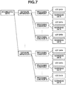
- Fig. 7 is a diagram illustrating an example of the accumulated data in which the lot data is accumulated.
- the accumulated data has a hierarchical structure, and lot data acquired from the plurality of exposure apparatuses 204 is classified and accumulated for each exposure apparatus or each processing condition.
- a plurality of pieces of lot data may be accumulated under the same processing condition.
- reference data (second information) including a statistical value of the plurality of pieces of lot data accumulated under the same processing condition is accumulated in the accumulated data.
- the example illustrated in Fig. 7 includes four exposure apparatuses 204 and ten processing conditions, the number of exposure apparatuses or processing conditions is not limited thereto.
- Fig. 8 is a diagram illustrating an example of the reference data accumulated in the accumulated data.
- the reference data includes a maximum value, a minimum value, an average value, a median value, a standard deviation, and an allowable range of collected data for each collected data included in lot data.
- the allowable range is used for judging an abnormality in the collected data, and an abnormality is judged if the collected data falls outside the allowable range.
- the reference data may include another statistical value such as a mode value, a variation coefficient, or a variance.
- data included in the reference data may be time-series data.
- data may be included in the reference data for each wafer or each shot area.
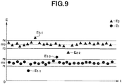
- Fig. 9 is a diagram illustrating an example of the synchronization accuracy data and the allowable range.
- pieces of synchronization accuracy data E 1 under the processing condition 1 are expressed by black dots
- pieces of synchronization accuracy data E 2 under the processing condition 2 are expressed by black triangles.
- values m 1 and m 2 respectively represent median values of the synchronization accuracy data E 1 and E 2 .
- a layout of the shot areas on the wafer 4 included in the exposure condition is different from each other, so that there arises a difference between the synchronization accuracy data E 1 and the synchronization accuracy data E 2 .
- the number of shot areas in the layout under the processing condition 1 is 100
- the number of shot areas in the layout under the processing condition 2 is 50.
- paths, speeds, and acceleration rates of the reticle stage 2 and the wafer stage 6 driven for executing the exposure processing are different because sizes of the shot areas are different from each other.
- a frequency of repeatedly accelerating and decelerating the reticle stage 2 or the wafer stage 6 is increased, so that an interval of repeatedly accelerating and decelerating the reticle stage 2 or the wafer stage 6 will be shorter. Accordingly, when the exposure processing is executed by applying the processing condition 1, a deviation in the reticle stage 2 and the wafer stage 6 is increased. As described above, because the synchronization accuracy data is obtained from the stage deviation data, the median value m 1 of the synchronization accuracy data E 1 tends to be greater than the median value m 2 of the synchronization accuracy data E 2 . Accordingly, as illustrated in Fig. 9 , the synchronization accuracy data is different from each other under the processing conditions 1 and 2.
- each of the median values m 1 and m 2 is a value included in the reference data of the same exposure apparatus under the same processing condition. Further, the median values m 1 and m 2 may be updated when a plurality of pieces of lot data accumulated in the accumulated data is updated.
- the synchronization accuracy data illustrated in Fig. 9 if the allowable range of the synchronization accuracy data is set as a range between a value r 1 or more and a value r 4 or less, the synchronization accuracy data E 1-2 and E 2-2 are judged as normal although the synchronization accuracy data E 1-1 and E 2-1 are judged as abnormal.
- the abnormality judgement unit 403 can judge the synchronization accuracy data E 1-2 and E 2-2 as abnormal by setting the allowable range of the synchronization accuracy data E 1 to a range between a value r 1 or more and a value r 2 or less and setting the allowable range of the synchronization accuracy data E 2 to a range between a value r 3 or more and a value r 4 or less.
- the abnormality judgement unit 403 can appropriately judge the abnormality by setting the allowable range for each processing condition.
- the values r 1 , r 2 , r 3 , and r 4 for setting the allowable range may be set in advance.
- the values r 1 , r 2 , r 3 , and r 4 for setting the allowable range may be set based on a difference with respect to the median value m 1 and m 2 .
- the allowable range is set by making the median value m 1 or m 2 as a reference, another statistical value such as a maximum value, a minimum value, or an average value may be used as a reference.
- the reference data is described as the reference data obtained under the same processing condition from the same exposure apparatus as the exposure apparatus from which the lot data is acquired, the exposure apparatus as a reference may be an exposure apparatus different from the exposure apparatus from which the lot data is acquired under the same processing condition.
- the synchronization accuracy data of the present exemplary embodiment has been described, an abnormality is judged for each collected data if a plurality of pieces of collected data is included in the lot data.
- step S504 if an abnormality is judged as a result of the judgement in step S503 (YES in step S504), the processing proceeds to step S505. If an abnormality is not judged (NO in step S504), the processing proceeds to step S506.
- step S505 the abnormality judgement unit 403 stores, in the storage device 304 of the diagnosis apparatus 30, the information for specifying the exposure apparatus 204 from which the lot data judged as abnormal is acquired.
- the abnormality judgement unit 403 stores related data such as a processing condition of the lot data judged as abnormal and the collected data (e.g., synchronization accuracy data) judged as abnormal in the storage device 304 of the diagnosis apparatus 300.
- step S506 the accumulation unit 402 updates the reference data based on the plurality of pieces of lot data accumulated already and newly-accumulated lot data. For example, if the data to be update is based on a statistical value, the accumulation unit 402 calculates the statistical value and updates the reference data based on the plurality of pieces of lot data accumulated already and the newly-accumulated lot data. Further, if there is a plurality of pieces of collected data for which abnormalities are to be judged, the processing in steps S501 to S506 is repeatedly executed by the number of pieces of collected data.
- the abnormality judgement unit 403 can judge abnormalities classified into gradual levels by setting a plurality of allowable ranges.
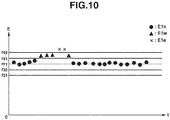
- Fig. 10 is a diagram illustrating examples of synchronization accuracy data and a plurality of allowable ranges.
- a plurality of allowable ranges are set by using values r 31 , r 32 , r 41 , and r 42 for setting the allowable ranges.
- the abnormality judgement unit 403 judges pieces of synchronization accuracy data E 1n (represented by black dots) falling within the allowable range between the value r 32 or more and the value r 41 or less as normal.
- the abnormality judgement unit 403 judges pieces of synchronization accuracy data E 1w (represented by black triangles) falling within the allowable range between the value r 31 or more and the value r 32 or less and the allowable range between the value r 41 or more and the value r 42 or less as slightly abnormal. Further, the abnormality judgement unit 403 judges pieces of synchronization accuracy data E 1e (represented by cross marks) falling within a range less than the value r 31 and a range greater than the value r 42 as considerably abnormal. With this configuration, the abnormality judgement unit 403 can judge the abnormalities classified into stepwise levels. For example, as with the case of the respective values for setting the allowable range illustrated in Fig.
- the values r 31 , r 32 , r 41 , and r 42 for setting the allowable ranges may be set in advance, or may be acquired through calculation.
- the values r 31 , r 32 , r 41 , and r 42 for setting the allowable ranges may be set based on a standard deviation calculated from data judged as normal from among pieces of the lot data of the accumulated data.
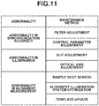
- the maintenance unit 404 determines a maintenance method for maintaining the exposure apparatus 204 from which the lot data judged as abnormal by the abnormality judgement unit 403 is acquired.
- a relationship between an abnormality judged in collected data and a maintenance method will be described.
- Fig. 11 is a table illustrating a relationship between a judged abnormality and a maintenance method. For example, with respect to an abnormality in synchronization accuracy judged in synchronization accuracy data, a filter adjustment or a control parameter adjustment may be selected as a maintenance method.
- the filter adjustment is a maintenance method for reducing the vibration arising in the wafer stage 6 or the reticle stage 2, and a filter that removes the vibration of a certain frequency component from an instruction value for controlling the wafer stage 6 or the reticle stage 2 is adjusted thereby.
- the control parameter adjustment is a maintenance method for adjusting a control parameter of the driving characteristic of the wafer stage 6 or the reticle stage 2 by the control unit 16.
- a slit adjustment or an optical axis adjustment may be selected as a maintenance method.
- the slit adjustment is a maintenance method for adjusting a slit included in the illumination optical system 8, so that exposure light is uniformly emitted when a shot area on the wafer 4 is to be exposed to light.
- the optical axis adjustment is a maintenance method for adjusting a telecentric state inside or outside the optical axis of the illumination optical system 8.
- sample shot search is a maintenance method in which the control unit 16 drives the wafer stage 6 and searches for another alignment mark at a specified alternative position on the wafer 4 to execute positioning by observing the wafer 4 through the alignment scope 15.
- the alignment illumination system optimization is a maintenance method for adjusting an alignment illumination system to increase the detection accuracy of the alignment mark.
- template update is a maintenance method for automatically updating a template so as to improve a correlation by the control unit 16 when the alignment mark is detected through template matching.
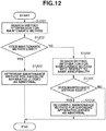
- Fig. 12 is a flowchart illustrating a method for determining a maintenance method.
- the maintenance unit 404 searches history information (third information) for a maintenance method corresponding to the collected data judged as abnormal.
- the history information will be described.
- Fig. 13 is a table illustrating an example of the history information.
- the history information may include information such as an abnormality type judged based on the collected data, date and time the collected data judged as abnormal is collected, an exposure apparatus from which the collected data judged as abnormal is collected, and a processing condition 1 or 2 applied when the collected data is collected.
- the history information may further include information such as a maintenance method executed for solving an abnormality and an execution result (i.e., "success" or "failure") indicating whether the executed maintenance method solves the abnormality.
- a maintenance method executed for solving an abnormality i.e., "success” or "failure"
- an execution result i.e., "success” or "failure”
- information about a maintenance method that has been executed for an abnormality occurred in an exposure apparatus in the past and an execution result of that maintenance method are recorded in the history information together with information about an exposure apparatus and a processing condition.
- the history information is acquired by the acquisition unit 401 of the diagnosis apparatus 300 and accumulated by the accumulation unit 402.
- the maintenance unit 404 searches history information for a maintenance method using such a search condition that data that describes "success" as an execution result from among the maintenance methods executed for the same abnormality occurring in the same exposure apparatus under the same processing condition.
- a search condition that data that describes "success” as an execution result from among the maintenance methods executed for the same abnormality occurring in the same exposure apparatus under the same processing condition.
- the maintenance unit 404 searches the history information for a maintenance method using such a search condition that data that describes "success" as an execution result of a maintenance method executed for the abnormality in synchronization accuracy occurring in the exposure apparatus 1 under the processing condition 1.
- Fig. 13 it is assumed that an abnormality in synchronization accuracy has occurred in an exposure apparatus 1 when exposure processing is executed by applying a processing condition 1.
- the maintenance unit 404 searches the history information for a maintenance method using such a search condition that data that describes "success" as an execution result of a maintenance method executed for the abnormality in synchronization accuracy occurring
- data listed in the first row is data matching the search condition, so that the filter adjustment is selected as the maintenance method.
- a maintenance method included in data having recent date and time or a maintenance method which results in success for a larger number of times in the plurality of data may be preferentially selected as a maintenance method matching the search condition.
- data including the same abnormality, the same exposure apparatus, and the same processing condition has been set as the search condition, data in which at least one of these items, i.e., the abnormality, the exposure apparatus, and the processing condition, is the same may be set as the search condition.
- step S1202 the maintenance unit 404 judges whether a maintenance method matching the search condition exists. If the maintenance unit 404 judges that a maintenance method matching the search condition exists (YES in step S1202), the processing proceeds to step S1203. In step S1203, the maintenance unit 404 determines the found maintenance method as the maintenance method of the exposure apparatus from which the collected data judged as abnormal is collected. Further, in step S1202, if the maintenance unit 404 judges that the maintenance method matching the search condition does not exist (NO in step S1202), the processing proceeds to step S1204.
- the maintenance unit 404 searches the information indicating a relationship between a predetermined abnormality and a maintenance method for a maintenance method corresponding to the judged abnormality. For example, if a relationship illustrated in Fig. 11 is determined in advance, filter adjustment and control parameter adjustment are found as the maintenance methods corresponding to the abnormality in synchronization accuracy. If a plurality of maintenance methods is found, a preset default maintenance method may be selected. For example, if control parameter adjustment is set as the default maintenance method, the control parameter adjustment is selected as a maintenance method. Further, a maintenance method stored in the history information and executed more frequently may be selected. For example, in the example in Fig.
- step S1205 filter adjustment as a maintenance method that is executed most frequently for the abnormality in synchronization accuracy is selected as a maintenance method.
- step S1205 the maintenance unit 404 judges whether a maintenance method matching the search condition exists. If the maintenance unit 404 judges that a maintenance method matching the search condition exists (YES in step S1205), the processing proceeds to step S1206. In step S1206, the maintenance unit 404 determines the found maintenance method as the maintenance method of the exposure apparatus from which the collected data judged as abnormal is collected. Further, in step S1205, if the maintenance unit 404 judges that the maintenance method matching the search condition does not exist (NO in step S1205), the processing is ended.
- the output unit 405 outputs an instruction (command) for executing the maintenance method determined by the maintenance unit 404 in step S1203 or S1206 to the exposure apparatus from which the collected data judged as abnormal is collected.
- the exposure apparatus that receives the instruction executes the maintenance method in response to the instruction.
- the output unit 405 may output an instruction for causing the exposure apparatus from which the collected data judged as abnormal is collected to output an error or a warning.
- the output unit 405 may output an instruction for causing the exposure apparatus from which the collected data judged as abnormal is collected to output a procedure for manually executing maintenance.
- the abnormality is judged based on the data accumulated for each processing condition applied to the lithography apparatus, so that an abnormality occurring in the lithography apparatus can be judged precisely. Further, a maintenance method is determined for the judged abnormality based on the history information including information about an executed maintenance method and its execution result, so that a maintenance method capable of solving the abnormality can be executed.
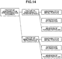
- Fig. 14 is a diagram illustrating a relationship between an abnormality and a factor of the abnormality.
- a factor of the abnormality in synchronization accuracy is classified into a factor of the abnormality in the wafer stage 6 and a factor of the abnormality in the reticle stage 2.
- An abnormality in an initial position, generation of vibration, and adhesion of foreign particles are considered as the factors of abnormalities in the wafer stage 6.
- the abnormality in the initial position refers to a state where an error of the initial position of the wafer stage 6 at the time of starting the exposure processing for each shot area falls outside the allowable range. Further, generation of vibration refers to a state where vibration is generated in the wafer stage 6. Further, adhesion of foreign particles refers to a state where foreign particles are adhered to the substrate or the wafer chuck 5. The same can apply to the factors of the abnormalities in the reticle stage 2.
- Fig. 15 is a flowchart illustrating a method for determining a maintenance method by using the factor analysis.
- the maintenance unit 404 acquires collected data judged as abnormal. At this time, it is assumed that the judged abnormality is the abnormality in synchronization accuracy, and the acquired collected data is the stage deviation data.
- Figs. 16A to 16D are graphs each illustrating an example of a waveform of a deviation in the wafer stage 6.
- a vertical axis represents a deviation and a horizontal axis represents time.
- Each of the graphs in Figs. 16A to 16D illustrates a waveform of a deviation during a period when exposure processing is sequentially executed on a plurality of shot areas on the wafer 4.
- Figs. 16A to 16D illustrates a waveform of a deviation during a period when exposure processing is sequentially executed on a plurality of shot areas on the wafer 4.
- FIG. 16A is a graph illustrating a state where the wafer stage 6 is controlled normally, so that the abnormality does not occur in the synchronization accuracy.
- Fig. 16B is a graph illustrating a state where the abnormality occurs in the synchronization accuracy because of the abnormality in the initial position.
- Fig. 16C is a graph illustrating a state where the abnormality occurs in the synchronization accuracy because of generation of vibration.
- a waveform of the deviation oscillates at a large amplitude over the entire period.
- Fig. 16D is a graph illustrating a state where foreign particles adheres to the wafer chuck 5, so that the abnormality occurs in the synchronization accuracy because of adhesion of the foreign particles.
- a waveform of the deviation in the wafer stage 6 has characteristics depending on the factors of the abnormalities in synchronization accuracy, so that the diagnosis apparatus 300 can estimate the factor of the abnormality in synchronization accuracy from the characteristics of the waveform of the deviation in the wafer stage 6.
- the maintenance unit 404 analyzes the collected data and estimates the factor of the occurring abnormality.
- a known technique such as factor estimation using a correlation coefficient or factor estimation using frequency analysis may be used as a method for estimating the factor of the abnormality.
- a method such as a decision tree, a random forest, a support vector machine, or a neural network may be employed by using the information about the collected data.
- the maintenance unit 404 searches the information (fourth information) about a relationship between the factor of the abnormality and the maintenance method for the maintenance method corresponding to the estimated factor.
- Fig. 17 is a table illustrating a relationship between a factor of an abnormality and a maintenance method.
- control parameter adjustment corresponds to the maintenance method.
- filter adjustment corresponds to the maintenance method.
- adhesion of foreign particles is estimated as a factor, chuck cleaning corresponds to the maintenance method.
- a relationship between a factor of an abnormality and a maintenance method in Fig. 17 is one example, and a relationship between a factor of an abnormality and a maintenance method is not limited to the example illustrated in Fig. 17 .
- step S1504 the maintenance unit 404 judges whether a maintenance method corresponding to the estimated factor exists. If the maintenance method exists (YES in step S1504), the processing proceeds to step S1505. If the maintenance method does not exist (NO in step S1504), the processing is ended. In step S1505, the maintenance unit 404 determines the found maintenance method as the maintenance method of the exposure apparatus from which the collected data judged as abnormal is collected.
- a maintenance method can be similarly determined for the reticle stage 2. Further, the determination method of the maintenance method described in the present exemplary embodiment may be executed in place of the determination method of the maintenance method described in the first exemplary embodiment, or the determination method of the maintenance method in the present exemplary embodiment may be executed in combination with the determination method of the maintenance method described in the first exemplary embodiment. In this case, a maintenance method may be determined by setting priorities to the maintenance methods determined through the two determination methods. Alternatively, a plurality of maintenance methods may be output to the exposure apparatus 204, so that a maintenance method may be selected by the exposure apparatus 204.
- a maintenance method is determined by estimating a factor of the abnormality in the lithography apparatus, so that a maintenance method capable of solving the abnormality can be determined.
- the lithography system according to the present exemplary embodiment includes a plurality of diagnosis apparatuses and a centralized management apparatus.
- Fig. 18 is a block diagram illustrating an example of the lithography system including a plurality of diagnosis apparatuses and a centralized management apparatus.
- a lithography system 101 according to the present exemplary embodiment includes lithography apparatuses 210 to 217, a first and a second diagnosis apparatuses 310 and 311 for judging abnormalities in the lithography apparatuses 210 to 217 to determine maintenance methods for maintaining the lithography apparatuses 210 to 217, and a centralized management apparatus 312.
- the lithography apparatuses 210 to 213 are connected to the first diagnosis apparatus 310, and the lithography apparatuses 214 to 217 are connected to the second diagnosis apparatus 311.
- the first diagnosis apparatus 310 and the second diagnosis apparatus 311 are connected to the centralized management apparatus 312.
- the number of lithography apparatuses is not limited to 8.
- the number of diagnosis apparatuses is not limited to 2.
- the first diagnosis apparatus 310, the second diagnosis apparatus 311, and the centralized management apparatus 312 are the information processing apparatuses described in the first exemplary embodiment.
- the centralized management apparatus 312 acquires lot data of the lithography apparatuses 210 to 217 via the first diagnosis apparatus 310 and the second diagnosis apparatus 311, and stores the lot data in the storage device 304 as accumulated data. Further, the centralized management apparatus 312 similarly acquires history information to store the history information in the storage device 304. Based on the accumulated data and the history information, the centralized management apparatus 312 acquires reference data, data for setting the allowable range of the collected data, data indicating a correspondence between an abnormality and a maintenance method, and data indicating a correspondence between a factor of an abnormality and a maintenance method.
- the centralized management apparatus 312 outputs the acquired information such as the reference data to the first diagnosis apparatus 310 and the second diagnosis apparatus 311. Based on the information such as the reference data acquired from the centralized management apparatus 312, the first diagnosis apparatus 310 and the second diagnosis apparatus 311 judge the abnormalities in the lithography apparatuses 210 to 217 and determine the maintenance methods. Each of the first and the second diagnosis apparatuses 310 and 311 can use the information such as the reference data acquired based on the lot data or the history information acquired from the other lithography apparatuses connected to another diagnosis apparatus.
- the centralized management apparatus 312 may periodically output the information such as the reference data to the first diagnosis apparatus 310 and the second diagnosis apparatus 311, or may output the information in response to a request from the first diagnosis apparatus 310 or the second diagnosis apparatus 311.
- a manufacturing method of an article according to the present exemplary embodiment is preferable for manufacturing an article, for example, a device such as a semiconductor device, a magnetic storage medium, and a liquid crystal display element.
- a manufacturing method includes a step of exposing a substrate on which a photosensitive agent is applied, to light (i.e., a pattern is formed on a substrate), and a step of developing the exposed substrate (i.e., the substrate is processed), by using an exposure apparatus. Further, such a manufacturing method includes a step of bringing an imprint material supplied on a substrate into contact with a mold, and forming a composition on which a shape of the mold is transferred, by using an imprint apparatus.
- such a manufacturing method may include other known steps, for example, oxidizing, film formation, vapor deposition, doping, planarization, etching, resist removing, die cutting, bonding, and packaging.
- the manufacturing method of an article according to the present exemplary embodiment is advantageous in at least one of performance, quality, productivity, and production cost of the article.
- An imprint apparatus which brings an imprint material supplied on a substrate into contact with a mold to form a composition on which a shape of the mold is transferred, may be also given as an example of the lithography apparatus.
- a drawing apparatus which executes drawing on a substrate with a charged-particle beam (e.g., an electron beam or an ion beam) via a charged-particle optical system to form a pattern on the substrate, may be given as an example of the lithography apparatus.
- a charged-particle beam e.g., an electron beam or an ion beam
- the lithography apparatus may also include a manufacturing apparatus such as an application apparatus for applying a photosensitive medium on a substrate of a substrate or a development apparatus for developing a substrate on which a pattern is transferred, which executes processing other than the processing executed by the above-described apparatus such as the imprint apparatus in the manufacture of an article such as a device.
- a manufacturing apparatus such as an application apparatus for applying a photosensitive medium on a substrate of a substrate or a development apparatus for developing a substrate on which a pattern is transferred, which executes processing other than the processing executed by the above-described apparatus such as the imprint apparatus in the manufacture of an article such as a device.
- first to the third exemplary embodiments can be implemented by combining the first to the third exemplary embodiments, in addition to being implemented independently.
- an information processing apparatus capable of precisely judging an abnormality occurring in a lithography apparatus, a judgement method, a program, a lithography apparatus, a lithography system, and a manufacturing method of an article.
- Embodiment(s) of the present invention can also be realized by a computer of a system or apparatus that reads out and executes computer executable instructions (e.g., one or more programs) recorded on a storage medium (which may also be referred to more fully as a 'non-transitory computer-readable storage medium') to perform the functions of one or more of the above-described embodiment(s) and/or that includes one or more circuits (e.g., application specific integrated circuit (ASIC)) for performing the functions of one or more of the above-described embodiment(s), and by a method performed by the computer of the system or apparatus by, for example, reading out and executing the computer executable instructions from the storage medium to perform the functions of one or more of the above-described embodiment(s) and/or controlling the one or more circuits to perform the functions of one or more of the above-described embodiment(s).
- computer executable instructions e.g., one or more programs
- a storage medium which may also be referred to more fully as
- the computer may comprise one or more processors (e.g., central processing unit (CPU), micro processing unit (MPU)) and may include a network of separate computers or separate processors to read out and execute the computer executable instructions.
- the computer executable instructions may be provided to the computer, for example, from a network or the storage medium.
- the storage medium may include, for example, one or more of a hard disk, a random-access memory (RAM), a read only memory (ROM), a storage of distributed computing systems, an optical disk (such as a compact disc (CD), digital versatile disc (DVD), or Blu-ray Disc (BD)TM), a flash memory device, a memory card, and the like.
Abstract
Description
- The present invention relates to an information processing apparatus, a method, a program, a lithography system, and a manufacturing method of an article.
- In the manufacture of an article such as a semiconductor device, micro-electro mechanical systems (MEMS), or a flat-panel display, because of progress in miniaturization of a pattern to be formed on a substrate, there is an increased demand for improvement in performance of a lithography apparatus, i.e., resolution, overlay accuracy, and productivity.
- In order to fulfill the demand for improvement in the performance of the lithography apparatus, it is necessary to solve the abnormality that may cause lowering of the performance of the lithography apparatus.
- Japanese Patent Application Laid-Open No.
2011-54804 - In the method described in Japanese Patent Application Laid-Open No.
2011-54804 - The present invention is directed to an information processing apparatus capable of precisely judging an abnormality occurring in a lithography apparatus, a judgement method, a program, a lithography system, and a manufacturing method of an article.
- According to a first aspect of the present invention, there is provided an information processing apparatus as specified in
claims 1 to 12. According to a second aspect of the present invention, there is provided a computer-implemented method of determining a maintenance method for a lithography apparatus as specified in claim 13. According to a third aspect of the present invention, there is provided a computer program as specified inclaim 14. According to a fourth aspect of the present invention, there is provided a lithography system as specified inclaim 15. According to a fifth aspect of the present invention, there is provided a manufacturing method as specified inclaim 16. - Further features of the present invention will become apparent from the following description of exemplary embodiments with reference to the attached drawings.
-
-
Fig. 1 is a block diagram illustrating a lithography system. -
Fig. 2 is a schematic diagram illustrating an exposure apparatus. -
Fig. 3 is a block diagram illustrating a hardware configuration of an information processing apparatus. -
Fig. 4 is a block diagram illustrating a configuration of a central processing unit (CPU) of a diagnosis apparatus. -
Fig. 5 is a flowchart illustrating a method of determining an abnormality in an exposure apparatus. -
Fig. 6 is a block diagram illustrating lot data. -
Fig. 7 is a block diagram illustrating accumulated data in which lot data is accumulated. -
Fig. 8 is a block diagram illustrating reference data accumulated in the accumulated data. -
Fig. 9 is a diagram illustrating synchronization accuracy data and an allowable range. -
Fig. 10 is a diagram illustrating synchronization accuracy data and a plurality of allowable ranges. -
Fig. 11 is a table illustrating an example of a relationship between a detected abnormality and a maintenance method. -
Fig. 12 is a flowchart illustrating a method of determining a maintenance method. -
Fig. 13 is a table illustrating history information. -
Fig. 14 is a block diagram illustrating a factor of an abnormality in synchronization accuracy. -
Fig. 15 is a flowchart illustrating a method of determining a maintenance method by employing factor analysis. -
Figs. 16A, 16B, 16C, and 16D are waveform charts illustrating waveforms of deviations arising in a wafer stage. -
Fig. 17 is a table illustrating a relationship between a factor of an abnormality and a maintenance method. -
Fig. 18 is a block diagram illustrating a lithography system configured of a plurality of diagnosis apparatuses and a centralized management apparatus. - Exemplary embodiments of the present invention will be described below in detail with reference to the appended drawings. In each of the drawings, the same reference number is applied to the same member, and duplicate description will be omitted.
- In a first exemplary embodiment, a lithography system including a plurality of lithography apparatuses and a diagnosis apparatus will be described.
Fig. 1 is a block diagram illustrating a lithography system. Alithography system 100 according to the present exemplary embodiment includeslithography apparatuses 200 to 203 each of which forms a pattern on a wafer (substrate) and adiagnosis apparatus 300 that judges an abnormality in a lithography apparatus to determine a maintenance method for executing maintenance of the lithography apparatus. The maintenance method for executing maintenance of the lithography apparatus is a method executed for solving an abnormality in the lithography apparatus. For example, in a case where an abnormality caused by an error regarding the position of the below-described wafer stage is judged, a maintenance method for reducing the vibration of the wafer stage may be executed in order to maintain the lithography apparatus. Further, the lithography apparatus may include an exposure apparatus which irradiates a reticle (i.e., a mask or an original plate) on which a pattern is formed with light, and projects the pattern on a shot area of a wafer by the light from the reticle. Further, for example, the lithography apparatus may include an imprint apparatus that brings an imprint material supplied on a wafer into contact with a mold (i.e., an original plate), and forms a composition on which a shape of the mold is transferred by applying curing energy to the imprint material. Furthermore, the lithography apparatus may include a drawing apparatus that draws a pattern on a substrate with a charged-particle beam (e.g., an electron beam or an ion beam) via a charged-particle optical system to form a pattern on the substrate. Further, for example, the lithography apparatus also may include a manufacturing apparatus such as an application apparatus for applying a photosensitive medium on a substrate or a development apparatus for developing a transferred pattern on a substrate, which executes processing other than the processing executed by the above-described apparatus such as the exposure apparatus in the manufacture of an article such as a device. Further, inFig. 1 , although thelithography apparatuses 200 to 203 are arranged, the number of lithography apparatuses is not limited to 4. - Next, an exposure apparatus will be described as an example of the
lithography apparatuses 200 to 203. The exposure apparatus exposes a wafer to light radiated from a reticle on which a pattern is formed.Fig. 2 is a schematic diagram illustrating an exposure apparatus as an example of the lithography apparatus. Anexposure apparatus 204 according to the present exemplary embodiment will be described as a step-and-scan type exposure apparatus (scanner) that executes exposure processing while synchronously driving a reticle stage and a wafer stage. However, theexposure apparatus 204 is not limited to a scanner, but may be a step-and-repeat type exposure apparatus (stepper) that executes exposure processing on a wafer while a wafer stage is in a stationary state. In the example inFig. 2 , theexposure apparatus 204 includes alight source 7, an illuminationoptical system 8, areticle stage 2, a projectionoptical system 3, awafer stage 6, awafer chuck 5, and acontrol unit 16. Theexposure apparatus 204 further includeslaser interferometers wafer conveyance unit 12, areticle conveyance unit 14, and analignment scope 15. In addition, inFig. 2 , a direction parallel to the optical axis of the projectionoptical system 3 is defined as a Z-axis direction, and two directions orthogonal to each other in a plane perpendicular to the Z-axis direction are defined as an X-axis direction and a Y-axis direction respectively. - For example, a high-pressure mercury lamp, an argon-fluoride (ArF) excimer laser device, or a krypton-fluoride (KrF) excimer laser device may be used as the
light source 7. Further, thelight source 7 does not always have to be arranged inside a chamber of theexposure apparatus 204, but may be arranged externally. Light emitted from thelight source 7 illuminates a reticle 1 (i.e., an original plate or a mask) (not illustrated) via the illuminationoptical system 8. A pattern that to be transferred onto the wafer 4 (i.e., substrate) on which a photosensitive material is applied is drawn on areticle 1, and thereticle 1 is mounted on thereticle stage 2. Thereticle stage 2 suctions and holds thereticle 1 via a reticle chuck (not illustrated). For example, thereticle stage 2 is configured to be movable by a linear motor (not illustrated). - The projection
optical system 3 projects an image of the pattern drawn on thereticle 1 onto thewafer 4 placed on the wafer chuck 5 (i.e., exposure processing). When the image of the pattern is projected on thewafer 4, the image that is inverted and reduced by a projection magnification (e.g., 1/4 magnifications) is projected on thewafer 4 via the projectionoptical system 3. An area where the image of the pattern is projected is called as a shot area. A plurality of shot areas is set on thewafer 4, and projection is sequentially and repeatedly executed on the shot areas. - The
wafer stage 6 is driven by a linear motor (not illustrated) and moved in the X-direction and the Y-direction. Thewafer chuck 5 is mounted on thewafer stage 6 to hold thewafer 4. Thewafer stage 6 fixes a position of thewafer chuck 5 in the Z-direction, the θ-direction, the ωX-direction, and the ωY-direction, where θ is an angle of the wafer on the X-Y plane, ωX is the angle of the wafer on the Y-Z plane, and ωY is the angle of the wafer on the X-Z plane. As described above, thewafer 4 held by thewafer chuck 5 is moved by a driving thewafer stage 6 and thewafer chuck 5. - The
laser interferometer 9 measures a position of thereticle stage 2 in the Y-direction and the orientation of thereticle stage 2. Thelaser interferometer 9 includes a laser interferometer (not illustrated) for measuring a position in the X-direction of thereticle stage 2 in a similar manner. Further, thelaser interferometer 10 measures a position of thewafer stage 6 in the Y-direction, on which thewafer 4 is mounted, and the orientation of thewafer stage 6. Further, thelaser interferometer 10 includes a laser interferometer (not illustrated) for measuring a position of thewafer stage 6 in the X-direction in a similar manner. Based on the positions measured by thelaser interferometers reticle stage 2 and thewafer stage 6 are controlled by acontrol unit 16 described below. - The focus sensor 11 includes a
light projection system 11a for projecting light (a plurality of beams) onto thewafer 4, alight receiving system 11b for receiving light reflected on thewafer 4, and a detection unit (not illustrated) for detecting light from thelight receiving system 11b and outputting a detection signal to thecontrol unit 16. Thelight projection system 11a and thelight receiving system 11b are arranged so as to interpose a vicinity of a light emitting portion of the projectionoptical system 3 therebetween. Thelight projection system 11a obliquely emits light to thewafer 4, and thelight receiving system 11b takes in the reflected light on the opposite side thereof. Based on the detection signal detected by the focus sensor 11, the below-describedcontrol unit 16 measures a position of thewafer 4 in the Z-direction and controls the movement of thewafer 4 moved by thewafer stage 6. - The
wafer conveyance unit 12 conveys thewafer 4. Thewafer conveyance unit 12 conveys thewafer 4 to thewafer stage 6 from a wafer storage container (not illustrated) for storing thewafer 4. Further, thewafer conveyance unit 12 conveys thewafer 4 to the wafer storage container from thewafer stage 6. - The
reticle conveyance unit 14 conveys thereticle 1. Thereticle conveyance unit 14 conveys thereticle 1 to thereticle stage 2 from a reticle storage container (not illustrated) for storing thereticle 1. Further, thereticle conveyance unit 14 conveys thereticle 1 to the reticle storage container from thereticle stage 2. - The
alignment scope 15 captures an image of a mark formed on thewafer 4 to acquire a digital image signal in order to execute positioning (alignment) of thewafer 4 held by thewafer chuck 5. Thealignment scope 15 includes an image sensor (not illustrated) for outputting a contrast image signal corresponding to brightness (contrast) of reflection light from the wafer 4 (i.e., contrast), and an analog-to-digital (A/D) conversion unit (not illustrated) for converting the contrast image signal acquired from the image sensor into a digital image signal. The below-describedcontrol unit 16 detects the position of the mark formed on thewafer 4 by using the acquired digital image signal and executes positioning of thewafer 4 by controlling thewafer stage 6 based on the position of the detected mark. - The
control unit 16 controls the processing for exposing thewafer 4 to light by executing operation control and adjustment control of respective units of theexposure apparatus 204. Thecontrol unit 16 is an information processing apparatus configured of a combination of all or a part of a programmable logic device (PLD) such as a field programmable gate array (FPGA), an application specific integrated circuit (ASIC), and a computer on which a program is built-in. Further, thecontrol unit 16 may be configured of a plurality of information processing apparatuses. Further, thecontrol unit 16 may be arranged integrally with another part of theexposure apparatus 204 in a common housing, or may be arranged separately from another part of theexposure apparatus 204 in a separate housing. Further, thecontrol unit 16 executes control to execute the exposure processing (lithographic processing) of thewafer 4 by applying the below-described processing condition acquired from the storage device. For example, a processing condition applied to the exposure processing may include a conveyance condition that specifies a speed or a path for conveying thewafer 4 to thewafer stage 6 by thewafer conveyance unit 12. Further, for example, a processing condition applied to the exposure processing may include a positioning condition that specifies an error allowable when thewafer 4 is positioned by thewafer stage 6. Furthermore, for example, a processing condition applied to the exposure processing may include a measurement condition that specifies an irradiation period and an irradiation timing of light when measurement is executed by the focus sensor 11. Further, for example, a processing condition applied to the exposure processing may include an exposure condition that specifies an identifier of thereticle 1, a layout of a shot area on thewafer 4, and an illumination mode when thewafer 4 is exposed to light. Further, for example, a processing condition applied to the exposure processing may include a setup condition including information such as an environmental condition for specifying a temperature and an atmospheric pressure inside theexposure apparatus 204, a model of theexposure apparatus 204, and a version of software. -
Fig. 3 is a block diagram illustrating a hardware configuration of an information processing apparatus. Each of the hardware constituent elements of the information processing apparatus functions based on a program. In the example inFig. 3 , a central processing unit (CPU) 301 is a processing device for executing calculation for executing control based on a program and controlling the respective constituent elements connected to abus 308. A read only memory (ROM) 203 is a memory dedicated for reading out data, and a program and data are stored therein. A random access memory (RAM) 303 is a memory for reading and writing data, and is used for storing a program and data. TheRAM 303 is used for temporarily storing data such as a calculation result acquired by theCPU 301. Astorage device 304 is also used for storing a program and data. Thestorage device 304 is also used as an area for temporarily storing a program of an operating system (OS) for the information processing apparatus and data. Although data input/output speed of thestorage device 304 is slower than that of theRAM 303, a large volume of data can be stored in thestorage device 304. It is desirable that thestorage device 304 is a non-volatile storage device capable of storing data as persistent data, so that the stored data can be referred to for a long period of time. Although thestorage device 304 is mainly configured of a magnetic storage device such as a hard disk drive (HDD), thestorage device 304 may be a device that reads and writes data, on which an external media such as a compact disc (CD), a digital versatile disc (DVD), or a memory card is mounted. Aninput device 305 is a device for inputting text and data to the information processing apparatus, and a keyboard or a mouse corresponds thereto. Adisplay device 306 is a device for displaying information or a processing result required for operating the information processing apparatus, and a cathode-ray tube monitor or a liquid crystal monitor corresponds thereto. Acommunication device 307 is used when the information processing apparatus connects to a network to execute data communication using a communication protocol such as a transmission control protocol/internet protocol (TCP/IP), and mutually communicates with another information processing apparatus. Further, the information processing apparatus may include a graphics processor unit (GPU) (not illustrated), so that calculation processing can be executed at high speed. - Next, a
diagnosis apparatus 300 will be described. Thediagnosis apparatus 300 is an information processing apparatus including, for example, a configuration as illustrated in the example inFig. 3 . Thediagnosis apparatus 300 connects to a plurality ofexposure apparatuses 204 via thecommunication device 307 to execute data communication.Fig. 4 is a block diagram illustrating a configuration of a CPU of thediagnosis apparatus 300. The CPU of thediagnosis apparatus 300 includes anacquisition unit 401, anaccumulation unit 402, an abnormality judgement unit 403, amaintenance unit 404, and anoutput unit 405. - Next, a method for judging an abnormality in the
exposure apparatus 204 by thediagnosis apparatus 300 will be described.Fig. 5 is a flowchart illustrating a method for judging an abnormality in theexposure apparatus 204. First, in step S501, theacquisition unit 401 acquires lot data from theexposure apparatus 204. Further, theacquisition unit 401 acquires information for specifying the exposure apparatus 204 (e.g., an identification (ID) indicating the exposure apparatus 204) and information for specifying a processing condition applied when the lot data has been acquired (e.g., an ID indicating a processing condition) together with the lot data. - Here, the lot data will be described.
Fig. 6 is a diagram illustrating an example of the lot data. When theexposure apparatus 204 executes exposure processing of thewafer 4, the exposure processing is executed in a unit of "lot" that includes a plurality of wafers 4 (e.g., 25 wafers 4). Further, the same processing condition is applied when the exposure processing is executed on the plurality ofwafers 4 belonging to the same lot. Further, a layout of a plurality of shot areas (e.g., one hundred shot areas) is previously determined as exposure areas on thewafer 4, and theexposure apparatus 204 repeatedly executes exposure processing on the plurality of shot areas on thewafer 4. In the example inFig. 6 , one lot includes 25wafers 4, and one hundred shot areas are set with respect to each of thewafers 4. However, the number ofwafers 4 or the shot areas are not limited thereto. - The lot data is a collection of data collected when exposure processing is executed by applying the same processing condition to the plurality of
wafers 4 belonging to the one lot described above. The lot data has a hierarchical structure, and pieces of collected data collected when exposure processing is executed on the plurality of shot areas of thewafer 4 are classified and stored for eachwafer 4 or each shot area. Further, in the example inFig. 6 , synchronization accuracy data and illuminance data are classified and stored for each shot area, and stage deviation data and alignment measurement data are classified and stored for eachwafer 4. Here, for example, the synchronization accuracy data is data indicating an error in relative positions of thereticle stage 2 and thewafer stage 6, occurring in a period when thereticle stage 2 and thewafer stage 6 are synchronously driven in the Y-axis direction in order to expose a target shot area to light. Further, the synchronization accuracy data is acquired by thecontrol unit 16 based on the below-described stage deviation data of thereticle stage 2 and thewafer stage 6 collected during a period when thereticle stage 2 and thewafer stage 6 are driven synchronously. Because an increase in the synchronization accuracy data gives an influence on the overlay performance or the imaging performance, it is possible to judge an abnormality in theexposure apparatus 204 by monitoring the synchronization accuracy data. Further, the illuminance data is a value representing intensity of light incident on the shot area during a period when the shot area is exposed to light. For example, the illuminance data is acquired by thecontrol unit 16 based on a measurement result acquired by a light amount sensor (not illustrated) for measuring light intensity arranged in the illuminationoptical system 8 during a period when the shot area is exposed to light. Further, the stage deviation data is a value representing a deviation between a target position and a measurement position occurring when at least any one of thereticle stage 2 and thewafer stage 6 is controlled in an exposure period of thewafer 4. The stage deviation data is acquired by thecontrol unit 16 based on the measurement results acquired by thelaser interferometers target wafer 4 or data that represents evaluation of the digital image signal (i.e., symmetric property of the waveform data or contrast of the digital image signal). The alignment measurement data is acquired by thecontrol unit 16 based on the measurement result acquired by thealignment scope 15. Further, the collected data is not limited to the synchronization accuracy data, the illuminance data, the stage deviation data, and the alignment measurement data. For example, the collected data may be time-series data, or may include at least any one of a maximum value, a minimum value, an average value, a median value, and a standard deviation acquired from the time-series data. Further, the collected data may include information indicating a principal component vector acquired through principal component analysis. Further, by thecontrol unit 16 of theexposure apparatus 204, the lot data is collected from the respective units or devices of theexposure apparatus 204 and is output to thediagnosis apparatus 300 via thecommunication device 307. Here, thecontrol unit 16 may output a piece of lot data to thediagnosis apparatus 300 or may collectively output a plurality of pieces of lot data to thediagnosis apparatus 300. Further, thecontrol unit 16 may store the lot data in thestorage device 304 and output the lot data stored in thestorage device 304. Furthermore, together with the lot data, thecontrol unit 16 may output information for specifying theexposure apparatus 204 or information for specifying a processing condition applied thereto when the lot data is collected. - Referring back to
Fig. 5 , in step S502, theaccumulation unit 402 accumulates the lot data acquired by theacquisition unit 401 in accumulated data (i.e., first information) and stores the lot data in thestorage device 304 of thediagnosis apparatus 300. Further, theaccumulation unit 402 acquires information for specifying theexposure apparatus 204 and the information for specifying a processing condition from theacquisition unit 401, and classifies and accumulates the lot data for eachexposure apparatus 204 or each processing condition. In other words, theaccumulation unit 402 accumulates the acquired lot data in data of the exposure apparatus which is the same as the exposure apparatus associated with the acquired lot data and of the processing condition which is the same as the processing condition associated with the acquired data. - Here, accumulated data in which the lot data acquired from the plurality of
exposure apparatuses 204 is accumulated will be described.Fig. 7 is a diagram illustrating an example of the accumulated data in which the lot data is accumulated. The accumulated data has a hierarchical structure, and lot data acquired from the plurality ofexposure apparatuses 204 is classified and accumulated for each exposure apparatus or each processing condition. In a case where exposure processing is executed on a plurality of lots by oneexposure apparatus 204 under the same processing condition, a plurality of pieces of lot data may be accumulated under the same processing condition. Further, reference data (second information) including a statistical value of the plurality of pieces of lot data accumulated under the same processing condition is accumulated in the accumulated data. In addition, although the example illustrated inFig. 7 includes fourexposure apparatuses 204 and ten processing conditions, the number of exposure apparatuses or processing conditions is not limited thereto. - One example of the reference data will be described.
Fig. 8 is a diagram illustrating an example of the reference data accumulated in the accumulated data. The reference data includes a maximum value, a minimum value, an average value, a median value, a standard deviation, and an allowable range of collected data for each collected data included in lot data. In the present exemplary embodiment, the allowable range is used for judging an abnormality in the collected data, and an abnormality is judged if the collected data falls outside the allowable range. Further, the reference data may include another statistical value such as a mode value, a variation coefficient, or a variance. Furthermore, data included in the reference data may be time-series data. In addition, as with the case of lot data, data may be included in the reference data for each wafer or each shot area. - Referring back to
Fig. 5 , in step S503, the abnormality judgement unit 403 judges an abnormality by using the lot data accumulated by theaccumulation unit 402 and the reference data. An abnormality judgement method using synchronization accuracy data from among the plurality of pieces of data included in the lot data will be described as an example.Fig. 9 is a diagram illustrating an example of the synchronization accuracy data and the allowable range. InFig. 9 , pieces of synchronization accuracy data E1 under theprocessing condition 1 are expressed by black dots, and pieces of synchronization accuracy data E2 under theprocessing condition 2 are expressed by black triangles. Further, values m1 and m2 respectively represent median values of the synchronization accuracy data E1 and E2. For example, under theprocessing conditions wafer 4 included in the exposure condition is different from each other, so that there arises a difference between the synchronization accuracy data E1 and the synchronization accuracy data E2. For example, it is assumed that the number of shot areas in the layout under theprocessing condition 1 is 100, and the number of shot areas in the layout under theprocessing condition 2 is 50. In this case, paths, speeds, and acceleration rates of thereticle stage 2 and thewafer stage 6 driven for executing the exposure processing are different because sizes of the shot areas are different from each other. When the exposure processing is executed by applying theprocessing condition 1, a frequency of repeatedly accelerating and decelerating thereticle stage 2 or thewafer stage 6 is increased, so that an interval of repeatedly accelerating and decelerating thereticle stage 2 or thewafer stage 6 will be shorter. Accordingly, when the exposure processing is executed by applying theprocessing condition 1, a deviation in thereticle stage 2 and thewafer stage 6 is increased. As described above, because the synchronization accuracy data is obtained from the stage deviation data, the median value m1 of the synchronization accuracy data E1 tends to be greater than the median value m2 of the synchronization accuracy data E2. Accordingly, as illustrated inFig. 9 , the synchronization accuracy data is different from each other under theprocessing conditions Fig. 9 , if the allowable range of the synchronization accuracy data is set as a range between a value r1 or more and a value r4 or less, the synchronization accuracy data E1-2 and E2-2 are judged as normal although the synchronization accuracy data E1-1 and E2-1 are judged as abnormal. However, when observing the synchronization accuracy data for each processing condition, the synchronization accuracy data E1-2 and E2-2 respectively deviate largely from the median values m1 and m2, so that the synchronization accuracy data E1-2 and E2-2 should be judged as the abnormal synchronization accuracy data. Thus, the abnormality judgement unit 403 can judge the synchronization accuracy data E1-2 and E2-2 as abnormal by setting the allowable range of the synchronization accuracy data E1 to a range between a value r1 or more and a value r2 or less and setting the allowable range of the synchronization accuracy data E2 to a range between a value r3 or more and a value r4 or less. In other words, the abnormality judgement unit 403 can appropriately judge the abnormality by setting the allowable range for each processing condition. Further, the values r1, r2, r3, and r4 for setting the allowable range may be set in advance. Further, the values r1, r2, r3, and r4 for setting the allowable range may be set based on a difference with respect to the median value m1 and m2. More specifically, the respective values r1, r2, r3, and r4 may be set as r1 = m1 - a, r2 = m1 + b, r3 = m2 - c, and r4 = m2 + d (values a, b, c, and d are predetermined positive values). Further, the values r1, r2, r3, and r4 for setting the allowable range may be set based on a ratio with respect to the median value m1 and m2. More specifically, the respective values r1, r2, r3, and r4 may be set as r1 = em1, r2 = fm1, r3 = gm2, and r4 = hm2 (values e, f, g, and h are predetermined positive values which respectively satisfy the conditions of e > 1, 1 < f < 0, g > 1, and 1 < h < 0). Further, the values r1, r2, r3, and r4 for setting the allowable range may be acquired through calculation based on the accumulated data. For example, the values r1, r2, r3, and r4 for setting the allowable range may be set based on a standard deviation calculated from data judged as normal from among the lot data of the accumulated data. More specifically, the respective values r1, r2, r3, and r4 may be set as r1 = m1 - σ1, r2 = m1 + σ1, r3 = m2 - σ2, and r4 = m2 + σ2 (values σ1 and σ2 are standard deviations). Further, although the allowable range is set by making the median value m1 or m2 as a reference, another statistical value such as a maximum value, a minimum value, or an average value may be used as a reference. Further, although the reference data is described as the reference data obtained under the same processing condition from the same exposure apparatus as the exposure apparatus from which the lot data is acquired, the exposure apparatus as a reference may be an exposure apparatus different from the exposure apparatus from which the lot data is acquired under the same processing condition. Further, although the synchronization accuracy data of the present exemplary embodiment has been described, an abnormality is judged for each collected data if a plurality of pieces of collected data is included in the lot data. - Referring back to
Fig. 5 , in step S504, if an abnormality is judged as a result of the judgement in step S503 (YES in step S504), the processing proceeds to step S505. If an abnormality is not judged (NO in step S504), the processing proceeds to step S506. In step S505, the abnormality judgement unit 403 stores, in thestorage device 304 of the diagnosis apparatus 30, the information for specifying theexposure apparatus 204 from which the lot data judged as abnormal is acquired. Further, together with the information for specifying theexposure apparatus 204, the abnormality judgement unit 403 stores related data such as a processing condition of the lot data judged as abnormal and the collected data (e.g., synchronization accuracy data) judged as abnormal in thestorage device 304 of thediagnosis apparatus 300. - In step S506, the
accumulation unit 402 updates the reference data based on the plurality of pieces of lot data accumulated already and newly-accumulated lot data. For example, if the data to be update is based on a statistical value, theaccumulation unit 402 calculates the statistical value and updates the reference data based on the plurality of pieces of lot data accumulated already and the newly-accumulated lot data. Further, if there is a plurality of pieces of collected data for which abnormalities are to be judged, the processing in steps S501 to S506 is repeatedly executed by the number of pieces of collected data. - Further, in step S503, the abnormality judgement unit 403 can judge abnormalities classified into gradual levels by setting a plurality of allowable ranges.
Fig. 10 is a diagram illustrating examples of synchronization accuracy data and a plurality of allowable ranges. InFig. 10 , with respect to the synchronization accuracy data E1 under theprocessing condition 1, a plurality of allowable ranges are set by using values r31, r32, r41, and r42 for setting the allowable ranges. The abnormality judgement unit 403 judges pieces of synchronization accuracy data E1n (represented by black dots) falling within the allowable range between the value r32 or more and the value r41 or less as normal. Further, the abnormality judgement unit 403 judges pieces of synchronization accuracy data E1w (represented by black triangles) falling within the allowable range between the value r31 or more and the value r32 or less and the allowable range between the value r41 or more and the value r42 or less as slightly abnormal. Further, the abnormality judgement unit 403 judges pieces of synchronization accuracy data E1e (represented by cross marks) falling within a range less than the value r31 and a range greater than the value r42 as considerably abnormal. With this configuration, the abnormality judgement unit 403 can judge the abnormalities classified into stepwise levels. For example, as with the case of the respective values for setting the allowable range illustrated inFig. 9 , the values r31, r32, r41, and r42 for setting the allowable ranges may be set in advance, or may be acquired through calculation. For example, the values r31, r32, r41, and r42 for setting the allowable ranges may be set based on a standard deviation calculated from data judged as normal from among pieces of the lot data of the accumulated data. For example, the respective values r31, r32, r41, and r42 may be set as r31 = m1 - iσ1, r32 = m1 - jσ1, r41 = m1 + jσ1, and r42 = m1 + iσ1, where the value σ1 is a standard deviation, and the values i and j are positive values which satisfy the condition i > j. - Next, a method of determining a maintenance method for maintaining the
exposure apparatus 204 from which the lot data judged as abnormal by thediagnosis apparatus 300 is acquired will be described. Themaintenance unit 404 determines a maintenance method for maintaining theexposure apparatus 204 from which the lot data judged as abnormal by the abnormality judgement unit 403 is acquired. Here, a relationship between an abnormality judged in collected data and a maintenance method will be described.Fig. 11 is a table illustrating a relationship between a judged abnormality and a maintenance method. For example, with respect to an abnormality in synchronization accuracy judged in synchronization accuracy data, a filter adjustment or a control parameter adjustment may be selected as a maintenance method. The filter adjustment is a maintenance method for reducing the vibration arising in thewafer stage 6 or thereticle stage 2, and a filter that removes the vibration of a certain frequency component from an instruction value for controlling thewafer stage 6 or thereticle stage 2 is adjusted thereby. The control parameter adjustment is a maintenance method for adjusting a control parameter of the driving characteristic of thewafer stage 6 or thereticle stage 2 by thecontrol unit 16. - Further, with respect to an abnormality in illuminance judged in illuminance data, a slit adjustment or an optical axis adjustment may be selected as a maintenance method. The slit adjustment is a maintenance method for adjusting a slit included in the illumination
optical system 8, so that exposure light is uniformly emitted when a shot area on thewafer 4 is to be exposed to light. The optical axis adjustment is a maintenance method for adjusting a telecentric state inside or outside the optical axis of the illuminationoptical system 8. - Further, for an abnormality in alignment measurement judged in the alignment measurement data, sample shot search, alignment illumination system optimization, or template update may be selected as a maintenance method. The sample shot search is a maintenance method in which the
control unit 16 drives thewafer stage 6 and searches for another alignment mark at a specified alternative position on thewafer 4 to execute positioning by observing thewafer 4 through thealignment scope 15. Further, the alignment illumination system optimization is a maintenance method for adjusting an alignment illumination system to increase the detection accuracy of the alignment mark. The template update is a maintenance method for automatically updating a template so as to improve a correlation by thecontrol unit 16 when the alignment mark is detected through template matching. -
Fig. 12 is a flowchart illustrating a method for determining a maintenance method. In step S1201, themaintenance unit 404 searches history information (third information) for a maintenance method corresponding to the collected data judged as abnormal. Here, the history information will be described.Fig. 13 is a table illustrating an example of the history information. The history information may include information such as an abnormality type judged based on the collected data, date and time the collected data judged as abnormal is collected, an exposure apparatus from which the collected data judged as abnormal is collected, and aprocessing condition acquisition unit 401 of thediagnosis apparatus 300 and accumulated by theaccumulation unit 402. - Referring back to
Fig. 12 , in step S1201, themaintenance unit 404 searches history information for a maintenance method using such a search condition that data that describes "success" as an execution result from among the maintenance methods executed for the same abnormality occurring in the same exposure apparatus under the same processing condition. For example, as illustrated inFig. 13 , it is assumed that an abnormality in synchronization accuracy has occurred in anexposure apparatus 1 when exposure processing is executed by applying aprocessing condition 1. In this case, themaintenance unit 404 searches the history information for a maintenance method using such a search condition that data that describes "success" as an execution result of a maintenance method executed for the abnormality in synchronization accuracy occurring in theexposure apparatus 1 under theprocessing condition 1. In the example illustrated inFig. 13 , data listed in the first row is data matching the search condition, so that the filter adjustment is selected as the maintenance method. Here, if there are pieces of data matching the search condition, a maintenance method included in data having recent date and time or a maintenance method which results in success for a larger number of times in the plurality of data may be preferentially selected as a maintenance method matching the search condition. Further, at this time, although data including the same abnormality, the same exposure apparatus, and the same processing condition has been set as the search condition, data in which at least one of these items, i.e., the abnormality, the exposure apparatus, and the processing condition, is the same may be set as the search condition. - In step S1202, the
maintenance unit 404 judges whether a maintenance method matching the search condition exists. If themaintenance unit 404 judges that a maintenance method matching the search condition exists (YES in step S1202), the processing proceeds to step S1203. In step S1203, themaintenance unit 404 determines the found maintenance method as the maintenance method of the exposure apparatus from which the collected data judged as abnormal is collected. Further, in step S1202, if themaintenance unit 404 judges that the maintenance method matching the search condition does not exist (NO in step S1202), the processing proceeds to step S1204. - In step S1204, the
maintenance unit 404 searches the information indicating a relationship between a predetermined abnormality and a maintenance method for a maintenance method corresponding to the judged abnormality. For example, if a relationship illustrated inFig. 11 is determined in advance, filter adjustment and control parameter adjustment are found as the maintenance methods corresponding to the abnormality in synchronization accuracy. If a plurality of maintenance methods is found, a preset default maintenance method may be selected. For example, if control parameter adjustment is set as the default maintenance method, the control parameter adjustment is selected as a maintenance method. Further, a maintenance method stored in the history information and executed more frequently may be selected. For example, in the example inFig. 12 , filter adjustment as a maintenance method that is executed most frequently for the abnormality in synchronization accuracy is selected as a maintenance method. In step S1205, themaintenance unit 404 judges whether a maintenance method matching the search condition exists. If themaintenance unit 404 judges that a maintenance method matching the search condition exists (YES in step S1205), the processing proceeds to step S1206. In step S1206, themaintenance unit 404 determines the found maintenance method as the maintenance method of the exposure apparatus from which the collected data judged as abnormal is collected. Further, in step S1205, if themaintenance unit 404 judges that the maintenance method matching the search condition does not exist (NO in step S1205), the processing is ended. - The
output unit 405 outputs an instruction (command) for executing the maintenance method determined by themaintenance unit 404 in step S1203 or S1206 to the exposure apparatus from which the collected data judged as abnormal is collected. The exposure apparatus that receives the instruction executes the maintenance method in response to the instruction. Further, in step S1205, if themaintenance unit 404 judges that the maintenance method does not exist (NO in step S1205), theoutput unit 405 may output an instruction for causing the exposure apparatus from which the collected data judged as abnormal is collected to output an error or a warning. Further, if themaintenance unit 404 judges that the maintenance method does not exist in step S1205, theoutput unit 405 may output an instruction for causing the exposure apparatus from which the collected data judged as abnormal is collected to output a procedure for manually executing maintenance. - As described above, in the present exemplary embodiment, the abnormality is judged based on the data accumulated for each processing condition applied to the lithography apparatus, so that an abnormality occurring in the lithography apparatus can be judged precisely. Further, a maintenance method is determined for the judged abnormality based on the history information including information about an executed maintenance method and its execution result, so that a maintenance method capable of solving the abnormality can be executed.
- In a second exemplary embodiment, an example of processing for determining a maintenance method by using factor analysis of an abnormality will be described. In addition, a configuration that is not described below may be similar to that of the first exemplary embodiment.
- Factor analysis of the abnormality judged by the abnormality judgement unit 403 will be described. In the present exemplary embodiment, an abnormality in synchronization accuracy will be described as an example of a detected abnormality.
Fig. 14 is a diagram illustrating a relationship between an abnormality and a factor of the abnormality. First, a factor of the abnormality in synchronization accuracy is classified into a factor of the abnormality in thewafer stage 6 and a factor of the abnormality in thereticle stage 2. An abnormality in an initial position, generation of vibration, and adhesion of foreign particles are considered as the factors of abnormalities in thewafer stage 6. The abnormality in the initial position refers to a state where an error of the initial position of thewafer stage 6 at the time of starting the exposure processing for each shot area falls outside the allowable range. Further, generation of vibration refers to a state where vibration is generated in thewafer stage 6. Further, adhesion of foreign particles refers to a state where foreign particles are adhered to the substrate or thewafer chuck 5. The same can apply to the factors of the abnormalities in thereticle stage 2. - Subsequently, a maintenance method for executing maintenance with respect to the factors specified by the factor analysis will be described.
Fig. 15 is a flowchart illustrating a method for determining a maintenance method by using the factor analysis. In step S1501, themaintenance unit 404 acquires collected data judged as abnormal. At this time, it is assumed that the judged abnormality is the abnormality in synchronization accuracy, and the acquired collected data is the stage deviation data. - Now, the stage deviation data will be described in a case where the
exposure apparatus 204 is a scanner.Figs. 16A to 16D are graphs each illustrating an example of a waveform of a deviation in thewafer stage 6. In each of the graphs inFigs. 16A to 16D , a vertical axis represents a deviation and a horizontal axis represents time. Each of the graphs inFigs. 16A to 16D illustrates a waveform of a deviation during a period when exposure processing is sequentially executed on a plurality of shot areas on thewafer 4. In each ofFigs. 16A to 16D , sections defined by dotted lines represent a period A in which the exposure processing is executed on a shot area and a period B in which the exposure processing is not executed. Because scanning-exposure processing is executed in the period A, thewafer stage 6 is driven and moved at a uniform speed. Further, in the period B, in order to move an exposure area to the next shot area, thewafer stage 6 is driven and moved at an accelerated speed.Fig. 16A is a graph illustrating a state where thewafer stage 6 is controlled normally, so that the abnormality does not occur in the synchronization accuracy.Fig. 16B is a graph illustrating a state where the abnormality occurs in the synchronization accuracy because of the abnormality in the initial position. When a factor of the abnormality is an abnormality in the initial position, a large deviation occurs at the beginning of the period A.Fig. 16C is a graph illustrating a state where the abnormality occurs in the synchronization accuracy because of generation of vibration. When a factor of the abnormality is generation of vibration, a waveform of the deviation oscillates at a large amplitude over the entire period. Further,Fig. 16D is a graph illustrating a state where foreign particles adheres to thewafer chuck 5, so that the abnormality occurs in the synchronization accuracy because of adhesion of the foreign particles. When a factor of the abnormality is a substrate, a considerable change occurs in a waveform of the deviation irregularly. As described above, a waveform of the deviation in thewafer stage 6 has characteristics depending on the factors of the abnormalities in synchronization accuracy, so that thediagnosis apparatus 300 can estimate the factor of the abnormality in synchronization accuracy from the characteristics of the waveform of the deviation in thewafer stage 6. - Referring back to
Fig. 15 , in step S1502, themaintenance unit 404 analyzes the collected data and estimates the factor of the occurring abnormality. A known technique such as factor estimation using a correlation coefficient or factor estimation using frequency analysis may be used as a method for estimating the factor of the abnormality. Furthermore, a method such as a decision tree, a random forest, a support vector machine, or a neural network may be employed by using the information about the collected data. In step S1503, themaintenance unit 404 searches the information (fourth information) about a relationship between the factor of the abnormality and the maintenance method for the maintenance method corresponding to the estimated factor. - Next, a relationship between a factor of an abnormality and a maintenance method will be described.
Fig. 17 is a table illustrating a relationship between a factor of an abnormality and a maintenance method. In step S1502, in a case where an abnormality in the initial position is estimated as a factor, control parameter adjustment corresponds to the maintenance method. Further, in a case where generation of vibration is estimated as a factor, filter adjustment corresponds to the maintenance method. Furthermore, in a case where adhesion of foreign particles is estimated as a factor, chuck cleaning corresponds to the maintenance method. A relationship between a factor of an abnormality and a maintenance method inFig. 17 is one example, and a relationship between a factor of an abnormality and a maintenance method is not limited to the example illustrated inFig. 17 . - Referring back to
Fig. 15 , in step S1504, themaintenance unit 404 judges whether a maintenance method corresponding to the estimated factor exists. If the maintenance method exists (YES in step S1504), the processing proceeds to step S1505. If the maintenance method does not exist (NO in step S1504), the processing is ended. In step S1505, themaintenance unit 404 determines the found maintenance method as the maintenance method of the exposure apparatus from which the collected data judged as abnormal is collected. - Although the
wafer stage 6 is described according to the present exemplary embodiment, a maintenance method can be similarly determined for thereticle stage 2. Further, the determination method of the maintenance method described in the present exemplary embodiment may be executed in place of the determination method of the maintenance method described in the first exemplary embodiment, or the determination method of the maintenance method in the present exemplary embodiment may be executed in combination with the determination method of the maintenance method described in the first exemplary embodiment. In this case, a maintenance method may be determined by setting priorities to the maintenance methods determined through the two determination methods. Alternatively, a plurality of maintenance methods may be output to theexposure apparatus 204, so that a maintenance method may be selected by theexposure apparatus 204. - As described above, a maintenance method is determined by estimating a factor of the abnormality in the lithography apparatus, so that a maintenance method capable of solving the abnormality can be determined.
- Next, a lithography system according to a third exemplary embodiment will be described. In addition, a configuration not described below is similar to that of the first or the second exemplary embodiment.
- The lithography system according to the present exemplary embodiment includes a plurality of diagnosis apparatuses and a centralized management apparatus.
Fig. 18 is a block diagram illustrating an example of the lithography system including a plurality of diagnosis apparatuses and a centralized management apparatus. Alithography system 101 according to the present exemplary embodiment includeslithography apparatuses 210 to 217, a first and asecond diagnosis apparatuses lithography apparatuses 210 to 217 to determine maintenance methods for maintaining thelithography apparatuses 210 to 217, and acentralized management apparatus 312. Thelithography apparatuses 210 to 213 are connected to thefirst diagnosis apparatus 310, and thelithography apparatuses 214 to 217 are connected to thesecond diagnosis apparatus 311. Thefirst diagnosis apparatus 310 and thesecond diagnosis apparatus 311 are connected to thecentralized management apparatus 312. InFig. 18 , although thelithography apparatuses 210 to 217 are arranged, the number of lithography apparatuses is not limited to 8. Further, inFig. 18 , although thefirst diagnosis apparatus 310 and thesecond diagnosis apparatus 311 are arranged, the number of diagnosis apparatuses is not limited to 2. - The
first diagnosis apparatus 310, thesecond diagnosis apparatus 311, and thecentralized management apparatus 312 are the information processing apparatuses described in the first exemplary embodiment. Thecentralized management apparatus 312 acquires lot data of thelithography apparatuses 210 to 217 via thefirst diagnosis apparatus 310 and thesecond diagnosis apparatus 311, and stores the lot data in thestorage device 304 as accumulated data. Further, thecentralized management apparatus 312 similarly acquires history information to store the history information in thestorage device 304. Based on the accumulated data and the history information, thecentralized management apparatus 312 acquires reference data, data for setting the allowable range of the collected data, data indicating a correspondence between an abnormality and a maintenance method, and data indicating a correspondence between a factor of an abnormality and a maintenance method. Thecentralized management apparatus 312 outputs the acquired information such as the reference data to thefirst diagnosis apparatus 310 and thesecond diagnosis apparatus 311. Based on the information such as the reference data acquired from thecentralized management apparatus 312, thefirst diagnosis apparatus 310 and thesecond diagnosis apparatus 311 judge the abnormalities in thelithography apparatuses 210 to 217 and determine the maintenance methods. Each of the first and thesecond diagnosis apparatuses - The
centralized management apparatus 312 may periodically output the information such as the reference data to thefirst diagnosis apparatus 310 and thesecond diagnosis apparatus 311, or may output the information in response to a request from thefirst diagnosis apparatus 310 or thesecond diagnosis apparatus 311. - As described above, it is possible to precisely judge the abnormality occurring in the lithography apparatus and execute a maintenance method for solving the abnormality.
- A manufacturing method of an article according to the present exemplary embodiment is preferable for manufacturing an article, for example, a device such as a semiconductor device, a magnetic storage medium, and a liquid crystal display element. Such a manufacturing method includes a step of exposing a substrate on which a photosensitive agent is applied, to light (i.e., a pattern is formed on a substrate), and a step of developing the exposed substrate (i.e., the substrate is processed), by using an exposure apparatus. Further, such a manufacturing method includes a step of bringing an imprint material supplied on a substrate into contact with a mold, and forming a composition on which a shape of the mold is transferred, by using an imprint apparatus. Furthermore, such a manufacturing method may include other known steps, for example, oxidizing, film formation, vapor deposition, doping, planarization, etching, resist removing, die cutting, bonding, and packaging. In comparison with the conventional manufacturing method, the manufacturing method of an article according to the present exemplary embodiment is advantageous in at least one of performance, quality, productivity, and production cost of the article.
- Although the exemplary embodiments of the present invention have been described above, it is a matter of course that the present invention is not limited to the above-described exemplary embodiments, and various variations and modifications are possible within the scope of the present invention. Although the exposure apparatus has been described as an example of the lithography apparatus, the present invention is not limited thereto.
- An imprint apparatus, which brings an imprint material supplied on a substrate into contact with a mold to form a composition on which a shape of the mold is transferred, may be also given as an example of the lithography apparatus. Further, a drawing apparatus, which executes drawing on a substrate with a charged-particle beam (e.g., an electron beam or an ion beam) via a charged-particle optical system to form a pattern on the substrate, may be given as an example of the lithography apparatus. Further, the lithography apparatus may also include a manufacturing apparatus such as an application apparatus for applying a photosensitive medium on a substrate of a substrate or a development apparatus for developing a substrate on which a pattern is transferred, which executes processing other than the processing executed by the above-described apparatus such as the imprint apparatus in the manufacture of an article such as a device.
- Further, the first to the third exemplary embodiments can be implemented by combining the first to the third exemplary embodiments, in addition to being implemented independently.
- According to the present invention, it is possible to provide an information processing apparatus capable of precisely judging an abnormality occurring in a lithography apparatus, a judgement method, a program, a lithography apparatus, a lithography system, and a manufacturing method of an article.
- Embodiment(s) of the present invention can also be realized by a computer of a system or apparatus that reads out and executes computer executable instructions (e.g., one or more programs) recorded on a storage medium (which may also be referred to more fully as a 'non-transitory computer-readable storage medium') to perform the functions of one or more of the above-described embodiment(s) and/or that includes one or more circuits (e.g., application specific integrated circuit (ASIC)) for performing the functions of one or more of the above-described embodiment(s), and by a method performed by the computer of the system or apparatus by, for example, reading out and executing the computer executable instructions from the storage medium to perform the functions of one or more of the above-described embodiment(s) and/or controlling the one or more circuits to perform the functions of one or more of the above-described embodiment(s). The computer may comprise one or more processors (e.g., central processing unit (CPU), micro processing unit (MPU)) and may include a network of separate computers or separate processors to read out and execute the computer executable instructions. The computer executable instructions may be provided to the computer, for example, from a network or the storage medium. The storage medium may include, for example, one or more of a hard disk, a random-access memory (RAM), a read only memory (ROM), a storage of distributed computing systems, an optical disk (such as a compact disc (CD), digital versatile disc (DVD), or Blu-ray Disc (BD)™), a flash memory device, a memory card, and the like.
- While the present invention has been described with reference to exemplary embodiments, it is to be understood that the invention is not limited to the disclosed exemplary embodiments. The scope of the following claims is to be accorded the broadest interpretation so as to encompass all such modifications and equivalent structures and functions.
Claims (16)
- An information processing apparatus (300), comprising:means for acquiring (401) a plurality of pieces of collected data collected in a state where lithographic processing is executed by a lithography apparatus for forming a pattern by applying a plurality of processing conditions,means for classifying (401) said acquired data based on the processing conditions; andmeans for judging (403) that an abnormality has occurred in the acquired collected data by judging whether the collected data falls within an allowable range specified based on the processing conditions;means for determining a maintenance method in a case where the judgement means (403) judges that the collected data does not fall within the allowable range; andmeans for outputting said maintenance method for execution.
- The information processing apparatus according to claim 1, wherein the means for determining (404) is adapted to determine:a maintenance method based on a type of the abnormality,a processing condition applied to lithography processing executed when the collected data is collected,a maintenance method executed for maintaining the lithography apparatus, and an execution result corresponding to the maintenance method.
- The information processing apparatus according to claim 1, wherein the means for determining (404) is adapted to determine:a maintenance method based on a factor of the abnormality occurring in the collected data, anda maintenance method corresponding to the factor of the abnormality executed for maintaining the lithography apparatus.
- The information processing apparatus according to any preceding claim, wherein the allowable range is acquired by using the classified collected data.
- The information processing apparatus according to any preceding claim, wherein the collected data includes synchronization accuracy data indicating an error in relative positions of a plurality of stages included in the lithography apparatus.
- The information processing apparatus according to any preceding claim, wherein the collected data includes illuminance data indicating illuminance of light emitted from an optical system included in the lithography apparatus.
- The information processing apparatus according to any preceding claim, wherein the collected data includes stage deviation data indicating a deviation between a target position and a measurement position occurring when the stages included in the lithography apparatus are controlled.
- The information processing apparatus according to any preceding claim, wherein the collected data includes alignment measurement data relating an image signal acquired by capturing an image of a mark formed on a substrate on which the pattern is formed.
- The information processing apparatus according to any preceding claim, wherein the allowable range is acquired by using an average value and a standard deviation of the classified collected data, or a median value and a standard deviation of the collected data.
- The information processing apparatus according to any preceding claim, wherein the allowable range is obtained by using any one of:a difference from an average value of the classified collected data,a difference from a median value of the collected data,a ratio with respect to the average value, anda ratio with respect to the median value.
- The information processing apparatus according to any preceding claim, wherein the allowable range includes a plurality of allowable ranges, and abnormalities classified into stepwise levels are judged.
- The information processing apparatus according to any preceding claim, wherein the processing condition includes at least one of:a conveyance condition,a positioning condition,a measurement condition,an exposure condition, anda setup condition.
- A computer-implemented method of determining a maintenance method for a lithography apparatus, the method comprising:acquiring (501) a plurality of pieces of collected data collected in a state where lithographic processing is executed by a lithography apparatus for forming a pattern by applying a plurality of processing conditions,classifying (5010) said acquired data based on the processing conditions; andjudging (503) that an abnormality has occurred in the acquired collected data by judging whether the collected data falls within an allowable range specified based on the processing condition;determining a maintenance method in a case where the collected data does not fall within the allowable range; andoutputting said maintenance method for execution.
- A computer program comprising instructions which, when the program is executed by a computer, cause the computer to carry out the method of Claim 13.
- A lithography system (100, 101) comprising:an information processing apparatus (300) according to any of claims 1 to 12; anda lithography apparatus (200, 210) configured to form a pattern on a substrate,wherein the information processing apparatus (300) judges that an abnormality has occurred in the collected data collected in a state where lithographic processing is executed by the lithography apparatus.
- A manufacturing method for manufacturing an article from a processed substrate, comprising:forming a pattern on a substrate by using a lithography system (100, 101); andprocessing the substrate on which the pattern is formed,wherein the lithography system includesa lithography apparatus (200, 210) configured to form a pattern on a substrate, andan information processing apparatus (300) adapted to carry out the method of claim 13.
Applications Claiming Priority (1)
| Application Number | Priority Date | Filing Date | Title |
|---|---|---|---|
| JP2018113942A JP6808684B2 (en) | 2018-06-14 | 2018-06-14 | Information processing equipment, judgment methods, programs, lithography systems, and manufacturing methods for articles |
Publications (2)
| Publication Number | Publication Date |
|---|---|
| EP3582011A1 true EP3582011A1 (en) | 2019-12-18 |
| EP3582011B1 EP3582011B1 (en) | 2023-11-29 |
Family
ID=66821086
Family Applications (1)
| Application Number | Title | Priority Date | Filing Date |
|---|---|---|---|
| EP19179437.9A Active EP3582011B1 (en) | 2018-06-14 | 2019-06-11 | Information processing apparatus, method, program, lithography system, and manufacturing method of article |
Country Status (6)
| Country | Link |
|---|---|
| US (1) | US11347153B2 (en) |
| EP (1) | EP3582011B1 (en) |
| JP (1) | JP6808684B2 (en) |
| KR (2) | KR102516180B1 (en) |
| CN (1) | CN110609450B (en) |
| TW (1) | TWI758608B (en) |
Families Citing this family (3)
| Publication number | Priority date | Publication date | Assignee | Title |
|---|---|---|---|---|
| JP7246256B2 (en) * | 2019-05-29 | 2023-03-27 | 東京エレクトロン株式会社 | Conveying method and conveying system |
| JP2021174349A (en) * | 2020-04-28 | 2021-11-01 | キヤノン株式会社 | Information processing device, display control method, program, substrate processing system, and manufacturing method of product |
| CN113703289B (en) * | 2021-09-07 | 2022-06-03 | 深圳市龙图光电有限公司 | Method, device and equipment for detecting parameter state of photoetching machine and storage medium thereof |
Citations (4)
| Publication number | Priority date | Publication date | Assignee | Title |
|---|---|---|---|---|
| EP1753017A1 (en) * | 2004-04-28 | 2007-02-14 | Nikon Corporation | Analysis method, exposing equipment and exposing equipment system |
| EP1818972A1 (en) * | 2004-11-30 | 2007-08-15 | Nikon Corporation | Device processing system, information display method, program, and recording medium |
| JP2011054804A (en) | 2009-09-02 | 2011-03-17 | Toshiba Corp | Method and system for management of semiconductor manufacturing device |
| DE102017004439A1 (en) * | 2016-05-16 | 2017-11-16 | Fanuc Corporation | Manufacturing cell and manufacturing cell management system |
Family Cites Families (38)
| Publication number | Priority date | Publication date | Assignee | Title |
|---|---|---|---|---|
| JPH09304913A (en) * | 1996-05-16 | 1997-11-28 | Hitachi Ltd | Mask for lithography and manufacture thereof and manufacture of semiconductor integrated circuit device using the mask |
| JP2001136727A (en) | 1999-11-11 | 2001-05-18 | Canon Inc | Polyphase coil-type linear motor, aligner, and method of manufacturing device |
| JP2001244187A (en) * | 2000-03-01 | 2001-09-07 | Nikon Corp | Maintenance system, maintenance method, aligner and storage medium |
| JP2001338870A (en) | 2000-03-24 | 2001-12-07 | Nikon Corp | Scanning aligner and method, controlling device and method, and device-manufacturing method |
| TW573234B (en) * | 2000-11-07 | 2004-01-21 | Asml Netherlands Bv | Lithographic projection apparatus and integrated circuit device manufacturing method |
| WO2002061514A1 (en) * | 2001-01-30 | 2002-08-08 | Nikon Corporation | Diagnosing device, information collecting device, diagnosing system, and remote maintenance system |
| JP2002311561A (en) * | 2001-04-11 | 2002-10-23 | Sony Corp | Method for forming pattern, pattern processor and exposure mask |
| JP4158384B2 (en) * | 2001-07-19 | 2008-10-01 | 株式会社日立製作所 | Semiconductor device manufacturing process monitoring method and system |
| US6909930B2 (en) * | 2001-07-19 | 2005-06-21 | Hitachi, Ltd. | Method and system for monitoring a semiconductor device manufacturing process |
| JP2003197509A (en) * | 2001-12-27 | 2003-07-11 | Nikon Corp | Abnormality detection method, exposing method and aligner, and method for manufacturing device |
| TWI252516B (en) * | 2002-03-12 | 2006-04-01 | Toshiba Corp | Determination method of process parameter and method for determining at least one of process parameter and design rule |
| US7151594B2 (en) * | 2002-11-01 | 2006-12-19 | Asml Netherlands B.V. | Test pattern, inspection method, and device manufacturing method |
| JP2004157475A (en) * | 2002-11-08 | 2004-06-03 | Toshiba Corp | Method for designing pattern of integrated circuit, method for forming exposure mask, exposure mask, and method for manufacturing integrated circuit device |
| JP2004241697A (en) * | 2003-02-07 | 2004-08-26 | Renesas Technology Corp | Manufacture management apparatus for semiconductor wafer |
| TWI248153B (en) * | 2003-12-04 | 2006-01-21 | Promos Technologies Inc | Method of adjusting photo error for multi-product |
| US7266800B2 (en) * | 2004-06-04 | 2007-09-04 | Invarium, Inc. | Method and system for designing manufacturable patterns that account for the pattern- and position-dependent nature of patterning processes |
| US7259829B2 (en) * | 2004-07-26 | 2007-08-21 | Asml Netherlands B.V. | Lithographic apparatus and device manufacturing method |
| JP2006173373A (en) | 2004-12-16 | 2006-06-29 | Renesas Technology Corp | Manufacturing system of semiconductor product |
| JP4787673B2 (en) * | 2005-05-19 | 2011-10-05 | 株式会社Ngr | Pattern inspection apparatus and method |
| US7853920B2 (en) * | 2005-06-03 | 2010-12-14 | Asml Netherlands B.V. | Method for detecting, sampling, analyzing, and correcting marginal patterns in integrated circuit manufacturing |
| KR20060131505A (en) * | 2005-06-16 | 2006-12-20 | 삼성전자주식회사 | Monitoring system in exposing apparatus and control system with the same |
| JP4744980B2 (en) * | 2005-08-25 | 2011-08-10 | 株式会社東芝 | Pattern verification method, program thereof, and method of manufacturing semiconductor device |
| JP4947483B2 (en) | 2006-01-16 | 2012-06-06 | 株式会社ニコン | Device manufacturing processing method, device manufacturing processing system, program, and storage medium |
| KR101274828B1 (en) | 2006-01-30 | 2013-06-13 | 가부시키가이샤 니콘 | Method and device for determining processing conditions, display and displaying method, processor, measuring instrument and aligner, substrate processing system, and computer readable information recording medium having program |
| JP4851253B2 (en) * | 2006-07-05 | 2012-01-11 | 株式会社ニューフレアテクノロジー | Drawing apparatus and error detection method in drawing apparatus |
| US7710572B2 (en) * | 2006-11-30 | 2010-05-04 | Asml Netherlands B.V. | Inspection method and apparatus, lithographic apparatus, lithographic processing cell and device manufacturing method |
| JP2010087459A (en) | 2008-09-08 | 2010-04-15 | Toshiba Corp | Device and method for identifying failure cause |
| DE102008054072B4 (en) * | 2008-10-31 | 2017-06-08 | Globalfoundries Dresden Module One Limited Liability Company & Co. Kg | Self-correcting substrate holding system for focus control in exposure systems, exposure system and method of exposing a substrate |
| NL2005414A (en) * | 2009-10-28 | 2011-05-02 | Asml Netherlands Bv | Lithographic apparatus and patterning device. |
| KR101885385B1 (en) | 2010-02-26 | 2018-08-03 | 마이크로닉 아베 | Method and apparatus for performing pattern alignment |
| DE102010030755B4 (en) * | 2010-06-30 | 2016-06-16 | Globalfoundries Dresden Module One Limited Liability Company & Co. Kg | Method and system for monitoring outliers in optical lithography processes in the manufacture of microstructure devices |
| WO2012016744A1 (en) * | 2010-08-05 | 2012-02-09 | Asml Netherlands B.V. | Imprint lithography |
| JP5468535B2 (en) * | 2010-12-24 | 2014-04-09 | 株式会社東芝 | Anomaly detection apparatus, method, and program for causing computer to execute the method |
| TWI438818B (en) * | 2011-02-22 | 2014-05-21 | Univ Nat Taiwan | Electron-be lithographic method, system and method for controlling electron-beam server |
| US8855400B2 (en) | 2012-03-08 | 2014-10-07 | Kla-Tencor Corporation | Detection of thin lines for selective sensitivity during reticle inspection using processed images |
| JP2014093474A (en) * | 2012-11-06 | 2014-05-19 | Canon Inc | Recovery method for exposure device, and exposure |
| JP6294131B2 (en) * | 2014-04-08 | 2018-03-14 | 株式会社日立ハイテクノロジーズ | Defect review apparatus and defect review method |
| US10747830B2 (en) * | 2014-11-21 | 2020-08-18 | Mesh Labs Inc. | Method and system for displaying electronic information |
-
2018
- 2018-06-14 JP JP2018113942A patent/JP6808684B2/en active Active
-
2019
- 2019-05-27 TW TW108118179A patent/TWI758608B/en active
- 2019-06-03 KR KR1020190065220A patent/KR102516180B1/en active IP Right Grant
- 2019-06-10 US US16/436,658 patent/US11347153B2/en active Active
- 2019-06-11 EP EP19179437.9A patent/EP3582011B1/en active Active
- 2019-06-14 CN CN201910514039.8A patent/CN110609450B/en active Active
-
2023
- 2023-03-27 KR KR1020230039862A patent/KR102620767B1/en active IP Right Grant
Patent Citations (4)
| Publication number | Priority date | Publication date | Assignee | Title |
|---|---|---|---|---|
| EP1753017A1 (en) * | 2004-04-28 | 2007-02-14 | Nikon Corporation | Analysis method, exposing equipment and exposing equipment system |
| EP1818972A1 (en) * | 2004-11-30 | 2007-08-15 | Nikon Corporation | Device processing system, information display method, program, and recording medium |
| JP2011054804A (en) | 2009-09-02 | 2011-03-17 | Toshiba Corp | Method and system for management of semiconductor manufacturing device |
| DE102017004439A1 (en) * | 2016-05-16 | 2017-11-16 | Fanuc Corporation | Manufacturing cell and manufacturing cell management system |
Also Published As
| Publication number | Publication date |
|---|---|
| TW202002121A (en) | 2020-01-01 |
| CN110609450A (en) | 2019-12-24 |
| US20190384182A1 (en) | 2019-12-19 |
| KR20230047981A (en) | 2023-04-10 |
| CN110609450B (en) | 2022-08-02 |
| KR102516180B1 (en) | 2023-03-31 |
| KR102620767B1 (en) | 2024-01-02 |
| US11347153B2 (en) | 2022-05-31 |
| JP6808684B2 (en) | 2021-01-06 |
| EP3582011B1 (en) | 2023-11-29 |
| TWI758608B (en) | 2022-03-21 |
| KR20190141583A (en) | 2019-12-24 |
| JP2019215501A (en) | 2019-12-19 |
Similar Documents
| Publication | Publication Date | Title |
|---|---|---|
| KR102620767B1 (en) | Information processing apparatus, judgement method, non-transitory computer readable storage medium, lithography system, calculation method, and manufacturing method for manufacturing an article | |
| US7518717B2 (en) | Exposure apparatus and a device manufacturing method using the same | |
| US9086388B2 (en) | Pattern evaluation method and apparatus | |
| US10031429B2 (en) | Method of obtaining position, exposure method, and method of manufacturing article | |
| US9996916B2 (en) | Evaluation method, storage medium, exposure apparatus, exposure method, and method of manufacturing article | |
| JP7267986B2 (en) | Information processing apparatus, determination method, calculation method, program, lithography system, and article manufacturing method | |
| JP6440498B2 (en) | Lithographic system, lithographic method, and article manufacturing method | |
| CN112309909B (en) | Judgment device, substrate processing device, and method for manufacturing article | |
| JP2021006893A (en) | Patterning method, patterning device and method for producing article | |
| JP7373340B2 (en) | judgment device | |
| TWI836116B (en) | Judgment device, substrate processing device and manufacturing method of article | |
| TWI815106B (en) | Information processing apparatus and information processing method | |
| US10732518B2 (en) | Exposure method, exposure apparatus, and method of manufacturing article | |
| US11886125B2 (en) | Method for inferring a local uniformity metric | |
| JP2011129801A (en) | Information processing apparatus, exposure apparatus and device manufacturing method | |
| JP2005322721A (en) | Information preserving method and information using method | |
| CN114935878A (en) | Information processing apparatus, information processing method, article manufacturing system, and article manufacturing method |
Legal Events
| Date | Code | Title | Description |
|---|---|---|---|
| PUAI | Public reference made under article 153(3) epc to a published international application that has entered the european phase |
Free format text: ORIGINAL CODE: 0009012 |
|
| STAA | Information on the status of an ep patent application or granted ep patent |
Free format text: STATUS: THE APPLICATION HAS BEEN PUBLISHED |
|
| AK | Designated contracting states |
Kind code of ref document: A1 Designated state(s): AL AT BE BG CH CY CZ DE DK EE ES FI FR GB GR HR HU IE IS IT LI LT LU LV MC MK MT NL NO PL PT RO RS SE SI SK SM TR |
|
| AX | Request for extension of the european patent |
Extension state: BA ME |
|
| STAA | Information on the status of an ep patent application or granted ep patent |
Free format text: STATUS: REQUEST FOR EXAMINATION WAS MADE |
|
| 17P | Request for examination filed |
Effective date: 20200618 |
|
| RBV | Designated contracting states (corrected) |
Designated state(s): AL AT BE BG CH CY CZ DE DK EE ES FI FR GB GR HR HU IE IS IT LI LT LU LV MC MK MT NL NO PL PT RO RS SE SI SK SM TR |
|
| STAA | Information on the status of an ep patent application or granted ep patent |
Free format text: STATUS: EXAMINATION IS IN PROGRESS |
|
| 17Q | First examination report despatched |
Effective date: 20210615 |
|
| GRAP | Despatch of communication of intention to grant a patent |
Free format text: ORIGINAL CODE: EPIDOSNIGR1 |
|
| STAA | Information on the status of an ep patent application or granted ep patent |
Free format text: STATUS: GRANT OF PATENT IS INTENDED |
|
| INTG | Intention to grant announced |
Effective date: 20230124 |
|
| GRAJ | Information related to disapproval of communication of intention to grant by the applicant or resumption of examination proceedings by the epo deleted |
Free format text: ORIGINAL CODE: EPIDOSDIGR1 |
|
| STAA | Information on the status of an ep patent application or granted ep patent |
Free format text: STATUS: EXAMINATION IS IN PROGRESS |
|
| REG | Reference to a national code |
Ref country code: DE Ref legal event code: R079 Ref document number: 602019042212 Country of ref document: DE Free format text: PREVIOUS MAIN CLASS: G03F0007200000 Ipc: G03F0007000000 Ref legal event code: R079 Ipc: G03F0007000000 |
|
| GRAP | Despatch of communication of intention to grant a patent |
Free format text: ORIGINAL CODE: EPIDOSNIGR1 |
|
| STAA | Information on the status of an ep patent application or granted ep patent |
Free format text: STATUS: GRANT OF PATENT IS INTENDED |
|
| INTC | Intention to grant announced (deleted) | ||
| RIC1 | Information provided on ipc code assigned before grant |
Ipc: G03F 7/20 20060101ALI20230530BHEP Ipc: G03F 7/00 20060101AFI20230530BHEP |
|
| INTG | Intention to grant announced |
Effective date: 20230620 |
|
| GRAS | Grant fee paid |
Free format text: ORIGINAL CODE: EPIDOSNIGR3 |
|
| GRAA | (expected) grant |
Free format text: ORIGINAL CODE: 0009210 |
|
| STAA | Information on the status of an ep patent application or granted ep patent |
Free format text: STATUS: THE PATENT HAS BEEN GRANTED |
|
| AK | Designated contracting states |
Kind code of ref document: B1 Designated state(s): AL AT BE BG CH CY CZ DE DK EE ES FI FR GB GR HR HU IE IS IT LI LT LU LV MC MK MT NL NO PL PT RO RS SE SI SK SM TR |
|
| REG | Reference to a national code |
Ref country code: GB Ref legal event code: FG4D |
|
| REG | Reference to a national code |
Ref country code: CH Ref legal event code: EP |
|
| REG | Reference to a national code |
Ref country code: DE Ref legal event code: R096 Ref document number: 602019042212 Country of ref document: DE |
|
| REG | Reference to a national code |
Ref country code: IE Ref legal event code: FG4D |
|
| REG | Reference to a national code |
Ref country code: LT Ref legal event code: MG9D |
|
| REG | Reference to a national code |
Ref country code: NL Ref legal event code: MP Effective date: 20231129 |
|
| PG25 | Lapsed in a contracting state [announced via postgrant information from national office to epo] |
Ref country code: GR Free format text: LAPSE BECAUSE OF FAILURE TO SUBMIT A TRANSLATION OF THE DESCRIPTION OR TO PAY THE FEE WITHIN THE PRESCRIBED TIME-LIMIT Effective date: 20240301 |
|
| PG25 | Lapsed in a contracting state [announced via postgrant information from national office to epo] |
Ref country code: IS Free format text: LAPSE BECAUSE OF FAILURE TO SUBMIT A TRANSLATION OF THE DESCRIPTION OR TO PAY THE FEE WITHIN THE PRESCRIBED TIME-LIMIT Effective date: 20240329 |
|
| PG25 | Lapsed in a contracting state [announced via postgrant information from national office to epo] |
Ref country code: LT Free format text: LAPSE BECAUSE OF FAILURE TO SUBMIT A TRANSLATION OF THE DESCRIPTION OR TO PAY THE FEE WITHIN THE PRESCRIBED TIME-LIMIT Effective date: 20231129 |