EP3579012B1 - Phasenvoreinstellung für schnellen chirp-phasenregelkreis - Google Patents
Phasenvoreinstellung für schnellen chirp-phasenregelkreis Download PDFInfo
- Publication number
- EP3579012B1 EP3579012B1 EP18305690.2A EP18305690A EP3579012B1 EP 3579012 B1 EP3579012 B1 EP 3579012B1 EP 18305690 A EP18305690 A EP 18305690A EP 3579012 B1 EP3579012 B1 EP 3579012B1
- Authority
- EP
- European Patent Office
- Prior art keywords
- phase
- frequency
- chirp
- fmcw
- filter
- Prior art date
- Legal status (The legal status is an assumption and is not a legal conclusion. Google has not performed a legal analysis and makes no representation as to the accuracy of the status listed.)
- Active
Links
Images


Classifications
-
- G—PHYSICS
- G01—MEASURING; TESTING
- G01S—RADIO DIRECTION-FINDING; RADIO NAVIGATION; DETERMINING DISTANCE OR VELOCITY BY USE OF RADIO WAVES; LOCATING OR PRESENCE-DETECTING BY USE OF THE REFLECTION OR RERADIATION OF RADIO WAVES; ANALOGOUS ARRANGEMENTS USING OTHER WAVES
- G01S7/00—Details of systems according to groups G01S13/00, G01S15/00, G01S17/00
- G01S7/02—Details of systems according to groups G01S13/00, G01S15/00, G01S17/00 of systems according to group G01S13/00
- G01S7/03—Details of HF subsystems specially adapted therefor, e.g. common to transmitter and receiver
- G01S7/032—Constructional details for solid-state radar subsystems
-
- G—PHYSICS
- G01—MEASURING; TESTING
- G01S—RADIO DIRECTION-FINDING; RADIO NAVIGATION; DETERMINING DISTANCE OR VELOCITY BY USE OF RADIO WAVES; LOCATING OR PRESENCE-DETECTING BY USE OF THE REFLECTION OR RERADIATION OF RADIO WAVES; ANALOGOUS ARRANGEMENTS USING OTHER WAVES
- G01S13/00—Systems using the reflection or reradiation of radio waves, e.g. radar systems; Analogous systems using reflection or reradiation of waves whose nature or wavelength is irrelevant or unspecified
- G01S13/02—Systems using reflection of radio waves, e.g. primary radar systems; Analogous systems
- G01S13/06—Systems determining position data of a target
- G01S13/08—Systems for measuring distance only
- G01S13/32—Systems for measuring distance only using transmission of continuous waves, whether amplitude-, frequency-, or phase-modulated, or unmodulated
- G01S13/34—Systems for measuring distance only using transmission of continuous waves, whether amplitude-, frequency-, or phase-modulated, or unmodulated using transmission of continuous, frequency-modulated waves while heterodyning the received signal, or a signal derived therefrom, with a locally-generated signal related to the contemporaneously transmitted signal
- G01S13/343—Systems for measuring distance only using transmission of continuous waves, whether amplitude-, frequency-, or phase-modulated, or unmodulated using transmission of continuous, frequency-modulated waves while heterodyning the received signal, or a signal derived therefrom, with a locally-generated signal related to the contemporaneously transmitted signal using sawtooth modulation
-
- G—PHYSICS
- G01—MEASURING; TESTING
- G01S—RADIO DIRECTION-FINDING; RADIO NAVIGATION; DETERMINING DISTANCE OR VELOCITY BY USE OF RADIO WAVES; LOCATING OR PRESENCE-DETECTING BY USE OF THE REFLECTION OR RERADIATION OF RADIO WAVES; ANALOGOUS ARRANGEMENTS USING OTHER WAVES
- G01S13/00—Systems using the reflection or reradiation of radio waves, e.g. radar systems; Analogous systems using reflection or reradiation of waves whose nature or wavelength is irrelevant or unspecified
- G01S13/02—Systems using reflection of radio waves, e.g. primary radar systems; Analogous systems
- G01S13/06—Systems determining position data of a target
- G01S13/08—Systems for measuring distance only
- G01S13/32—Systems for measuring distance only using transmission of continuous waves, whether amplitude-, frequency-, or phase-modulated, or unmodulated
- G01S13/34—Systems for measuring distance only using transmission of continuous waves, whether amplitude-, frequency-, or phase-modulated, or unmodulated using transmission of continuous, frequency-modulated waves while heterodyning the received signal, or a signal derived therefrom, with a locally-generated signal related to the contemporaneously transmitted signal
-
- G—PHYSICS
- G01—MEASURING; TESTING
- G01S—RADIO DIRECTION-FINDING; RADIO NAVIGATION; DETERMINING DISTANCE OR VELOCITY BY USE OF RADIO WAVES; LOCATING OR PRESENCE-DETECTING BY USE OF THE REFLECTION OR RERADIATION OF RADIO WAVES; ANALOGOUS ARRANGEMENTS USING OTHER WAVES
- G01S7/00—Details of systems according to groups G01S13/00, G01S15/00, G01S17/00
- G01S7/02—Details of systems according to groups G01S13/00, G01S15/00, G01S17/00 of systems according to group G01S13/00
- G01S7/35—Details of non-pulse systems
-
- G—PHYSICS
- G01—MEASURING; TESTING
- G01S—RADIO DIRECTION-FINDING; RADIO NAVIGATION; DETERMINING DISTANCE OR VELOCITY BY USE OF RADIO WAVES; LOCATING OR PRESENCE-DETECTING BY USE OF THE REFLECTION OR RERADIATION OF RADIO WAVES; ANALOGOUS ARRANGEMENTS USING OTHER WAVES
- G01S7/00—Details of systems according to groups G01S13/00, G01S15/00, G01S17/00
- G01S7/02—Details of systems according to groups G01S13/00, G01S15/00, G01S17/00 of systems according to group G01S13/00
- G01S7/40—Means for monitoring or calibrating
- G01S7/4004—Means for monitoring or calibrating of parts of a radar system
- G01S7/4008—Means for monitoring or calibrating of parts of a radar system of transmitters
-
- H—ELECTRICITY
- H03—ELECTRONIC CIRCUITRY
- H03B—GENERATION OF OSCILLATIONS, DIRECTLY OR BY FREQUENCY-CHANGING, BY CIRCUITS EMPLOYING ACTIVE ELEMENTS WHICH OPERATE IN A NON-SWITCHING MANNER; GENERATION OF NOISE BY SUCH CIRCUITS
- H03B1/00—Details
- H03B1/04—Reducing undesired oscillations, e.g. harmonics
-
- H—ELECTRICITY
- H03—ELECTRONIC CIRCUITRY
- H03C—MODULATION
- H03C3/00—Angle modulation
- H03C3/02—Details
- H03C3/09—Modifications of modulator for regulating the mean frequency
- H03C3/0908—Modifications of modulator for regulating the mean frequency using a phase locked loop
- H03C3/0916—Modifications of modulator for regulating the mean frequency using a phase locked loop with frequency divider or counter in the loop
- H03C3/0925—Modifications of modulator for regulating the mean frequency using a phase locked loop with frequency divider or counter in the loop applying frequency modulation at the divider in the feedback loop
-
- H—ELECTRICITY
- H03—ELECTRONIC CIRCUITRY
- H03C—MODULATION
- H03C3/00—Angle modulation
- H03C3/02—Details
- H03C3/09—Modifications of modulator for regulating the mean frequency
- H03C3/0908—Modifications of modulator for regulating the mean frequency using a phase locked loop
- H03C3/0991—Modifications of modulator for regulating the mean frequency using a phase locked loop including calibration means or calibration methods
-
- H—ELECTRICITY
- H03—ELECTRONIC CIRCUITRY
- H03L—AUTOMATIC CONTROL, STARTING, SYNCHRONISATION OR STABILISATION OF GENERATORS OF ELECTRONIC OSCILLATIONS OR PULSES
- H03L7/00—Automatic control of frequency or phase; Synchronisation
- H03L7/06—Automatic control of frequency or phase; Synchronisation using a reference signal applied to a frequency- or phase-locked loop
- H03L7/08—Details of the phase-locked loop
- H03L7/085—Details of the phase-locked loop concerning mainly the frequency- or phase-detection arrangement including the filtering or amplification of its output signal
- H03L7/087—Details of the phase-locked loop concerning mainly the frequency- or phase-detection arrangement including the filtering or amplification of its output signal using at least two phase detectors or a frequency and phase detector in the loop
-
- H—ELECTRICITY
- H03—ELECTRONIC CIRCUITRY
- H03L—AUTOMATIC CONTROL, STARTING, SYNCHRONISATION OR STABILISATION OF GENERATORS OF ELECTRONIC OSCILLATIONS OR PULSES
- H03L7/00—Automatic control of frequency or phase; Synchronisation
- H03L7/06—Automatic control of frequency or phase; Synchronisation using a reference signal applied to a frequency- or phase-locked loop
- H03L7/08—Details of the phase-locked loop
- H03L7/085—Details of the phase-locked loop concerning mainly the frequency- or phase-detection arrangement including the filtering or amplification of its output signal
- H03L7/089—Details of the phase-locked loop concerning mainly the frequency- or phase-detection arrangement including the filtering or amplification of its output signal the phase or frequency detector generating up-down pulses
- H03L7/0891—Details of the phase-locked loop concerning mainly the frequency- or phase-detection arrangement including the filtering or amplification of its output signal the phase or frequency detector generating up-down pulses the up-down pulses controlling source and sink current generators, e.g. a charge pump
-
- H—ELECTRICITY
- H03—ELECTRONIC CIRCUITRY
- H03L—AUTOMATIC CONTROL, STARTING, SYNCHRONISATION OR STABILISATION OF GENERATORS OF ELECTRONIC OSCILLATIONS OR PULSES
- H03L7/00—Automatic control of frequency or phase; Synchronisation
- H03L7/06—Automatic control of frequency or phase; Synchronisation using a reference signal applied to a frequency- or phase-locked loop
- H03L7/08—Details of the phase-locked loop
- H03L7/085—Details of the phase-locked loop concerning mainly the frequency- or phase-detection arrangement including the filtering or amplification of its output signal
- H03L7/093—Details of the phase-locked loop concerning mainly the frequency- or phase-detection arrangement including the filtering or amplification of its output signal using special filtering or amplification characteristics in the loop
-
- H—ELECTRICITY
- H03—ELECTRONIC CIRCUITRY
- H03L—AUTOMATIC CONTROL, STARTING, SYNCHRONISATION OR STABILISATION OF GENERATORS OF ELECTRONIC OSCILLATIONS OR PULSES
- H03L7/00—Automatic control of frequency or phase; Synchronisation
- H03L7/06—Automatic control of frequency or phase; Synchronisation using a reference signal applied to a frequency- or phase-locked loop
- H03L7/08—Details of the phase-locked loop
- H03L7/099—Details of the phase-locked loop concerning mainly the controlled oscillator of the loop
-
- H—ELECTRICITY
- H03—ELECTRONIC CIRCUITRY
- H03L—AUTOMATIC CONTROL, STARTING, SYNCHRONISATION OR STABILISATION OF GENERATORS OF ELECTRONIC OSCILLATIONS OR PULSES
- H03L7/00—Automatic control of frequency or phase; Synchronisation
- H03L7/06—Automatic control of frequency or phase; Synchronisation using a reference signal applied to a frequency- or phase-locked loop
- H03L7/16—Indirect frequency synthesis, i.e. generating a desired one of a number of predetermined frequencies using a frequency- or phase-locked loop
- H03L7/18—Indirect frequency synthesis, i.e. generating a desired one of a number of predetermined frequencies using a frequency- or phase-locked loop using a frequency divider or counter in the loop
-
- H—ELECTRICITY
- H03—ELECTRONIC CIRCUITRY
- H03L—AUTOMATIC CONTROL, STARTING, SYNCHRONISATION OR STABILISATION OF GENERATORS OF ELECTRONIC OSCILLATIONS OR PULSES
- H03L7/00—Automatic control of frequency or phase; Synchronisation
- H03L7/06—Automatic control of frequency or phase; Synchronisation using a reference signal applied to a frequency- or phase-locked loop
- H03L7/16—Indirect frequency synthesis, i.e. generating a desired one of a number of predetermined frequencies using a frequency- or phase-locked loop
- H03L7/22—Indirect frequency synthesis, i.e. generating a desired one of a number of predetermined frequencies using a frequency- or phase-locked loop using more than one loop
-
- G—PHYSICS
- G01—MEASURING; TESTING
- G01S—RADIO DIRECTION-FINDING; RADIO NAVIGATION; DETERMINING DISTANCE OR VELOCITY BY USE OF RADIO WAVES; LOCATING OR PRESENCE-DETECTING BY USE OF THE REFLECTION OR RERADIATION OF RADIO WAVES; ANALOGOUS ARRANGEMENTS USING OTHER WAVES
- G01S13/00—Systems using the reflection or reradiation of radio waves, e.g. radar systems; Analogous systems using reflection or reradiation of waves whose nature or wavelength is irrelevant or unspecified
- G01S13/02—Systems using reflection of radio waves, e.g. primary radar systems; Analogous systems
- G01S13/06—Systems determining position data of a target
- G01S13/08—Systems for measuring distance only
- G01S13/10—Systems for measuring distance only using transmission of interrupted, pulse modulated waves
- G01S13/26—Systems for measuring distance only using transmission of interrupted, pulse modulated waves wherein the transmitted pulses use a frequency- or phase-modulated carrier wave
- G01S13/28—Systems for measuring distance only using transmission of interrupted, pulse modulated waves wherein the transmitted pulses use a frequency- or phase-modulated carrier wave with time compression of received pulses
- G01S13/282—Systems for measuring distance only using transmission of interrupted, pulse modulated waves wherein the transmitted pulses use a frequency- or phase-modulated carrier wave with time compression of received pulses using a frequency modulated carrier wave
Definitions
- This disclosure relates generally to advanced radar systems, and more specifically to fast modulations schemes for a chirp radar while maintaining low phase noise.
- Next generation radar systems require the use of ultra-fast chirp modulation to increase radar resolution and at the same time a very low transmitter phase noise to improve target detection.
- the modulation is normally generated using a frequency synthesizer, or a Phased Locked Loop (PLL), associated with its digital control.
- PLL Phased Locked Loop
- the PLL bandwidth is usually set to a relatively low value (e.g., hundreds of kHz).
- a PLL with limited bandwidth is not compatible with a requirement for an advanced radar system's ramp linearity, especially when using very fast chirp modulation schemes.
- a waveform frequency is ramped between two values during a "chirp" phase, and then returned to the starting frequency during an inter-chirp or "return” phase.
- the PLL undergoes a phase jump that can affect the linearity of the first portion of the chirp phase.
- the usable duration of the chirp phase is thus reduced which limits the advantage of fast chirp modulation.
- United States patent number US 6,046,646 discloses modulation of a phase locked loop for spreading the spectrum of an output clock signal, in which a modulation charge pump can inject a modulation current into the loop filter capacitor such that charge in the loop filter capacitor controls the VCO output and thereby the modulation charge pump can create a frequency excursion of the VCO output.
- European patent application publication number EP309616 zero discloses an FMCW vehicle radar system.
- a signal generator generates an FMCW chirp signal with a plurality frequency ramp is running between a start and stop frequency is.
- At the stop frequency signal generator is controlled to output an output signal for initialising a further frequency ramp.
- German Patent Application publication number DE11 2015 006867 discloses a signal generator including a linearity improvement processor configured to detect a frequency of the chirp signal of an M-th period generated by a PLL circuit where M is an integer greater than or equal to 1 and control a division ratio of the frequency divider such that the difference between the frequency of the chirp signal generated in the (M +1)th and subsequent periods in the PLL circuit and a desired frequency become smaller than the difference between the detector frequency and desired frequency.
- Embodiments of systems and methods described herein provide for a fast chirp radar generating a Frequency Modulated Continuous Waveform (FMCW) without the undesirable effects of frequency undershoot (or even PLL unlock), or poor linearity during the chirp phase resulting from the phase change required of the PLL between the return and chirp phases.
- FMCW Frequency Modulated Continuous Waveform
- the linearity of the subsequent chirp is maintained over substantially the entire chirp phase. Accordingly, a gain of the charge pump, and the PLL loop in general, is reduced to a level sufficient for the fast chirp phase, yet at a level where typical noise sources are sufficiently attenuated.
- a phase preset current (I PHC ) is determined that is inversely proportional a chirp current required during the chirp phase and proportional to a VCO gain of a Voltage Controlled Oscillator (VCO).
- VCO Voltage Controlled Oscillator
- the phase preset current is injected into various stages of the filter to further improve PLL settling time and reduce the frequency undershoot.
- the calibration phase occurs during a startup phase of the PLL. Accordingly, the calibration does not impose any design restrictions regarding noise or power consumption for components that are only active during the chirp phase.
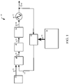
- FIG. 1 shows an embodiment 10 of PLL for generating a radar chirp.
- the embodiment 10 includes a VCO 12 for generating a VCO frequency (F VCO ) 14.
- the VCO frequency 14 is divided by a frequency divider 16 to generate a divided frequency 18.
- a reference frequency circuit 20 generates a reference frequency 22.
- the reference frequency circuit 20 includes a crystal oscillator followed by a buffer. In another embodiment, the crystal oscillator is replaced with a digital waveform generator.
- a phase frequency detector 24 compares the divided frequency 18 with the reference frequency 22 to determine a difference 26.
- the difference 26 is a pulse width proportional to a phase difference between the divided frequency 18 and the reference frequency 22.
- a charge pump 28 generates a charge pump voltage 30 in response to the difference 26.
- a low pass filter 32 generates a filtered output voltage 34 based on the charge pump voltage 30.
- the VCO 12 generates the VCO frequency 14 based on the filtered output voltage 34.
- a digital controller 36 generates control signals 38 to change a division ratio of the frequency divider 16. For example, if the division ratio is ten, the VCO frequency 14 will be generated to have a frequency ten times greater than the reference frequency 22.
- the frequency divider 16 is a cascaded series of D-flip flops, configured to divide the VCO frequency 14 by binary multiples.
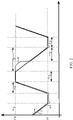
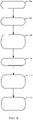
- FIG. 2 is a graphical view comparing an ideal FMCW 40 to an actual FMCW 42 where the frequency undershoot and linearity of the chirp phase are poorly controlled by the embodiment 10 of FIG. 1 .
- the ideal FMCW 40 spans a frequency range from a stop frequency (F1) 44 to a start frequency 46.
- the FMCW waveforms 40 and 42 consist of a Time Ramp Slope Return (T RSR or "return phase") 50, a stop frequency time (T1) 52, a Time Ramp Slope Data (T RSD or "chirp phase") 54, and a stop frequency time (T2) 56.
- T RSR Time Ramp Slope Return
- T1 Stop frequency time
- T RSD Time Ramp Slope Data
- T2 Stop frequency time
- the embodiment 70 includes a low pass filter 72 configured to receive a phase preset current, described in further detail in FIG. 4 .
- the low pass filter 72 generates a filtered output voltage 74, which controls the VCO 12 and is measured by a measurement circuit 76 to generate a measured value 78.
- the measurement circuit 76 determines the measured value 78 during a startup phase of the PLL.
- the measurement circuit 76 stores the measured value 78 in a register of a phase preset calibration circuit 80, included in the digital controller 82.
- the measured value 78 is calculated periodically, to improve accuracy due to component drift and aging.
- the phase preset calibration circuit 80 generates a calibration current control signal provided to the phase preset circuit 86 through a connection 84.
- the calibration current is determined during a calibration, and in response to the measurement circuit 76.
- the phase preset circuit 86 supplies the calibration current over a connection 88 to the low pass filter 72, during the calibration.
- the digital controller 82 generates a set of phase preset current control signals provided to the phase preset circuit 86 through a connection 94.
- the phase preset circuit 86 supplies the phase preset current to the low pass filter 72 through a connection 98.
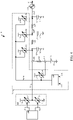
- FIG. 4 shows additional detail of an embodiment 100 where the connections 88 and 98 of FIG. 3 are combined to carry either the calibration current or the phase preset current.
- the embodiment 100 includes a VCO 102 configured to generate an FMCW 104.
- a phase frequency detector 106 provides a charge pump 108 a pair of differential difference signals 120 and 122 that measure a phase difference between a reference frequency and a divided FMCW 104.
- the differential signals 120 and 122 enable a respective current source 124 and 126, connected in series between a supply rail 130 and a ground 132, to provide a respective positive or negative pulse for the charge pump voltage 134.
- the embodiment 100 shows a configuration of resistive and capacitive elements to provide low pass filtering. It should be understood that other numbers and arrangements of components also provide low pass filtering appropriate to the design goals (e.g., bandwidth, and response time), of the PLL.
- a first resistor 140 is connected between two external pins 142 and 144.
- a first capacitor 146 is connected between the external pin 144 and the ground 132. In the embodiment 100, the first resistor 140 and the first capacitor 146 are external to an integrated PLL due to their physical size.
- a second capacitor 150 is connected between the charge pump voltage 134 and the ground 132.
- a second resistor 152 is connected between a node 154 and the ground 132.
- a third capacitor 156 is connected between the node 154 and the ground 132.
- a third resistor 158 is connected between the filtered output voltage 160 and the node 154.
- a fourth capacitor 162 is connected between the filtered output voltage 160 and the ground 132.
- a group of phase preset related circuits 170 includes a phase preset circuit 172, receiving a phase preset current control signal (I PHC ) 178 and a calibration current control signal (I CAL ) 176.
- the phase preset circuit 172 supplies the calibration current control signal to the node 174 during calibration (e.g., during a startup phase of the PLL), and supplies the phase preset current control signal to the node 174 during a start frequency time preceding the chirp phase.
- the control signals from the phase preset circuit 172 controls current sources 190, 192, 194 and 196, which supply current to respective capacitors 146, 150, 156 and 162.
- the calibration techniques described herein are applied to different loop filter configurations.
- the loop filter is fully integrated with the other circuits shown in FIG. 3 , or the loop filter is external to a monolithic substrate including the other circuits or FIG. 3 , or the loop filter is integrated as a multichip module or hybrid is the other circuits of FIG. 3 .
- the PLL includes the charge pump and loop filter with a different type and/or order than shown in FIG. 3 , wherein the PLL bandwidth and chirp ramp slope are not correlated.
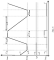
- FIG. 5 shows various operational waveforms, for the embodiment 70 of FIG. 3 .
- the FMCW 200 transitions between a start frequency 202 and a stop frequency 204.
- the FMCW 200 includes a return phase (T RSR ) 300, a start frequency time (T1) 302, a chirp phase (T RSD ) 304 and an end frequency time 306.
- T RSR return phase
- T1 start frequency time
- T RSD chirp phase
- end frequency time 306 the charge pump current
- I PHC phase preset current
- the FMCW chirp has a non-linear shape during the chirp time 304 (e.g., a Frequency Shift Key (FSK) FMCW chirp).
- FSK Frequency Shift Key
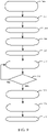
- FIG. 6 and FIG. 7 compare experimental results with and without the use of the phase preset compensation for the low pass filter of the PLL.
- FIG. 6 shows an ideal FMCW 320 during the return phase 300, the start frequency time 302 and the chirp phase 304.
- a traditional FMCW 322 shows poor linearity during the first part of the chirp phase 304 as well as a significant frequency overshoot that extends well into the start frequency time 302.
- FIG. 7 shows an FMCW 332 closely tracking the ideal FMCW 320 during the chirp phase 304 when phase preset compensation is applied to the low pass filter of the PLL.
- FIG. 8 shows a method for presetting a phase for a fast chirp PLL.
- an FMCW 14 is generated with a VCO 12.
- the FMCW 14 is divided with a frequency divider 16.
- a charge pump voltage 30 is generated in response to a difference 26 between a reference waveform 22 and a divided FMCW 18.
- the charge pump voltage 30 is filtered with a filter 72.
- the frequency divider 16 is modified with a digital controller 82, to generate a chirp phase 304 and a return phase 300.
- a phase preset current 98 is supplied to the filter 72 with a phase preset circuit 86, during a start frequency time 302 preceding the chirp phase 304.
- FIG. 9 shows a method for presetting a phase for a fast chirp PLL, wherein a phase preset current supplied during a time preceding the chirp phase is a function of a predetermined current value during a calibration phase.
- values for Fstart 202, Fstop 204, T RSR 300 and T RSD 304 are set in a register included in the phase preset calibration circuit 80.
- these values are written into the phase preset calibration circuit 80 through a serial port interface (SPI).
- SPI serial port interface
- these values are written into the digital controller 82, and are accessible to the phase preset calibration circuit 80.
- a counter (CNT_VAL) for a number of clock cycles is also cleared, or set to zero at 360. In other embodiments, the counter is cleared in one of 362, 364, 366 and 368.
- the PLL frequency (e.g., FMCW) 14 is set to Fstart 202.
- the filtered output voltage 74 is measured by the measurement circuit 76 to determine Vstart.
- the PLL frequency 14 is set to Fstop 204 by appropriate selection of the division ratio in the frequency divider 16.
- the filtered output voltage 74 is measured again with the measurement circuit 76 to determine Vstop.
- the charge pump 28 is disabled.
- a calibration current (I CAL ) 88 is supplied to the filter 72 and the counter is incremented.
- the method proceeds to 374, otherwise the method returns to 370.
- an elapsed time (dT) is calculated as the counter value (e.g., number of clock cycles) multiplied by the clock period (Tclk).
- the phase preset current (I PHC ) is calculated to be equal to the calibration current (I CAL ), multiplied by the elapsed time (dT), divided by the duration of the chirp phase (T RSD ) 304.
- the calculation of the elapsed time and the phase preset current is calculated with a circuit in the digital controller 82. In another embodiment, the calculation of the elapsed time and the phase preset current is calculated with software and registers in the digital controller 82. At 378, the charge pump 28 is reactivated, so that chirp transmission can subsequently occur.
- a fast chirp Phase Locked Loop (PLL) with phase preset comprises a Voltage Controlled Oscillator (VCO) configured to generate a Frequency Modulated Continuous Waveform (FMCW).
- VCO Voltage Controlled Oscillator
- FMCW Frequency Modulated Continuous Waveform
- the VCO is responsive to a filtered output voltage of a filter connected to a charge pump.
- the charge pump is responsive to a difference between a reference frequency waveform and a divided frequency waveform generated by a frequency divider configured to divide the FMCW.
- a digital controller is connected to the frequency divider and is configured to modify a division ratio of the frequency divider to generate a chirp phase and a return phase.
- the chirp phase includes a first linear change of the FMCW from a start frequency to a stop frequency.
- the return phase includes a second linear change of the FMCW from the stop frequency to the start frequency.
- a phase preset circuit is connected to the digital controller and the filter. The phase preset circuit supplies a phase preset current during a start frequency time preceding the chirp phase. The phase preset current is proportional to a VCO gain of the VCO and inversely proportional to a chirp current during the chirp phase.
- phase preset current is determined by a calibration circuit including a counter configured to determine a number of clock cycles elapsed during a change from the stop frequency to the start frequency by measuring the filtered output voltage, storing the number of clock cycles in the digital controller and controlling the phase preset circuit with the digital controller to supply the phase preset current.
- the phase preset current is determined by multiplying a calibration current, supplied by the phase preset circuit to the filter, by the number of clock cycles, multiplied by a clock period, and divided by a duration of the return phase.
- the phase preset current is determined during a startup phase of the PLL.
- the filter is a low pass filter comprising a plurality of filter stages.
- the phase preset current is distributed to each of the plurality of filter stages.
- the FMCW is a down-chirp waveform, wherein the start frequency is greater than the stop frequency. Without the phase preset current, the PLL has a reduction in a usable chirp phase.
- a method for presetting a phase of a fast chirp Phase Locked Loop comprises generating a Frequency Modulated Continuous Waveform (FMCW) with a Voltage Controlled Oscillator (VCO).
- the VCO responds to a filtered output voltage.
- the FMCW is divided with a frequency divider to generate a divided frequency waveform.
- a charge pump voltage is generated in response to a difference between a reference frequency waveform and the divided frequency waveform.
- the charge pump voltage is filtered with a filter, to generate the filtered output voltage.
- a digital controller modifies a division ratio of the frequency divider to generate a chirp phase and a return phase.
- the chirp phase includes a first linear change of the FMCW from a start frequency to a stop frequency.
- the return phase includes a second linear change of the FMCW from the stop frequency to the start frequency.
- a phase preset circuit supplies a phase preset current to the filter during a start frequency time preceding the chirp phase, wherein the phase preset current is proportional to a VCO gain of the VCO and inversely proportional to a chirp current during the chirp phase.
- phase preset current is determined by counting, with a calibration circuit, a number of clock cycles elapsed during a change from the stop frequency to the start frequency by measuring the filtered output voltage, storing the number of clock cycles in the digital controller and controlling the phase preset circuit with the digital controller to supply the phase preset current.
- the phase preset current is determined by multiplying a calibration current, supplied by the phase preset circuit to the filter, by the number of clock cycles, multiplied by a clock period, and divided by a duration of the chirp phase.
- the phase preset current is determined during a startup phase of the PLL.
- Filtering the charge pump voltage comprises filtering with a low pass filter comprising a plurality of filter stages.
- the phase preset current is distributed to each of the plurality of filter stages.
- the phase preset circuit is controlled with the digital controller during the start frequency time. The bandwidth of the PLL is limited to minimize a phase noise.
- a method for presetting a phase of a fast chirp Phase Locked Loop comprises generating a Frequency Modulated Continuous Waveform (FMCW) with the PLL.
- the PLL includes a low pass filter configured to generate a filtered output voltage by filtering a charge pump voltage of a charge pump.
- the charge pump is responsive to a difference between a divided FMCW and a reference frequency waveform.
- the FMCW includes a chirp phase and a return phase.
- the chirp phase includes a first linear change of the FMCW from a start frequency to a stop frequency.
- the return phase includes a second linear change of the FMCW from the stop frequency to the start frequency.
- a phase preset current is supplied to the low pass filter during a start frequency time preceding the chirp phase, wherein determining the phase preset current comprises: measuring a start voltage from the filtered output voltage while an FMCW frequency is equal to the start frequency, setting the FMCW frequency to the stop frequency, wherein the filtered output voltage equals a stop voltage, disabling the charge pump, supplying a calibration current to the low pass filter, and counting a number of clock cycles elapsed during a change from the stop voltage to the start voltage, wherein each clock cycle has a clock period, setting the phase preset current equal to the calibration current multiplied by the number of clock cycles, multiplied by the clock period, and divided by a duration of the chirp phase, and enabling the charge pump, and supplying the phase preset current during a subsequent start frequency time.
- phase preset current is determined during a startup phase.
- the calibration current is supplied to the low pass filter during a startup phase, and the phase preset current is supplied to the low pass filter during the start frequency time. Without the phase preset current, the PLL has a reduction in a usable chirp time.
Landscapes
- Engineering & Computer Science (AREA)
- Radar, Positioning & Navigation (AREA)
- Remote Sensing (AREA)
- Computer Networks & Wireless Communication (AREA)
- Physics & Mathematics (AREA)
- General Physics & Mathematics (AREA)
- Stabilization Of Oscillater, Synchronisation, Frequency Synthesizers (AREA)
Claims (10)
- Schneller Chirp-Phasenregelkreis, PLL, (70) mit Phasenvoreinstellung, der Folgendes umfasst:einen spannungsgesteuerten Oszillator, VCO, (12), der konfiguriert ist, eine frequenzmodulierte Dauerstrich-Wellenform, FMCW, (14) zu erzeugen, wobei der VCO auf eine gefilterte Ausgangsspannung (74) eines Filters (72), das mit einer Ladungspumpe (28) verbunden ist, reagiert, wobei die Ladungspumpe auf einen Unterschied zwischen einer Referenzfrequenzwellenform (22) und einer geteilten Frequenzwellenform (18), die durch einen Frequenzteiler (16) erzeugt wird, der konfiguriert ist, die FMCW zu teilen, reagiert;eine digitale Steuereinheit (82), die mit dem Frequenzteiler verbunden ist und konfiguriert ist, ein Unterteilungsverhältnis des Frequenzteilers zu ändern, um eine Chirp-Phase (304) und eine Rücklaufphase (300) zu erzeugen, wobei die Chirp-Phase eine erste lineare Änderung der FMCW von einer Startfrequenz (202) zu einer Stoppfrequenz (204) enthält und die Rücklaufphase eine zweite lineare Änderung der FMCW von der Stoppfrequenz zu der Startfrequenz enthält, gekennzeichnet durch:
eine Phasenvoreinstellungsschaltung (86), die mit der digitalen Steuereinheit und dem Filter verbunden ist, wobei die Phasenvoreinstellungsschaltung einen Phasenvoreinstellungsstrom (98) während einer Startfrequenzzeit (302), die der Chirp-Phase vorausgeht, liefert, wobei der Phasenvoreinstellungsstrom proportional zu einer VCO-Verstärkung des VCO und umgekehrt proportional zu einem Chirp-Strom während der Chirp-Phase ist. - PLL nach Anspruch 1, wobei der Phasenvoreinstellungsstrom durch eine Kalibrierungsschaltung (80), die einen Zähler enthält, der konfiguriert ist, eine Anzahl von Taktzyklen zu bestimmen, die während einer Änderung von der Stoppfrequenz zu der Startfrequenz vergangen sind, durch Messen der gefilterten Ausgangsspannung, Speichern der Anzahl von Taktzyklen in der digitalen Steuereinheit und Steuern der Phasenvoreinstellungsschaltung mit der digitalen Steuereinheit, um den Phasenvoreinstellungsstrom zu liefern, bestimmt wird.
- PLL nach Anspruch 2, wobei der Phasenvoreinstellungsstrom durch Multiplizieren eines Kalibrierungsstroms (88), der durch die Phasenvoreinstellungsschaltung an das Filter geliefert wird, mit der Anzahl von Taktzyklen multipliziert mit einer Taktperiode und geteilt durch eine Dauer der Chirp-Phase bestimmt wird.
- PLL nach Anspruch 1, wobei das Filter ein Tiefpassfilter ist, das mehrere Filterstufen umfasst.
- PLL nach Anspruch 4, wobei der Phasenvoreinstellungsstrom an jede der mehreren Filterstufen verteilt wird.
- Verfahren zum Voreinstellen einer Phase eines schnellen Chirp-Phasenregelkreises, PLL, (70), das Folgendes umfasst:Erzeugen (340) einer frequenzmodulierten Dauerstrich-Wellenform, FMCW, (14) mit einem spannungsgesteuerten Oszillator, VCO, (12), wobei der VCO auf eine gefilterte Ausgangsspannung (74) reagiert;Teilen (342) der FMCW mit einem Frequenzteiler (16), um eine geteilte Frequenzwellenform (18) zu erzeugen;Erzeugen (344) einer Ladungspumpenspannung (30) als Reaktion auf einen Unterschied zwischen einer Referenzfrequenzwellenform (22) und der geteilten Frequenzwellenform;Filtern (346) der Ladungspumpenspannung mit einem Filter (72), um die gefilterte Ausgangsspannung zu erzeugen;Ändern (348) mit einer digitalen Steuereinheit (82) eines Teilungsverhältnisses des Frequenzteilers, um eine Chirp-Phase (304) und eine Rücklaufphase (300) zu erzeugen, wobei die Chirp-Phase eine erste lineare Änderung der FMCW von einer Startfrequenz (202) zu einer Stoppfrequenz (204) enthält und die Rücklaufphase eine zweite lineare Änderung der FMCW von der Stoppfrequenz zu der Startfrequenz enthält; und gekennzeichnet durch:
Liefern (350) mit einer Phasenvoreinstellungsschaltung (86) eines Phasenvoreinstellungsstroms (98) an das Filter während einer Startfrequenzzeit (302), die der Chirp-Phase vorausgeht, wobei der Phasenvoreinstellungsstrom proportional zu einer VCO-Verstärkung des VCO und umgekehrt proportional zu einem Chirp-Strom während der Chirp-Phase ist. - Verfahren nach Anspruch 6, das ferner umfasst, den Phasenvoreinstellungsstrom durch Zählen mit einer Kalibrierungsschaltung (80) einer Anzahl von Taktzyklen, die während einer Änderung von der Stoppfrequenz zu der Startfrequenz vergangen sind, durch Messen der gefilterten Ausgangsspannung, Speichern der Anzahl von Taktzyklen in der digitalen Steuereinheit und Steuern der Phasenvoreinstellungsschaltung mit der digitalen Steuereinheit, um den Phasenvoreinstellungsstrom zu liefern, zu bestimmen.
- Verfahren nach Anspruch 7, das ferner umfasst, den Phasenvoreinstellungsstrom durch Multiplizieren eines Kalibrierungsstroms (88), der durch die Phasenvoreinstellungsschaltung an das Filter geliefert wird, mit der Anzahl von Taktzyklen multipliziert mit einer Taktperiode und geteilt durch eine Dauer der Chirp-Phase zu bestimmen.
- Verfahren nach Anspruch 6, wobei das Filtern der Ladungspumpenspannung umfasst, mit einem Tiefpassfilter, das mehrere Filterstufen umfasst, zu filtern.
- Verfahren nach Anspruch 9, das ferner umfasst, den Phasenvoreinstellungsstrom an jede der mehreren Filterstufen zu verteilen.
Priority Applications (3)
| Application Number | Priority Date | Filing Date | Title |
|---|---|---|---|
| EP18305690.2A EP3579012B1 (de) | 2018-06-06 | 2018-06-06 | Phasenvoreinstellung für schnellen chirp-phasenregelkreis |
| US16/426,638 US11131763B2 (en) | 2018-06-06 | 2019-05-30 | Phase preset for fast chirp PLL |
| CN201910475001.4A CN110572153B (zh) | 2018-06-06 | 2019-05-31 | 用于快速啁啾pll的相位预设 |
Applications Claiming Priority (1)
| Application Number | Priority Date | Filing Date | Title |
|---|---|---|---|
| EP18305690.2A EP3579012B1 (de) | 2018-06-06 | 2018-06-06 | Phasenvoreinstellung für schnellen chirp-phasenregelkreis |
Publications (2)
| Publication Number | Publication Date |
|---|---|
| EP3579012A1 EP3579012A1 (de) | 2019-12-11 |
| EP3579012B1 true EP3579012B1 (de) | 2022-03-30 |
Family
ID=62715985
Family Applications (1)
| Application Number | Title | Priority Date | Filing Date |
|---|---|---|---|
| EP18305690.2A Active EP3579012B1 (de) | 2018-06-06 | 2018-06-06 | Phasenvoreinstellung für schnellen chirp-phasenregelkreis |
Country Status (3)
| Country | Link |
|---|---|
| US (1) | US11131763B2 (de) |
| EP (1) | EP3579012B1 (de) |
| CN (1) | CN110572153B (de) |
Cited By (1)
| Publication number | Priority date | Publication date | Assignee | Title |
|---|---|---|---|---|
| EP4614817A4 (de) * | 2022-11-04 | 2025-12-10 | Calterah Semiconductor Tech Shanghai Co Ltd | Phasenregelkreis, hochfrequenzsignalsender, radarsensor und elektronische vorrichtung |
Families Citing this family (4)
| Publication number | Priority date | Publication date | Assignee | Title |
|---|---|---|---|---|
| US11228318B1 (en) | 2020-10-29 | 2022-01-18 | Nxp B.V. | Bandwidth adjustability in an FMCW PLL system |
| US11789137B2 (en) | 2020-12-30 | 2023-10-17 | Texas Instruments Incorporated | FMCW chirp bandwidth control |
| US12523745B2 (en) * | 2022-06-22 | 2026-01-13 | Nxp B.V. | Injection current modulation for chirp signal timing control |
| CN117418925B (zh) * | 2023-12-19 | 2024-02-13 | 四川智感蔚蓝科技有限公司 | 一种氮氧传感器的泵氧控制方法、装置、介质和设备 |
Family Cites Families (14)
| Publication number | Priority date | Publication date | Assignee | Title |
|---|---|---|---|---|
| US6046646A (en) * | 1997-06-13 | 2000-04-04 | Lo; Pedro W. | Modulation of a phase locked loop for spreading the spectrum of an output clock signal |
| CA2281522C (en) | 1999-09-10 | 2004-12-07 | Philsar Electronics Inc. | Delta-sigma based two-point angle modulation scheme |
| US8085097B2 (en) | 2008-05-06 | 2011-12-27 | Hittite Microwave Corporation | Integrated ramp, sweep fractional frequency synthesizer on an integrated circuit chip |
| JP2010071899A (ja) | 2008-09-19 | 2010-04-02 | Toshiba Corp | Fmcw信号生成器及びそれを用いたレーダ装置 |
| WO2010092438A1 (en) | 2009-02-13 | 2010-08-19 | Freescale Semiconductor, Inc. | Integrated circuit comprising frequency generation circuitry for controlling a frequency source |
| US9515666B2 (en) | 2014-08-27 | 2016-12-06 | Freescale Semiconductor, Inc. | Method for re-centering a VCO, integrated circuit and wireless device |
| EP3059866A1 (de) * | 2015-02-17 | 2016-08-24 | Nxp B.V. | Zwei-Punkt-Modulation einer Halbdigitalen Phasenregelschleife |
| EP3059857B1 (de) * | 2015-02-17 | 2021-11-03 | Nxp B.V. | Zeit-Digital-Wandler und Phasenregelschleife |
| EP3096160B1 (de) * | 2015-05-20 | 2020-02-26 | Veoneer Sweden AB | Fmcw-kraftfahrzeug-radarsystem |
| DE112015006867B4 (de) * | 2015-10-01 | 2019-03-28 | Mitsubishi Electric Corporation | Signalgenerator |
| US10659062B2 (en) * | 2016-12-15 | 2020-05-19 | Mitsubishi Electric Corporation | PLL circuit |
| DE102017124343B4 (de) * | 2016-12-16 | 2021-04-08 | Infineon Technologies Ag | Erzeugung schneller frequenzrampen |
| JP6494888B2 (ja) * | 2016-12-19 | 2019-04-03 | 三菱電機株式会社 | Pll回路 |
| CN107727612A (zh) * | 2017-11-03 | 2018-02-23 | 李俊 | 基于啁啾色散光谱的可燃及有毒气体泄漏监测检测装置及方法 |
-
2018
- 2018-06-06 EP EP18305690.2A patent/EP3579012B1/de active Active
-
2019
- 2019-05-30 US US16/426,638 patent/US11131763B2/en active Active
- 2019-05-31 CN CN201910475001.4A patent/CN110572153B/zh active Active
Cited By (1)
| Publication number | Priority date | Publication date | Assignee | Title |
|---|---|---|---|---|
| EP4614817A4 (de) * | 2022-11-04 | 2025-12-10 | Calterah Semiconductor Tech Shanghai Co Ltd | Phasenregelkreis, hochfrequenzsignalsender, radarsensor und elektronische vorrichtung |
Also Published As
| Publication number | Publication date |
|---|---|
| CN110572153B (zh) | 2024-09-10 |
| US20190377076A1 (en) | 2019-12-12 |
| EP3579012A1 (de) | 2019-12-11 |
| US11131763B2 (en) | 2021-09-28 |
| CN110572153A (zh) | 2019-12-13 |
Similar Documents
| Publication | Publication Date | Title |
|---|---|---|
| US11131763B2 (en) | Phase preset for fast chirp PLL | |
| US11131762B2 (en) | Boosted return time for fast chirp PLL and calibration method | |
| US10382045B2 (en) | Digital phase locked loops | |
| US10284209B2 (en) | Phase locked loop | |
| US9007109B2 (en) | Automatic loop-bandwidth calibration for a digital phased-locked loop | |
| JP6494888B2 (ja) | Pll回路 | |
| US11418204B2 (en) | Phase lock loop (PLL) with operating parameter calibration circuit and method | |
| US10236899B1 (en) | Tunable fractional phase locked loop | |
| PL195271B1 (pl) | Sposób i układ strojenia szerokości pasma pętli fazowej | |
| US9722617B2 (en) | Phase locked loop and associated method for loop gain calibration | |
| US7023285B2 (en) | Self-calibrating controllable oscillator | |
| EP4296717B1 (de) | Injektionsstrommodulation für chirpsignalzeitsteuerung | |
| US9712174B1 (en) | Double calibration loop for random spread spectrum modulator | |
| GB2519417A (en) | Radar apparatus and method | |
| GB2547551A (en) | An electronic circuit | |
| US8502588B2 (en) | Clock generation system | |
| KR20180057508A (ko) | 주파수 변조 연속파 생성기 및 이를 포함하는 주파수 변조 연속파 레이더 시스템 | |
| EP3489711A1 (de) | Fll für ein frequenzmoduliertes dauerstrichradar | |
| US8773181B2 (en) | Locked loop circuits and methods | |
| US7671690B2 (en) | Method and signal control system providing fast transitions in an oscillating signal | |
| CN117674829A (zh) | 锁相环控制方法、系统、雷达及介质 | |
| US20110090109A1 (en) | Charge pump |
Legal Events
| Date | Code | Title | Description |
|---|---|---|---|
| STAA | Information on the status of an ep patent application or granted ep patent |
Free format text: STATUS: UNKNOWN |
|
| PUAI | Public reference made under article 153(3) epc to a published international application that has entered the european phase |
Free format text: ORIGINAL CODE: 0009012 |
|
| STAA | Information on the status of an ep patent application or granted ep patent |
Free format text: STATUS: THE APPLICATION HAS BEEN PUBLISHED |
|
| AK | Designated contracting states |
Kind code of ref document: A1 Designated state(s): AL AT BE BG CH CY CZ DE DK EE ES FI FR GB GR HR HU IE IS IT LI LT LU LV MC MK MT NL NO PL PT RO RS SE SI SK SM TR |
|
| AX | Request for extension of the european patent |
Extension state: BA ME |
|
| STAA | Information on the status of an ep patent application or granted ep patent |
Free format text: STATUS: REQUEST FOR EXAMINATION WAS MADE |
|
| 17P | Request for examination filed |
Effective date: 20200612 |
|
| RBV | Designated contracting states (corrected) |
Designated state(s): AL AT BE BG CH CY CZ DE DK EE ES FI FR GB GR HR HU IE IS IT LI LT LU LV MC MK MT NL NO PL PT RO RS SE SI SK SM TR |
|
| GRAJ | Information related to disapproval of communication of intention to grant by the applicant or resumption of examination proceedings by the epo deleted |
Free format text: ORIGINAL CODE: EPIDOSDIGR1 |
|
| GRAP | Despatch of communication of intention to grant a patent |
Free format text: ORIGINAL CODE: EPIDOSNIGR1 |
|
| RIC1 | Information provided on ipc code assigned before grant |
Ipc: G01S 13/28 20060101ALN20211007BHEP Ipc: H03L 7/22 20060101ALI20211007BHEP Ipc: H03L 7/18 20060101ALI20211007BHEP Ipc: H03L 7/089 20060101ALI20211007BHEP Ipc: H03C 3/09 20060101ALI20211007BHEP Ipc: H03B 1/04 20060101ALI20211007BHEP Ipc: H03L 7/093 20060101ALI20211007BHEP Ipc: G01S 13/93 20200101ALI20211007BHEP Ipc: G01S 13/34 20060101ALI20211007BHEP Ipc: G01S 7/40 20060101ALI20211007BHEP Ipc: G01S 7/35 20060101ALI20211007BHEP Ipc: G01S 7/03 20060101AFI20211007BHEP |
|
| GRAP | Despatch of communication of intention to grant a patent |
Free format text: ORIGINAL CODE: EPIDOSNIGR1 |
|
| STAA | Information on the status of an ep patent application or granted ep patent |
Free format text: STATUS: GRANT OF PATENT IS INTENDED |
|
| RIC1 | Information provided on ipc code assigned before grant |
Ipc: G01S 13/28 20060101ALN20211112BHEP Ipc: H03L 7/22 20060101ALI20211112BHEP Ipc: H03L 7/18 20060101ALI20211112BHEP Ipc: H03L 7/089 20060101ALI20211112BHEP Ipc: H03C 3/09 20060101ALI20211112BHEP Ipc: H03B 1/04 20060101ALI20211112BHEP Ipc: H03L 7/093 20060101ALI20211112BHEP Ipc: G01S 13/93 20200101ALI20211112BHEP Ipc: G01S 13/34 20060101ALI20211112BHEP Ipc: G01S 7/40 20060101ALI20211112BHEP Ipc: G01S 7/35 20060101ALI20211112BHEP Ipc: G01S 7/03 20060101AFI20211112BHEP |
|
| INTG | Intention to grant announced |
Effective date: 20211209 |
|
| GRAS | Grant fee paid |
Free format text: ORIGINAL CODE: EPIDOSNIGR3 |
|
| GRAA | (expected) grant |
Free format text: ORIGINAL CODE: 0009210 |
|
| STAA | Information on the status of an ep patent application or granted ep patent |
Free format text: STATUS: THE PATENT HAS BEEN GRANTED |
|
| AK | Designated contracting states |
Kind code of ref document: B1 Designated state(s): AL AT BE BG CH CY CZ DE DK EE ES FI FR GB GR HR HU IE IS IT LI LT LU LV MC MK MT NL NO PL PT RO RS SE SI SK SM TR |
|
| REG | Reference to a national code |
Ref country code: GB Ref legal event code: FG4D |
|
| REG | Reference to a national code |
Ref country code: CH Ref legal event code: EP |
|
| REG | Reference to a national code |
Ref country code: DE Ref legal event code: R096 Ref document number: 602018032912 Country of ref document: DE |
|
| REG | Reference to a national code |
Ref country code: AT Ref legal event code: REF Ref document number: 1479699 Country of ref document: AT Kind code of ref document: T Effective date: 20220415 |
|
| REG | Reference to a national code |
Ref country code: IE Ref legal event code: FG4D |
|
| REG | Reference to a national code |
Ref country code: LT Ref legal event code: MG9D |
|
| PG25 | Lapsed in a contracting state [announced via postgrant information from national office to epo] |
Ref country code: SE Free format text: LAPSE BECAUSE OF FAILURE TO SUBMIT A TRANSLATION OF THE DESCRIPTION OR TO PAY THE FEE WITHIN THE PRESCRIBED TIME-LIMIT Effective date: 20220330 Ref country code: RS Free format text: LAPSE BECAUSE OF FAILURE TO SUBMIT A TRANSLATION OF THE DESCRIPTION OR TO PAY THE FEE WITHIN THE PRESCRIBED TIME-LIMIT Effective date: 20220330 Ref country code: NO Free format text: LAPSE BECAUSE OF FAILURE TO SUBMIT A TRANSLATION OF THE DESCRIPTION OR TO PAY THE FEE WITHIN THE PRESCRIBED TIME-LIMIT Effective date: 20220630 Ref country code: LT Free format text: LAPSE BECAUSE OF FAILURE TO SUBMIT A TRANSLATION OF THE DESCRIPTION OR TO PAY THE FEE WITHIN THE PRESCRIBED TIME-LIMIT Effective date: 20220330 Ref country code: HR Free format text: LAPSE BECAUSE OF FAILURE TO SUBMIT A TRANSLATION OF THE DESCRIPTION OR TO PAY THE FEE WITHIN THE PRESCRIBED TIME-LIMIT Effective date: 20220330 Ref country code: BG Free format text: LAPSE BECAUSE OF FAILURE TO SUBMIT A TRANSLATION OF THE DESCRIPTION OR TO PAY THE FEE WITHIN THE PRESCRIBED TIME-LIMIT Effective date: 20220630 |
|
| REG | Reference to a national code |
Ref country code: NL Ref legal event code: MP Effective date: 20220330 |
|
| REG | Reference to a national code |
Ref country code: AT Ref legal event code: MK05 Ref document number: 1479699 Country of ref document: AT Kind code of ref document: T Effective date: 20220330 |
|
| PG25 | Lapsed in a contracting state [announced via postgrant information from national office to epo] |
Ref country code: LV Free format text: LAPSE BECAUSE OF FAILURE TO SUBMIT A TRANSLATION OF THE DESCRIPTION OR TO PAY THE FEE WITHIN THE PRESCRIBED TIME-LIMIT Effective date: 20220330 Ref country code: GR Free format text: LAPSE BECAUSE OF FAILURE TO SUBMIT A TRANSLATION OF THE DESCRIPTION OR TO PAY THE FEE WITHIN THE PRESCRIBED TIME-LIMIT Effective date: 20220701 Ref country code: FI Free format text: LAPSE BECAUSE OF FAILURE TO SUBMIT A TRANSLATION OF THE DESCRIPTION OR TO PAY THE FEE WITHIN THE PRESCRIBED TIME-LIMIT Effective date: 20220330 |
|
| PG25 | Lapsed in a contracting state [announced via postgrant information from national office to epo] |
Ref country code: NL Free format text: LAPSE BECAUSE OF FAILURE TO SUBMIT A TRANSLATION OF THE DESCRIPTION OR TO PAY THE FEE WITHIN THE PRESCRIBED TIME-LIMIT Effective date: 20220330 |
|
| PG25 | Lapsed in a contracting state [announced via postgrant information from national office to epo] |
Ref country code: SM Free format text: LAPSE BECAUSE OF FAILURE TO SUBMIT A TRANSLATION OF THE DESCRIPTION OR TO PAY THE FEE WITHIN THE PRESCRIBED TIME-LIMIT Effective date: 20220330 Ref country code: SK Free format text: LAPSE BECAUSE OF FAILURE TO SUBMIT A TRANSLATION OF THE DESCRIPTION OR TO PAY THE FEE WITHIN THE PRESCRIBED TIME-LIMIT Effective date: 20220330 Ref country code: RO Free format text: LAPSE BECAUSE OF FAILURE TO SUBMIT A TRANSLATION OF THE DESCRIPTION OR TO PAY THE FEE WITHIN THE PRESCRIBED TIME-LIMIT Effective date: 20220330 Ref country code: PT Free format text: LAPSE BECAUSE OF FAILURE TO SUBMIT A TRANSLATION OF THE DESCRIPTION OR TO PAY THE FEE WITHIN THE PRESCRIBED TIME-LIMIT Effective date: 20220801 Ref country code: ES Free format text: LAPSE BECAUSE OF FAILURE TO SUBMIT A TRANSLATION OF THE DESCRIPTION OR TO PAY THE FEE WITHIN THE PRESCRIBED TIME-LIMIT Effective date: 20220330 Ref country code: EE Free format text: LAPSE BECAUSE OF FAILURE TO SUBMIT A TRANSLATION OF THE DESCRIPTION OR TO PAY THE FEE WITHIN THE PRESCRIBED TIME-LIMIT Effective date: 20220330 Ref country code: CZ Free format text: LAPSE BECAUSE OF FAILURE TO SUBMIT A TRANSLATION OF THE DESCRIPTION OR TO PAY THE FEE WITHIN THE PRESCRIBED TIME-LIMIT Effective date: 20220330 Ref country code: AT Free format text: LAPSE BECAUSE OF FAILURE TO SUBMIT A TRANSLATION OF THE DESCRIPTION OR TO PAY THE FEE WITHIN THE PRESCRIBED TIME-LIMIT Effective date: 20220330 |
|
| PG25 | Lapsed in a contracting state [announced via postgrant information from national office to epo] |
Ref country code: PL Free format text: LAPSE BECAUSE OF FAILURE TO SUBMIT A TRANSLATION OF THE DESCRIPTION OR TO PAY THE FEE WITHIN THE PRESCRIBED TIME-LIMIT Effective date: 20220330 Ref country code: IS Free format text: LAPSE BECAUSE OF FAILURE TO SUBMIT A TRANSLATION OF THE DESCRIPTION OR TO PAY THE FEE WITHIN THE PRESCRIBED TIME-LIMIT Effective date: 20220730 Ref country code: AL Free format text: LAPSE BECAUSE OF FAILURE TO SUBMIT A TRANSLATION OF THE DESCRIPTION OR TO PAY THE FEE WITHIN THE PRESCRIBED TIME-LIMIT Effective date: 20220330 |
|
| REG | Reference to a national code |
Ref country code: DE Ref legal event code: R097 Ref document number: 602018032912 Country of ref document: DE |
|
| PG25 | Lapsed in a contracting state [announced via postgrant information from national office to epo] |
Ref country code: MC Free format text: LAPSE BECAUSE OF FAILURE TO SUBMIT A TRANSLATION OF THE DESCRIPTION OR TO PAY THE FEE WITHIN THE PRESCRIBED TIME-LIMIT Effective date: 20220330 Ref country code: DK Free format text: LAPSE BECAUSE OF FAILURE TO SUBMIT A TRANSLATION OF THE DESCRIPTION OR TO PAY THE FEE WITHIN THE PRESCRIBED TIME-LIMIT Effective date: 20220330 |
|
| REG | Reference to a national code |
Ref country code: CH Ref legal event code: PL |
|
| PLBE | No opposition filed within time limit |
Free format text: ORIGINAL CODE: 0009261 |
|
| STAA | Information on the status of an ep patent application or granted ep patent |
Free format text: STATUS: NO OPPOSITION FILED WITHIN TIME LIMIT |
|
| REG | Reference to a national code |
Ref country code: BE Ref legal event code: MM Effective date: 20220630 |
|
| GBPC | Gb: european patent ceased through non-payment of renewal fee |
Effective date: 20220630 |
|
| 26N | No opposition filed |
Effective date: 20230103 |
|
| PG25 | Lapsed in a contracting state [announced via postgrant information from national office to epo] |
Ref country code: LU Free format text: LAPSE BECAUSE OF NON-PAYMENT OF DUE FEES Effective date: 20220606 Ref country code: LI Free format text: LAPSE BECAUSE OF NON-PAYMENT OF DUE FEES Effective date: 20220630 Ref country code: IE Free format text: LAPSE BECAUSE OF NON-PAYMENT OF DUE FEES Effective date: 20220606 Ref country code: CH Free format text: LAPSE BECAUSE OF NON-PAYMENT OF DUE FEES Effective date: 20220630 |
|
| PG25 | Lapsed in a contracting state [announced via postgrant information from national office to epo] |
Ref country code: SI Free format text: LAPSE BECAUSE OF FAILURE TO SUBMIT A TRANSLATION OF THE DESCRIPTION OR TO PAY THE FEE WITHIN THE PRESCRIBED TIME-LIMIT Effective date: 20220330 Ref country code: GB Free format text: LAPSE BECAUSE OF NON-PAYMENT OF DUE FEES Effective date: 20220630 Ref country code: BE Free format text: LAPSE BECAUSE OF NON-PAYMENT OF DUE FEES Effective date: 20220630 |
|
| PG25 | Lapsed in a contracting state [announced via postgrant information from national office to epo] |
Ref country code: IT Free format text: LAPSE BECAUSE OF FAILURE TO SUBMIT A TRANSLATION OF THE DESCRIPTION OR TO PAY THE FEE WITHIN THE PRESCRIBED TIME-LIMIT Effective date: 20220330 |
|
| P01 | Opt-out of the competence of the unified patent court (upc) registered |
Effective date: 20230725 |
|
| PG25 | Lapsed in a contracting state [announced via postgrant information from national office to epo] |
Ref country code: MK Free format text: LAPSE BECAUSE OF FAILURE TO SUBMIT A TRANSLATION OF THE DESCRIPTION OR TO PAY THE FEE WITHIN THE PRESCRIBED TIME-LIMIT Effective date: 20220330 Ref country code: CY Free format text: LAPSE BECAUSE OF FAILURE TO SUBMIT A TRANSLATION OF THE DESCRIPTION OR TO PAY THE FEE WITHIN THE PRESCRIBED TIME-LIMIT Effective date: 20220330 |
|
| PG25 | Lapsed in a contracting state [announced via postgrant information from national office to epo] |
Ref country code: HU Free format text: LAPSE BECAUSE OF FAILURE TO SUBMIT A TRANSLATION OF THE DESCRIPTION OR TO PAY THE FEE WITHIN THE PRESCRIBED TIME-LIMIT; INVALID AB INITIO Effective date: 20180606 |
|
| PGFP | Annual fee paid to national office [announced via postgrant information from national office to epo] |
Ref country code: DE Payment date: 20240521 Year of fee payment: 7 |
|
| PGFP | Annual fee paid to national office [announced via postgrant information from national office to epo] |
Ref country code: FR Payment date: 20240522 Year of fee payment: 7 |
|
| PG25 | Lapsed in a contracting state [announced via postgrant information from national office to epo] |
Ref country code: MT Free format text: LAPSE BECAUSE OF FAILURE TO SUBMIT A TRANSLATION OF THE DESCRIPTION OR TO PAY THE FEE WITHIN THE PRESCRIBED TIME-LIMIT Effective date: 20220330 |
|
| PG25 | Lapsed in a contracting state [announced via postgrant information from national office to epo] |
Ref country code: TR Free format text: LAPSE BECAUSE OF FAILURE TO SUBMIT A TRANSLATION OF THE DESCRIPTION OR TO PAY THE FEE WITHIN THE PRESCRIBED TIME-LIMIT Effective date: 20220330 |