EP3577487B1 - Empfänger - Google Patents
Empfänger Download PDFInfo
- Publication number
- EP3577487B1 EP3577487B1 EP18704918.4A EP18704918A EP3577487B1 EP 3577487 B1 EP3577487 B1 EP 3577487B1 EP 18704918 A EP18704918 A EP 18704918A EP 3577487 B1 EP3577487 B1 EP 3577487B1
- Authority
- EP
- European Patent Office
- Prior art keywords
- signal
- samplers
- sampler
- demultiplexer
- range profile
- Prior art date
- Legal status (The legal status is an assumption and is not a legal conclusion. Google has not performed a legal analysis and makes no representation as to the accuracy of the status listed.)
- Active
Links
Images

Classifications
-
- G—PHYSICS
- G01—MEASURING; TESTING
- G01S—RADIO DIRECTION-FINDING; RADIO NAVIGATION; DETERMINING DISTANCE OR VELOCITY BY USE OF RADIO WAVES; LOCATING OR PRESENCE-DETECTING BY USE OF THE REFLECTION OR RERADIATION OF RADIO WAVES; ANALOGOUS ARRANGEMENTS USING OTHER WAVES
- G01S7/00—Details of systems according to groups G01S13/00, G01S15/00, G01S17/00
- G01S7/02—Details of systems according to groups G01S13/00, G01S15/00, G01S17/00 of systems according to group G01S13/00
- G01S7/28—Details of pulse systems
- G01S7/285—Receivers
- G01S7/292—Extracting wanted echo-signals
- G01S7/2921—Extracting wanted echo-signals based on data belonging to one radar period
- G01S7/2922—Extracting wanted echo-signals based on data belonging to one radar period by using a controlled threshold
-
- G—PHYSICS
- G01—MEASURING; TESTING
- G01S—RADIO DIRECTION-FINDING; RADIO NAVIGATION; DETERMINING DISTANCE OR VELOCITY BY USE OF RADIO WAVES; LOCATING OR PRESENCE-DETECTING BY USE OF THE REFLECTION OR RERADIATION OF RADIO WAVES; ANALOGOUS ARRANGEMENTS USING OTHER WAVES
- G01S13/00—Systems using the reflection or reradiation of radio waves, e.g. radar systems; Analogous systems using reflection or reradiation of waves whose nature or wavelength is irrelevant or unspecified
- G01S13/02—Systems using reflection of radio waves, e.g. primary radar systems; Analogous systems
- G01S13/0209—Systems with very large relative bandwidth, i.e. larger than 10 %, e.g. baseband, pulse, carrier-free, ultrawideband
-
- G—PHYSICS
- G01—MEASURING; TESTING
- G01S—RADIO DIRECTION-FINDING; RADIO NAVIGATION; DETERMINING DISTANCE OR VELOCITY BY USE OF RADIO WAVES; LOCATING OR PRESENCE-DETECTING BY USE OF THE REFLECTION OR RERADIATION OF RADIO WAVES; ANALOGOUS ARRANGEMENTS USING OTHER WAVES
- G01S7/00—Details of systems according to groups G01S13/00, G01S15/00, G01S17/00
- G01S7/02—Details of systems according to groups G01S13/00, G01S15/00, G01S17/00 of systems according to group G01S13/00
- G01S7/28—Details of pulse systems
- G01S7/285—Receivers
- G01S7/292—Extracting wanted echo-signals
- G01S7/2923—Extracting wanted echo-signals based on data belonging to a number of consecutive radar periods
- G01S7/2927—Extracting wanted echo-signals based on data belonging to a number of consecutive radar periods by deriving and controlling a threshold value
-
- H—ELECTRICITY
- H03—ELECTRONIC CIRCUITRY
- H03M—CODING; DECODING; CODE CONVERSION IN GENERAL
- H03M1/00—Analogue/digital conversion; Digital/analogue conversion
- H03M1/12—Analogue/digital converters
- H03M1/1205—Multiplexed conversion systems
- H03M1/121—Interleaved, i.e. using multiple converters or converter parts for one channel
-
- H—ELECTRICITY
- H03—ELECTRONIC CIRCUITRY
- H03M—CODING; DECODING; CODE CONVERSION IN GENERAL
- H03M1/00—Analogue/digital conversion; Digital/analogue conversion
- H03M1/12—Analogue/digital converters
- H03M1/124—Sampling or signal conditioning arrangements specially adapted for A/D converters
- H03M1/1245—Details of sampling arrangements or methods
-
- H—ELECTRICITY
- H03—ELECTRONIC CIRCUITRY
- H03M—CODING; DECODING; CODE CONVERSION IN GENERAL
- H03M1/00—Analogue/digital conversion; Digital/analogue conversion
- H03M1/12—Analogue/digital converters
- H03M1/50—Analogue/digital converters with intermediate conversion to time interval
- H03M1/502—Analogue/digital converters with intermediate conversion to time interval using tapped delay lines
Definitions
- the invention relates to a signal receiver and processor, especially for use in impulse radar applications such as ultra-wide band (UWB) radar.
- the invention provides a high speed range profile digitization circuit which receives an analog signal and produces a digital representation of it.
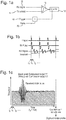
- FIG. 1 an existing receiver architecture for receiving signal waveforms in an impulse radar system using a swept threshold digitization circuit is illustrated in Fig. 1 .
- Fig. 1a shows a comparator 10 that receives the received (RX) signal 12 and a threshold signal 14.
- the comparator is a standard 1-bit comparator. It compares the two inputs and outputs a high signal (high voltage rail) if the received signal 12 is higher than the threshold 14 and a low signal (low voltage rail) otherwise, thus quantising the incoming received signal 12.
- Pulses are transmitted repeatedly at a pulse repetition frequency (PRF). After each pulse is transmitted the threshold signal 14 is changed and the comparison is performed again, thus comparing the received signal 12 against a different threshold (for a high PRF, the received signal is expected to be substantially identical for successive pulses as any movement of reflectors within the range is assumed to be slow compared with the pulse repetition rate, i.e.
- thermometer coded output is turned into a multi-bit sample value of the received signal 10.
- the term "swept-threshold" is used to describe this technique.
- Fig. 1a the counter 16 is triggered by the trigger signal 18 that was also used to generate transmit (TX) pulses.
- a delay 20 provides the overall coarse range gate, i.e. the time at which to start sampling the receive signal 12 (and thus the distance or range at which to look for reflections).
- Fig. 1b illustrates the signals involved, with the trigger signal shown at the top (four individual pulses in the pulse stream are shown, these being generated at the PRF), the transmit pulse that is generated by that trigger signal is shown on the second line, the received signal 12 on the third line (showing two reflections from each transmit pulse) and the step-wise increasing threshold signal 14 on the fourth line.
- the sampling rate should be maximised (i.e. the time between samples minimised), bearing in mind that there is no theoretical benefit to sampling at higher than the Nyquist frequency.
- Traditional (non-swept-threshold) receivers are limited by the speed of the ADCs as the next sample cannot be taken until the ADC has finished processing the previous sample.
- High resolution (i.e. with a high number of bits of digital output) ADCs are typically too slow to sample the RF signal directly and therefore there has traditionally been a trade-off between time resolution and amplitude resolution.
- thermometer coded output is shown in Fig.
- US 2014/292551 describes a sampling and interleaving stage device for use in an analog-digital-converter.
- the sampling and interleaving stage comprises a plurality of clock-driven switches, for each clock-driven switch a first demultiplexer with outputs that output to a storage element for a stored input potential, and an output demultiplexer for receiving an indication about the stored input potential and outputting a corresponding sampling output signal to a respective sampling output.
- FIG. 2 An implementation with multiple parallel counters 16 is shown in Fig. 2 .
- the counters 16 are individually driven by a trigger signal 18 tapped through a series of delay elements 22 constituting an open-loop delay line 20.
- the taps of the delay line (taken from between adjacent delay elements 22) enable the counters 16 to sample and process the quantized signal from the comparator 10, each counter being for a different range point.
- the receive signal 12 is converted into a single-ended rail-to-rail CMOS digital signal by the comparator 10 as follows: the comparator 10 sums the receive signal 12 with the swept threshold signal 14 and compares this summed signal with a fixed input reference the value of which is determined from physical circuit parameters. Depending on whether the summed input is higher or lower than the reference, the output is driven to the high or low rail.
- the comparator applies linear gain which saturates at the supply rails, producing a signal with digital (binary) levels.
- the quantised output signal has finite rise and fall times that vary the pulse width (i.e. times between edges). If the rise times and fall times are too slow (not steep enough) then the width of the pulses can be reduced to the extent that they are insufficient to trigger the downstream logic or sampling latch. This may result in missed counts and erroneous signal digitisation. This is particularly the case with a continuous-in-time signal as rising edges and falling edges can come very close together. The setup and hold requirements of the sampling latch may thus lead to unpredictable results. The impulse sampling that is desired is not achieved because the sampling instant is not well defined.
- the rail-to-rail CMOS signal generates a significant amount of switching noise at high frequencies which is undesirable, as well as drawing significant power (because power is proportional to C ⁇ V dd 2 ⁇ f, where C is the capacitive load, V dd is the supply voltage, i.e. the high level of the signal, and f is the switching frequency).
- each sampler can be re-used during the building up of the range profile.
- a decoder is required for each range point in order to convert the thermometer coded input into a digital value.
- the decoder values may be generated by storing and accumulating the individual bits of the thermometer coded input over multiple pulse transmissions (each bit resulting from a comparison against a threshold value in the swept threshold system).
- the decoder values provide the amplitude resolution.
- Counters are one convenient form of decoder. A counter can be arranged to receive the quantized input and either increase its count or not increase its count based on the quantized input.
- An alternative decoder is a thermometer to binary decoder one form of which may store up the input bits until an output value is required and then process them simultaneously to produce the required output value.
- the counters have all been connected to the received (and quantized) signal in parallel, each with its own sample and hold circuit and each being triggered in sequence so as to sample the receive signal and different times (and hence different range points).
- the large counter circuits provide a capacitive load on the circuit which slows down the rise and fall times of the quantized signal and can, in extreme cases, result in the quantized signal rising too slowly to trigger the counter.
- the capacitive load is significantly reduced and the rise and fall times of the quantizer are not slowed so much.
- the signal can be captured more reliably as there is a much smaller chance of the decoders failing to activate when required.
- the speed of the decoders themselves is not a problem as each decoder does not need to finish its processing before the demultiplexer moves on to the next decoder. It only needs to have commenced processing (although of course it also needs to finish before the next cycle).
- the re-use of the samplers does require a slightly more complex triggering logic and counting logic to control the timing of the samplers and the switching between the different decoders (i.e. controlling the demultiplexers), but the gains in reliability and area saving have been found to justify this complexity.
- the range profile digitization circuit further comprises a controller arranged to generate trigger signals for the plurality of samplers, the trigger signals being generated at regular time intervals.
- the trigger signals could be generated by an open loop delay line such that when a trigger signal is transmitted along the delay line, the delay line taps provide a series of trigger signals in time.
- the controller provides triggers at regular time intervals generated by some form of clock or regulated circuit.
- a delay locked loop (DLL) or a phase locked loop (PLL) provides a good regular timing mechanism, especially when it is driven from a stable oscillator (or other reference source) such as a crystal oscillator.
- a stable oscillator or other reference source
- clocks consume more power than a pure delay line solution, this power consumption is at least partly compensated by the power saving of having a lower parasitic capacitance in the sampling circuitry (as the decoders are better isolated as described above).
- the controller be arranged to generate a continuous stream of trigger signals comprising a plurality of cycles of the plurality of samplers.
- the time interval between the last sampler being triggered and the first sampler being triggered again i.e. the time gap between the end of one sampler cycle and the beginning of the next
- the re-use of the samplers provides a continuous stream of samples, all separated by substantially the same time gap and thus providing regular samples of the range profile.
- the controller comprises a multiphase frequency generator arranged to generate the trigger signals.
- a multiphase frequency generator is beneficial as it can operate at a much lower base clock frequency that draws less power.
- the multiple phases of the frequency generator are used as the trigger signals for the samplers.
- the multiphase frequency generator preferably outputs a number of phases equal to the number of samplers. With the number of phases exactly matched to the number of samplers, the samplers will be cycled continuously as described above.
- a PLL or DLL may be used for the multiphase frequency generator. It will be appreciated that the circuit components such as samplers are typically edge triggered and thus it is the frequency of edge generation of the multiphase frequency generator that determines the actual sampling rate.
- the sampling rate is equal to the base (or external reference) frequency of the multiphase clock generator multiplied by the number of phases that it generates (i.e. the number of samplers).
- an additional clock multiplier may be used to further increase the overall frequency.
- an x8 clock multiplier can be used to further increase the base clock frequency used by the multiphase frequency generator. For example if a PLL is used, it is straight forward to have the PLL multiply the input clock frequency (and output a multiphase clock).
- the range profile digitization circuit further comprises a controller arranged to generate selector inputs for the demultiplexers, the controller being arranged to change the selector input of each demultiplexer every time the corresponding sampler is triggered.
- a decoder e.g. a counter
- a different decoder must be used to measure a different range point.
- the selector input of the associated demultiplexer must be changed so as to direct the next sample to the next decoder. In this way the full set of decoders is used to measure a full set of range points.
- This process is typically used to sample the reflected profile of a single transmit pulse. Once all decoders have been used, the samplers will be disabled until the next transmit pulse is sent (and optionally also a coarse range gate delay has elapsed before measurement starts). The controller will reset the demultiplexer selector inputs so that for the next transmit pulse the new range profile measurements begin again at the first decoder of each sampler so that the same range profile is processed along with the previous corresponding sample (e.g. in the case of a counter, it is counted on top of the previous counts), but with a new threshold level set as described above. This process repeats until all thresholds have been processed. At the end of this process the decoders together provide a time series (i.e. an array) of digital values representing the amplitude of the received signal, i.e. a digitized range profile.
- a time series i.e. an array
- the controller is arranged to generate trigger signals for the plurality of samplers and selector inputs for the demultiplexers; and wherein the controller is arranged to generate trigger signals that cycle through the plurality of samplers a plurality of times; and wherein the controller is arranged to cycle through the demultiplexer selector inputs, changing each demultiplexer's selector input once per cycle of the trigger signals.
- the pulse repetition frequency is at least 10 MHz, preferably at least 20 MHz, optionally at least 50 MHz.
- the base clock frequency of the multiphase frequency generator may be at least 100 MHz, preferably at least 200 MHz.
- at least 5 samplers are provided, more preferably at least 10 samplers.
- each sampler has at least 20 decoders, preferably at least 50 decoders, more preferably at least 100 decoders.
- the range profile digitization circuit comprises 12 samplers, each with 128 decoders, thereby providing 1536 sampling points (range points) in the range profile.
- the sampler may be any form of sampler circuit, but for high speed operations a simple and fast circuit is preferred and therefore preferably the samplers are flip-flops. For example a D-type flip-flop is suitable for this circuit.
- a single quantizer is provided upstream of all of the plurality of samplers. This can be a benefit by ensuring that there is no mismatch between different quantizers.
- a plurality of quantizers is provided, each being associated with one or more of the plurality of samplers. With multiple quantizers, the threshold signal would be distributed to each quantizer. Although the number of quantizers could be lower than the number of samplers, with each quantizer fanning out its output to multiple samplers, it is preferred in such arrangements that one quantizer be provided for each sampler. Advantages of such arrangements will be discussed further below.
- the order of quantization and sampling can be either way round.
- the signal can be quantized immediately prior to sampling the quantized signal.
- the non-quantized signal may be sampled first by the sampler and then the sampled output can be quantized, e.g. by amplifying it to either voltage rail.
- the invention provides a method of range profile digitization according to claim 8.
- the received (RX) signal from the antenna is converted into a single-ended, rail-to-rail CMOS digital signal early in the processing chain such that the signal is quantized before it is fanned out to the multiple samplers and decoders.
- the rise and fall times can be too slow, resulting in narrow pulses that fail to trigger the samplers and also high switching noise at high frequencies.
- a range profile digitization circuit for converting a repeating analog input signal into a time series of digital amplitude values, the converter comprising: a differencer arranged to receive the analog input signal and a threshold input signal and arranged to output a differencer signal being the difference between the analog input signal and the threshold input signal; a plurality of clocked comparators, each clocked comparator being arranged to sample the differencer signal upon receipt of a trigger signal and each clocked comparator being arranged to output and hold an amplified signal; and for each clocked comparator, a decoder which is arranged to decode the quantized signal into a digital value.
- the use of a differencer without a quantizer in the early part of the processing chain means that the signal is not quantized (discretized into one of two binary values) until later in the processing chain.
- the quantization does not take place until the clocked comparators.
- the clocked comparators amplify the signal into one of two discrete binary values (i.e. quantizing it by amplifying the signal until it reaches a rail voltage).
- the regenerative amplification of these clocked comparators has an exponential response and therefore provides a very high gain for resolving small differences between the threshold level and the signal into levels that subsequent circuits can respond to.
- the clocked comparator is a clocked device, it samples, amplifies and holds the amplified value.
- quantization of the signal is avoided prior to sampling of the signal. Only after sampling is the sampled value quantized accordingly.
- This arrangement (as compared with previous designs in which the signal was quantized early in the signal processing) allows the use of regenerative gain in the quantization process as this takes place after sampling (and hence in a clocked part of the circuit rather than in a continuous time part of the circuit). Due to the extremely high gain of the regenerative amplifier, the output will be a binary value as the amplifier rapidly pushes the output to one of the circuit's voltage rails. This output value is passed to the corresponding decoder which, when enabled or triggered, adjusts its value based on that binary value.
- the switching noise is removed or reduced as the regenerative amplification (and switching) only happens immediately after the sampling and prior to the counting operations.
- the noise occurs at predefined points in time and not when the circuit is sampling the input signal. So noise is less likely to interfere during the critical sampling phase.
- the range profile digitization circuit preferably comprises a continuous time amplifier downstream of the differencer, and arranged to amplify the differencer signal.
- the use of a continuous-time (non-regenerative) amplifier early in the signal chain amplifies the incoming signal for use later in the processing chain without pushing the received signal to the rails and without generating switching noise.
- the signal is not made discrete in amplitude (binary value) until it reaches each of the plurality of clocked comparators.
- the output can be analysed by examining its polarity (i.e. amplitude with respect to ground) rather than absolute values. As the polarity can be distinguished much more sensitively, a low gain can be used at this stage, improving the signal to noise ratio without introducing switching noise.
- a limiting gain continuous time amplifier can be used as a buffer to enhance the sensitivity of the quantizers. Limiting gain is possible because we only need the polarity of the signal and helps slew rate requirements. It is not a problem for the signal to clip. i.e. for the output to have some maximum and minimum value, as it is only the polarity of the signal that matters. However it should be noted that the signal does not have to clip, because the regenerative gain will continue the amplification to digital levels later in the processing.
- the system may have a single difference provided before the signal is fanned out to the clocked comparators. This has the advantage of not having to fan out the threshold signal.
- a plurality of differencers may be provided, each with its own threshold input and positioned after the signal has been distributed to the clocked comparators.
- the range profile digitization circuit may comprise a plurality of differencers, one for each clocked comparator and each arranged to receive the analog input signal and the threshold input signal and arranged to output a differencer signal being the difference between the analog input signal and the threshold input signal to its associated clocked comparator.
- the differencer may be an integral part of the clocked comparator circuit.
- This quantizing scheme can be used with the traditional swept threshold architecture with all decoders (counters) provided in parallel and each in association with its own clocked comparator. However, for additional benefits it can also be used with the sampler re-use techniques described above.
- the range profile digitization circuit may comprise, for each clocked comparator, a plurality of decoders and a demultiplexer arranged to receive the amplified output from the clocked comparator and pass it to a selected one of said decoders based on a selector input.
- the range profile digitization circuit may further comprise a controller arranged to generate trigger signals for the plurality of clocked comparators, the trigger signals being generated at regular time intervals.
- the controller may be arranged to generate a continuous stream of trigger signals comprising a plurality of cycles of the plurality of clocked comparators.
- the range profile digitization circuit may further comprise a controller arranged to generate selector inputs for the demultiplexers, the controller being arranged to change the selector input of each demultiplexer every time the corresponding clocked comparator is triggered.
- the controller may be arranged to generate trigger signals for the plurality of clocked comparators and selector inputs for the demultiplexers; and the controller may be arranged to generate trigger signals that cycle through the plurality of clocked comparators a plurality of times; and the controller may be arranged to cycle through the demultiplexer selector inputs, changing each demultiplexer's selector input once per cycle of the trigger signals.
- Each clocked comparator may be formed from a strong-arm latch.
- a strong-arm latch has the advantages of providing the sampling, comparison and regenerative gain / quantizing functions all in one convenient circuit.
- the strong-arm latch operates in there phases, firstly a sampling phase, secondly a comparison / regenerative gain and quantizing phase and thirdly a reset phase.
- the sampling of the receive signal is effected prior to quantizing of it, allowing regenerative gain to be used in the quantization process.
- the strong-arm latch is only one specific circuit design that can be used to achieve the sampling and quantization goals. Other circuits may also be used instead of a strong-arm latch.
- the clocked comparator may be arranged to generate a high or low output based on the polarity of the incoming signal.
- the invention provides a method of range profile digitization for converting a repeating analog input signal into a time series of digital amplitude values, the digitization comprising: taking the difference between the received analog input signal and a threshold input signal; providing the difference signal to a plurality of clocked comparators; each clocked comparator sampling the difference signal upon receipt of a trigger signal and outputting an amplified signal; and for each clocked comparator, decoding the quantized signal to produce a digital value.
- an analog to digital convertor for converting a repeating analog input signal into a time series of digital amplitude values, the converter comprising: a signal quantizer arranged to receive the analog input signal and a threshold input and arranged to output a binary value quantized output signal based on a comparison of the input signal with the threshold signal; a plurality of samplers each arranged to sample and hold its input signal upon receipt of a trigger signal; and for each sampler: a plurality of decoders and a demultiplexer arranged to receive an output from the sampler and pass it to a selected one of said decoders based on a selector input.
- the invention provides an analog to digital converter (ADC) for converting a repeating analog input signal into a time series of digital amplitude values, the converter comprising: a differencer arranged to receive the analog input signal and a threshold input signal and arranged to output a differencer signal being the difference between the analog input signal and the threshold input signal; a plurality of clocked comparators, each clocked comparator being arranged to sample the differencer signal upon receipt of a trigger signal and each clocked comparator being arranged to output and hold an amplified signal; and for each clocked comparator, a decoder which is arranged to decode the quantized signal into a digital value.
- ADC analog to digital converter
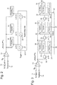
- Fig. 3 shows an impulse radar receiver architecture that operates on the swept threshold principle described and illustrated in relation to Figs. 1a, 1b, 1c and 2 .
- the received signal (including reflections of the transmitted signal) 12 and a threshold signal 14 are provided as inputs to a quantizer 10 that outputs a quantized signal 11 that is either high or low (voltage rails) depending on the comparison of the received signal 12 with the threshold signal 14.
- the quantized signal 11 is still a continuous-time (non-clocked) signal, with a binary value (high or low). This quantized signal 11 is then fanned out to a plurality of samplers 30 which operate in parallel.
- the samplers 30 are triggered by the phase outputs ⁇ n> from a multiphase frequency generator (multiphase clock) 40.
- the outputs ⁇ 0> to ⁇ n-1> are equally spaced from one another and ⁇ n-1> is also equally spaced from the ⁇ 0> of the next F s /n clock cycle.
- the top row of Fig. 4 illustrates the overall effective sampling rate F s with time period t s , although it will be appreciated that this is not a real signal appearing anywhere in the circuit of Fig. 3 .
- each sampler 30 As each sampler 30 is triggered by its corresponding clock phase signal ⁇ 0> to ⁇ n-1>, it samples its continuous-time, binary value input 11 and holds that value for the duration of its clock phase until it is next required to sample the input again.
- the plurality of samplers 30 each receive a different clock phase ⁇ 0> to ⁇ n-1> such that they sample the quantized signal 11 at different times and thus sample different range points in the received signal (different range points in the range profile).
- Each sampler 30 may be a D-type flip-flop.
- each sampler 30 is passed to the input of a demultiplexer 32.
- Each demultiplexer 32 can direct its input to one of several different outputs, depending on the selector input 34 which is provided by controller 50.
- the different outputs of the demultiplexer 32 are each provided to a different counter 36 (being a form of decoder) each of which is arranged to increase its count by one upon receipt of a high signal and not to increase its count when its input is low.
- the controller 50 changes the selector input 34 to select the next counter in the series, i.e. to move the demultiplexer output on to the next counter.
- the demultiplexer 34 attached to the sampler 30 that is driven by clock phase ⁇ 0> initially directs its output to counter 0,0 .
- the next sample from sampler 30 is directed to counter 1,0 and the next sample is directed to counter 2,0 , etc. up to the final counter m,0 .
- the demultiplexer 34 attached to the sampler 30 that is driven by clock phase ⁇ 1> initially directs its output to counter 0,1 .
- each counter 36 represents a different range point in the range profile in the sequence counter 0,0 , counter 0,1 , counter 0,2 , ..., counter 0,n-1 , counter 1,0 , counter 1,1 , counter 1,2 , ..., counter 1,n-1 , ..., counter m-1,0 , counter m-1,1 , counter m-1,2 , ..., counter m-1,n-1 .
- the counting of the various counters 36 is illustrated in the lower half of Fig. 4 , each counter being represented by a pair of lines and a crossing of those lines indicating a change of state (i.e. an increase in counter value).
- the use of the multiphase clock 40 allows multiple adjacent samples to be taken at closely spaced time points without requiring a single fast clock and sampler (i.e. the sampler is distributed).
- the provision of multiple counters 36 per sampler 30 reduces the number of parallel samplers 30 that are required to provide a full range profile (i.e. the samplers are re-used).
- the counters 36 are isolated from the quantizer 10 and thus reduce the capacitive load that is seen by the quantizer 10 and thus producing less impact on the rise and fall times of the quantized signal 11.
- Fig. 5 shows an impulse radar receiver architecture that does not fall within the scope of the claims and that operates on the swept threshold principle described and illustrated in relation to Figs. 1a, 1b, 1c and 2 .
- the received signal (including reflections of the transmitted signal) 12 and a threshold signal 14 are provided as inputs to a difference 60 that outputs the difference between the received signal 12 and the threshold signal 14.
- This difference signal is input into low gain linear amplifier (buffer) 62 that amplifies the signal, but does not quantize it like the quantizer 10 of Figs. 2 and 3 . Instead, the output of amplifier 62 is continuous in time and continuous in value (whereas the output of quantizer 10 of Figs. 2 and 3 was continuous time, binary value). As the signal is not pushed to the voltage rails at this point in the signal processing chain, the switching noise is reduced.
- buffer low gain linear amplifier
- the output 63 of amplifier 62 is fanned out to a plurality of parallel samplers 64 in a similar way to the circuit of Fig. 3 .
- Each sampler 64 also performs the quantization necessary to generate a binary value CMOS signal to trigger the counters 36.
- the quantization takes place after the sampling of the amplifier output 63.
- the quantization does not need to be performed in continuous time, i.e. the signal does not need to be pushed to one of the voltage rails on such a short timescale (which generates high frequency switching noise).
- the amplifier output 63 only needs to be pushed to a voltage rail fast enough to trigger the associated counter 36 before the next sampling event on the associated sampler 64. This can be a much longer time period and allows a slower regenerative amplifier to perform the quantization. Further, this takes place after the sampling and thus any associated switching noise does not affect the sampling, nor does it affect any of the other parallel sampling branches.
- the sampler 64 may comprise separate individual circuits for sampling and then amplifying the sampled value. However, in preferred arrangements a combined circuit is used, most preferably a strong-arm latch circuit is used as this conveniently performs sampling and regenerative amplification in a single efficient circuit.
- the samplers 64 are triggered by the phases ⁇ 0> to ⁇ n-1> from multiphase clock 40 shown in Fig. 4 such that each sampler 64 samples a different time point (and hence range point) in the received signal 12.
- Fig. 5 shows each sampler 64 having only a single counter 36 and is thus an architecture which is analogous to that of Fig. 2 where all range points are sampled by their own individual sampler 64.
- the principles shown in Fig. 3 may also be applied such that each sampler 64 is provided with a demultiplexer 32 and a plurality of counters 36, with the demultiplexers 32 controlled by a controller 50 in the same way as is described above in relation to Fig. 3 .
- the threshold signal 14 is changed over time so as to sweep through a predefined range of voltages. For each threshold voltage level the full range profile is compared and each counter incremented (or not) appropriately. Over the full predefined range of threshold voltages, the counters will gradually build up a value corresponding to the signal level by counting the number of times that the signal 12 was above the threshold 14.
- a differential implementation can also be used. Differential circuits may be preferred for better rejection of coupled noise (such as switching noise).
- a differential signal is conveyed as a positive signal (pos) and an identical but opposite polarity signal (neg), with the signal of interest being the difference between the two, i.e. pos ⁇ neg.
Landscapes
- Engineering & Computer Science (AREA)
- Radar, Positioning & Navigation (AREA)
- Remote Sensing (AREA)
- Computer Networks & Wireless Communication (AREA)
- Physics & Mathematics (AREA)
- General Physics & Mathematics (AREA)
- Theoretical Computer Science (AREA)
- Analogue/Digital Conversion (AREA)
- Structure Of Receivers (AREA)
- Transplanting Machines (AREA)
Claims (11)
- Bereichsprofil-Digitalisierungsschaltung zum Umwandeln eines sich wiederholenden analogen Eingangssignals (12) in eine Zeitreihe digitaler Amplitudenwerte, wobei das sich wiederholende analoge Eingangssignal (12) mehrere Pulse umfasst, wobei die Schaltung umfasst:einen Signalquantisierer (10), eingerichtet, um das analoge Eingangssignal (12) und eine Schwellenwerteingabe (14) zu empfangen, und eingerichtet, um ein quantisiertes Binärwert-Ausgangssignal (11) basierend auf einem Vergleich des Eingangssignals (12) mit dem Schwellenwertsignal (14) auszugeben;eine Vielzahl von Samplern (30), eingerichtet, um das quantisierte Binärwert-Ausgangssignal (11) zu empfangen, und jeweils eingerichtet, um ihr Eingangssignal bei Empfang eines Triggersignals abzutasten und zu halten;für jeden Sampler (30): eine Vielzahl von Decodern (36) und einen Demultiplexer (32), eingerichtet, um eine Ausgabe von dem Sampler (30) zu empfangen und sie basierend auf einer Selektoreingabe (34) an einen ausgewählten der Decoder (36) weiterzuleiten; undeinen Controller (50), eingerichtet, um die Selektoreingaben (34) für die Demultiplexer (32) zu erzeugen, wobei der Controller (50) eingerichtet ist, um die Selektoreingabe (34) von jedem Demultiplexer (32) jedes Mal zu ändern, wenn der entsprechende Sampler (30) getriggert wird; undwobei der Controller (50) so eingerichtet ist, dass, sobald alle Decoder (36) verwendet worden sind, der Controller (50) die Demultiplexer-Selektoreingaben (34) zurücksetzt, sodass für den nächsten Puls eine neue Bereichsprofilmessung wieder an einem ersten Decoder (36) von jedem Sampler (30) beginnt, sodass das gleiche Bereichsprofil zusammen mit der vorherigen entsprechenden Abtastung verarbeitet wird, jedoch mit einem neuen Schwellenwertniveau.
- Bereichsprofil-Digitalisierungsschaltung nach Anspruch 1, wobei der Controller (50) eingerichtet ist, Triggersignale für die Vielzahl von Samplern (30) zu erzeugen, wobei die Triggersignale in regelmäßigen Zeitabständen erzeugt werden.
- Bereichsprofil-Digitalisierungsschaltung nach Anspruch 2, wobei der Controller (50) eingerichtet ist, einen kontinuierlichen Strom von Triggersignalen zu erzeugen, die eine Vielzahl von Zyklen von der Vielzahl von Samplern (30) umfassen.
- Bereichsprofil-Digitalisierungsschaltung nach Anspruch 1, wobei der Controller (50) eingerichtet ist, Triggersignale für die Vielzahl von Samplern (30) und Selektoreingaben (34) für die Demultiplexer (32) zu erzeugen; undwobei der Controller (50) eingerichtet ist, Triggersignale zu erzeugen, die die Vielzahl von Samplern (30) eine Vielzahl von Malen zyklisch durchlaufen; undwobei der Controller (50) eingerichtet ist, um die Selektoreingaben (34) des Demultiplexers (32) zyklisch zu durchlaufen, wobei eine Selektoreingabe (34) jedes Demultiplexers einmal pro Zyklus der Triggersignale geändert wird.
- Bereichsprofil-Digitalisierungsschaltung nach einem vorstehenden Anspruch, wobei die Sampler (30) Flipflops sind.
- Bereichsprofil-Digitalisierungsschaltung nach einem vorstehenden Anspruch, wobei ein einziger Quantisierer (10) allen der Vielzahl von Samplern (30) vorgelagert bereitgestellt ist.
- Bereichsprofil-Digitalisierungsschaltung nach einem der Ansprüche 1 bis 5, wobei eine Vielzahl von Quantisierern (10) bereitgestellt ist, die jeweils einem oder mehreren der Vielzahl von Samplern (30) zugeordnet sind.
- Verfahren zur Bereichsprofil-Digitalisierung zum Umwandeln eines sich wiederholenden analogen Eingangssignals in eine Zeitreihe digitaler Amplitudenwerte, wobei das sich wiederholende analoge Eingangssignal (12) mehrere Pulse umfasst, wobei die Digitalisierung umfasst:Vergleichen des empfangenen analogen Eingangssignals (12) mit einer Schwellenwerteingabe (14) und Quantisieren des analogen Eingangssignals (12) basierend auf dem Vergleich, um ein quantisiertes Binärwert-Ausgangssignal (11) auszugeben;Abtasten des Signals (11) durch eine Vielzahl von Samplern (30), jeweils eingerichtet, um das Signal (11) bei Empfang eines Triggersignals abzutasten und zu halten;für jeden Sampler (30): Leiten der Ausgabe von dem Sampler (30) zu einem ausgewählten einen einer Vielzahl von Decodern (36), die diesem Sampler (30) zugeordnet sind, unter Verwendung eines Demultiplexers (32) und basierend auf einer Selektoreingabe (34) des Demultiplexers (32); undErzeugen der Selektoreingaben (34) für die Demultiplexer (32) und Ändern der Selektoreingabe (34) jedes Demultiplexers (32) jedes Mal, wenn der entsprechende Sampler (30) getriggert wird; undsobald alle Decoder (36) verwendet worden sind, Rücksetzen der Demultiplexer-Selektoreingaben (34), sodass für den nächsten Puls eine neue Bereichsprofilmessung wieder an einem ersten Decoder (36) von jedem Sampler (30) beginnt, sodass das gleiche Bereichsprofil zusammen mit dem vorherigen entsprechenden Abtastwert verarbeitet wird, jedoch mit einem neuen Schwellenwertniveau.
- Verfahren nach Anspruch 8, weiter umfassend:
Erzeugen von Triggersignalen für die Vielzahl von Samplern (30) in regelmäßigen Zeitabständen. - Verfahren nach Anspruch 9, umfassend:
Erzeugen eines kontinuierlichen Stroms von Triggersignalen, die eine Vielzahl von Zyklen der Vielzahl von Samplern (30) umfassen. - Verfahren nach Anspruch 8, umfassend:Erzeugen von Triggersignalen für die Vielzahl von Samplern (30) und Erzeugen von Selektoreingaben (34) für die Demultiplexer (32); undwobei die Triggersignale die Vielzahl von Samplern (30) eine Vielzahl von Malen zyklisch durchlaufen; undzyklisches Durchlaufen der Demultiplexer-Selektoreingaben (34), wobei eine Selektoreingabe (34) jedes Demultiplexers einmal pro Zyklus der Triggersignale geändert wird.
Priority Applications (1)
| Application Number | Priority Date | Filing Date | Title |
|---|---|---|---|
| EP21199188.0A EP3958011A1 (de) | 2017-02-03 | 2018-02-01 | Empfänger |
Applications Claiming Priority (2)
| Application Number | Priority Date | Filing Date | Title |
|---|---|---|---|
| GBGB1701848.2A GB201701848D0 (en) | 2017-02-03 | 2017-02-03 | Reciever |
| PCT/EP2018/052581 WO2018141879A2 (en) | 2017-02-03 | 2018-02-01 | Receiver |
Related Child Applications (2)
| Application Number | Title | Priority Date | Filing Date |
|---|---|---|---|
| EP21199188.0A Division EP3958011A1 (de) | 2017-02-03 | 2018-02-01 | Empfänger |
| EP21199188.0A Division-Into EP3958011A1 (de) | 2017-02-03 | 2018-02-01 | Empfänger |
Publications (2)
| Publication Number | Publication Date |
|---|---|
| EP3577487A2 EP3577487A2 (de) | 2019-12-11 |
| EP3577487B1 true EP3577487B1 (de) | 2021-11-17 |
Family
ID=58462293
Family Applications (2)
| Application Number | Title | Priority Date | Filing Date |
|---|---|---|---|
| EP18704918.4A Active EP3577487B1 (de) | 2017-02-03 | 2018-02-01 | Empfänger |
| EP21199188.0A Pending EP3958011A1 (de) | 2017-02-03 | 2018-02-01 | Empfänger |
Family Applications After (1)
| Application Number | Title | Priority Date | Filing Date |
|---|---|---|---|
| EP21199188.0A Pending EP3958011A1 (de) | 2017-02-03 | 2018-02-01 | Empfänger |
Country Status (6)
| Country | Link |
|---|---|
| US (2) | US11817876B2 (de) |
| EP (2) | EP3577487B1 (de) |
| CN (2) | CN110392841B (de) |
| GB (1) | GB201701848D0 (de) |
| TW (2) | TWI815344B (de) |
| WO (1) | WO2018141879A2 (de) |
Families Citing this family (6)
| Publication number | Priority date | Publication date | Assignee | Title |
|---|---|---|---|---|
| US10531099B2 (en) * | 2016-09-30 | 2020-01-07 | The Mitre Corporation | Systems and methods for distributed quantization of multimodal images |
| CN112821915B (zh) * | 2019-10-31 | 2022-04-26 | 瑞昱半导体股份有限公司 | 数据处理装置与方法 |
| US12584995B2 (en) * | 2021-11-30 | 2026-03-24 | Electronics And Telecommunications Research Institute | Method and apparatus for processing radar signal |
| TWI809918B (zh) * | 2022-06-06 | 2023-07-21 | 國立中山大學 | 時間差異放大器 |
| CN118311503B (zh) * | 2024-06-07 | 2024-09-13 | 深圳大学 | 一种任意可变阈值的单比特宽带雷达系统 |
| CN120046554B (zh) * | 2025-04-07 | 2025-08-12 | 飞腾信息技术有限公司 | 一种逻辑代码质量检查方法、装置、服务器及存储介质 |
Family Cites Families (15)
| Publication number | Priority date | Publication date | Assignee | Title |
|---|---|---|---|---|
| US5257312A (en) * | 1991-05-03 | 1993-10-26 | U.S. Philips Corporation | Time-discrete stereo decoder |
| US6169505B1 (en) * | 1999-02-12 | 2001-01-02 | Agilent Technologies, Inc. | Multi-channel, parallel, matched digital-to-analog conversion method, multi-channel, parallel, matched digital-to-analog converter, and analog drive circuit incorporating same |
| US8013789B2 (en) | 2004-10-06 | 2011-09-06 | Ohio University | Systems and methods for acquisition and tracking of low CNR GPS signals |
| US7656339B2 (en) * | 2008-06-06 | 2010-02-02 | Lsi Corporation | Systems and methods for analog to digital conversion |
| US8157738B2 (en) * | 2009-06-02 | 2012-04-17 | Samplify Systems, Inc. | Ultrasound signal compression |
| EP2457328B1 (de) | 2009-07-24 | 2014-03-26 | Technion Research and Development Foundation, Ltd. | Auf Mehrphasen-Interferometrie basierender photonischer Ultrahochgeschwindigkeits-A/D-Wandler |
| US8792846B2 (en) * | 2010-04-06 | 2014-07-29 | Infineon Technologies Ag | Demodulator and method for demodulating a modulated carrier signal |
| GB201015730D0 (en) | 2010-09-20 | 2010-10-27 | Novelda As | Continuous time cross-correlator |
| US9148649B2 (en) | 2011-10-07 | 2015-09-29 | Massachusetts Institute Of Technology | Methods and apparatus for imaging of occluded objects from scattered light |
| PL222895B1 (pl) | 2013-02-07 | 2016-09-30 | Bumar Elektronika Spółka Akcyjna | Sposób i układ kompresji sygnału radarowego |
| GB201305473D0 (en) * | 2013-03-26 | 2013-05-08 | Ibm | Sampling device with buffer circuit for high-speed adcs |
| US9476962B2 (en) * | 2013-05-02 | 2016-10-25 | The Boeing Company | Device, system and methods using angle of arrival measurements for ADS-B authentication and navigation |
| FR3011701B1 (fr) * | 2013-10-04 | 2017-07-28 | Commissariat Energie Atomique | Dispositif de quantification en temps continu, recepteur de signaux radiofrequence comprenant un tel dispositif et procede de quantification en temps continu |
| US9083347B1 (en) * | 2014-05-16 | 2015-07-14 | Xilinx, Inc. | Built-in integrated circuit debug design |
| GB201514520D0 (en) * | 2015-08-14 | 2015-09-30 | Novelda As | Coupled radar |
-
2017
- 2017-02-03 GB GBGB1701848.2A patent/GB201701848D0/en not_active Ceased
-
2018
- 2018-02-01 CN CN201880010257.1A patent/CN110392841B/zh active Active
- 2018-02-01 US US16/483,166 patent/US11817876B2/en active Active
- 2018-02-01 EP EP18704918.4A patent/EP3577487B1/de active Active
- 2018-02-01 CN CN202410192321.XA patent/CN118033552A/zh active Pending
- 2018-02-01 EP EP21199188.0A patent/EP3958011A1/de active Pending
- 2018-02-01 WO PCT/EP2018/052581 patent/WO2018141879A2/en not_active Ceased
- 2018-02-02 TW TW111108756A patent/TWI815344B/zh active
- 2018-02-02 TW TW107103796A patent/TWI761442B/zh active
-
2023
- 2023-10-13 US US18/379,840 patent/US12191879B2/en active Active
Non-Patent Citations (1)
| Title |
|---|
| None * |
Also Published As
| Publication number | Publication date |
|---|---|
| WO2018141879A3 (en) | 2018-09-20 |
| EP3958011A1 (de) | 2022-02-23 |
| WO2018141879A2 (en) | 2018-08-09 |
| US12191879B2 (en) | 2025-01-07 |
| CN118033552A (zh) | 2024-05-14 |
| EP3577487A2 (de) | 2019-12-11 |
| GB201701848D0 (en) | 2017-03-22 |
| US11817876B2 (en) | 2023-11-14 |
| TWI761442B (zh) | 2022-04-21 |
| CN110392841A (zh) | 2019-10-29 |
| TW202226759A (zh) | 2022-07-01 |
| CN110392841B (zh) | 2024-03-12 |
| US20240039550A1 (en) | 2024-02-01 |
| TW201830865A (zh) | 2018-08-16 |
| US20200007140A1 (en) | 2020-01-02 |
| TWI815344B (zh) | 2023-09-11 |
Similar Documents
| Publication | Publication Date | Title |
|---|---|---|
| US12191879B2 (en) | Receiver | |
| US8970421B1 (en) | High resolution sampling-based time to digital converter | |
| US7515084B1 (en) | Analog to digital converter using asynchronous pulse technology | |
| Zhang et al. | A high linearity TDC with a united-reference fractional counter for LiDAR | |
| US20190253286A1 (en) | Continuous-time sampler circuits | |
| US20220057522A1 (en) | System and method for high dynamic range waveform digitization | |
| Naraghi et al. | A 9b 14µw 0.06 mm 2 ppm adc in 90nm digital cmos | |
| KR20120066307A (ko) | 시간-인터리빙 방식의 펄스신호 복원장치 | |
| CN114157301A (zh) | 双斜坡双沿向下计数模数转换装置及其转换方法 | |
| US9831888B1 (en) | Sort-and delay time-to-digital converter | |
| KR101463062B1 (ko) | 신호 처리 장치 및 방법, 그를 이용한 수신기 그리고 거리 측정 장치 | |
| CN114205545B (zh) | 双斜坡双沿向上计数模数转换装置及其转换方法 | |
| CN119030543B (zh) | 高速流水线时间量化模数转换器 | |
| US11075621B2 (en) | Delay circuit, time to digital converter, and A/D conversion circuit | |
| Narku-Tetteh et al. | A 15b, Sub-10ps resolution, low dead time, wide range two-stage TDC | |
| Hamza et al. | A low-power, 9-Bit, 1.2 ps resolution two-step time-to-digital converter in 65 nm CMOS | |
| US12107596B2 (en) | Successive approximation register based time-to-digital converter using a time difference amplifier | |
| RU2685977C1 (ru) | Атактовый строб-фрейм-дискретизатор субнаносекундных радиоимпульсов | |
| Macpherson et al. | A 2.5 GS/s 3-bit time-based ADC in 90nm CMOS | |
| US10158372B1 (en) | Analog to digital converter | |
| Sachs et al. | Stimulation of UWB-sensors: pulse or maximum sequence? | |
| CN116794962B (zh) | 一种大动态测量范围高分辨率多用途时间数字转换器电路 | |
| US7196651B2 (en) | Analog-to-digital converter (ADC) | |
| Keränen et al. | Algorithmic time-to-digital converter | |
| WO2011142721A1 (en) | System and method of sampling a signal having a plurality of identically shaped pulses |
Legal Events
| Date | Code | Title | Description |
|---|---|---|---|
| STAA | Information on the status of an ep patent application or granted ep patent |
Free format text: STATUS: UNKNOWN |
|
| STAA | Information on the status of an ep patent application or granted ep patent |
Free format text: STATUS: THE INTERNATIONAL PUBLICATION HAS BEEN MADE |
|
| PUAI | Public reference made under article 153(3) epc to a published international application that has entered the european phase |
Free format text: ORIGINAL CODE: 0009012 |
|
| STAA | Information on the status of an ep patent application or granted ep patent |
Free format text: STATUS: REQUEST FOR EXAMINATION WAS MADE |
|
| 17P | Request for examination filed |
Effective date: 20190822 |
|
| AK | Designated contracting states |
Kind code of ref document: A2 Designated state(s): AL AT BE BG CH CY CZ DE DK EE ES FI FR GB GR HR HU IE IS IT LI LT LU LV MC MK MT NL NO PL PT RO RS SE SI SK SM TR |
|
| AX | Request for extension of the european patent |
Extension state: BA ME |
|
| DAV | Request for validation of the european patent (deleted) | ||
| DAX | Request for extension of the european patent (deleted) | ||
| STAA | Information on the status of an ep patent application or granted ep patent |
Free format text: STATUS: EXAMINATION IS IN PROGRESS |
|
| 17Q | First examination report despatched |
Effective date: 20201201 |
|
| GRAP | Despatch of communication of intention to grant a patent |
Free format text: ORIGINAL CODE: EPIDOSNIGR1 |
|
| STAA | Information on the status of an ep patent application or granted ep patent |
Free format text: STATUS: GRANT OF PATENT IS INTENDED |
|
| INTG | Intention to grant announced |
Effective date: 20210204 |
|
| GRAJ | Information related to disapproval of communication of intention to grant by the applicant or resumption of examination proceedings by the epo deleted |
Free format text: ORIGINAL CODE: EPIDOSDIGR1 |
|
| STAA | Information on the status of an ep patent application or granted ep patent |
Free format text: STATUS: EXAMINATION IS IN PROGRESS |
|
| GRAP | Despatch of communication of intention to grant a patent |
Free format text: ORIGINAL CODE: EPIDOSNIGR1 |
|
| STAA | Information on the status of an ep patent application or granted ep patent |
Free format text: STATUS: GRANT OF PATENT IS INTENDED |
|
| INTC | Intention to grant announced (deleted) | ||
| INTG | Intention to grant announced |
Effective date: 20210712 |
|
| GRAS | Grant fee paid |
Free format text: ORIGINAL CODE: EPIDOSNIGR3 |
|
| GRAA | (expected) grant |
Free format text: ORIGINAL CODE: 0009210 |
|
| STAA | Information on the status of an ep patent application or granted ep patent |
Free format text: STATUS: THE PATENT HAS BEEN GRANTED |
|
| AK | Designated contracting states |
Kind code of ref document: B1 Designated state(s): AL AT BE BG CH CY CZ DE DK EE ES FI FR GB GR HR HU IE IS IT LI LT LU LV MC MK MT NL NO PL PT RO RS SE SI SK SM TR |
|
| REG | Reference to a national code |
Ref country code: GB Ref legal event code: FG4D |
|
| REG | Reference to a national code |
Ref country code: IE Ref legal event code: FG4D |
|
| REG | Reference to a national code |
Ref country code: DE Ref legal event code: R096 Ref document number: 602018026772 Country of ref document: DE |
|
| REG | Reference to a national code |
Ref country code: AT Ref legal event code: REF Ref document number: 1448485 Country of ref document: AT Kind code of ref document: T Effective date: 20211215 |
|
| REG | Reference to a national code |
Ref country code: LT Ref legal event code: MG9D |
|
| REG | Reference to a national code |
Ref country code: NL Ref legal event code: MP Effective date: 20211117 |
|
| REG | Reference to a national code |
Ref country code: AT Ref legal event code: MK05 Ref document number: 1448485 Country of ref document: AT Kind code of ref document: T Effective date: 20211117 |
|
| PG25 | Lapsed in a contracting state [announced via postgrant information from national office to epo] |
Ref country code: RS Free format text: LAPSE BECAUSE OF FAILURE TO SUBMIT A TRANSLATION OF THE DESCRIPTION OR TO PAY THE FEE WITHIN THE PRESCRIBED TIME-LIMIT Effective date: 20211117 Ref country code: LT Free format text: LAPSE BECAUSE OF FAILURE TO SUBMIT A TRANSLATION OF THE DESCRIPTION OR TO PAY THE FEE WITHIN THE PRESCRIBED TIME-LIMIT Effective date: 20211117 Ref country code: FI Free format text: LAPSE BECAUSE OF FAILURE TO SUBMIT A TRANSLATION OF THE DESCRIPTION OR TO PAY THE FEE WITHIN THE PRESCRIBED TIME-LIMIT Effective date: 20211117 Ref country code: BG Free format text: LAPSE BECAUSE OF FAILURE TO SUBMIT A TRANSLATION OF THE DESCRIPTION OR TO PAY THE FEE WITHIN THE PRESCRIBED TIME-LIMIT Effective date: 20220217 Ref country code: AT Free format text: LAPSE BECAUSE OF FAILURE TO SUBMIT A TRANSLATION OF THE DESCRIPTION OR TO PAY THE FEE WITHIN THE PRESCRIBED TIME-LIMIT Effective date: 20211117 |
|
| PG25 | Lapsed in a contracting state [announced via postgrant information from national office to epo] |
Ref country code: IS Free format text: LAPSE BECAUSE OF FAILURE TO SUBMIT A TRANSLATION OF THE DESCRIPTION OR TO PAY THE FEE WITHIN THE PRESCRIBED TIME-LIMIT Effective date: 20220317 Ref country code: SE Free format text: LAPSE BECAUSE OF FAILURE TO SUBMIT A TRANSLATION OF THE DESCRIPTION OR TO PAY THE FEE WITHIN THE PRESCRIBED TIME-LIMIT Effective date: 20211117 Ref country code: PT Free format text: LAPSE BECAUSE OF FAILURE TO SUBMIT A TRANSLATION OF THE DESCRIPTION OR TO PAY THE FEE WITHIN THE PRESCRIBED TIME-LIMIT Effective date: 20220317 Ref country code: PL Free format text: LAPSE BECAUSE OF FAILURE TO SUBMIT A TRANSLATION OF THE DESCRIPTION OR TO PAY THE FEE WITHIN THE PRESCRIBED TIME-LIMIT Effective date: 20211117 Ref country code: NO Free format text: LAPSE BECAUSE OF FAILURE TO SUBMIT A TRANSLATION OF THE DESCRIPTION OR TO PAY THE FEE WITHIN THE PRESCRIBED TIME-LIMIT Effective date: 20220217 Ref country code: NL Free format text: LAPSE BECAUSE OF FAILURE TO SUBMIT A TRANSLATION OF THE DESCRIPTION OR TO PAY THE FEE WITHIN THE PRESCRIBED TIME-LIMIT Effective date: 20211117 Ref country code: LV Free format text: LAPSE BECAUSE OF FAILURE TO SUBMIT A TRANSLATION OF THE DESCRIPTION OR TO PAY THE FEE WITHIN THE PRESCRIBED TIME-LIMIT Effective date: 20211117 Ref country code: HR Free format text: LAPSE BECAUSE OF FAILURE TO SUBMIT A TRANSLATION OF THE DESCRIPTION OR TO PAY THE FEE WITHIN THE PRESCRIBED TIME-LIMIT Effective date: 20211117 Ref country code: GR Free format text: LAPSE BECAUSE OF FAILURE TO SUBMIT A TRANSLATION OF THE DESCRIPTION OR TO PAY THE FEE WITHIN THE PRESCRIBED TIME-LIMIT Effective date: 20220218 Ref country code: ES Free format text: LAPSE BECAUSE OF FAILURE TO SUBMIT A TRANSLATION OF THE DESCRIPTION OR TO PAY THE FEE WITHIN THE PRESCRIBED TIME-LIMIT Effective date: 20211117 |
|
| PG25 | Lapsed in a contracting state [announced via postgrant information from national office to epo] |
Ref country code: SM Free format text: LAPSE BECAUSE OF FAILURE TO SUBMIT A TRANSLATION OF THE DESCRIPTION OR TO PAY THE FEE WITHIN THE PRESCRIBED TIME-LIMIT Effective date: 20211117 Ref country code: SK Free format text: LAPSE BECAUSE OF FAILURE TO SUBMIT A TRANSLATION OF THE DESCRIPTION OR TO PAY THE FEE WITHIN THE PRESCRIBED TIME-LIMIT Effective date: 20211117 Ref country code: RO Free format text: LAPSE BECAUSE OF FAILURE TO SUBMIT A TRANSLATION OF THE DESCRIPTION OR TO PAY THE FEE WITHIN THE PRESCRIBED TIME-LIMIT Effective date: 20211117 Ref country code: EE Free format text: LAPSE BECAUSE OF FAILURE TO SUBMIT A TRANSLATION OF THE DESCRIPTION OR TO PAY THE FEE WITHIN THE PRESCRIBED TIME-LIMIT Effective date: 20211117 Ref country code: DK Free format text: LAPSE BECAUSE OF FAILURE TO SUBMIT A TRANSLATION OF THE DESCRIPTION OR TO PAY THE FEE WITHIN THE PRESCRIBED TIME-LIMIT Effective date: 20211117 Ref country code: CZ Free format text: LAPSE BECAUSE OF FAILURE TO SUBMIT A TRANSLATION OF THE DESCRIPTION OR TO PAY THE FEE WITHIN THE PRESCRIBED TIME-LIMIT Effective date: 20211117 |
|
| REG | Reference to a national code |
Ref country code: DE Ref legal event code: R097 Ref document number: 602018026772 Country of ref document: DE |
|
| PLBE | No opposition filed within time limit |
Free format text: ORIGINAL CODE: 0009261 |
|
| STAA | Information on the status of an ep patent application or granted ep patent |
Free format text: STATUS: NO OPPOSITION FILED WITHIN TIME LIMIT |
|
| PG25 | Lapsed in a contracting state [announced via postgrant information from national office to epo] |
Ref country code: MC Free format text: LAPSE BECAUSE OF FAILURE TO SUBMIT A TRANSLATION OF THE DESCRIPTION OR TO PAY THE FEE WITHIN THE PRESCRIBED TIME-LIMIT Effective date: 20211117 |
|
| REG | Reference to a national code |
Ref country code: CH Ref legal event code: PL |
|
| REG | Reference to a national code |
Ref country code: BE Ref legal event code: MM Effective date: 20220228 |
|
| 26N | No opposition filed |
Effective date: 20220818 |
|
| PG25 | Lapsed in a contracting state [announced via postgrant information from national office to epo] |
Ref country code: LU Free format text: LAPSE BECAUSE OF NON-PAYMENT OF DUE FEES Effective date: 20220201 Ref country code: AL Free format text: LAPSE BECAUSE OF FAILURE TO SUBMIT A TRANSLATION OF THE DESCRIPTION OR TO PAY THE FEE WITHIN THE PRESCRIBED TIME-LIMIT Effective date: 20211117 |
|
| PG25 | Lapsed in a contracting state [announced via postgrant information from national office to epo] |
Ref country code: SI Free format text: LAPSE BECAUSE OF FAILURE TO SUBMIT A TRANSLATION OF THE DESCRIPTION OR TO PAY THE FEE WITHIN THE PRESCRIBED TIME-LIMIT Effective date: 20211117 |
|
| PG25 | Lapsed in a contracting state [announced via postgrant information from national office to epo] |
Ref country code: LI Free format text: LAPSE BECAUSE OF NON-PAYMENT OF DUE FEES Effective date: 20220228 Ref country code: IE Free format text: LAPSE BECAUSE OF NON-PAYMENT OF DUE FEES Effective date: 20220201 Ref country code: CH Free format text: LAPSE BECAUSE OF NON-PAYMENT OF DUE FEES Effective date: 20220228 |
|
| PG25 | Lapsed in a contracting state [announced via postgrant information from national office to epo] |
Ref country code: BE Free format text: LAPSE BECAUSE OF NON-PAYMENT OF DUE FEES Effective date: 20220228 |
|
| PG25 | Lapsed in a contracting state [announced via postgrant information from national office to epo] |
Ref country code: IT Free format text: LAPSE BECAUSE OF FAILURE TO SUBMIT A TRANSLATION OF THE DESCRIPTION OR TO PAY THE FEE WITHIN THE PRESCRIBED TIME-LIMIT Effective date: 20211117 |
|
| P01 | Opt-out of the competence of the unified patent court (upc) registered |
Effective date: 20230513 |
|
| PG25 | Lapsed in a contracting state [announced via postgrant information from national office to epo] |
Ref country code: MK Free format text: LAPSE BECAUSE OF FAILURE TO SUBMIT A TRANSLATION OF THE DESCRIPTION OR TO PAY THE FEE WITHIN THE PRESCRIBED TIME-LIMIT Effective date: 20211117 Ref country code: CY Free format text: LAPSE BECAUSE OF FAILURE TO SUBMIT A TRANSLATION OF THE DESCRIPTION OR TO PAY THE FEE WITHIN THE PRESCRIBED TIME-LIMIT Effective date: 20211117 |
|
| PG25 | Lapsed in a contracting state [announced via postgrant information from national office to epo] |
Ref country code: HU Free format text: LAPSE BECAUSE OF FAILURE TO SUBMIT A TRANSLATION OF THE DESCRIPTION OR TO PAY THE FEE WITHIN THE PRESCRIBED TIME-LIMIT; INVALID AB INITIO Effective date: 20180201 |
|
| PG25 | Lapsed in a contracting state [announced via postgrant information from national office to epo] |
Ref country code: TR Free format text: LAPSE BECAUSE OF FAILURE TO SUBMIT A TRANSLATION OF THE DESCRIPTION OR TO PAY THE FEE WITHIN THE PRESCRIBED TIME-LIMIT Effective date: 20211117 |
|
| PG25 | Lapsed in a contracting state [announced via postgrant information from national office to epo] |
Ref country code: MT Free format text: LAPSE BECAUSE OF FAILURE TO SUBMIT A TRANSLATION OF THE DESCRIPTION OR TO PAY THE FEE WITHIN THE PRESCRIBED TIME-LIMIT Effective date: 20211117 |
|
| PGFP | Annual fee paid to national office [announced via postgrant information from national office to epo] |
Ref country code: DE Payment date: 20250220 Year of fee payment: 8 |
|
| PGFP | Annual fee paid to national office [announced via postgrant information from national office to epo] |
Ref country code: FR Payment date: 20250218 Year of fee payment: 8 |
|
| PGFP | Annual fee paid to national office [announced via postgrant information from national office to epo] |
Ref country code: GB Payment date: 20250221 Year of fee payment: 8 |