EP3576165A1 - Procede de fabrication d'une diode electro- luminescente de type gan - Google Patents
Procede de fabrication d'une diode electro- luminescente de type gan Download PDFInfo
- Publication number
- EP3576165A1 EP3576165A1 EP19176768.0A EP19176768A EP3576165A1 EP 3576165 A1 EP3576165 A1 EP 3576165A1 EP 19176768 A EP19176768 A EP 19176768A EP 3576165 A1 EP3576165 A1 EP 3576165A1
- Authority
- EP
- European Patent Office
- Prior art keywords
- layer
- manufacturing
- magnesium
- concentration
- alloy
- Prior art date
- Legal status (The legal status is an assumption and is not a legal conclusion. Google has not performed a legal analysis and makes no representation as to the accuracy of the status listed.)
- Granted
Links
Images


Classifications
-
- H—ELECTRICITY
- H10—SEMICONDUCTOR DEVICES; ELECTRIC SOLID-STATE DEVICES NOT OTHERWISE PROVIDED FOR
- H10H—INORGANIC LIGHT-EMITTING SEMICONDUCTOR DEVICES HAVING POTENTIAL BARRIERS
- H10H20/00—Individual inorganic light-emitting semiconductor devices having potential barriers, e.g. light-emitting diodes [LED]
- H10H20/01—Manufacture or treatment
- H10H20/011—Manufacture or treatment of bodies, e.g. forming semiconductor layers
- H10H20/013—Manufacture or treatment of bodies, e.g. forming semiconductor layers having light-emitting regions comprising only Group III-V materials
- H10H20/0137—Manufacture or treatment of bodies, e.g. forming semiconductor layers having light-emitting regions comprising only Group III-V materials the light-emitting regions comprising nitride materials
-
- C—CHEMISTRY; METALLURGY
- C30—CRYSTAL GROWTH
- C30B—SINGLE-CRYSTAL GROWTH; UNIDIRECTIONAL SOLIDIFICATION OF EUTECTIC MATERIAL OR UNIDIRECTIONAL DEMIXING OF EUTECTOID MATERIAL; REFINING BY ZONE-MELTING OF MATERIAL; PRODUCTION OF A HOMOGENEOUS POLYCRYSTALLINE MATERIAL WITH DEFINED STRUCTURE; SINGLE CRYSTALS OR HOMOGENEOUS POLYCRYSTALLINE MATERIAL WITH DEFINED STRUCTURE; AFTER-TREATMENT OF SINGLE CRYSTALS OR A HOMOGENEOUS POLYCRYSTALLINE MATERIAL WITH DEFINED STRUCTURE; APPARATUS THEREFOR
- C30B25/00—Single-crystal growth by chemical reaction of reactive gases, e.g. chemical vapour-deposition growth
- C30B25/02—Epitaxial-layer growth
-
- C—CHEMISTRY; METALLURGY
- C30—CRYSTAL GROWTH
- C30B—SINGLE-CRYSTAL GROWTH; UNIDIRECTIONAL SOLIDIFICATION OF EUTECTIC MATERIAL OR UNIDIRECTIONAL DEMIXING OF EUTECTOID MATERIAL; REFINING BY ZONE-MELTING OF MATERIAL; PRODUCTION OF A HOMOGENEOUS POLYCRYSTALLINE MATERIAL WITH DEFINED STRUCTURE; SINGLE CRYSTALS OR HOMOGENEOUS POLYCRYSTALLINE MATERIAL WITH DEFINED STRUCTURE; AFTER-TREATMENT OF SINGLE CRYSTALS OR A HOMOGENEOUS POLYCRYSTALLINE MATERIAL WITH DEFINED STRUCTURE; APPARATUS THEREFOR
- C30B29/00—Single crystals or homogeneous polycrystalline material with defined structure characterised by the material or by their shape
- C30B29/10—Inorganic compounds or compositions
- C30B29/40—AIIIBV compounds wherein A is B, Al, Ga, In or Tl and B is N, P, As, Sb or Bi
- C30B29/403—AIII-nitrides
- C30B29/406—Gallium nitride
-
- H—ELECTRICITY
- H10—SEMICONDUCTOR DEVICES; ELECTRIC SOLID-STATE DEVICES NOT OTHERWISE PROVIDED FOR
- H10H—INORGANIC LIGHT-EMITTING SEMICONDUCTOR DEVICES HAVING POTENTIAL BARRIERS
- H10H20/00—Individual inorganic light-emitting semiconductor devices having potential barriers, e.g. light-emitting diodes [LED]
- H10H20/01—Manufacture or treatment
-
- H—ELECTRICITY
- H10—SEMICONDUCTOR DEVICES; ELECTRIC SOLID-STATE DEVICES NOT OTHERWISE PROVIDED FOR
- H10H—INORGANIC LIGHT-EMITTING SEMICONDUCTOR DEVICES HAVING POTENTIAL BARRIERS
- H10H20/00—Individual inorganic light-emitting semiconductor devices having potential barriers, e.g. light-emitting diodes [LED]
- H10H20/01—Manufacture or treatment
- H10H20/011—Manufacture or treatment of bodies, e.g. forming semiconductor layers
- H10H20/013—Manufacture or treatment of bodies, e.g. forming semiconductor layers having light-emitting regions comprising only Group III-V materials
- H10H20/0133—Manufacture or treatment of bodies, e.g. forming semiconductor layers having light-emitting regions comprising only Group III-V materials with a substrate not being Group III-V materials
- H10H20/01335—Manufacture or treatment of bodies, e.g. forming semiconductor layers having light-emitting regions comprising only Group III-V materials with a substrate not being Group III-V materials the light-emitting regions comprising nitride materials
-
- H—ELECTRICITY
- H10—SEMICONDUCTOR DEVICES; ELECTRIC SOLID-STATE DEVICES NOT OTHERWISE PROVIDED FOR
- H10H—INORGANIC LIGHT-EMITTING SEMICONDUCTOR DEVICES HAVING POTENTIAL BARRIERS
- H10H20/00—Individual inorganic light-emitting semiconductor devices having potential barriers, e.g. light-emitting diodes [LED]
- H10H20/80—Constructional details
- H10H20/81—Bodies
-
- H—ELECTRICITY
- H10—SEMICONDUCTOR DEVICES; ELECTRIC SOLID-STATE DEVICES NOT OTHERWISE PROVIDED FOR
- H10H—INORGANIC LIGHT-EMITTING SEMICONDUCTOR DEVICES HAVING POTENTIAL BARRIERS
- H10H20/00—Individual inorganic light-emitting semiconductor devices having potential barriers, e.g. light-emitting diodes [LED]
- H10H20/80—Constructional details
- H10H20/81—Bodies
- H10H20/811—Bodies having quantum effect structures or superlattices, e.g. tunnel junctions
-
- H—ELECTRICITY
- H10—SEMICONDUCTOR DEVICES; ELECTRIC SOLID-STATE DEVICES NOT OTHERWISE PROVIDED FOR
- H10H—INORGANIC LIGHT-EMITTING SEMICONDUCTOR DEVICES HAVING POTENTIAL BARRIERS
- H10H20/00—Individual inorganic light-emitting semiconductor devices having potential barriers, e.g. light-emitting diodes [LED]
- H10H20/80—Constructional details
- H10H20/81—Bodies
- H10H20/811—Bodies having quantum effect structures or superlattices, e.g. tunnel junctions
- H10H20/812—Bodies having quantum effect structures or superlattices, e.g. tunnel junctions within the light-emitting regions, e.g. having quantum confinement structures
-
- H—ELECTRICITY
- H10—SEMICONDUCTOR DEVICES; ELECTRIC SOLID-STATE DEVICES NOT OTHERWISE PROVIDED FOR
- H10H—INORGANIC LIGHT-EMITTING SEMICONDUCTOR DEVICES HAVING POTENTIAL BARRIERS
- H10H20/00—Individual inorganic light-emitting semiconductor devices having potential barriers, e.g. light-emitting diodes [LED]
- H10H20/80—Constructional details
- H10H20/81—Bodies
- H10H20/8215—Bodies characterised by crystalline imperfections, e.g. dislocations; characterised by the distribution of dopants, e.g. delta-doping
-
- H—ELECTRICITY
- H10—SEMICONDUCTOR DEVICES; ELECTRIC SOLID-STATE DEVICES NOT OTHERWISE PROVIDED FOR
- H10H—INORGANIC LIGHT-EMITTING SEMICONDUCTOR DEVICES HAVING POTENTIAL BARRIERS
- H10H20/00—Individual inorganic light-emitting semiconductor devices having potential barriers, e.g. light-emitting diodes [LED]
- H10H20/80—Constructional details
- H10H20/81—Bodies
- H10H20/822—Materials of the light-emitting regions
- H10H20/824—Materials of the light-emitting regions comprising only Group III-V materials, e.g. GaP
-
- H—ELECTRICITY
- H10—SEMICONDUCTOR DEVICES; ELECTRIC SOLID-STATE DEVICES NOT OTHERWISE PROVIDED FOR
- H10H—INORGANIC LIGHT-EMITTING SEMICONDUCTOR DEVICES HAVING POTENTIAL BARRIERS
- H10H20/00—Individual inorganic light-emitting semiconductor devices having potential barriers, e.g. light-emitting diodes [LED]
- H10H20/80—Constructional details
- H10H20/81—Bodies
- H10H20/822—Materials of the light-emitting regions
- H10H20/824—Materials of the light-emitting regions comprising only Group III-V materials, e.g. GaP
- H10H20/825—Materials of the light-emitting regions comprising only Group III-V materials, e.g. GaP containing nitrogen, e.g. GaN
-
- H—ELECTRICITY
- H10—SEMICONDUCTOR DEVICES; ELECTRIC SOLID-STATE DEVICES NOT OTHERWISE PROVIDED FOR
- H10P—GENERIC PROCESSES OR APPARATUS FOR THE MANUFACTURE OR TREATMENT OF DEVICES COVERED BY CLASS H10
- H10P14/00—Formation of materials, e.g. in the shape of layers or pillars
- H10P14/20—Formation of materials, e.g. in the shape of layers or pillars of semiconductor materials
- H10P14/24—Formation of materials, e.g. in the shape of layers or pillars of semiconductor materials using chemical vapour deposition [CVD]
-
- H—ELECTRICITY
- H10—SEMICONDUCTOR DEVICES; ELECTRIC SOLID-STATE DEVICES NOT OTHERWISE PROVIDED FOR
- H10P—GENERIC PROCESSES OR APPARATUS FOR THE MANUFACTURE OR TREATMENT OF DEVICES COVERED BY CLASS H10
- H10P14/00—Formation of materials, e.g. in the shape of layers or pillars
- H10P14/20—Formation of materials, e.g. in the shape of layers or pillars of semiconductor materials
- H10P14/32—Formation of materials, e.g. in the shape of layers or pillars of semiconductor materials characterised by intermediate layers between substrates and deposited layers
- H10P14/3202—Materials thereof
- H10P14/3214—Materials thereof being Group IIIA-VA semiconductors
- H10P14/3216—Nitrides
-
- H—ELECTRICITY
- H10—SEMICONDUCTOR DEVICES; ELECTRIC SOLID-STATE DEVICES NOT OTHERWISE PROVIDED FOR
- H10P—GENERIC PROCESSES OR APPARATUS FOR THE MANUFACTURE OR TREATMENT OF DEVICES COVERED BY CLASS H10
- H10P14/00—Formation of materials, e.g. in the shape of layers or pillars
- H10P14/20—Formation of materials, e.g. in the shape of layers or pillars of semiconductor materials
- H10P14/32—Formation of materials, e.g. in the shape of layers or pillars of semiconductor materials characterised by intermediate layers between substrates and deposited layers
- H10P14/3242—Structure
- H10P14/3244—Layer structure
- H10P14/3251—Layer structure consisting of three or more layers
- H10P14/3252—Alternating layers, e.g. superlattice
-
- H—ELECTRICITY
- H10—SEMICONDUCTOR DEVICES; ELECTRIC SOLID-STATE DEVICES NOT OTHERWISE PROVIDED FOR
- H10P—GENERIC PROCESSES OR APPARATUS FOR THE MANUFACTURE OR TREATMENT OF DEVICES COVERED BY CLASS H10
- H10P14/00—Formation of materials, e.g. in the shape of layers or pillars
- H10P14/20—Formation of materials, e.g. in the shape of layers or pillars of semiconductor materials
- H10P14/32—Formation of materials, e.g. in the shape of layers or pillars of semiconductor materials characterised by intermediate layers between substrates and deposited layers
- H10P14/3242—Structure
- H10P14/3244—Layer structure
- H10P14/3254—Graded layers
-
- H—ELECTRICITY
- H10—SEMICONDUCTOR DEVICES; ELECTRIC SOLID-STATE DEVICES NOT OTHERWISE PROVIDED FOR
- H10P—GENERIC PROCESSES OR APPARATUS FOR THE MANUFACTURE OR TREATMENT OF DEVICES COVERED BY CLASS H10
- H10P14/00—Formation of materials, e.g. in the shape of layers or pillars
- H10P14/20—Formation of materials, e.g. in the shape of layers or pillars of semiconductor materials
- H10P14/34—Deposited materials, e.g. layers
- H10P14/3402—Deposited materials, e.g. layers characterised by the chemical composition
- H10P14/3414—Deposited materials, e.g. layers characterised by the chemical composition being group IIIA-VIA materials
- H10P14/3416—Nitrides
-
- H—ELECTRICITY
- H10—SEMICONDUCTOR DEVICES; ELECTRIC SOLID-STATE DEVICES NOT OTHERWISE PROVIDED FOR
- H10P—GENERIC PROCESSES OR APPARATUS FOR THE MANUFACTURE OR TREATMENT OF DEVICES COVERED BY CLASS H10
- H10P14/00—Formation of materials, e.g. in the shape of layers or pillars
- H10P14/20—Formation of materials, e.g. in the shape of layers or pillars of semiconductor materials
- H10P14/34—Deposited materials, e.g. layers
- H10P14/3438—Doping during depositing
- H10P14/3441—Conductivity type
- H10P14/3444—P-type
Definitions
- the invention relates to GaN-type light-emitting diodes and in particular to methods of manufacturing such light-emitting diodes.
- the manufacture of light-emitting diodes including GaN alloy layers assumes the doping of some of these layers with P-type dopants. P-type doping is relatively difficult to achieve because the acceptor levels are deep. Thus, the proportion of ionization of the P-type dopant at room temperature remains relatively low. Due to its relatively low ionization energy, magnesium is frequently used as the P-type dopant for the GaN alloy layers. The solubility of magnesium in GaN alloys, however, remains low. Thus, during a superposition of a P-doped GaN alloy layer and a GaN layer without intentional doping of magnesium, Magnesium is found in this last layer of GaN, called NID. The decrease in the concentration of magnesium in the GaN NID alloy layer since its interface with the pGaN alloy layer is relatively slow, a significant Magnesium concentration can be observed over a thickness of about 100 nm of the layer of alloy GaN nest.
- GaN-type light-emitting diodes For the production of GaN-type light-emitting diodes, a stack of layers is produced, the last functional layer deposited during the manufacturing process generally being a layer of pGaN alloy using magnesium as dopant. A contact electrode must then be formed on the upper face of this stack. For this structure, the decrease in magnesium concentration is not a problem.
- a method described in the publication ' ⁇ LEDs with tunnel junction by MBE and MOCVD + MBE' published in 2015 in Applied Physics Letters, 107, 051107 , uses a nGaN alloy layer on the pGaN alloy layer to form a tunnel junction.
- the nGaN and pGaN alloy layers are formed by MOCVD epitaxy steps, the nGaN alloy layer has a significant Magnesium concentration. The tunnel junction then becomes inoperative.
- the invention aims to solve one or more of these disadvantages.
- the invention thus relates to a method of manufacturing a light-emitting diode, as defined in the appended claims.
- the invention also relates to the variants of the dependent claims.
- Those skilled in the art will understand that each of the features of the variants of the description or the dependent claims may be independently combined with the characteristics of an independent claim, without constituting an intermediate generalization.
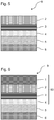
- the figure 1 is a schematic cross sectional view of a multilayer structure 9, made by a manufacturing method according to the invention.
- the multilayer structure 9 comprises an electroluminescent diode 90, formed on a buffer layer 5.
- the buffer layer 5 is fixed on a substrate 6.
- the association of layers 1 and 2 forms a tunnel junction.
- An appropriate combination of layer 1 and 2 materials to form a tunnel junction is known per se to those skilled in the art.
- the upper face of the layer 1 is intended to form a contact interface for an electrode not shown.
- the light-emitting diode 9 is of GaN type, with emission in the visible or ultraviolet spectrum.
- the substrate 6 has a structure known per se.
- the substrate 6 may be an insulator or semiconductor intrinsic or doped silicon type, or SiC sapphire or even AlN or GaN.
- the substrate 6 may typically have a thickness of the order of 350 microns to 1.5 mm and a diameter of the order of 10 mm to 300 mm.
- a non-illustrated adaptation layer may be interposed between the substrate 6 and the buffer layer 5.
- the buffer layer 5 is for example unintentionally doped GaN.
- the AlGaN layer 4 has an N doping, with for example a silicon or germanium concentration typically between 1 * 10 17 cm -3 and 1 * 10 19 cm -3 .
- the layer 3 of multiple quantum wells has a structure known per se, with for example several alternations of a stack of GaN and InGaN layers, or AlGaN / GaN or even AlxGa (1-x) N / Al y Ga layers. (1-y) N where x ⁇ y.
- the P-doped AlGaN layer 2 may for example have, in a manner known per se, a thickness typically between 50 nm and 400 nm and a chemical concentration of magnesium typically between 1 * 18 cm -3 and 1 * 10 20 cm -3 .
- the doping doped P is here obtained by magnesium ionization introduced into the AlGaN of the layer 2.
- the layer 2 can also be made of any other GaN alloy.
- the N-doped AlGaN layer 1 may, for example, have, in a manner known per se, a thickness typically between 20 and 200 nm and a dopant concentration N that is typically between 1 * 10 18 cm -3 and 1 * 10 20 cm -3 .
- the concentration of the dopant may be greater near the junction, and less important towards the surface.
- the layer 2 may also be made of any other GaN alloy, for example an InGaN alloy.
- FIGS. 2 to 6 are schematic sectional views illustrating different steps of a manufacturing method according to an embodiment of the invention.
- a multilayer structure 9 in formation provided with a substrate 6 surmounted by a buffer layer 5, an AlGaN layer 4 and a layer 3 of multiple quantum wells, as described above and obtainable by methods known per se.
- a layer of pAlGaN 20 is deposited according to parameters known per se.
- a gaseous atmosphere is created in the chamber, with a mixture including Gallium precursors (for example TMGa), aluminum (for example TMAI), magnesium (for example Cp 2 Mg), ammonia, hydrogen and nitrogen.
- the partial pressure of ammonia in the mixture is typically between 2000 and 8000 Pa for this step.
- the concentration of a gas in the atmosphere inside the chamber may be expressed as the ratio of the partial pressure of this gas to the total pressure in the chamber.
- the magnesium partial pressure is set at a level which makes it possible to obtain the desired concentration of magnesium for layer 2.
- a mean chemical concentration of magnesium at least equal to 1 * 10 19 cm -3 , or even to less than 1 * 10 20 cm -3 in the layer 2.
- the temperature in the chamber for effecting the epitaxial growth of the layer 20 is, for example, 1000 ° C.
- the deposition of the pAlGaN layer 20 may advantageously be made with a thickness of between 50 and 400 nm.
- the figure 4 illustrates another step of the manufacturing method according to the embodiment.
- the gaseous atmosphere is modified in the chamber by eliminating the magnesium supply from the atmosphere of the chamber.
- the chamber is thus maintained in a gaseous atmosphere of epitaxial growth with a mixture including gallium, ammonia, dihydrogen and nitrogen.
- a layer 21 of GaN is deposited on the pAlGaN layer 20, with conditions of formation of a GaN layer of unintentionally doped type.
- the partial pressure of ammonia in the mixture for the deposition of the layer 21 is typically between 4000 and 15000 Pa for this step.
- the temperature in the chamber for effecting the epitaxial growth of the layer 21 is, for example, 1050 ° C.
- the deposition of the GaN layer 21 can advantageously be carried out over a thickness of between 50 and 200 nm. Due to the memory effect of the magnesium used during the deposition of the layer 20, the layer 21 also includes magnesium. The magnesium concentration decreases in layer 21 as one moves away from its interface with layer 20.
- the multilayer structure 9 was maintained in the epitaxial growth chamber.
- the atmosphere is then placed inside the chamber under conditions of removal of the layer 21 and / or the upper part of the layer 20.
- the atmosphere inside the enclosure for this removal step here has a Cg1 concentration of ammonia, at most equal to one third of the ammonia Cd1 concentration of the atmosphere during the deposition of the layer. 20.
- the Cg1 concentration is at most equal to 10% of the Cd1 concentration.
- the withdrawal step here includes the withdrawal of the entire layer 21. The shrinkage is performed by a desorption mechanism of the layer 21.
- the ammonia Cg1 concentration in the atmosphere during this removal step is non-zero, in order to stabilize the etching / removal process.
- the concentration of ammonia Cg1 in the atmosphere inside the enclosure for this removal step may for example be at least 4% of the Cd1 concentration, and may for example be equal to 5% of the Cd1 concentration. .
- the removal of the upper part of the precursor layer is advantageously carried out over a thickness of at least 20 nm, in order to favor the decaying front of the magnesium concentration.
- the atmosphere used to carry out this removal step also includes dihydrogen and this removal is carried out at a temperature of 1050 ° C. With such withdrawal conditions, an etching rate of 2 ⁇ m / h was obtained for layer 21 with a Cg1 ammonia concentration of 5% of the Cd1 concentration or an ammonia partial pressure of between 200 and 300 Pa.
- the atmosphere inside the chamber for this removal step here has a zero ammonia concentration.
- the removal step here comprises the removal of the entire layer 21.
- the shrinkage is achieved by a desorption mechanism of the layer 21.
- the removal of the upper part of the precursor layer is advantageously carried out over a thickness of at least 20 nm, in order to favor the decaying front of the magnesium concentration.
- the atmosphere used to carry out this removal step comprises dihydrogen and this removal is carried out at a temperature of 1050 ° C. With such withdrawal conditions, an etching rate of 12 ⁇ m / h was obtained for layer 21.
- the layer 20 is either used as a stop layer after the etching of the layer 21 (the layer 20 is AlGaN while the layer 21 is GaN), or undergoes additional etching while maintaining the withdrawal conditions.
- Layer 2 is then obtained from layer 20, as illustrated in FIG. figure 5 .
- the layer 21 is GaN while the layer 20 is AlGaN
- this layer 20 naturally forms a barrier layer for the etching conditions of the layer 21 in the epitaxy chamber.
- the use of the layer 20 as a stop layer makes it possible to limit the dispersions of the manufacturing process, while guaranteeing good control of the etching step of the layer 21.
- the layer 20 may also be GaN, without forming a barrier layer.
- a layer 1 was deposited on layer 2.
- epitaxial deposition of layer 1 of N-doped AlGaN on layer 2 was carried out. the object of a step of mechanopolishing after its deposit.
- magnesium may be passivated by hydrogen from ammonia.
- the presence of layer 1 can make hydrogen removal complicated.
- a depassivation annealing can be performed after the removal of the sacrificial layer 21.
- Nitrogen is then used as a carrier gas, for example with hydrazine (or any other molecule that does not generate hydrogen) as a precursor to nitrogen, to avoid the incorporation of hydrogen, and the passivation of magnesium.
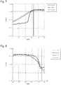
- the figure 7 is a comparative diagram of the concentration M in magnesium as a function of the position D in the depth of a multilayer structure, and according to its manufacturing process.
- a zero depth D corresponds to the upper face of layer 1 of structure 9.
- a depth of 0.27 ⁇ m corresponds to the interface between layer 1 and layer 2.
- the dashed line curve corresponds to a structure made according to a method of the state of the art, in which a layer of GaN 1 is deposited by epitaxy immediately after the epitaxial deposition of a layer of pGaN 2.
- the dashed curve corresponds to a structure produced by a method of the state of the art, in which a 5-minute annealing is carried out between the deposition of a layer of pGaN 2 and the deposition of a layer of GaN 1, by removing the gallium (TMGa) of the atmosphere of the enclosure during this annealing.
- the curve in continuous line corresponds to a structure 1 obtained with a manufacturing method according to the embodiment of the invention.
- a thickness of the GaN 1 layer of at least 100 nm is necessary for a method according to the state of the art, for reducing the magnesium concentration by one decade compared to its interface with the layer 2. Even with a method according to the state of the art implementing an annealing step, such a thickness of the GaN 1 layer is necessary to reduce the magnesium concentration of a decade by report at the interface with layer 2.
- the magnesium concentration decreases by a decade with a thickness of GaN 1 layer of about 30 nm for a structure 9 made according to the embodiment of the invention.
- the manufacturing method according to the invention thus makes it possible to increase the decreasing slope of the magnesium concentration in the layer of AlGaN 1 formed on the layer 2.
- the slope of decrease of the concentration of magnesium in the layer of AlGaN 1 formed on the layer 2 is particularly steep.
- the formation of a conductive electrode on the AlGaN 1 layer is facilitated, without altering the properties of the AlGaN 2 layer.
- Such a result is moreover obtained without polluting the interface between the layers 1 and 2, because of the maintenance of the structure 9 in the epitaxial chamber.
- the manufacturing process is also relatively fast, because of the maintenance of the structure 9 in the epitaxy chamber during these different steps of the process.
- the step of removing the layer 21 is here advantageously carried out by maintaining a certain concentration of ammonia in the atmosphere of the chamber.
- a withdrawal makes it possible both to obtain a sufficiently high withdrawal rate to implement an industrial process quickly, and sufficiently low to control the withdrawal process.
- a such removal can be carried out under the same temperature conditions as the deposition of the layer 20, which avoids the need for prior cooling of the structure.
- the step of forming layer 20 (precursor of layer 2) can be carried out so that the concentration of magnesium in the bottom of this layer 20 is very abrupt. . With such a steep front, one can use a layer 2 even less thick.
- the step of depositing the precursor layer 20 in pAlGaN detailed with reference to the figure 3 can be implemented as follows.
- the surface of the layer is previously saturated with magnesium, before the epitaxial growth conditions of the pAlGaN precursor layer are established.
- the addition of the magnesium precursor in the chamber to achieve the magnesium saturation of the surface may advantageously be carried out for a period of at least 10 seconds.
- the deposition of the pAlGaN layer 20 is initiated with epitaxial growth conditions as described with reference to figure 3 .
- the saturation is made by sending the precursor of magnesium without sending the precursor of gallium, or with very little of the precursor of gallium.
- the figure 8 illustrates a comparative diagram of the magnesium concentration in the thickness of the pAlGaN 2 layer as a function of the duration of maintenance of the magnesium atmosphere, prior to epitaxial deposition of the pAlGaN layer.
- the vertical line corresponds to the bottom of the layer 2.
- the dashed line curve corresponds to a production method devoid of maintaining the atmosphere of the epitaxial chamber with magnesium before epitaxial deposition of the pAlGaN layer.
- the dashed line corresponds to a manufacturing process in which the atmosphere of the epitaxy chamber is maintained with magnesium for a period of 30 seconds before the deposition. by epitaxy of the pAlGaN layer.
- the dash-dot curve corresponds to a manufacturing process in which the atmosphere of the epitaxy chamber is maintained with magnesium for a period of 90 seconds before epitaxial deposition of the pAlGaN layer.
- the dashed curve corresponds to a manufacturing process in which the atmosphere of the epitaxial chamber is maintained with magnesium for a period of 120 seconds before epitaxial deposition of the pAlGaN layer. It can be seen that the longer the atmosphere is maintained with magnesium before entering the epitaxial conditions, the steeper the Magnesium concentration front at the bottom of layer 2 is.
- the invention proves particularly advantageous for a structure 9 intended to form light emitting diode pixel matrices because the method of manufacturing these components imposes constraints on the choice of metallization for the contacts, and therefore the tunnel junction allows the use of different metals while keeping a good contact.
Landscapes
- Chemical & Material Sciences (AREA)
- Engineering & Computer Science (AREA)
- Crystallography & Structural Chemistry (AREA)
- Materials Engineering (AREA)
- Metallurgy (AREA)
- Organic Chemistry (AREA)
- Inorganic Chemistry (AREA)
- Chemical Kinetics & Catalysis (AREA)
- General Chemical & Material Sciences (AREA)
- Led Devices (AREA)
- Chemical Vapour Deposition (AREA)
- Recrystallisation Techniques (AREA)
Abstract
Description
- L'invention concerne les diodes électroluminescentes de type GaN et en particulier les procédés de fabrication de telles diodes électroluminescentes.
- La fabrication de diodes électroluminescentes incluant des couches d'alliage de GaN suppose le dopage de certaines de ces couches avec des dopants de type P. Un dopage de type P est relativement délicat à réaliser car les niveaux d'accepteur sont profonds. Ainsi, la proportion d'ionisation du dopant de type P à température ambiante reste relativement basse. Du fait de son énergie d'ionisation relativement faible, on utilise fréquemment du Magnésium comme dopant de type P pour les couches d'alliage de GaN. La solubilité du Magnésium dans des alliages de GaN reste cependant faible. Ainsi, lors d'une superposition d'une couche d'alliage de GaN dopée P et d'une couche de GaN sans dopage intentionnel de magnésium, on retrouve du Magnésium dans cette dernière couche de GaN, dite NID. La décroissance de la concentration de magnésium dans la couche d'alliage de GaN NID depuis son interface avec la couche d'alliage pGaN est relativement lente, une concentration de Magnésium non négligeable pouvant être constatée sur une épaisseur de l'ordre de 100nm de la couche d'alliage GaN nid.
- Pour la fabrication de diodes électroluminescentes de type GaN, on réalise un empilement de couches, la dernière couche fonctionnelle déposée lors du procédé de fabrication étant généralement une couche d'alliage pGaN utilisant le Magnésium comme dopant. Une électrode de contact doit alors être formée sur la face supérieure de cet empilement. Pour cette structure, la décroissance de la concentration de magnésium n'est pas gênante. Cependant, en vue d'améliorer la résistance de contact sur la face supérieure de l'empilement, un procédé décrit dans la publication 'µLEDs with tunnel junction by MBE and MOCVD+MBE', publié en 2015 dans Applied Physics Letters, 107, 051107, utilise une couche d'alliage nGaN sur la couche d'alliage pGaN pour former une jonction tunnel.
- Lorsque les couches d'alliage nGaN et pGaN sont formées par des étapes d'épitaxie par MOCVD, la couche d'alliage nGaN présente une concentration non négligeable en Magnésium. La jonction tunnel devient alors inopérante.
- L'invention vise à résoudre un ou plusieurs de ces inconvénients. L'invention porte ainsi sur un procédé de fabrication d'une diode électroluminescente, tel que défini dans les revendications annexées.
- L'invention porte également sur les variantes des revendications dépendantes. L'homme du métier comprendra que chacune des caractéristiques des variantes de la description ou des revendications dépendantes peut être combinée indépendamment aux caractéristiques d'une revendication indépendante, sans pour autant constituer une généralisation intermédiaire.
- D'autres caractéristiques et avantages de l'invention ressortiront clairement de la description qui en est faite ci-après, à titre indicatif et nullement limitatif, en référence aux dessins annexés, dans lesquels :
- la
figure 1 est une vue en coupe schématique d'une structure multicouche réalisée par un procédé de fabrication selon l'invention ; - les
figures 2 à 6 sont des vues en coupe schématiques de différentes étapes d'un procédé de fabrication selon un mode de réalisation de l'invention ; - la
figure 7 est un diagramme comparatif de la concentration en Magnésium dans l'épaisseur d'une structure multicouche, en fonction de son procédé de fabrication ; - la
figure 8 est un diagramme comparatif de la concentration en Magnésium dans l'épaisseur d'une structure multicouche, en fonction de variantes de procédés de fabrication selon un autre aspect de l'invention. - La
figure 1 est une vue en coupe transversale schématique d'une structure multicouche 9, réalisée par un procédé de fabrication selon l'invention. La structure multicouche 9 comprend une diode électroluminescente 90, formée sur une couche tampon 5. La couche tampon 5 est fixée sur un substrat 6. - La diode électroluminescente 90 inclut ici :
- une couche 4 en AlGaN dopé N, formée sur la couche tampon 5 ;
- une couche 3 de puits quantiques multiples, formée sur la couche 4 ;
- une couche 2 en AlGaN dopé P, formée sur la couche 3 ;
- une couche 1 en AlGaN dopé N, formée sur la couche 2.
- L'association des couches 1 et 2 forme une jonction tunnel. Une association appropriée de matériaux des couches 1 et 2 pour former une jonction tunnel est connue en soi de l'homme du métier. La face supérieure de la couche 1 est destinée à former une interface de contact pour une électrode non illustrée. La diode électroluminescente 9 est de type GaN, à émission dans le spectre visible ou ultraviolet.
- Le substrat 6 présente une structure connue en soi. Le substrat 6 peut être un isolant ou un semi-conducteur de type silicium intrinsèque ou dopé, ou du SiC du saphir ou même de l'AlN ou du GaN. Le substrat 6 peut typiquement présenter une épaisseur de l'ordre de 350 µm à 1,5mm et un diamètre de l'ordre de 10mm à 300mm.
- Une couche d'adaptation non illustrée peut être interposée entre le substrat 6 et la couche tampon 5. La couche tampon 5 est par exemple en GaN non intentionnellement dopé.
- La couche d'AlGaN 4 présente un dopage N, avec par exemple une concentration de silicium ou germanium typiquement comprise entre 1∗1017 cm-3 et 1 ∗ 1019 cm-3.
- La couche 3 de puits quantiques multiples présente une structure connue en soi, avec par exemple plusieurs alternances d'un empilement de couches de GaN et de InGaN, ou des couches AlGaN/GaN ou même AlxGa(1-x)N/AlyGa(1-y)N où x ≠ y.
- La couche 2 en AlGaN dopé P peut par exemple présenter de façon connue en soi une épaisseur typiquement comprise entre 50nm et 400nm et une concentration chimique en Magnésium typiquement comprise entre 1 ∗ 1018 cm-3 et 1 ∗ 1020 cm-3. Le dopage dopé P est ici obtenu par ionisation de Magnésium introduit dans l'AlGaN de la couche 2. La couche 2 peut également être réalisée en tout autre alliage de GaN.
- La couche 1 en AlGaN dopé N peut par exemple présenter de façon connue en soi une épaisseur typiquement comprise entre 20 et 200nm et une concentration en dopant N typiquement comprise entre 1 ∗ 1018 cm-3 et 1 ∗ 1020 cm-3. La concentration du dopant peut être plus importante à côté de la jonction, et moins importante vers la surface. La couche 2 peut également être réalisée en tout autre alliage de GaN, par exemple en un alliage d'InGaN.
- On doit éviter que du magnésium que l'on a eu du mal à intégrer dans la couche 2 ne se retrouve dans la couche 1, ce magnésium rendant alors difficile la formation d'une jonction tunnel.
- Les
figures 2 à 6 sont des vues en coupe schématiques illustrant différentes étapes d'un procédé de fabrication selon un mode de réalisation de l'invention. - À la
figure 2 , on fournit une structure multicouche 9 en formation, munie d'un substrat 6 surmonté d'une couche tampon 5, d'une couche en AlGaN 4 et d'une couche 3 de puits quantiques multiples, tels que décrits précédemment et pouvant être obtenus par des procédés connus en soi. - À la
figure 3 , on procède au dépôt d'une couche de pAlGaN 20, selon des paramètres connus en soi. Par exemple, en plaçant la structure 9 dans une enceinte de croissance épitaxiale en phase vapeur (non illustrée), on crée une atmosphère gazeuse dans l'enceinte, avec un mélange incluant des précurseurs du Gallium (par exemple TMGa), de l'Aluminium (par exemple TMAI), du Magnésium (par exemple Cp2Mg), de l'ammoniac, de l'hydrogène et de l'azote. La pression partielle d'ammoniac dans le mélange est typiquement comprise entre 2000 et 8000 Pa pour cette étape. La concentration d'un gaz dans l'atmosphère à l'intérieur de l'enceinte pourra être exprimée comme le rapport de la pression partielle de ce gaz sur la pression totale dans l'enceinte. La pression partielle de magnésium est fixée à un niveau permettant d'obtenir la concentration souhaitée en magnésium pour la couche 2. On peut par exemple viser une concentration chimique moyenne en magnésium au moins égale à de 1 ∗ 1019 cm-3, voire au moins égale à de 1 ∗ 1020 cm-3 dans la couche 2. La température dans l'enceinte pour réaliser la croissance épitaxiale de la couche 20 est par exemple de 1000° C. Le dépôt de la couche de pAlGaN 20 peut avantageusement être réalisé avec une épaisseur comprise entre 50 et 400 nm. - La
figure 4 illustre une autre étape du procédé de fabrication selon le mode de réalisation. En maintenant la structure 9 dans l'enceinte de croissance épitaxiale en phase vapeur, on modifie l'atmosphère gazeuse dans l'enceinte en supprimant l'alimentation en magnésium de l'atmosphère de l'enceinte. L'enceinte est ainsi maintenue dans une atmosphère gazeuse de croissance épitaxiale avec un mélange incluant du Gallium, de l'ammoniac, du dihydrogène et de l'azote. On procède ainsi au dépôt d'une couche 21 de GaN sur la couche 20 de pAlGaN, avec des conditions de formation d'une couche GaN de type non intentionnellement dopé. - La pression partielle d'ammoniac dans le mélange pour le dépôt de la couche 21 est typiquement comprise entre 4000 et 15000 Pa pour cette étape. La température dans l'enceinte pour réaliser la croissance épitaxiale de la couche 21 est par exemple de 1050° C. Le dépôt de la couche de GaN 21 peut avantageusement être réalisé sur une épaisseur comprise entre 50 et 200 nm. Du fait de l'effet mémoire du magnésium utilisé lors du dépôt de la couche 20, la couche 21 inclut également du magnésium. La concentration en magnésium décroît dans la couche 21 au fur et à mesure qu'on s'éloigne de son interface avec la couche 20.
- Pour obtenir la configuration illustrée à la
figure 5 , on a maintenu la structure multicouches 9 dans l'enceinte de croissance épitaxiale. On place alors l'atmosphère à l'intérieur de l'enceinte dans des conditions de retrait de la couche 21 et/ou de la partie supérieure de la couche 20. - Selon une première solution, l'atmosphère à l'intérieur de l'enceinte pour cette étape de retrait présente ici une concentration Cg1 en ammoniac, au plus égale au tiers de la concentration Cd1 en ammoniac de l'atmosphère durant le dépôt de la couche 20. Avantageusement, la concentration Cg1 est au plus égale à 10 % de la concentration Cd1. L'étape de retrait comprend ici le retrait de l'intégralité de la couche 21. Le retrait est réalisé par un mécanisme de désorption de la couche 21.
- Avantageusement, la concentration en ammoniac Cg1 dans l'atmosphère durant cette étape de retrait est non nulle, afin de stabiliser le processus de gravure/retrait. La concentration en ammoniac Cg1 dans l'atmosphère à l'intérieur de l'enceinte pour cette étape de retrait peut par exemple être au moins égale à 4 % de la concentration Cd1, et peut par exemple être égale à 5% de la concentration Cd1.
- Le retrait de la partie supérieure de la couche précurseur est avantageusement mis en oeuvre sur une épaisseur au moins égale à 20 nm, afin de favoriser le front de décroissance de la concentration en magnésium.
- L'atmosphère utilisée pour mettre en oeuvre cette étape de retrait comprend également du dihydrogène et ce retrait est mis en oeuvre à une température de 1050°C. Avec de telles conditions de retrait, une vitesse de gravure de 2 µm/h a été obtenue pour la couche 21 avec une concentration en ammoniac Cg1 de 5% de la concentration Cd1 ou une pression partielle d'ammoniac comprise entre 200 et 300 Pa.
- Selon une seconde solution, l'atmosphère à l'intérieur de l'enceinte pour cette étape de retrait présente ici une concentration en ammoniac nulle. L'étape de retrait comprend ici le retrait de l'intégralité de la couche 21. Le retrait est réalisé par un mécanisme de désorption de la couche 21.
- Le retrait de la partie supérieure de la couche précurseur est avantageusement mis en oeuvre sur une épaisseur au moins égale à 20 nm, afin de favoriser le front de décroissance de la concentration en magnésium.
- L'atmosphère utilisée pour mettre en oeuvre cette étape de retrait comprend du dihydrogène et ce retrait est mis en oeuvre à une température de 1050°C. Avec de telles conditions de retrait, une vitesse de gravure de 12 µm/h a été obtenue pour la couche 21.
- La couche 20 est soit utilisée comme couche d'arrêt suite à la gravure de la couche 21 (la couche 20 étant en AlGaN alors que la couche 21 est en GaN), soit subit une gravure supplémentaire en maintenant les conditions de retrait. On obtient alors la couche 2 à partir de la couche 20, comme illustré à la
figure 5 . Lorsque la couche 21 est en GaN alors que la couche 20 est en AlGaN, cette couche 20 forme naturellement une couche d'arrêt pour les conditions de gravure de la couche 21 dans l'enceinte d'épitaxie. L'utilisation de la couche 20 comme couche d'arrêt permet de limiter les dispersions du procédé de fabrication, en garantissant un bon contrôle de l'étape de gravure de la couche 21. On peut cependant également envisager de réaliser la couche 21 en AlGaN. Nous avons déjà noté que la couche 20 peut être également du GaN, sans former une couche d'arrêt. - À la
figure 6 , on a procédé à un dépôt d'une couche 1 sur la couche 2. Dans l'exemple illustré, on a procédé à un dépôt par épitaxie de la couche 1 d'AlGaN dopé N sur la couche 2. La couche 1 peut faire l'objet d'une étape de mécanopolissage postérieurement à son dépôt. - Des étapes additionnelles d'un procédé de fabrication d'une diode électroluminescente ne seront pas davantage détaillées (formation d'une électrode sur la couche 1, sous forme de motifs d'électrodes en pixels par exemple, ou formation d'un contact de polarisation de la couche 4 par exemple), ces étapes étant connues en soi de l'homme du métier.
- En variante, on peut également envisager de déposer une couche de InGaN entre la couche 2 et la couche 1 (sur une épaisseur par exemple comprise entre 2 et 5nm), en vue d'améliorer la performance de la jonction tunnel.
- On peut également envisager de varier la concentration d'Aluminium dans l'épaisseur de la couche 1 ou de la couche 2, en vue de favoriser un dopage avec polarisation.
- Lors d'une croissance de la couche 20 par épitaxie, le magnésium peut être passivé par de l'hydrogène provenant de l'ammoniac. La présence de la couche 1 peut rendre un retrait de l'hydrogène compliqué. Un recuit de dépassivation peut être effectué après le retrait de la couche sacrificielle 21. De l'azote est alors utilisé comme gaz porteur, par exemple avec de l'hydrazine (ou toute autre molécule qui ne génère pas d'hydrogène) comme précurseur d'azote, pour éviter l'incorporation d'hydrogène, et la passivation du magnésium.
- La
figure 7 est un diagramme comparatif de la concentration C en Magnésium en fonction de la position D dans la profondeur d'une structure multicouche, et en fonction de son procédé de fabrication. Une profondeur D nulle correspond à la face supérieure de la couche 1 de la structure 9. Une profondeur de 0,27µm correspond à l'interface entre la couche 1 et la couche 2. - La courbe en trait discontinu correspond à une structure réalisée selon un procédé de l'état de la technique, dans lequel une couche de GaN 1 est déposée par épitaxie immédiatement après le dépôt par épitaxie d'une couche de pGaN 2. La courbe en pointillés correspond à une structure réalisée selon un procédé de l'état de la technique, dans lequel un recuit de 5 minutes est mis en oeuvre entre le dépôt d'une couche de pGaN 2 et le dépôt d'une couche de GaN 1, en retirant le gallium (TMGa) de l'atmosphère de l'enceinte pendant ce recuit. La courbe en trait continu correspond à une structure 1 obtenue avec un procédé de fabrication selon le mode de réalisation de l'invention.
- On constate d'une part qu'une épaisseur de la couche de GaN 1 d'au moins 100 nm s'avère nécessaire pour un procédé selon l'état de la technique, pour réduire la concentration en Magnésium d'une décade par rapport à son interface avec la couche 2. Même avec un procédé selon l'état de la technique mettant en oeuvre une étape de recuit, une telle épaisseur de la couche de GaN 1 s'avère nécessaire pour réduire la concentration en magnésium d'une décade par rapport à l'interface avec la couche 2.
- A contrario, on constate que la concentration en magnésium baisse d'une décade avec une épaisseur d'une couche de GaN 1 d'environ 30 nm pour une structure 9 réalisée selon le mode de réalisation de l'invention.
- Le procédé de fabrication selon l'invention permet ainsi d'accroître la pente de décroissance de la concentration en magnésium dans la couche d'AlGaN 1 formée sur la couche 2. Selon l'invention, la pente de décroissance de la concentration en magnésium dans la couche d'AlGaN 1 formée sur la couche 2 est donc particulièrement abrupte. Ainsi, la formation d'une électrode conductrice sur la couche d'AlGaN 1 est facilitée, sans altérer les propriétés de la couche d'AlGaN 2. Un tel résultat est par ailleurs obtenu sans polluer l'interface entre les couches 1 et 2, du fait du maintien de la structure 9 dans l'enceinte d'épitaxie. Le procédé de fabrication est en outre relativement rapide, du fait du maintien de la structure 9 dans l'enceinte d'épitaxie durant ces différentes étapes du procédé.
- Ceci peut s'avérer particulièrement avantageux pour une diode électroluminescente dont le spectre d'émission se situe essentiellement dans le visible, mais peut également s'appliquer à une diode électroluminescente dont le spectre d'émission se situe essentiellement dans l'ultraviolet.
- Afin d'accroître encore la vitesse de décroissance de la concentration en magnésium au-dessus de la couche 2, le procédé met avantageusement en oeuvre une alternance d'étapes de :
- retrait partiel de la couche 21 ;
- croissance par épitaxie d'une couche de GaN avec des conditions de formation d'une couche de type non intentionnellement dopé.
- On peut par exemple envisager de mettre en oeuvre au moins une dizaine d'alternances de telles étapes.
- L'étape de retrait de la couche 21 est ici avantageusement mise en oeuvre en maintenant une certaine concentration en ammoniac dans l'atmosphère de l'enceinte. Un tel retrait permet à la fois d'obtenir une vitesse de retrait suffisamment élevée pour mettre en oeuvre un processus industriel rapidement, et suffisamment faible pour bien contrôler le processus de retrait. Par ailleurs, un tel retrait peut être réalisé dans les mêmes conditions de température que le dépôt de la couche 20, ce qui permet d'éviter de nécessiter un refroidissement préalable de la structure.
- On peut cependant également envisager de mettre en oeuvre un retrait avec d'autres atmosphères dans l'enceinte, à l'issue du dépôt par épitaxie de la couche 20. On peut par exemple introduire du Cl2 ou du HCl dans l'enceinte pour mettre en oeuvre l'étape de retrait. L'utilisation de Cl2 a comme intérêt particulier une gravure à plus basse température, entre 500°C et 800°C, qui est intéressante pour les LEDs émettant en lumière visible, avec des puits quantiques contenant de l'indium, qui ne seraient pas stables si on utilisait un budget thermique à 1050°C.
- Selon un autre aspect indépendant de l'invention, l'étape de formation de la couche 20 (précurseur de la couche 2) peut être mise en oeuvre de façon à ce que la concentration en magnésium dans le fond de cette couche 20 soit très abrupte. Avec un tel front abrupt, on peut utiliser une couche 2 encore moins épaisse.
- À cet effet, l'étape de dépôt de la couche précurseur 20 en pAlGaN détaillée en référence à la
figure 3 peut être mise en oeuvre de la façon suivante. Lorsque la structure multicouches 9 est disposée dans l'enceinte de croissance épitaxiale en phase vapeur, la surface de la couche est saturée préalablement en magnésium, avant que les conditions de croissance par épitaxie de la couche précurseur en pAlGaN ne soient établies. L'ajout du précurseur du magnésium dans l'enceinte pour atteindre la saturation en magnésium de la surface peut avantageusement être réalisé pendant une durée au moins égale à 10 secondes. Une fois la surface saturée en magnésium, on initie le dépôt de la couche de pAlGaN 20 avec des conditions de croissance par épitaxie telles que décrites en référence à lafigure 3 . La saturation est faite par l'envoi du précurseur de magnésium sans envoyer le précurseur du gallium, ou avec très peu du précurseur du gallium. - La
figure 8 illustre un diagramme comparatif de la concentration en magnésium dans l'épaisseur de la couche de pAlGaN 2 en fonction de la durée de maintien de l'atmosphère en magnésium, préalablement au dépôt par épitaxie de la couche pAlGaN. Le trait vertical correspond au fond de la couche 2. La courbe en trait discontinu correspond à un procédé de fabrication dépourvu de maintien de l'atmosphère de l'enceinte d'épitaxie avec du magnésium avant le dépôt par épitaxie de la couche de pAlGaN. La courbe en pointillés correspond à un procédé de fabrication dans lequel l'atmosphère de l'enceinte d'épitaxie est maintenue avec du magnésium pendant une durée de 30 secondes avant le dépôt par épitaxie de la couche de pAlGaN. La courbe en tiret-point correspond à un procédé de fabrication dans lequel l'atmosphère de l'enceinte d'épitaxie est maintenue avec du magnésium pendant une durée de 90 secondes avant le dépôt par épitaxie de la couche de pAlGaN. La courbe en trait continu correspond à un procédé de fabrication dans lequel l'atmosphère de l'enceinte d'épitaxie est maintenue avec du magnésium pendant une durée de 120 secondes avant le dépôt par épitaxie de la couche pAlGaN. On constate que plus on maintient longtemps l'atmosphère avec du Magnésium avant de rentrer dans les conditions d'épitaxie, plus le front de concentration en Magnésium au fond de la couche 2 est abrupt. - L'invention s'avère particulièrement avantageuse pour une structure 9 destinée à former des matrices de pixels de diodes électroluminescentes car le procédé de fabrication de ces composants impose des contraintes sur le choix de métallisation pour les contacts, et donc la jonction tunnel permet l'utilisation de différents métaux tout en gardant un bon contact.
Claims (15)
- Procédé de fabrication d'une diode électroluminescente (9), comprenant la succession des étapes suivantes en maintenant un substrat (6) dans une enceinte de croissance épitaxiale en phase vapeur :- avec une atmosphère dans l'enceinte présentant une première concentration non nulle en ammoniac, dépôt par épitaxie d'une première couche (20) d'alliage de GaN dopée P avec du Magnésium;- dépôt par épitaxie, sur la première couche (20), d'une couche (21) sacrificielle d'alliage de GaN dans une atmosphère dans l'enceinte non alimentée en Magnésium ;- placement de l'atmosphère à l'intérieur de l'enceinte avec une deuxième concentration en ammoniac au plus égale au tiers de la première concentration de façon à retirer la couche sacrificielle (21) ; puis- dépôt par épitaxie d'une deuxième couche d'alliage de GaN (1) à dopage de type N de façon à former une jonction tunnel avec la première couche (2).
- Procédé de fabrication selon la revendication 1, dans lequel ledit alliage de la première couche (2) déposée est de l'AlGaN.
- Procédé de fabrication selon la revendication 2, dans lequel la première couche (2) présente un gradient de concentration d'Aluminium dans son épaisseur.
- Procédé de fabrication selon l'une quelconque des revendications précédentes, dans lequel l'épaisseur de la première couche (2) déposée est comprise entre 50 et 400nm.
- Procédé de fabrication selon l'une quelconque des revendications précédentes, dans lequel l'alliage de la couche sacrificielle (21) est différent de l'alliage de la première couche (20).
- Procédé de fabrication selon l'une quelconque des revendications précédentes, dans lequel ledit alliage de la deuxième couche (1) déposée est de l'AlGaN.
- Procédé de fabrication selon l'une quelconque des revendications précédentes, dans lequel ledit substrat (6) maintenu dans l'enceinte de croissance épitaxiale est surmonté d'une couche à puits quantiques multiples (3) et dans lequel la première couche (2) est déposée sur la couche à puits quantiques multiples (3).
- Procédé de fabrication selon l'une quelconque des revendications précédentes, comprenant en outre une étape de dépôt d'une électrode conductrice sur ladite deuxième couche (1).
- Procédé de fabrication selon l'une quelconque des revendications précédentes, comprenant en outre une étape de dépôt d'une couche d'InGaN sur ladite première couche (2), la deuxième couche (1) étant déposée sur cette couche d'InGaN.
- Procédé de fabrication selon l'une quelconque des revendications précédentes, dans lequel une pression partielle d'ammoniac au moins égale à 200Pa est maintenue dans l'enceinte pendant le retrait de la couche sacrificielle (21).
- Procédé de fabrication selon l'une quelconque des revendications précédentes, dans lequel le retrait de la couche sacrificielle (21) est effectué avec une atmosphère dans l'enceinte comprenant du dihydrogène.
- Procédé de fabrication selon l'une quelconque des revendications 1 à 10, dans lequel ledit retrait de la couche sacrificielle (21) est effectué avec une atmosphère dans l'enceinte qui contient du Cl2 ou du HCl.
- Procédé de fabrication selon l'une quelconque des revendications précédentes, dans lequel ladite étape de dépôt par épitaxie de la première couche (2) est précédée par une étape de saturation en ledit dopant d'une surface (3) sur laquelle la première couche (2) doit être déposée.
- Procédé de fabrication selon l'une quelconque des revendications précédentes, dans lequel ladite étape de retrait de la couche sacrificielle (21) retire une épaisseur d'au moins 20 nm de cette couche sacrificielle.
- Procédé de fabrication selon l'une quelconque des revendications précédentes, dans lequel ladite étape de retrait de la couche sacrificielle (21) est poursuivie jusqu'à découvrir ladite première couche (2).
Applications Claiming Priority (1)
| Application Number | Priority Date | Filing Date | Title |
|---|---|---|---|
| FR1854602A FR3082053B1 (fr) | 2018-05-29 | 2018-05-29 | Procede de fabrication d’une diode electroluminescente de type gan |
Publications (2)
| Publication Number | Publication Date |
|---|---|
| EP3576165A1 true EP3576165A1 (fr) | 2019-12-04 |
| EP3576165B1 EP3576165B1 (fr) | 2020-12-16 |
Family
ID=63963100
Family Applications (1)
| Application Number | Title | Priority Date | Filing Date |
|---|---|---|---|
| EP19176768.0A Active EP3576165B1 (fr) | 2018-05-29 | 2019-05-27 | Procede de fabrication d'une diode electro- luminescente de type gan |
Country Status (5)
| Country | Link |
|---|---|
| US (1) | US10923620B2 (fr) |
| EP (1) | EP3576165B1 (fr) |
| JP (1) | JP7382156B2 (fr) |
| KR (1) | KR102645592B1 (fr) |
| FR (1) | FR3082053B1 (fr) |
Families Citing this family (1)
| Publication number | Priority date | Publication date | Assignee | Title |
|---|---|---|---|---|
| US12356761B2 (en) * | 2021-06-14 | 2025-07-08 | The Regents Of The University Of Michigan | Light emitting device |
Citations (2)
| Publication number | Priority date | Publication date | Assignee | Title |
|---|---|---|---|---|
| WO2002093658A1 (fr) * | 2001-05-17 | 2002-11-21 | Emcore Corporation | Diode electroluminescente a semiconducteur de nitrure avec jonction tunnel |
| US20120015502A1 (en) * | 2010-07-14 | 2012-01-19 | Jie Cui | p-GaN Fabrication Process Utilizing a Dedicated Chamber and Method of Minimizing Magnesium Redistribution for Sharper Decay Profile |
Family Cites Families (16)
| Publication number | Priority date | Publication date | Assignee | Title |
|---|---|---|---|---|
| JP3361964B2 (ja) * | 1996-09-10 | 2003-01-07 | 株式会社東芝 | 半導体発光素子およびその製造方法 |
| JP2000164926A (ja) | 1998-11-24 | 2000-06-16 | Sony Corp | 化合物半導体の選択エッチング方法、窒化物系化合物半導体の選択エッチング方法、半導体装置および半導体装置の製造方法 |
| US6724013B2 (en) | 2001-12-21 | 2004-04-20 | Xerox Corporation | Edge-emitting nitride-based laser diode with p-n tunnel junction current injection |
| WO2005034301A1 (fr) | 2003-09-25 | 2005-04-14 | Matsushita Electric Industrial Co., Ltd. | Dispositif semi-conducteur en nitrure et procede de fabrication de celui-ci |
| JP4594820B2 (ja) | 2005-08-03 | 2010-12-08 | 古河機械金属株式会社 | ハイドライド気相成長装置、iii族窒化物半導体基板の製造方法 |
| KR100832102B1 (ko) * | 2005-11-14 | 2008-05-27 | 삼성전자주식회사 | 발광소자용 구조체 및 발광소자의 제조 방법 |
| TW200743141A (en) | 2006-05-05 | 2007-11-16 | Super Nova Optoelectronics Corp | Epitaxial layer structure of gallium nitride-based compound semiconductor and fabricating method thereof |
| EP2341558B1 (fr) | 2009-12-30 | 2019-04-24 | IMEC vzw | Procédé de fabrication d'un dispositif semi-conducteur |
| KR101888606B1 (ko) * | 2011-12-20 | 2018-09-21 | 엘지이노텍 주식회사 | 발광 소자 및 그를 이용한 조명 시스템 |
| JP6192378B2 (ja) | 2013-06-18 | 2017-09-06 | 学校法人 名城大学 | 窒化物半導体発光素子 |
| KR20160049433A (ko) * | 2014-10-24 | 2016-05-09 | 한국전자통신연구원 | 질화물계 발광 다이오드의 제조방법 |
| CN105161592A (zh) | 2015-07-29 | 2015-12-16 | 山东浪潮华光光电子股份有限公司 | 一种具有N型AlInGaN接触层的LED及其制备方法 |
| US10685835B2 (en) * | 2015-11-04 | 2020-06-16 | The Regents Of The University Of California | III-nitride tunnel junction with modified P-N interface |
| US10985285B2 (en) * | 2016-08-17 | 2021-04-20 | The Regents Of The University Of California | Methods for fabricating III-nitride tunnel junction devices |
| CN110447113B (zh) | 2017-03-24 | 2022-08-12 | 威斯康星州男校友研究基金会 | 具有多层p型触点的III-V族氮化物基发光器件 |
| KR102500059B1 (ko) | 2017-11-07 | 2023-02-14 | 갈리움 엔터프라이지즈 피티와이 엘티디 | 매립된 활성화된 p-(Al,In)GaN 층 |
-
2018
- 2018-05-29 FR FR1854602A patent/FR3082053B1/fr not_active Expired - Fee Related
-
2019
- 2019-05-27 JP JP2019098598A patent/JP7382156B2/ja active Active
- 2019-05-27 EP EP19176768.0A patent/EP3576165B1/fr active Active
- 2019-05-29 KR KR1020190063284A patent/KR102645592B1/ko active Active
- 2019-05-29 US US16/424,749 patent/US10923620B2/en active Active
Patent Citations (2)
| Publication number | Priority date | Publication date | Assignee | Title |
|---|---|---|---|---|
| WO2002093658A1 (fr) * | 2001-05-17 | 2002-11-21 | Emcore Corporation | Diode electroluminescente a semiconducteur de nitrure avec jonction tunnel |
| US20120015502A1 (en) * | 2010-07-14 | 2012-01-19 | Jie Cui | p-GaN Fabrication Process Utilizing a Dedicated Chamber and Method of Minimizing Magnesium Redistribution for Sharper Decay Profile |
Non-Patent Citations (1)
| Title |
|---|
| "pLEDs with tunnel junction by MBE and MOCVD+MBE", APPLIED PHYSICS LETTERS, vol. 107, 2015, pages 051107 |
Also Published As
| Publication number | Publication date |
|---|---|
| EP3576165B1 (fr) | 2020-12-16 |
| FR3082053B1 (fr) | 2020-09-11 |
| KR20190135944A (ko) | 2019-12-09 |
| US10923620B2 (en) | 2021-02-16 |
| JP2020010019A (ja) | 2020-01-16 |
| KR102645592B1 (ko) | 2024-03-11 |
| US20190371963A1 (en) | 2019-12-05 |
| FR3082053A1 (fr) | 2019-12-06 |
| JP7382156B2 (ja) | 2023-11-16 |
Similar Documents
| Publication | Publication Date | Title |
|---|---|---|
| EP2617069B1 (fr) | Dispositif optoélectronique à base de nanofils pour l'émission de lumière | |
| EP2997598B1 (fr) | Dispositif optoélectronique et son procédé de fabrication | |
| EP2997605B1 (fr) | Dispositif optoélectronique et son procédé de fabrication | |
| EP3991214B1 (fr) | Procédé de fabrication d'un dispositif optoélectronique à diodes électroluminescentes de type axial | |
| CN101378101B (zh) | 在p型Ⅲ-V氮化物材料上制造低电阻率欧姆接触的方法 | |
| FR2964796A1 (fr) | Dispositif optoelectronique a base de nanofils pour l'emission de lumiere | |
| JP2005526384A (ja) | ドープiii−v族窒化物材料、ならびにそれを含む超小型電子デバイスおよびデバイス前駆体構造 | |
| FR2969995A1 (fr) | Procede de realisation d'un support comportant des nanostructures en nitrure(s) a phase zinc blende | |
| EP3001450B1 (fr) | Procédé d'activation de dopants de type p dans une couche semi-conductrice à base de gan | |
| US8431936B2 (en) | Method for fabricating a p-type semiconductor structure | |
| EP3053201B1 (fr) | Dispositif optoélectronique à diodes électroluminescentes | |
| CN100593248C (zh) | 氮化物半导体发光装置 | |
| EP3576165B1 (fr) | Procede de fabrication d'une diode electro- luminescente de type gan | |
| US20150340562A1 (en) | Light emitting device and method of fabricating the same | |
| WO2019129473A1 (fr) | Dispositif optoelectronique comprenant des diodes electroluminescentes tridimensionnelles | |
| EP4348720B1 (fr) | Dispositif optoélectronique et procédé de fabrication | |
| JP2012502497A (ja) | 3族窒化物半導体発光素子 | |
| WO2014157067A1 (fr) | Élément électroluminescent au nitrure et son procédé de fabrication | |
| EP3467867B1 (fr) | Procede de fabrication d'un composant electronique a heterojonction muni d'une couche barriere enterree | |
| CN204927320U (zh) | 发光设备 | |
| FR3016081A1 (fr) | Dispositif optoelectronique a diodes electroluminescentes a courant de fuite reduit |
Legal Events
| Date | Code | Title | Description |
|---|---|---|---|
| PUAI | Public reference made under article 153(3) epc to a published international application that has entered the european phase |
Free format text: ORIGINAL CODE: 0009012 |
|
| STAA | Information on the status of an ep patent application or granted ep patent |
Free format text: STATUS: REQUEST FOR EXAMINATION WAS MADE |
|
| 17P | Request for examination filed |
Effective date: 20190527 |
|
| AK | Designated contracting states |
Kind code of ref document: A1 Designated state(s): AL AT BE BG CH CY CZ DE DK EE ES FI FR GB GR HR HU IE IS IT LI LT LU LV MC MK MT NL NO PL PT RO RS SE SI SK SM TR |
|
| AX | Request for extension of the european patent |
Extension state: BA ME |
|
| GRAP | Despatch of communication of intention to grant a patent |
Free format text: ORIGINAL CODE: EPIDOSNIGR1 |
|
| STAA | Information on the status of an ep patent application or granted ep patent |
Free format text: STATUS: GRANT OF PATENT IS INTENDED |
|
| RIC1 | Information provided on ipc code assigned before grant |
Ipc: H01L 33/02 20100101ALN20200619BHEP Ipc: H01L 33/04 20100101AFI20200619BHEP Ipc: H01L 33/00 20100101ALI20200619BHEP |
|
| INTG | Intention to grant announced |
Effective date: 20200709 |
|
| GRAS | Grant fee paid |
Free format text: ORIGINAL CODE: EPIDOSNIGR3 |
|
| GRAA | (expected) grant |
Free format text: ORIGINAL CODE: 0009210 |
|
| STAA | Information on the status of an ep patent application or granted ep patent |
Free format text: STATUS: THE PATENT HAS BEEN GRANTED |
|
| AK | Designated contracting states |
Kind code of ref document: B1 Designated state(s): AL AT BE BG CH CY CZ DE DK EE ES FI FR GB GR HR HU IE IS IT LI LT LU LV MC MK MT NL NO PL PT RO RS SE SI SK SM TR |
|
| REG | Reference to a national code |
Ref country code: GB Ref legal event code: FG4D Free format text: NOT ENGLISH |
|
| REG | Reference to a national code |
Ref country code: IE Ref legal event code: FG4D Free format text: LANGUAGE OF EP DOCUMENT: FRENCH |
|
| REG | Reference to a national code |
Ref country code: DE Ref legal event code: R096 Ref document number: 602019001749 Country of ref document: DE |
|
| REG | Reference to a national code |
Ref country code: AT Ref legal event code: REF Ref document number: 1346376 Country of ref document: AT Kind code of ref document: T Effective date: 20210115 |
|
| PG25 | Lapsed in a contracting state [announced via postgrant information from national office to epo] |
Ref country code: NO Free format text: LAPSE BECAUSE OF FAILURE TO SUBMIT A TRANSLATION OF THE DESCRIPTION OR TO PAY THE FEE WITHIN THE PRESCRIBED TIME-LIMIT Effective date: 20210316 Ref country code: GR Free format text: LAPSE BECAUSE OF FAILURE TO SUBMIT A TRANSLATION OF THE DESCRIPTION OR TO PAY THE FEE WITHIN THE PRESCRIBED TIME-LIMIT Effective date: 20210317 Ref country code: RS Free format text: LAPSE BECAUSE OF FAILURE TO SUBMIT A TRANSLATION OF THE DESCRIPTION OR TO PAY THE FEE WITHIN THE PRESCRIBED TIME-LIMIT Effective date: 20201216 Ref country code: FI Free format text: LAPSE BECAUSE OF FAILURE TO SUBMIT A TRANSLATION OF THE DESCRIPTION OR TO PAY THE FEE WITHIN THE PRESCRIBED TIME-LIMIT Effective date: 20201216 |
|
| REG | Reference to a national code |
Ref country code: AT Ref legal event code: MK05 Ref document number: 1346376 Country of ref document: AT Kind code of ref document: T Effective date: 20201216 |
|
| REG | Reference to a national code |
Ref country code: NL Ref legal event code: MP Effective date: 20201216 |
|
| PG25 | Lapsed in a contracting state [announced via postgrant information from national office to epo] |
Ref country code: LV Free format text: LAPSE BECAUSE OF FAILURE TO SUBMIT A TRANSLATION OF THE DESCRIPTION OR TO PAY THE FEE WITHIN THE PRESCRIBED TIME-LIMIT Effective date: 20201216 Ref country code: SE Free format text: LAPSE BECAUSE OF FAILURE TO SUBMIT A TRANSLATION OF THE DESCRIPTION OR TO PAY THE FEE WITHIN THE PRESCRIBED TIME-LIMIT Effective date: 20201216 Ref country code: BG Free format text: LAPSE BECAUSE OF FAILURE TO SUBMIT A TRANSLATION OF THE DESCRIPTION OR TO PAY THE FEE WITHIN THE PRESCRIBED TIME-LIMIT Effective date: 20210316 |
|
| PG25 | Lapsed in a contracting state [announced via postgrant information from national office to epo] |
Ref country code: NL Free format text: LAPSE BECAUSE OF FAILURE TO SUBMIT A TRANSLATION OF THE DESCRIPTION OR TO PAY THE FEE WITHIN THE PRESCRIBED TIME-LIMIT Effective date: 20201216 Ref country code: HR Free format text: LAPSE BECAUSE OF FAILURE TO SUBMIT A TRANSLATION OF THE DESCRIPTION OR TO PAY THE FEE WITHIN THE PRESCRIBED TIME-LIMIT Effective date: 20201216 |
|
| REG | Reference to a national code |
Ref country code: LT Ref legal event code: MG9D |
|
| PG25 | Lapsed in a contracting state [announced via postgrant information from national office to epo] |
Ref country code: LT Free format text: LAPSE BECAUSE OF FAILURE TO SUBMIT A TRANSLATION OF THE DESCRIPTION OR TO PAY THE FEE WITHIN THE PRESCRIBED TIME-LIMIT Effective date: 20201216 Ref country code: PT Free format text: LAPSE BECAUSE OF FAILURE TO SUBMIT A TRANSLATION OF THE DESCRIPTION OR TO PAY THE FEE WITHIN THE PRESCRIBED TIME-LIMIT Effective date: 20210416 Ref country code: RO Free format text: LAPSE BECAUSE OF FAILURE TO SUBMIT A TRANSLATION OF THE DESCRIPTION OR TO PAY THE FEE WITHIN THE PRESCRIBED TIME-LIMIT Effective date: 20201216 Ref country code: CZ Free format text: LAPSE BECAUSE OF FAILURE TO SUBMIT A TRANSLATION OF THE DESCRIPTION OR TO PAY THE FEE WITHIN THE PRESCRIBED TIME-LIMIT Effective date: 20201216 Ref country code: EE Free format text: LAPSE BECAUSE OF FAILURE TO SUBMIT A TRANSLATION OF THE DESCRIPTION OR TO PAY THE FEE WITHIN THE PRESCRIBED TIME-LIMIT Effective date: 20201216 Ref country code: SM Free format text: LAPSE BECAUSE OF FAILURE TO SUBMIT A TRANSLATION OF THE DESCRIPTION OR TO PAY THE FEE WITHIN THE PRESCRIBED TIME-LIMIT Effective date: 20201216 Ref country code: SK Free format text: LAPSE BECAUSE OF FAILURE TO SUBMIT A TRANSLATION OF THE DESCRIPTION OR TO PAY THE FEE WITHIN THE PRESCRIBED TIME-LIMIT Effective date: 20201216 |
|
| PG25 | Lapsed in a contracting state [announced via postgrant information from national office to epo] |
Ref country code: AT Free format text: LAPSE BECAUSE OF FAILURE TO SUBMIT A TRANSLATION OF THE DESCRIPTION OR TO PAY THE FEE WITHIN THE PRESCRIBED TIME-LIMIT Effective date: 20201216 Ref country code: PL Free format text: LAPSE BECAUSE OF FAILURE TO SUBMIT A TRANSLATION OF THE DESCRIPTION OR TO PAY THE FEE WITHIN THE PRESCRIBED TIME-LIMIT Effective date: 20201216 |
|
| REG | Reference to a national code |
Ref country code: DE Ref legal event code: R097 Ref document number: 602019001749 Country of ref document: DE |
|
| PG25 | Lapsed in a contracting state [announced via postgrant information from national office to epo] |
Ref country code: IS Free format text: LAPSE BECAUSE OF FAILURE TO SUBMIT A TRANSLATION OF THE DESCRIPTION OR TO PAY THE FEE WITHIN THE PRESCRIBED TIME-LIMIT Effective date: 20210416 |
|
| PLBE | No opposition filed within time limit |
Free format text: ORIGINAL CODE: 0009261 |
|
| STAA | Information on the status of an ep patent application or granted ep patent |
Free format text: STATUS: NO OPPOSITION FILED WITHIN TIME LIMIT |
|
| PG25 | Lapsed in a contracting state [announced via postgrant information from national office to epo] |
Ref country code: AL Free format text: LAPSE BECAUSE OF FAILURE TO SUBMIT A TRANSLATION OF THE DESCRIPTION OR TO PAY THE FEE WITHIN THE PRESCRIBED TIME-LIMIT Effective date: 20201216 Ref country code: IT Free format text: LAPSE BECAUSE OF FAILURE TO SUBMIT A TRANSLATION OF THE DESCRIPTION OR TO PAY THE FEE WITHIN THE PRESCRIBED TIME-LIMIT Effective date: 20201216 |
|
| 26N | No opposition filed |
Effective date: 20210917 |
|
| PG25 | Lapsed in a contracting state [announced via postgrant information from national office to epo] |
Ref country code: DK Free format text: LAPSE BECAUSE OF FAILURE TO SUBMIT A TRANSLATION OF THE DESCRIPTION OR TO PAY THE FEE WITHIN THE PRESCRIBED TIME-LIMIT Effective date: 20201216 |
|
| PG25 | Lapsed in a contracting state [announced via postgrant information from national office to epo] |
Ref country code: LU Free format text: LAPSE BECAUSE OF NON-PAYMENT OF DUE FEES Effective date: 20210527 Ref country code: MC Free format text: LAPSE BECAUSE OF FAILURE TO SUBMIT A TRANSLATION OF THE DESCRIPTION OR TO PAY THE FEE WITHIN THE PRESCRIBED TIME-LIMIT Effective date: 20201216 Ref country code: ES Free format text: LAPSE BECAUSE OF FAILURE TO SUBMIT A TRANSLATION OF THE DESCRIPTION OR TO PAY THE FEE WITHIN THE PRESCRIBED TIME-LIMIT Effective date: 20201216 |
|
| REG | Reference to a national code |
Ref country code: BE Ref legal event code: MM Effective date: 20210531 |
|
| PG25 | Lapsed in a contracting state [announced via postgrant information from national office to epo] |
Ref country code: SI Free format text: LAPSE BECAUSE OF FAILURE TO SUBMIT A TRANSLATION OF THE DESCRIPTION OR TO PAY THE FEE WITHIN THE PRESCRIBED TIME-LIMIT Effective date: 20201216 |
|
| PG25 | Lapsed in a contracting state [announced via postgrant information from national office to epo] |
Ref country code: IE Free format text: LAPSE BECAUSE OF NON-PAYMENT OF DUE FEES Effective date: 20210527 |
|
| PG25 | Lapsed in a contracting state [announced via postgrant information from national office to epo] |
Ref country code: IS Free format text: LAPSE BECAUSE OF FAILURE TO SUBMIT A TRANSLATION OF THE DESCRIPTION OR TO PAY THE FEE WITHIN THE PRESCRIBED TIME-LIMIT Effective date: 20210416 |
|
| PG25 | Lapsed in a contracting state [announced via postgrant information from national office to epo] |
Ref country code: BE Free format text: LAPSE BECAUSE OF NON-PAYMENT OF DUE FEES Effective date: 20210531 |
|
| REG | Reference to a national code |
Ref country code: CH Ref legal event code: PL |
|
| PG25 | Lapsed in a contracting state [announced via postgrant information from national office to epo] |
Ref country code: LI Free format text: LAPSE BECAUSE OF NON-PAYMENT OF DUE FEES Effective date: 20220531 Ref country code: CH Free format text: LAPSE BECAUSE OF NON-PAYMENT OF DUE FEES Effective date: 20220531 |
|
| PG25 | Lapsed in a contracting state [announced via postgrant information from national office to epo] |
Ref country code: CY Free format text: LAPSE BECAUSE OF FAILURE TO SUBMIT A TRANSLATION OF THE DESCRIPTION OR TO PAY THE FEE WITHIN THE PRESCRIBED TIME-LIMIT Effective date: 20201216 |
|
| PG25 | Lapsed in a contracting state [announced via postgrant information from national office to epo] |
Ref country code: HU Free format text: LAPSE BECAUSE OF FAILURE TO SUBMIT A TRANSLATION OF THE DESCRIPTION OR TO PAY THE FEE WITHIN THE PRESCRIBED TIME-LIMIT; INVALID AB INITIO Effective date: 20190527 |
|
| PG25 | Lapsed in a contracting state [announced via postgrant information from national office to epo] |
Ref country code: MK Free format text: LAPSE BECAUSE OF FAILURE TO SUBMIT A TRANSLATION OF THE DESCRIPTION OR TO PAY THE FEE WITHIN THE PRESCRIBED TIME-LIMIT Effective date: 20201216 |
|
| PG25 | Lapsed in a contracting state [announced via postgrant information from national office to epo] |
Ref country code: TR Free format text: LAPSE BECAUSE OF FAILURE TO SUBMIT A TRANSLATION OF THE DESCRIPTION OR TO PAY THE FEE WITHIN THE PRESCRIBED TIME-LIMIT Effective date: 20201216 |
|
| PG25 | Lapsed in a contracting state [announced via postgrant information from national office to epo] |
Ref country code: MT Free format text: LAPSE BECAUSE OF FAILURE TO SUBMIT A TRANSLATION OF THE DESCRIPTION OR TO PAY THE FEE WITHIN THE PRESCRIBED TIME-LIMIT Effective date: 20201216 |
|
| REG | Reference to a national code |
Ref country code: DE Ref legal event code: R079 Ref document number: 602019001749 Country of ref document: DE Free format text: PREVIOUS MAIN CLASS: H01L0033040000 Ipc: H10H0020811000 |
|
| PGFP | Annual fee paid to national office [announced via postgrant information from national office to epo] |
Ref country code: DE Payment date: 20250519 Year of fee payment: 7 |
|
| PGFP | Annual fee paid to national office [announced via postgrant information from national office to epo] |
Ref country code: GB Payment date: 20250527 Year of fee payment: 7 |
|
| PGFP | Annual fee paid to national office [announced via postgrant information from national office to epo] |
Ref country code: FR Payment date: 20250526 Year of fee payment: 7 |