EP3573173B1 - Heizsystem mit leistungsschaltervorrichtung - Google Patents
Heizsystem mit leistungsschaltervorrichtung Download PDFInfo
- Publication number
- EP3573173B1 EP3573173B1 EP19150228.5A EP19150228A EP3573173B1 EP 3573173 B1 EP3573173 B1 EP 3573173B1 EP 19150228 A EP19150228 A EP 19150228A EP 3573173 B1 EP3573173 B1 EP 3573173B1
- Authority
- EP
- European Patent Office
- Prior art keywords
- switch unit
- capacitor
- circuit
- switched
- battery pack
- Prior art date
- Legal status (The legal status is an assumption and is not a legal conclusion. Google has not performed a legal analysis and makes no representation as to the accuracy of the status listed.)
- Active
Links
Images

Classifications
-
- H—ELECTRICITY
- H01—ELECTRIC ELEMENTS
- H01M—PROCESSES OR MEANS, e.g. BATTERIES, FOR THE DIRECT CONVERSION OF CHEMICAL ENERGY INTO ELECTRICAL ENERGY
- H01M10/00—Secondary cells; Manufacture thereof
- H01M10/60—Heating or cooling; Temperature control
- H01M10/61—Types of temperature control
- H01M10/615—Heating or keeping warm
-
- H—ELECTRICITY
- H01—ELECTRIC ELEMENTS
- H01M—PROCESSES OR MEANS, e.g. BATTERIES, FOR THE DIRECT CONVERSION OF CHEMICAL ENERGY INTO ELECTRICAL ENERGY
- H01M10/00—Secondary cells; Manufacture thereof
- H01M10/60—Heating or cooling; Temperature control
- H01M10/63—Control systems
- H01M10/633—Control systems characterised by algorithms, flow charts, software details or the like
-
- H—ELECTRICITY
- H01—ELECTRIC ELEMENTS
- H01M—PROCESSES OR MEANS, e.g. BATTERIES, FOR THE DIRECT CONVERSION OF CHEMICAL ENERGY INTO ELECTRICAL ENERGY
- H01M10/00—Secondary cells; Manufacture thereof
- H01M10/42—Methods or arrangements for servicing or maintenance of secondary cells or secondary half-cells
- H01M10/425—Structural combination with electronic components, e.g. electronic circuits integrated to the outside of the casing
-
- H—ELECTRICITY
- H01—ELECTRIC ELEMENTS
- H01M—PROCESSES OR MEANS, e.g. BATTERIES, FOR THE DIRECT CONVERSION OF CHEMICAL ENERGY INTO ELECTRICAL ENERGY
- H01M10/00—Secondary cells; Manufacture thereof
- H01M10/42—Methods or arrangements for servicing or maintenance of secondary cells or secondary half-cells
- H01M10/46—Accumulators structurally combined with charging apparatus
-
- H—ELECTRICITY
- H01—ELECTRIC ELEMENTS
- H01M—PROCESSES OR MEANS, e.g. BATTERIES, FOR THE DIRECT CONVERSION OF CHEMICAL ENERGY INTO ELECTRICAL ENERGY
- H01M10/00—Secondary cells; Manufacture thereof
- H01M10/60—Heating or cooling; Temperature control
- H01M10/63—Control systems
- H01M10/637—Control systems characterised by the use of reversible temperature-sensitive devices, e.g. NTC, PTC or bimetal devices; characterised by control of the internal current flowing through the cells, e.g. by switching
-
- H—ELECTRICITY
- H01—ELECTRIC ELEMENTS
- H01M—PROCESSES OR MEANS, e.g. BATTERIES, FOR THE DIRECT CONVERSION OF CHEMICAL ENERGY INTO ELECTRICAL ENERGY
- H01M10/00—Secondary cells; Manufacture thereof
- H01M10/60—Heating or cooling; Temperature control
- H01M10/66—Heat-exchange relationships between the cells and other systems, e.g. central heating systems or fuel cells
- H01M10/667—Heat-exchange relationships between the cells and other systems, e.g. central heating systems or fuel cells the system being an electronic component, e.g. a CPU, an inverter or a capacitor
-
- H—ELECTRICITY
- H02—GENERATION; CONVERSION OR DISTRIBUTION OF ELECTRIC POWER
- H02J—ELECTRIC POWER NETWORKS; CIRCUIT ARRANGEMENTS OR SYSTEMS FOR SUPPLYING OR DISTRIBUTING ELECTRIC POWER; SYSTEMS FOR STORING ELECTRIC ENERGY
- H02J7/00—Circuit arrangements for charging or discharging batteries or for supplying loads from batteries
- H02J7/50—Circuit arrangements for charging or discharging batteries or for supplying loads from batteries acting upon multiple batteries simultaneously or sequentially
-
- H—ELECTRICITY
- H02—GENERATION; CONVERSION OR DISTRIBUTION OF ELECTRIC POWER
- H02J—ELECTRIC POWER NETWORKS; CIRCUIT ARRANGEMENTS OR SYSTEMS FOR SUPPLYING OR DISTRIBUTING ELECTRIC POWER; SYSTEMS FOR STORING ELECTRIC ENERGY
- H02J7/00—Circuit arrangements for charging or discharging batteries or for supplying loads from batteries
- H02J7/865—Battery or charger load switching, e.g. concurrent charging and load supply
-
- H—ELECTRICITY
- H02—GENERATION; CONVERSION OR DISTRIBUTION OF ELECTRIC POWER
- H02J—ELECTRIC POWER NETWORKS; CIRCUIT ARRANGEMENTS OR SYSTEMS FOR SUPPLYING OR DISTRIBUTING ELECTRIC POWER; SYSTEMS FOR STORING ELECTRIC ENERGY
- H02J7/00—Circuit arrangements for charging or discharging batteries or for supplying loads from batteries
- H02J7/90—Regulation of charging or discharging current or voltage
- H02J7/94—Regulation of charging or discharging current or voltage in response to battery current
-
- H—ELECTRICITY
- H03—ELECTRONIC CIRCUITRY
- H03K—PULSE TECHNIQUE
- H03K17/00—Electronic switching or gating, i.e. not by contact-making and –breaking
- H03K17/08—Modifications for protecting switching circuit against overcurrent or overvoltage
- H03K17/081—Modifications for protecting switching circuit against overcurrent or overvoltage without feedback from the output circuit to the control circuit
- H03K17/0812—Modifications for protecting switching circuit against overcurrent or overvoltage without feedback from the output circuit to the control circuit by measures taken in the control circuit
-
- H—ELECTRICITY
- H03—ELECTRONIC CIRCUITRY
- H03K—PULSE TECHNIQUE
- H03K17/00—Electronic switching or gating, i.e. not by contact-making and –breaking
- H03K17/51—Electronic switching or gating, i.e. not by contact-making and –breaking characterised by the components used
- H03K17/56—Electronic switching or gating, i.e. not by contact-making and –breaking characterised by the components used by the use, as active elements, of semiconductor devices
- H03K17/567—Circuits characterised by the use of more than one type of semiconductor device, e.g. BIMOS, composite devices such as IGBT
-
- H—ELECTRICITY
- H03—ELECTRONIC CIRCUITRY
- H03K—PULSE TECHNIQUE
- H03K17/00—Electronic switching or gating, i.e. not by contact-making and –breaking
- H03K17/51—Electronic switching or gating, i.e. not by contact-making and –breaking characterised by the components used
- H03K17/56—Electronic switching or gating, i.e. not by contact-making and –breaking characterised by the components used by the use, as active elements, of semiconductor devices
- H03K17/60—Electronic switching or gating, i.e. not by contact-making and –breaking characterised by the components used by the use, as active elements, of semiconductor devices the devices being bipolar transistors
- H03K17/602—Electronic switching or gating, i.e. not by contact-making and –breaking characterised by the components used by the use, as active elements, of semiconductor devices the devices being bipolar transistors in integrated circuits
-
- H—ELECTRICITY
- H01—ELECTRIC ELEMENTS
- H01M—PROCESSES OR MEANS, e.g. BATTERIES, FOR THE DIRECT CONVERSION OF CHEMICAL ENERGY INTO ELECTRICAL ENERGY
- H01M10/00—Secondary cells; Manufacture thereof
- H01M10/42—Methods or arrangements for servicing or maintenance of secondary cells or secondary half-cells
- H01M10/425—Structural combination with electronic components, e.g. electronic circuits integrated to the outside of the casing
- H01M2010/4271—Battery management systems including electronic circuits, e.g. control of current or voltage to keep battery in healthy state, cell balancing
-
- Y—GENERAL TAGGING OF NEW TECHNOLOGICAL DEVELOPMENTS; GENERAL TAGGING OF CROSS-SECTIONAL TECHNOLOGIES SPANNING OVER SEVERAL SECTIONS OF THE IPC; TECHNICAL SUBJECTS COVERED BY FORMER USPC CROSS-REFERENCE ART COLLECTIONS [XRACs] AND DIGESTS
- Y02—TECHNOLOGIES OR APPLICATIONS FOR MITIGATION OR ADAPTATION AGAINST CLIMATE CHANGE
- Y02E—REDUCTION OF GREENHOUSE GAS [GHG] EMISSIONS, RELATED TO ENERGY GENERATION, TRANSMISSION OR DISTRIBUTION
- Y02E60/00—Enabling technologies; Technologies with a potential or indirect contribution to GHG emissions mitigation
- Y02E60/10—Energy storage using batteries
Definitions
- the present disclosure relates to the field of battery technology, and more particularly to a heating system and a power switch device.
- the battery pack may not be able to work and needs to be heated to the allowable operating temperature range for the battery pack so as to operate normally.
- a heating scheme of the battery pack may be that: by controlling a power switch device to charge and discharge an energy storage device, current may flow through internal of a power battery continuously, such that the power battery may be heated.
- This solution may have the advantage of a fast heating rate.
- the inventor of the present application found that when switching the power switch device to charge and discharge the energy storage device, the power switch device may be subjected to a large peak voltage due to a rapid current change rate, which may easily cause bad conditions (e.g. the power switch device is overheated and burned) and affect the safe and stable operation of the rapid heating system of the battery pack.
- a gate drive circuit including a turn-on side circuit for turning on a gate of a power switching device.
- the turn-on side circuit includes a first turn-on side power supply circuit and a second turn-on side power supply circuit.
- the first turn-on side power supply circuit includes: a first turn-on voltage source for supplying a first turn-on voltage; first turn-on wiring; and a first turn-on switch connected in the first turn-on wiring and controlled by a gate drive signal.
- the second turn-on side power supply circuit includes a second turn-on voltage source for supplying a second turn-on voltage applied to the gate of the power switching device to set the power switching device in a steady (on) state; second turn-on wiring; a second turn-on switch connected in the second turn-on wiring; and a turn-on side delay circuit for delaying the gate drive signal and passing it to the second turn-on switch.
- the gate driver circuit may include a drive controller configured to a gate drive signal, a drive signal transfer portion configured to amplify the gate drive signal and output the amplified gate drive signal, a variable resistance portion configured to change a time constant of the amplified gate drive signal using an internal resistance and output the amplified gate drive signal having the changed time constant to a gate of a semiconductor device, and a resistance controller configured to compare a first DESAT pin voltage of the drive controller with a first predetermined reference value and control the internal resistance of the variable resistance portion using the comparison result with the first predetermined reference value to perform a first driver circuit protection.
- D3 discloses an electronic circuit configured to operate in any of a plurality of charging and heating modes for two batteries, a primary battery and a secondary battery.
- the electronic circuit includes a plurality of switch and diode pairs in a stacked configuration.
- the stacks of switch and diode pairs are connected to an inductor, to a plurality of mode control switches, and the two batteries.
- the mode control switches are used to set the modes, which include a charging mode, a self-heating mode, a power exchange-heating mode, and a direct power transfer mode.
- the battery heating circuit includes a first switch unit, a second switch unit, a third switch unit, a fourth switch unit, a switching control module, a damping component, a current storage component, and a charge storage component.
- the damping component and the current storage component are configured to connect with the battery in series to form a branch.
- the first switch unit and the second switch unit are connected in series with each other and then connected in parallel with the branch.
- the third switch unit and the fourth switch unit are connected in series with each other and then connected in parallel with the branch.
- the battery heating circuit includes a switch unit, a switching control module, a one-way semiconductor component, a damping component, and a transformer.
- the switching control module is electrically connected with the switch unit.
- the battery, the damping component, the first winding of the transformer, and the switch unit are connected in series with each other to constitute a battery discharging circuit.
- the battery, the damping component, the second winding of the transformer, and the one-way semiconductor component are connected in series with each other to constitute a battery charging circuit.
- the transformer servers as an energy storage component, and has a current limiting function.
- Embodiments of the present disclosure provide a heating system and a power switch device capable of providing a path for the power switch device in a short time, thereby preventing the power switch device from being subjected to a large peak voltage.
- the invention of the present disclosure is defined in claim 1 and provides a heating system, including: a battery pack, an energy storage module, a switch module, a control module, and a buffer module; wherein the switch module includes a first switch unit and a second switch unit; the control module controls that the first switch unit is switched on and the second switch unit is switched off, so that the battery pack, the first switch unit and the energy storage module form a discharge circuit; the control module controls that the first switch unit is switched off and the second switch unit is switched on, so that the energy storage module, the second switch unit and the battery pack form a charge circuit; the buffer module includes a first buffer unit and a second buffer unit, wherein the first buffer unit is connected in parallel to both ends of the first switch unit for providing a short-time path when the first switch unit is being switched on or switched off; and the second buffer unit is connected in parallel to both ends of the second switch unit for providing a short-time path when the second switch unit is being switched on or switched off.
- the first buffer unit includes a first RCD buffer circuit, and the first RCD buffer circuit is connected in parallel to both ends of the first switch unit; the second buffer unit includes a second RCD buffer circuit, and the second RCD buffer circuit is connected in parallel to both ends of the second switch unit.
- the first RCD buffer circuit comprises a first resistor, a first capacitor and a first diode
- the second RCD buffer circuit comprises a second resistor, a second capacitor and a second diode
- the first diode and the second diode are both Schottky diodes
- resistance values of the first resistor and the second resistor are within a range of 0.1 ⁇ to 20 ⁇
- capacitance values of the first capacitor and the second capacitor are within a range of 0.1uF to 15uF.
- the first RCD buffer circuit is connected in parallel to both ends of the first switch unit, a first end of the first capacitor is connected to a first end of the first switch unit, a second end of the first capacitor is connected to an input end of the first diode, an output end of the first diode is connected to a second end of the first switch unit, and the first resistor is connected in parallel to both ends of the first capacitor.
- the second RCD buffer circuit is connected in parallel to both ends of the second switch unit, a first end of the second capacitor is connected to a first end of the second switch unit, a second end of the second capacitor is connected to an output end of the second diode, an input end of the second diode is connected to a second end of the second switch unit, and the second resistor is connected in parallel to both ends of the second capacitor.
- the heating system further includes an absorption capacitor connected in parallel to two electrodes of the battery pack.
- the heating system in the embodiment of the present disclosure has the above structure, wherein first buffer unit may provide a short-time path for the discharge circuit when the first switch unit is being switched off, and the second buffer unit may provide a short-time path for the charge circuit when the second switch unit is being switched off, so that the voltage to which the first switch unit or the second switch unit are subjected may be gradually increased during the next switching on, thereby the safe and stable operation of the heating system may be guaranteed.
- Embodiments of the present disclosure provide a heating system and a power switch device.
- the heating principle of the heating system is that: by controlling on-state and off-state of the power switch device to charge and discharge an energy storage device, current flows through internal of a battery pack continuously, such that the battery pack is heated.
- Embodiments of the present disclosure relate to the application of the power switch device in the heating system.
- selecting power switch devices selecting power
- adding a buffer circuit setting an absorption capacitor, and improving a drive circuit
- the switch characteristics of the power switch device may be improved, and the problem of dynamic and static equalization voltage of the power switch device may be solved.
- the power switch device may be more reasonably applied in the heating system of the battery pack, and the rapid heating system of the battery pack may be more stable and safe.
- the battery pack in the embodiments of the present disclosure includes one or more battery modules, and each battery module may include at least one battery cell.
- the battery cell may be a lithium ion battery, a lithium metal battery, a lead acid battery, a nickel cadmium battery, a nickel hydrogen battery, a lithium sulfur battery, a lithium air battery, or a sodium ion battery, which is not limited herein.
- the battery pack When the battery pack is used in the field of electric vehicles, the battery pack may also be referred to as a power battery.
- the heating system includes a battery pack, an energy storage module, a switch module, a control module, and a buffer module.
- the switch module includes a first switch unit and a second switch unit.
- the embodiments of the present disclosure control the first switch unit and the second switch unit jointly, such that the battery pack, the first switch unit and the energy storage module form a discharge circuit, and the energy storage module, the second switch unit and the battery pack form a charge circuit. In this way, the energy storage device is charged or discharged continuously, and current flows through internal of the battery pack continuously, such that the battery pack is heated.
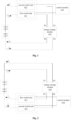
- the first switch unit and the second switch unit may have multiple specific implementations which will be illustrated by way of example below with reference to Fig. 1 to Fig. 3 , which do not belong to the present invention.
- Fig. 1 is a schematic structural diagram of a heating system provided by a first embodiment of the present disclosure.
- the heating system may include a battery pack, a control module 101, an energy storage module 102, a first switch unit K1, and a second switch unit K2.
- the energy storage module 102 may include four connection ports P1-P4.
- the first switch unit K1 may be disposed between a positive electrode of the battery pack and the P1 of the energy storage module 102
- the second switch unit K2 may be disposed between the positive electrode of the battery pack and the P3 of the energy storage module 102.
- the control module 101 may control that the first switch unit K1 is switched on and the second switch unit K2 is switched off, so that the battery pack, the first switch unit K1 and the energy storage module 102 may form a discharge circuit 1.
- the flow direction of the current in the discharge circuit may be: flowing out from the positive electrode of the battery pack, passing through the first switch unit K1 and the P1 and P2 of the energy storage module 102 successively, and finally flowing back to the negative electrode of the battery pack.
- the battery pack may charge the energy storage module 102, and the current may flow through internal of the battery pack continuously, such that the battery pack may be heated.
- the control module 101 may also control that the first switch unit K1 is switched off and the second switch unit K2 is switched on, so that the energy storage module 102, the second switch unit K2, and the battery pack may form a charge circuit 2.
- the flow direction of the current in the charge circuit may be: flowing out from the P3 of the energy storage module 102, passing through the second switch unit K2, the positive electrode of the battery pack and the negative electrode of the battery pack successively, and finally flowing back to the P4 of the energy storage module 102.
- the process energy storage module 102 may charge the battery pack, and the current may flow through internal of the battery pack continuously, such that the battery pack may be heated.
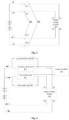
- Fig. 2 is a schematic structural diagram of a heating system provided by a second embodiment of the present disclosure.
- the difference between Fig. 2 and Fig. 1 may be that, in Fig. 2 , the first switch unit K1 is disposed between the negative electrode of the battery pack and the P2 of the energy storage module 102, and the second switch unit K2 is disposed between the negative electrode of the battery pack and the P4 of the energy storage module 102.
- the operating principle of the first switch unit K1 and the second switch unit K2 in Fig. 2 is the same as that in Fig. 1 , and details will not be described herein.
- Fig. 3 is a schematic structural diagram of a heating system provided by a third embodiment of the present disclosure.
- the difference between Fig. 3 and Fig. 1 may be that, in Fig. 3 , the first switch unit K1 may include a power switch device K11 and a power switch device K12.
- the second switch unit K2 may include a power switch device K21 and a power switch device K22.
- the battery pack, the power switch device K11, the energy storage module 102 and the power switch device K12 may form a discharge circuit 1.
- the flow direction of the current in the discharge circuit may be: flowing out from the positive electrode of the battery pack, passing through the power switch device K11, the P1 and the P2 of the energy storage module 102 and the power switch device K12 successively, and finally flowing back to the negative electrode of the battery pack.
- the battery pack may charge the energy storage module 102, and the current may flow through internal of the battery pack continuously, such that the battery pack may be heated.
- the energy storage module 102, the power switch device K21, the battery pack and the power switch device K22 may form a charge circuit 2.
- the flow direction of the current in the charge circuit may be: flowing out from the P3 of the energy storage module 102, passing through the power switch device K21, the positive electrode and the negative electrode of the battery pack and the power switch device K22 successively, and finally flowing back to the P4 of the energy storage module 102.
- the process energy storage module 102 may charge the battery pack, and the current may flow through internal of the battery pack continuously, such that the battery pack may be heated.
- the control module 101 may be required to continuously control the switching on and switching off of the first switch unit K1 and the second switch unit K2 so as to switch between the discharge circuit and the charge circuit, such that the battery pack may be heated continuously. Therefore, the switching frequency of the first switch unit K1 and the second switch unit K2 may be very high, and the current change rate may be fast when switching between the discharge circuit and the charge circuit, that is, the current direction and the current magnitude may change suddenly.
- the power switch device may be subjected to a large peak voltage, which may easily cause bad conditions (e.g. the power switch device is overheated and burned)
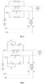
- Fig. 4 is a schematic structural diagram of a heating system provided by a fourth embodiment of the present disclosure, which may be used to describe the technical solution in the embodiment of the present disclosure in detail in conjunction with Fig. 1 .
- the heating system in the embodiment of the present disclosure may further include a buffer module.
- the buffer module may include a first buffer unit H1 and a second buffer unit H2.
- the first buffer unit H1 may be connected in parallel to both ends of the first switch unit K1 for providing a short-time path for the discharge circuit when the first switch unit K1 is being switched off.
- the second buffer unit H2 may be connected to both ends of the second switch unit K2 for providing a short-time path for the charge circuit when the second switch unit K2 is being switched off.
- the first buffer unit H1 in the embodiment of the present disclosure may provide a short-time path for the discharge circuit when the first switch unit K1 is being switched off, and the second buffer unit H2 may provide a short-time path for the charge circuit when the second switch unit K2 is being switched off, so that the voltage to which the first switch unit K1 or the second switch unit K2 are subjected may be gradually increased during the next switching on, thereby the safe and stable operation of the heating system may be guaranteed.
- the first buffer unit H1 may include a RC buffer circuit or a RCD buffer circuit, and the RC buffer circuit or the RCD buffer circuit may be connected in parallel to both ends of the first switch unit K1.
- the second buffer unit H2 may include a RC buffer circuit or a RCD buffer circuit, and the RC buffer circuit or the RCD buffer circuit may be connected in parallel to both ends of the second switch unit K2.
- Fig. 5 is a schematic structural diagram of a heating system provided by a fifth embodiment of the present disclosure.
- the first buffer unit H1 and the second buffer unit H2 shown in FIG. 5 may use a RCD circuit.
- Fig. 6 is a schematic structural diagram of a heating system provided by a sixth embodiment of the present disclosure, which belongs to the present invention. which is used to specifically show the components of the RCD circuit.
- the RCD buffer circuit may include a resistor, a capacitor, and a diode.
- the capacitor C1 when the RCD buffer circuit is connected in parallel to both ends of the first switch unit K1, a first end of the capacitor C1 is connected to a first end of the first switch unit K1, and a second end of the capacitor C1 is connected to an input end of the diode D1, an output end of the diode D1 is connected to a second end of the first switch unit K1, and the resistor R1 is connected in parallel to both ends of the capacitor C1.
- the capacitor C1 may also be referred to as an absorption capacitor.
- the buffering principle of the RCD buffer circuit to the first switch unit K1 is as follows.
- the capacitor C1 forms a discharge circuit through the resistor R1 and the first switch unit K1, and the resistor R1 consumes energy absorbed by the capacitor C1 during the switching off of the first switch unit K1, thereby the voltage fluctuation is suppressed when the first switch unit K1 is being switched on.
- the capacitor C2 may also be referred to as an absorption capacitor.
- the buffering principle of the RCD buffer circuit to the second switch unit K2 is as follows.
- the capacitor C2 forms a discharge circuit through the resistor R2 and the second switch unit K2, and the resistor R2 consumes energy absorbed by the capacitor C2 during the switching off of the second switch unit K2, thereby the voltage fluctuation is suppressed when the second switch unit K2 is being switched on.
- the diode D is a Schottky diode
- the resistance value of the resistor R is set as 0.1 ⁇ 20 ⁇
- the capacitance value of the capacitance C is set as 0.1 ⁇ 15uF.
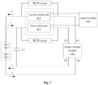
- Fig. 7 is a schematic structural diagram of a heating system provided by a seventh embodiment of the present disclosure.
- the difference between Fig. 7 and Fig. 4 may be that, the heating system of Fig. 7 may further include an absorption capacitor C3.
- the absorption capacitor C3 may be connected in parallel to the two electrodes of the battery pack.
- the working principle of the absorption capacitor C3 may be described as follows.
- the battery pack may first charge the absorption capacitor C3. Once a peak voltage generated during the switching off of the power switch device exceeds a blocking voltage of the power switch device, the peak voltage may be absorbed by a loop formed by the absorption capacitor C3 until the peak voltage and the battery pack voltage are at the same potential.
- the absorption capacitor should be a large absorption capacitor with a large voltage value.
- Fig. 8 is a schematic structural diagram of a heating system provided by an eighth embodiment of the present disclosure, which may be used to describe the technical solution in the embodiment of the present disclosure in detail in conjunction with Fig. 3 .
- the heating system of the embodiment of the present disclosure may further include a buffer module.
- the first buffer unit H1 may include two RC buffer circuits or two RCD buffer circuits, wherein one RC buffer circuit or one RCD buffer circuit may be connected in parallel to both ends of the first power switch device K11, and another RC buffer circuit or another RCD buffer circuit may be connected in parallel to both ends of the second power switch device K12.
- the second buffer unit H2 may include two RC buffer circuit or two RCD buffer circuit, wherein one RC buffer circuit or one RCD buffer circuit may be connected in parallel to both ends of the third power switch device K21, and another RC buffer circuit or another RCD buffer circuit may be connected in parallel to both ends of the fourth power switch device K22.
- K11 and K12 are used in the discharge circuit, and IGBT modules, multiple MOS tube parallel modules or SiC modules may be used due to the high switching frequency and large over current requirements.
- K21 and K22 are used in the charge circuit, and IGBT modules or SiC modules may be used, and even a quick recovery diode may be used according to functional design requirements.
- Fig. 8 further illustrates K0 used as the main switch of the heating system.
- K0 may require a low switching frequency, and may be a relay Relay, an IGBT module or a MOS.
- K11, K12, K21 and K22 may be equivalent to IGBT modules, and the application characteristics of the power switch device in the heating system will be described in detail in conjunction with Fig. 8 .
- the battery management system BMS may need to synchronously drive K11 and K12 and synchronously drive K21 and K22.
- the two IGBTs must have a timing difference of switching (on and off), making the voltage unbalanced.
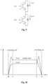
- Fig. 9 is a schematic structural diagram of two IGBTs connected in series provided by a ninth embodiment of the present disclosure, which may be used for describing the principle of voltage imbalance between the power switch devices K11 and K12, or K21 and K22.
- VT1 and VT2 are connected in series.
- the voltage between the collector C1 and the emitter E1 of VT1 may be Ucel, and the voltage between the collector C2 and the emitter E2 of VT2 may be Uce2.
- the voltage division between VT1 and VT2 may be uneven when being switched off, which may cause the switching off speeds of VT1 and VT2 being different.
- Fig. 10 is a schematic diagram illustrating changes in voltage between a collector and an emitter when VT1 and VT2 corresponding to Fig. 9 are being switched on (turned on) and switched off (turned off).
- Uce2 is first increased above the steady-state voltage and then begins to decrease, indicating that VT2 with a faster switching on speed is subjected to a higher voltage when being switched on.
- the battery pack in an on-board system, due to space constraints, the battery pack must be connected to the heating system via a certain length of wire harness. Due to the stray inductance on the power supply wire harness and the energy storage module 102, voltage overshoot may be generated when the IGBT is being switched off.
- the working voltage of K11, K12, K21, and K22 should be greater than a threshold voltage
- the threshold voltage may be a peak voltage generated due to a stray inductance of a wire harness between the battery pack and each power switch device when switching between the discharge circuit and the charge circuit.
- power switch devices of 1200V or more may be preferred on the bus vehicle.
- the voltage platform of the car vehicle may usually be 200 ⁇ 400V, and the wire harness in the car is shorter and the stray inductance is smaller, so V peak should be less than 960V.
- Power switch devices of 600-1200V may be preferred on the car vehicle platform.
- the specific design needs to be determined by actual testing.
- K11 and K12, K21 and K22 should be ideally synchronous when being switched on and off. Therefore, it is preferable to select power switch devices of the same batch, the same specification and the same manufacturer.
- a reasonable drive circuit may need to implement the function of preventing the IGBT from short circuit and overvoltage.
- the implementation of the drive circuit of the IGBT will be described in detail below.
- the drive circuit of the IGBT may first need to consider the maximum peak current I max of the IGBT.
- the maximum peak current I max of the IGBT may be estimated using equation (3).
- I max is the peak current output by the driver IC
- U gemax is the positive gate voltage of the IGBT when being switched on
- U gemin is the negative gate voltage of the IGBT when being switched off
- the value of U gemax and U gemin is generally in the range of -20V ⁇ +20V
- R gin is the internal gate resistance of the IGBT which is in the range of 0.8-1.2 S2
- R gext is the gate resistance applied by the external drive circuit.
- R gext is one of the key parts of the design of the drive circuit.
- the switching performance and loss of the IGBT depends on the value of R gext . Therefore, the value of R gext needs to be selected according to different types of IGBTs and dynamically adjusted by actual testing.
- Equation (3) 0.74 is a correction factor, and the derivation process may be as follows.
- L L gon + L goff which is the sum of the stray inductances of the lead wire of the gate
- R g R gin + R gext which is the sum of the internal and external gate resistances
- i g ( t ) is the gate current that changes over time.
- 2 e is the correction factor which equals to 0.74;
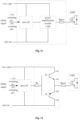
- Fig. 11 is a schematic structural diagram of a power switch device provided by a tenth embodiment of the present disclosure.
- the power switch device may include an IGBT and a drive circuit for driving the IGBT.
- the drive circuit may include a drive IC and an external gate resistor R gext connected to the drive IC, the external gate resistor R gext is connected to the gate G of the IGBT.
- the heating system may further include a power amplification module 1101 for meeting a demand for the power switch device (e.g., the IGBT) for a large drive current.
- a power amplification module 1101 for meeting a demand for the power switch device (e.g., the IGBT) for a large drive current.
- the power amplification module 1101 may be disposed between the drive IC and the external gate resistor R gext , and the power amplification module 1101 may include a single-stage or multi-stage power amplification circuit for amplifying a current output by the drive IC to meet the demand of the IGBT for a large drive current.
- Fig. 12 is a schematic structural diagram of a power switch device provided by an eleventh embodiment of the present disclosure, which is used to illustrate the specific components of a power amplification circuit.
- the power amplification circuit may include a NPN triode and a PNP triode.
- an output end of the drive IC may be respectively connected to a base B1 of the NPN triode and a base B2 of the PNP triode.
- a collector C01 of the NPN triode may be respectively connected to a positive DC voltage source (+5V-+20V) and the drive IC.
- a collector C02 of the PNP triode may be respectively connected to a negative DC voltage source (-20V ⁇ 0V) and the drive IC.
- An emitter of the NPN triode and an emitter of the PNP triode are both connected to the external gate resistor R gext .
- the power amplification circuit may further include an amplification resistor Rc.
- One end of the amplification resistor Rc may be connected to the output end of the drive IC, and another end of the amplification resistor Rc may be respectively connected to the base B1 of the NPN transistor and the base B2 of the PNP transistor.
- the working principle of the power amplification circuit shown in FIG. 12 may be as follows.
- the drive IC When the drive IC receives a high-level switching on signal (+5V) of the control module 101, it may output a positive drive current to Rc, and the collector C01 and the emitter E01 of the NPN transistor may be switched on, such that the level between the gate G and the emitter E of the IGBT may be pulled to +5V ⁇ +20V, resulting that the IGBT is switched on.
- the drive IC When the drive IC receives a low-level switching off signal (0V) of the control module 101, it may output a negative drive current to Rc, and the collector C02 and the emitter E02 of the PNP transistor may be switched off, such that the level between the gate G and the emitter E of the IGBT may be pulled to -20V ⁇ 0V, resulting that the IGBT is switched off.
- a low-level switching off signal (0V) of the control module 101 it may output a negative drive current to Rc, and the collector C02 and the emitter E02 of the PNP transistor may be switched off, such that the level between the gate G and the emitter E of the IGBT may be pulled to -20V ⁇ 0V, resulting that the IGBT is switched off.
- Fig. 12 only illustrates the topological structure of the single-stage power amplification circuit.
- the driving capability for the IGBT may further be improved via the multi-stage power amplification circuit.
- those skilled in the art may also implement driving of the IGBT by using other types of power amplification circuits according to actual needs, which is not limited herein.
- the peak current I max required to drive the IGBT may be calculated using the formula (3).
- the NPN and PNP of large package may be selected, and the maximum current of each boost stage may be considered. If there is only one boost stage, the maximum current and the peak current obtained by S1 may be the same; If there are multiple boost stages, multiple boost stages may be connected in parallel, and the resistance value of the R gext may be calculated according to the current supplied by each boost stage and the number of the boost stages.
- the current transmission ratio h e of the triode may be determined according to the data sheet of the selected NPN and PNP, the base current I b1 of the NPN transistor and the base current I b 2 of the PNP transistor may be calculated using I peak h e , and then the resistance value of the R c may be calculated according to the voltage value ⁇ V ge used for driving the IGBT.
- the voltage division of the devices may be uneven due to the different synchronization characteristics of K11 and K12. Therefore, the drive ICs and the drive circuits of K11 and K12 should be identical in design.
- the PCB design should also be highly symmetric, and the wire between the drive board and the IGBT should be as symmetric as possible.
- the value of the drive resistor should be corrected according to the actual testing. In the present design, the value of R gext may be set as 1.5-3.8Q, the value of R c may be set as 30-180Q.
- the use of the power switch device is slightly different from that of other conventional systems.
- the three measures mentioned above are not used separately in the system, and are combined to implement the application of the large power switch device in the rapid heating system of the battery pack.
- the functional blocks shown in the block diagrams described above may be implemented as hardware, software, firmware, or a combination thereof.
- it may be, for example, an electronic circuit, an application specific integrated circuit (ASIC), suitable firmware, plug-ins, function cards, and the like.
- ASIC application specific integrated circuit
- the elements of an embodiment of the present disclosure are programs or code segments that are used to perform the required tasks.
- Programs or code segments may be stored on a machine-readable medium or transmitted over a transmission medium or communication link via a data signal carried in a carrier wave.
- the "machine-readable medium” may include any medium that is capable of storing or transmitting information.
- machine-readable media examples include electronic circuitry, semiconductor memory devices, ROMs, flash memory, erasable ROM (EROM), floppy disks, CD-ROMs, optical disks, hard disks, fiber optic media, radio frequency (RF) links, and the like.
- the code segments may be downloaded via a computer network such as the Internet, an intranet or the like.
Landscapes
- Engineering & Computer Science (AREA)
- Manufacturing & Machinery (AREA)
- Chemical & Material Sciences (AREA)
- Chemical Kinetics & Catalysis (AREA)
- Electrochemistry (AREA)
- General Chemical & Material Sciences (AREA)
- Power Engineering (AREA)
- Microelectronics & Electronic Packaging (AREA)
- Automation & Control Theory (AREA)
- Secondary Cells (AREA)
- Charge And Discharge Circuits For Batteries Or The Like (AREA)
- Supply And Distribution Of Alternating Current (AREA)
Claims (2)
- Heizsystem, umfassend: einen Batteriepack, ein Energiespeichermodul (102), ein Schaltmodul, ein Steuermodul (101) und ein Puffermodul; wobeidas Schaltmodul eine erste Schalteinheit (K1) und eine zweite Schalteinheit (K2) umfasst;das Steuermodul (101) steuert, dass die erste Schalteinheit (K1) eingeschaltet und die zweite Schalteinheit (K2) ausgeschaltet wird, so dass der Batteriepack, die erste Schalteinheit (K1) und das Energiespeichermodul (102) einen Entladekreis (1) bilden;das Steuermodul (101) steuert, dass die erste Schalteinheit (K1) ausgeschaltet und die zweite Schalteinheit (K2) eingeschaltet wird, so dass das Energiespeichermodul (102), die zweite Schalteinheit (K2) und der Batteriepack einen Ladekreis (2) bilden;das Puffermodul eine erste Puffereinheit (H1) und eine zweite Puffereinheit (H2) umfasst, wobei die erste Puffereinheit (H1) parallel zu beiden Enden der ersten Schalteinheit (K1) geschaltet ist, um einen Kurzzeitpfad beim Einschalten oder Ausschalten der ersten Schalteinheit (K1) bereitzustellen; und die zweite Puffereinheit (H2) parallel zu beiden Enden der zweiten Schalteinheit (K2) geschaltet ist, um einen Kurzzeitpfad beim Einschalten oder Ausschalten der zweiten Schalteinheit (K2) bereitzustellen,das Heizsystem dadurch gekennzeichnet ist, dass:die erste Puffereinheit (H1) einen ersten RCD-Pufferkreis umfasst, und der erste RCD-Pufferkreis parallel zu beiden Enden der ersten Schaltereinheit (K1) geschaltet ist;die zweite Puffereinheit (H2) einen zweiten RCD-Pufferkreis umfasst, und der zweite RCD-Pufferkreis parallel zu beiden Enden der zweiten Schalteinheit (K2) geschaltet ist,wobei der erste RCD-Pufferkreis einen ersten Widerstand (R1), einen ersten Kondensator (C1) und eine erste Diode (D1) umfasst, der zweite RCD-Pufferkreis einen zweiten Widerstand (R2), einen zweiten Kondensator (C2) und eine zweite Diode (D2) umfasst, die erste Diode (D1) und die zweite Diode (D2) beide Schottky-Dioden sind, die Widerstandswerte des ersten Widerstands (R1) und des zweiten Widerstands (R2) innerhalb eines Bereichs von 0,1Ω bis 20Ω liegen, und die Kapazitätswerte des ersten Kondensators (Cf) und des zweiten Kondensators (C2) in einem Bereich von 0,1uF bis 15uF liegen;wobei der erste RCD-Pufferkreis parallel zu beiden Enden der ersten Schalteinheit (K1) geschaltet ist, ein erstes Ende des ersten Kondensators (C1) mit einem ersten Ende der ersten Schalteinheit (K1) geschaltet ist, ein zweites Ende des ersten Kondensators (C1) mit einem Eingangsende der ersten Diode (D1) geschaltet ist, ein Ausgangsende der ersten Diode (D1) mit einem zweiten Ende der ersten Schalteinheit (K1) geschaltet ist, und der erste Widerstand (R1) parallel zu beiden Enden des ersten Kondensators (C1) geschaltet ist;wobei der zweite RCD-Pufferkreis parallel zu beiden Enden der zweiten Schalteinheit (K2) geschaltet ist, ein erstes Ende des zweiten Kondensators (C2) mit einem ersten Ende der zweiten Schalteinheit (K2) geschaltet ist, ein zweites Ende des zweiten Kondensators (C2) mit einem Ausgangsende der zweiten Diode (D2) geschaltet ist, ein Eingangsende der zweiten Diode (D2) mit einem zweiten Ende der zweiten Schalteinheit (K2) geschaltet ist, und der zweite Widerstand (R2) parallel zu beiden Enden des zweiten Kondensators (C2) geschaltet ist;.wobei eine minimale Einschaltzeit einer Leistungsschalteinrichtung in der ersten Schalteinheit (K1) durch eine Zeitkonstante


- Heizsystem nach Anspruch 1, wobei das Heizsystem ferner einen Absorptionskondensator (C3) umfasst, der parallel zu zwei Elektroden des Batteriepacks geschaltet ist.
Applications Claiming Priority (1)
| Application Number | Priority Date | Filing Date | Title |
|---|---|---|---|
| CN201810495005.4A CN108879027B (zh) | 2018-05-22 | 2018-05-22 | 加热系统和功率开关器件 |
Publications (3)
| Publication Number | Publication Date |
|---|---|
| EP3573173A2 EP3573173A2 (de) | 2019-11-27 |
| EP3573173A3 EP3573173A3 (de) | 2019-12-25 |
| EP3573173B1 true EP3573173B1 (de) | 2023-08-23 |
Family
ID=64334018
Family Applications (1)
| Application Number | Title | Priority Date | Filing Date |
|---|---|---|---|
| EP19150228.5A Active EP3573173B1 (de) | 2018-05-22 | 2019-01-03 | Heizsystem mit leistungsschaltervorrichtung |
Country Status (4)
| Country | Link |
|---|---|
| US (1) | US10847987B2 (de) |
| EP (1) | EP3573173B1 (de) |
| CN (1) | CN108879027B (de) |
| ES (1) | ES2956790T3 (de) |
Families Citing this family (16)
| Publication number | Priority date | Publication date | Assignee | Title |
|---|---|---|---|---|
| CN110970961B (zh) | 2018-12-06 | 2021-06-08 | 宁德时代新能源科技股份有限公司 | 用电保护电路 |
| CN110970882A (zh) | 2018-12-24 | 2020-04-07 | 宁德时代新能源科技股份有限公司 | 一种保护电路及电池管理系统 |
| CN117614091A (zh) * | 2019-04-01 | 2024-02-27 | 福州欣联达电子科技有限公司 | 一种电流可控的单双向开关电路及其控制方法 |
| CN110299744B (zh) * | 2019-07-08 | 2021-12-10 | 阳光电源股份有限公司 | 一种高压电池簇及其过流保护电路和开关盒 |
| KR102699008B1 (ko) | 2019-08-30 | 2024-08-26 | 현대자동차주식회사 | 모터 구동 시스템을 이용한 배터리 승온 시스템 및 방법 |
| CN111431407A (zh) * | 2020-03-24 | 2020-07-17 | 珠海格力电器股份有限公司 | 直流升压变换器、电源系统及电动汽车 |
| KR20220026970A (ko) | 2020-08-26 | 2022-03-07 | 현대자동차주식회사 | 모터 구동 시스템을 이용한 배터리 승온 시스템 및 방법 |
| KR20220089347A (ko) | 2020-12-21 | 2022-06-28 | 현대자동차주식회사 | 모터 구동 시스템을 이용한 배터리 승온 시스템 및 방법 |
| CN114714981B (zh) * | 2021-01-05 | 2025-07-11 | 广汽埃安新能源汽车股份有限公司 | 电池加热的电路、系统以及方法 |
| CN113629820B (zh) * | 2021-09-02 | 2024-08-02 | 阳光储能技术有限公司 | 一种电池模组、储能系统及其控制方法 |
| CN114050330B (zh) * | 2021-10-11 | 2024-06-25 | 华为数字能源技术有限公司 | 电池系统及供电系统 |
| EP4276980A4 (de) | 2021-11-15 | 2025-03-26 | Contemporary Amperex Technology (Hong Kong) Limited | Batterieerwärmungsschaltung und steuerungsverfahren dafür, batterie und elektrofahrzeug |
| CN114744722A (zh) * | 2022-04-28 | 2022-07-12 | 深圳市道通智能航空技术股份有限公司 | 一种供电电路和用电设备 |
| CN114938046A (zh) * | 2022-05-19 | 2022-08-23 | 华为数字能源技术有限公司 | 一种储能装置及其控制方法、以及光伏系统 |
| CN117220480B (zh) * | 2023-08-08 | 2025-02-07 | 浙江吉利控股集团有限公司 | 一种功率器件的保护电路及其驱动方法、电源装置 |
| CN118472493B (zh) * | 2024-07-12 | 2024-11-19 | 荣耀终端有限公司 | 电子设备及其控制方法、充电系统 |
Family Cites Families (13)
| Publication number | Priority date | Publication date | Assignee | Title |
|---|---|---|---|---|
| JP2009071956A (ja) * | 2007-09-12 | 2009-04-02 | Mitsubishi Electric Corp | ゲート駆動回路 |
| US8452490B2 (en) * | 2009-12-14 | 2013-05-28 | Control Solutions LLC | Electronic circuit for charging and heating a battery |
| KR101230353B1 (ko) | 2010-01-28 | 2013-02-06 | 주식회사 엘지화학 | 전지 내부 저항을 이용한 저온 성능 개선 전지팩 시스템 |
| CN102082306B (zh) * | 2010-07-30 | 2012-11-21 | 比亚迪股份有限公司 | 一种电池的加热电路 |
| US9160041B2 (en) | 2010-07-30 | 2015-10-13 | Byd Company Limited | Battery heating circuits and methods using resonance components in series and bridging charge storage components |
| US8749278B2 (en) * | 2010-08-09 | 2014-06-10 | Honda Motor Co., Ltd. | Semiconductor device driving unit and method |
| US9065293B2 (en) | 2010-12-23 | 2015-06-23 | Byd Company Limited | Battery heating circuits and methods using transformers |
| CN102074752B (zh) * | 2010-12-23 | 2012-07-04 | 比亚迪股份有限公司 | 一种电池的加热电路 |
| TWI501507B (zh) * | 2012-07-13 | 2015-09-21 | 蔡富生 | 藉助於虛擬電池機制來進行電池單元控制之方法與裝置 |
| CN203721843U (zh) * | 2014-01-07 | 2014-07-16 | 同济大学 | 一种动力锂离子电池模块用低温自加热电路 |
| US20180191339A1 (en) | 2014-03-20 | 2018-07-05 | Tm4 Inc. | Gate Driver Controlling a Collector to Emitter Voltage Variation of an electronic Switch and Circuits Including the Gate Driver |
| CN104638318B (zh) | 2014-11-28 | 2016-11-09 | 富奥汽车零部件股份有限公司 | 一种电动车动力电池组低温快速加热方法及系统 |
| KR101639488B1 (ko) | 2014-12-10 | 2016-07-13 | 현대모비스 주식회사 | 암 쇼트 방지를 위한 게이트 구동 회로 및 방법 |
-
2018
- 2018-05-22 CN CN201810495005.4A patent/CN108879027B/zh active Active
- 2018-12-28 US US16/235,274 patent/US10847987B2/en active Active
-
2019
- 2019-01-03 ES ES19150228T patent/ES2956790T3/es active Active
- 2019-01-03 EP EP19150228.5A patent/EP3573173B1/de active Active
Also Published As
| Publication number | Publication date |
|---|---|
| US20190363562A1 (en) | 2019-11-28 |
| CN108879027A (zh) | 2018-11-23 |
| EP3573173A3 (de) | 2019-12-25 |
| ES2956790T3 (es) | 2023-12-28 |
| US10847987B2 (en) | 2020-11-24 |
| CN108879027B (zh) | 2021-08-17 |
| EP3573173A2 (de) | 2019-11-27 |
Similar Documents
| Publication | Publication Date | Title |
|---|---|---|
| EP3573173B1 (de) | Heizsystem mit leistungsschaltervorrichtung | |
| KR101273820B1 (ko) | 전원 장치 | |
| US10236677B2 (en) | Semiconductor device | |
| EP2404359B1 (de) | Systeme und verfahren zur skalierbaren konfiguration intelligenter energiespeicherpacks | |
| CN105122578B (zh) | 均衡补正装置以及蓄电装置 | |
| US8972158B2 (en) | Semiconductor device providing a current control function and a self shut down function | |
| US20130057218A1 (en) | Device and method for controlling charge of assembled battery | |
| CN213846230U (zh) | 一种过流保护电路 | |
| CN112491255B (zh) | 均压电路、飞跨电容三电平变换器及设备 | |
| CN111883085B (zh) | 一种改善液晶设备稳定工作的装置 | |
| CN219960175U (zh) | 管理系统、电源设备和车辆 | |
| KR101089206B1 (ko) | 전계효과 트랜지스터의 구동기 회로 | |
| CN117220480B (zh) | 一种功率器件的保护电路及其驱动方法、电源装置 | |
| CN119210416A (zh) | 一种SiC MOSFET驱动电路及其控制方法 | |
| CN118539381A (zh) | 一种电源保护电路和储能电源 | |
| JP2017046371A (ja) | 電圧制御回路 | |
| JP2006050865A (ja) | 半導体電力変換装置の駆動回路 | |
| US12206328B2 (en) | DC-DC converter and power supply device | |
| CN209767182U (zh) | 电池保护电路 | |
| CN212541261U (zh) | 一种关机复位电路、电子设备 | |
| CN223093499U (zh) | 保护电路和电池管理系统 | |
| US20260081519A1 (en) | Methods, apparatuses, and systems for discharging electronic devices | |
| CN220492637U (zh) | 一种防正负浪涌电流冲击的抑制电路 | |
| CN223309620U (zh) | 一种限流电路及电池包 | |
| US20250350281A1 (en) | Gate driver circuit and operating method thereof |
Legal Events
| Date | Code | Title | Description |
|---|---|---|---|
| PUAI | Public reference made under article 153(3) epc to a published international application that has entered the european phase |
Free format text: ORIGINAL CODE: 0009012 |
|
| STAA | Information on the status of an ep patent application or granted ep patent |
Free format text: STATUS: THE APPLICATION HAS BEEN PUBLISHED |
|
| PUAL | Search report despatched |
Free format text: ORIGINAL CODE: 0009013 |
|
| AK | Designated contracting states |
Kind code of ref document: A2 Designated state(s): AL AT BE BG CH CY CZ DE DK EE ES FI FR GB GR HR HU IE IS IT LI LT LU LV MC MK MT NL NO PL PT RO RS SE SI SK SM TR |
|
| AX | Request for extension of the european patent |
Extension state: BA ME |
|
| AK | Designated contracting states |
Kind code of ref document: A3 Designated state(s): AL AT BE BG CH CY CZ DE DK EE ES FI FR GB GR HR HU IE IS IT LI LT LU LV MC MK MT NL NO PL PT RO RS SE SI SK SM TR |
|
| AX | Request for extension of the european patent |
Extension state: BA ME |
|
| RIC1 | Information provided on ipc code assigned before grant |
Ipc: H03K 17/081 20060101ALI20191118BHEP Ipc: H01M 10/615 20140101AFI20191118BHEP Ipc: H01M 10/637 20140101ALI20191118BHEP |
|
| STAA | Information on the status of an ep patent application or granted ep patent |
Free format text: STATUS: REQUEST FOR EXAMINATION WAS MADE |
|
| 17P | Request for examination filed |
Effective date: 20200330 |
|
| RBV | Designated contracting states (corrected) |
Designated state(s): AL AT BE BG CH CY CZ DE DK EE ES FI FR GB GR HR HU IE IS IT LI LT LU LV MC MK MT NL NO PL PT RO RS SE SI SK SM TR |
|
| STAA | Information on the status of an ep patent application or granted ep patent |
Free format text: STATUS: EXAMINATION IS IN PROGRESS |
|
| 17Q | First examination report despatched |
Effective date: 20201006 |
|
| RIC1 | Information provided on ipc code assigned before grant |
Ipc: H03K 17/0812 20060101ALI20230402BHEP Ipc: H01M 10/637 20140101ALI20230402BHEP Ipc: H03K 17/081 20060101ALI20230402BHEP Ipc: H01M 10/615 20140101AFI20230402BHEP |
|
| GRAP | Despatch of communication of intention to grant a patent |
Free format text: ORIGINAL CODE: EPIDOSNIGR1 |
|
| STAA | Information on the status of an ep patent application or granted ep patent |
Free format text: STATUS: GRANT OF PATENT IS INTENDED |
|
| INTG | Intention to grant announced |
Effective date: 20230605 |
|
| RIN1 | Information on inventor provided before grant (corrected) |
Inventor name: ZHU, TAOSHENG Inventor name: WU, XINGYUAN Inventor name: ZUO, XIYANG Inventor name: HOU, YIZHEN Inventor name: ZHANG, WEI Inventor name: DAN, ZHIMIN |
|
| GRAS | Grant fee paid |
Free format text: ORIGINAL CODE: EPIDOSNIGR3 |
|
| GRAA | (expected) grant |
Free format text: ORIGINAL CODE: 0009210 |
|
| STAA | Information on the status of an ep patent application or granted ep patent |
Free format text: STATUS: THE PATENT HAS BEEN GRANTED |
|
| AK | Designated contracting states |
Kind code of ref document: B1 Designated state(s): AL AT BE BG CH CY CZ DE DK EE ES FI FR GB GR HR HU IE IS IT LI LT LU LV MC MK MT NL NO PL PT RO RS SE SI SK SM TR |
|
| REG | Reference to a national code |
Ref country code: GB Ref legal event code: FG4D |
|
| REG | Reference to a national code |
Ref country code: CH Ref legal event code: EP |
|
| REG | Reference to a national code |
Ref country code: IE Ref legal event code: FG4D |
|
| REG | Reference to a national code |
Ref country code: DE Ref legal event code: R096 Ref document number: 602019035387 Country of ref document: DE |
|
| REG | Reference to a national code |
Ref country code: NL Ref legal event code: FP |
|
| P01 | Opt-out of the competence of the unified patent court (upc) registered |
Effective date: 20230908 |
|
| REG | Reference to a national code |
Ref country code: NO Ref legal event code: T2 Effective date: 20230823 |
|
| REG | Reference to a national code |
Ref country code: LT Ref legal event code: MG9D |
|
| REG | Reference to a national code |
Ref country code: ES Ref legal event code: FG2A Ref document number: 2956790 Country of ref document: ES Kind code of ref document: T3 Effective date: 20231228 |
|
| REG | Reference to a national code |
Ref country code: AT Ref legal event code: MK05 Ref document number: 1603654 Country of ref document: AT Kind code of ref document: T Effective date: 20230823 |
|
| PG25 | Lapsed in a contracting state [announced via postgrant information from national office to epo] |
Ref country code: GR Free format text: LAPSE BECAUSE OF FAILURE TO SUBMIT A TRANSLATION OF THE DESCRIPTION OR TO PAY THE FEE WITHIN THE PRESCRIBED TIME-LIMIT Effective date: 20231124 |
|
| PG25 | Lapsed in a contracting state [announced via postgrant information from national office to epo] |
Ref country code: IS Free format text: LAPSE BECAUSE OF FAILURE TO SUBMIT A TRANSLATION OF THE DESCRIPTION OR TO PAY THE FEE WITHIN THE PRESCRIBED TIME-LIMIT Effective date: 20231223 |
|
| PG25 | Lapsed in a contracting state [announced via postgrant information from national office to epo] |
Ref country code: SE Free format text: LAPSE BECAUSE OF FAILURE TO SUBMIT A TRANSLATION OF THE DESCRIPTION OR TO PAY THE FEE WITHIN THE PRESCRIBED TIME-LIMIT Effective date: 20230823 Ref country code: RS Free format text: LAPSE BECAUSE OF FAILURE TO SUBMIT A TRANSLATION OF THE DESCRIPTION OR TO PAY THE FEE WITHIN THE PRESCRIBED TIME-LIMIT Effective date: 20230823 Ref country code: PT Free format text: LAPSE BECAUSE OF FAILURE TO SUBMIT A TRANSLATION OF THE DESCRIPTION OR TO PAY THE FEE WITHIN THE PRESCRIBED TIME-LIMIT Effective date: 20231226 Ref country code: LV Free format text: LAPSE BECAUSE OF FAILURE TO SUBMIT A TRANSLATION OF THE DESCRIPTION OR TO PAY THE FEE WITHIN THE PRESCRIBED TIME-LIMIT Effective date: 20230823 Ref country code: LT Free format text: LAPSE BECAUSE OF FAILURE TO SUBMIT A TRANSLATION OF THE DESCRIPTION OR TO PAY THE FEE WITHIN THE PRESCRIBED TIME-LIMIT Effective date: 20230823 Ref country code: IS Free format text: LAPSE BECAUSE OF FAILURE TO SUBMIT A TRANSLATION OF THE DESCRIPTION OR TO PAY THE FEE WITHIN THE PRESCRIBED TIME-LIMIT Effective date: 20231223 Ref country code: HR Free format text: LAPSE BECAUSE OF FAILURE TO SUBMIT A TRANSLATION OF THE DESCRIPTION OR TO PAY THE FEE WITHIN THE PRESCRIBED TIME-LIMIT Effective date: 20230823 Ref country code: GR Free format text: LAPSE BECAUSE OF FAILURE TO SUBMIT A TRANSLATION OF THE DESCRIPTION OR TO PAY THE FEE WITHIN THE PRESCRIBED TIME-LIMIT Effective date: 20231124 Ref country code: FI Free format text: LAPSE BECAUSE OF FAILURE TO SUBMIT A TRANSLATION OF THE DESCRIPTION OR TO PAY THE FEE WITHIN THE PRESCRIBED TIME-LIMIT Effective date: 20230823 Ref country code: AT Free format text: LAPSE BECAUSE OF FAILURE TO SUBMIT A TRANSLATION OF THE DESCRIPTION OR TO PAY THE FEE WITHIN THE PRESCRIBED TIME-LIMIT Effective date: 20230823 |
|
| PG25 | Lapsed in a contracting state [announced via postgrant information from national office to epo] |
Ref country code: PL Free format text: LAPSE BECAUSE OF FAILURE TO SUBMIT A TRANSLATION OF THE DESCRIPTION OR TO PAY THE FEE WITHIN THE PRESCRIBED TIME-LIMIT Effective date: 20230823 |
|
| PG25 | Lapsed in a contracting state [announced via postgrant information from national office to epo] |
Ref country code: SM Free format text: LAPSE BECAUSE OF FAILURE TO SUBMIT A TRANSLATION OF THE DESCRIPTION OR TO PAY THE FEE WITHIN THE PRESCRIBED TIME-LIMIT Effective date: 20230823 Ref country code: RO Free format text: LAPSE BECAUSE OF FAILURE TO SUBMIT A TRANSLATION OF THE DESCRIPTION OR TO PAY THE FEE WITHIN THE PRESCRIBED TIME-LIMIT Effective date: 20230823 Ref country code: EE Free format text: LAPSE BECAUSE OF FAILURE TO SUBMIT A TRANSLATION OF THE DESCRIPTION OR TO PAY THE FEE WITHIN THE PRESCRIBED TIME-LIMIT Effective date: 20230823 Ref country code: DK Free format text: LAPSE BECAUSE OF FAILURE TO SUBMIT A TRANSLATION OF THE DESCRIPTION OR TO PAY THE FEE WITHIN THE PRESCRIBED TIME-LIMIT Effective date: 20230823 Ref country code: CZ Free format text: LAPSE BECAUSE OF FAILURE TO SUBMIT A TRANSLATION OF THE DESCRIPTION OR TO PAY THE FEE WITHIN THE PRESCRIBED TIME-LIMIT Effective date: 20230823 Ref country code: SK Free format text: LAPSE BECAUSE OF FAILURE TO SUBMIT A TRANSLATION OF THE DESCRIPTION OR TO PAY THE FEE WITHIN THE PRESCRIBED TIME-LIMIT Effective date: 20230823 |
|
| REG | Reference to a national code |
Ref country code: DE Ref legal event code: R097 Ref document number: 602019035387 Country of ref document: DE |
|
| PLBE | No opposition filed within time limit |
Free format text: ORIGINAL CODE: 0009261 |
|
| STAA | Information on the status of an ep patent application or granted ep patent |
Free format text: STATUS: NO OPPOSITION FILED WITHIN TIME LIMIT |
|
| 26N | No opposition filed |
Effective date: 20240524 |
|
| PG25 | Lapsed in a contracting state [announced via postgrant information from national office to epo] |
Ref country code: SI Free format text: LAPSE BECAUSE OF FAILURE TO SUBMIT A TRANSLATION OF THE DESCRIPTION OR TO PAY THE FEE WITHIN THE PRESCRIBED TIME-LIMIT Effective date: 20230823 |
|
| REG | Reference to a national code |
Ref country code: DE Ref legal event code: R081 Ref document number: 602019035387 Country of ref document: DE Owner name: CONTEMPORARY AMPEREX TECHNOLOGY (HONG KONG) LI, HK Free format text: FORMER OWNER: CONTEMPORARY AMPEREX TECHNOLOGY CO., LIMITED, NINGDE CITY, FUJIAN, CN |
|
| PG25 | Lapsed in a contracting state [announced via postgrant information from national office to epo] |
Ref country code: MC Free format text: LAPSE BECAUSE OF FAILURE TO SUBMIT A TRANSLATION OF THE DESCRIPTION OR TO PAY THE FEE WITHIN THE PRESCRIBED TIME-LIMIT Effective date: 20230823 |
|
| REG | Reference to a national code |
Ref country code: NL Ref legal event code: PD Owner name: CONTEMPORARY AMPEREX TECHNOLOGY (HONG KONG) LIMITED; CN Free format text: DETAILS ASSIGNMENT: CHANGE OF OWNER(S), ASSIGNMENT; FORMER OWNER NAME: CONTEMPORARY AMPEREX TECHNOLOGY CO., LIMITED Effective date: 20240819 |
|
| PG25 | Lapsed in a contracting state [announced via postgrant information from national office to epo] |
Ref country code: MC Free format text: LAPSE BECAUSE OF FAILURE TO SUBMIT A TRANSLATION OF THE DESCRIPTION OR TO PAY THE FEE WITHIN THE PRESCRIBED TIME-LIMIT Effective date: 20230823 |
|
| REG | Reference to a national code |
Ref country code: CH Ref legal event code: PL |
|
| REG | Reference to a national code |
Ref country code: GB Ref legal event code: 732E Free format text: REGISTERED BETWEEN 20240815 AND 20240821 |
|
| PG25 | Lapsed in a contracting state [announced via postgrant information from national office to epo] |
Ref country code: LU Free format text: LAPSE BECAUSE OF NON-PAYMENT OF DUE FEES Effective date: 20240103 |
|
| PG25 | Lapsed in a contracting state [announced via postgrant information from national office to epo] |
Ref country code: LU Free format text: LAPSE BECAUSE OF NON-PAYMENT OF DUE FEES Effective date: 20240103 |
|
| PG25 | Lapsed in a contracting state [announced via postgrant information from national office to epo] |
Ref country code: BE Free format text: LAPSE BECAUSE OF NON-PAYMENT OF DUE FEES Effective date: 20240131 |
|
| PG25 | Lapsed in a contracting state [announced via postgrant information from national office to epo] |
Ref country code: CH Free format text: LAPSE BECAUSE OF NON-PAYMENT OF DUE FEES Effective date: 20240131 |
|
| PG25 | Lapsed in a contracting state [announced via postgrant information from national office to epo] |
Ref country code: CH Free format text: LAPSE BECAUSE OF NON-PAYMENT OF DUE FEES Effective date: 20240131 Ref country code: BE Free format text: LAPSE BECAUSE OF NON-PAYMENT OF DUE FEES Effective date: 20240131 |
|
| REG | Reference to a national code |
Ref country code: BE Ref legal event code: MM Effective date: 20240131 |
|
| PG25 | Lapsed in a contracting state [announced via postgrant information from national office to epo] |
Ref country code: BG Free format text: LAPSE BECAUSE OF FAILURE TO SUBMIT A TRANSLATION OF THE DESCRIPTION OR TO PAY THE FEE WITHIN THE PRESCRIBED TIME-LIMIT Effective date: 20230823 |
|
| PG25 | Lapsed in a contracting state [announced via postgrant information from national office to epo] |
Ref country code: BG Free format text: LAPSE BECAUSE OF FAILURE TO SUBMIT A TRANSLATION OF THE DESCRIPTION OR TO PAY THE FEE WITHIN THE PRESCRIBED TIME-LIMIT Effective date: 20230823 |
|
| REG | Reference to a national code |
Ref country code: ES Ref legal event code: PC2A Owner name: CONTEMPORARY AMPEREX TECHNOLOGY (HONG KONG) LIMITED Effective date: 20241129 |
|
| PG25 | Lapsed in a contracting state [announced via postgrant information from national office to epo] |
Ref country code: IE Free format text: LAPSE BECAUSE OF NON-PAYMENT OF DUE FEES Effective date: 20240103 |
|
| PG25 | Lapsed in a contracting state [announced via postgrant information from national office to epo] |
Ref country code: IE Free format text: LAPSE BECAUSE OF NON-PAYMENT OF DUE FEES Effective date: 20240103 |
|
| PG25 | Lapsed in a contracting state [announced via postgrant information from national office to epo] |
Ref country code: CY Free format text: LAPSE BECAUSE OF FAILURE TO SUBMIT A TRANSLATION OF THE DESCRIPTION OR TO PAY THE FEE WITHIN THE PRESCRIBED TIME-LIMIT; INVALID AB INITIO Effective date: 20190103 |
|
| PG25 | Lapsed in a contracting state [announced via postgrant information from national office to epo] |
Ref country code: HU Free format text: LAPSE BECAUSE OF FAILURE TO SUBMIT A TRANSLATION OF THE DESCRIPTION OR TO PAY THE FEE WITHIN THE PRESCRIBED TIME-LIMIT; INVALID AB INITIO Effective date: 20190103 |
|
| PG25 | Lapsed in a contracting state [announced via postgrant information from national office to epo] |
Ref country code: TR Free format text: LAPSE BECAUSE OF FAILURE TO SUBMIT A TRANSLATION OF THE DESCRIPTION OR TO PAY THE FEE WITHIN THE PRESCRIBED TIME-LIMIT Effective date: 20230823 |
|
| PGFP | Annual fee paid to national office [announced via postgrant information from national office to epo] |
Ref country code: NL Payment date: 20251126 Year of fee payment: 8 |
|
| PGFP | Annual fee paid to national office [announced via postgrant information from national office to epo] |
Ref country code: GB Payment date: 20251120 Year of fee payment: 8 |
|
| PGFP | Annual fee paid to national office [announced via postgrant information from national office to epo] |
Ref country code: FR Payment date: 20251124 Year of fee payment: 8 |
|
| PGFP | Annual fee paid to national office [announced via postgrant information from national office to epo] |
Ref country code: ES Payment date: 20260213 Year of fee payment: 8 |
|
| PGFP | Annual fee paid to national office [announced via postgrant information from national office to epo] |
Ref country code: NO Payment date: 20260109 Year of fee payment: 8 Ref country code: DE Payment date: 20251119 Year of fee payment: 8 |
|
| PGFP | Annual fee paid to national office [announced via postgrant information from national office to epo] |
Ref country code: IT Payment date: 20251219 Year of fee payment: 8 |