EP3572968B1 - Clock-gating-einheit für einen transponder - Google Patents
Clock-gating-einheit für einen transponder Download PDFInfo
- Publication number
- EP3572968B1 EP3572968B1 EP18173666.1A EP18173666A EP3572968B1 EP 3572968 B1 EP3572968 B1 EP 3572968B1 EP 18173666 A EP18173666 A EP 18173666A EP 3572968 B1 EP3572968 B1 EP 3572968B1
- Authority
- EP
- European Patent Office
- Prior art keywords
- transponder
- digital logic
- clock
- data frame
- miller
- Prior art date
- Legal status (The legal status is an assumption and is not a legal conclusion. Google has not performed a legal analysis and makes no representation as to the accuracy of the status listed.)
- Active
Links
- 230000005540 biological transmission Effects 0.000 claims description 24
- 230000004044 response Effects 0.000 claims description 22
- 238000000034 method Methods 0.000 claims description 16
- 238000001514 detection method Methods 0.000 claims description 13
- 238000004590 computer program Methods 0.000 claims description 3
- 230000007704 transition Effects 0.000 claims description 3
- 230000008569 process Effects 0.000 description 6
- 238000004891 communication Methods 0.000 description 5
- 238000004088 simulation Methods 0.000 description 5
- 230000000694 effects Effects 0.000 description 3
- 230000007246 mechanism Effects 0.000 description 3
- 239000003990 capacitor Substances 0.000 description 2
- 230000001419 dependent effect Effects 0.000 description 2
- 230000001105 regulatory effect Effects 0.000 description 2
- 239000004065 semiconductor Substances 0.000 description 2
- 230000035945 sensitivity Effects 0.000 description 2
- 230000001960 triggered effect Effects 0.000 description 2
- 238000006243 chemical reaction Methods 0.000 description 1
- 238000011084 recovery Methods 0.000 description 1
- 230000009467 reduction Effects 0.000 description 1
- 230000009897 systematic effect Effects 0.000 description 1
Images


Classifications
-
- G—PHYSICS
- G06—COMPUTING; CALCULATING OR COUNTING
- G06F—ELECTRIC DIGITAL DATA PROCESSING
- G06F1/00—Details not covered by groups G06F3/00 - G06F13/00 and G06F21/00
- G06F1/26—Power supply means, e.g. regulation thereof
- G06F1/28—Supervision thereof, e.g. detecting power-supply failure by out of limits supervision
-
- G—PHYSICS
- G06—COMPUTING; CALCULATING OR COUNTING
- G06F—ELECTRIC DIGITAL DATA PROCESSING
- G06F1/00—Details not covered by groups G06F3/00 - G06F13/00 and G06F21/00
- G06F1/26—Power supply means, e.g. regulation thereof
- G06F1/30—Means for acting in the event of power-supply failure or interruption, e.g. power-supply fluctuations
- G06F1/305—Means for acting in the event of power-supply failure or interruption, e.g. power-supply fluctuations in the event of power-supply fluctuations
-
- G—PHYSICS
- G06—COMPUTING; CALCULATING OR COUNTING
- G06F—ELECTRIC DIGITAL DATA PROCESSING
- G06F1/00—Details not covered by groups G06F3/00 - G06F13/00 and G06F21/00
- G06F1/26—Power supply means, e.g. regulation thereof
- G06F1/32—Means for saving power
- G06F1/3203—Power management, i.e. event-based initiation of a power-saving mode
- G06F1/3206—Monitoring of events, devices or parameters that trigger a change in power modality
-
- G—PHYSICS
- G06—COMPUTING; CALCULATING OR COUNTING
- G06F—ELECTRIC DIGITAL DATA PROCESSING
- G06F1/00—Details not covered by groups G06F3/00 - G06F13/00 and G06F21/00
- G06F1/26—Power supply means, e.g. regulation thereof
- G06F1/32—Means for saving power
- G06F1/3203—Power management, i.e. event-based initiation of a power-saving mode
- G06F1/3234—Power saving characterised by the action undertaken
- G06F1/3237—Power saving characterised by the action undertaken by disabling clock generation or distribution
-
- G—PHYSICS
- G06—COMPUTING; CALCULATING OR COUNTING
- G06K—GRAPHICAL DATA READING; PRESENTATION OF DATA; RECORD CARRIERS; HANDLING RECORD CARRIERS
- G06K19/00—Record carriers for use with machines and with at least a part designed to carry digital markings
- G06K19/06—Record carriers for use with machines and with at least a part designed to carry digital markings characterised by the kind of the digital marking, e.g. shape, nature, code
- G06K19/067—Record carriers with conductive marks, printed circuits or semiconductor circuit elements, e.g. credit or identity cards also with resonating or responding marks without active components
- G06K19/07—Record carriers with conductive marks, printed circuits or semiconductor circuit elements, e.g. credit or identity cards also with resonating or responding marks without active components with integrated circuit chips
- G06K19/0723—Record carriers with conductive marks, printed circuits or semiconductor circuit elements, e.g. credit or identity cards also with resonating or responding marks without active components with integrated circuit chips the record carrier comprising an arrangement for non-contact communication, e.g. wireless communication circuits on transponder cards, non-contact smart cards or RFIDs
-
- G—PHYSICS
- G06—COMPUTING; CALCULATING OR COUNTING
- G06K—GRAPHICAL DATA READING; PRESENTATION OF DATA; RECORD CARRIERS; HANDLING RECORD CARRIERS
- G06K7/00—Methods or arrangements for sensing record carriers, e.g. for reading patterns
- G06K7/0008—General problems related to the reading of electronic memory record carriers, independent of its reading method, e.g. power transfer
-
- Y—GENERAL TAGGING OF NEW TECHNOLOGICAL DEVELOPMENTS; GENERAL TAGGING OF CROSS-SECTIONAL TECHNOLOGIES SPANNING OVER SEVERAL SECTIONS OF THE IPC; TECHNICAL SUBJECTS COVERED BY FORMER USPC CROSS-REFERENCE ART COLLECTIONS [XRACs] AND DIGESTS
- Y02—TECHNOLOGIES OR APPLICATIONS FOR MITIGATION OR ADAPTATION AGAINST CLIMATE CHANGE
- Y02D—CLIMATE CHANGE MITIGATION TECHNOLOGIES IN INFORMATION AND COMMUNICATION TECHNOLOGIES [ICT], I.E. INFORMATION AND COMMUNICATION TECHNOLOGIES AIMING AT THE REDUCTION OF THEIR OWN ENERGY USE
- Y02D10/00—Energy efficient computing, e.g. low power processors, power management or thermal management
Definitions
- the present disclosure relates to a transponder. Furthermore, the present disclosure relates to a method of operating a transponder, and to a corresponding computer program.
- a transponder such as a radio frequency identification (RFID) transponder, may receive commands from a reader and respond to those commands.
- RFID radio frequency identification
- the communication between the transponder and the reader maybe susceptible to problems. For example, some commands may not be properly received or processed by the transponder. Similarly, some responses may not be properly received or processed by the reader.
- US 2007/0297214 A1 describes a semiconductor device in which power consumption at the time of an anti-collision operation is reduced.
- the semiconductor device includes an arithmetic circuit, a storage device, and circuits for transmitting and receiving signals to and from the outside.
- the arithmetic circuit includes a central processing unit and a controller.
- the central processing unit executes a program for using the controller to reduce power consumption when a signal is transmitted to the outside.
- the program has a structure which includes a plurality of routines. Representatively, the program includes a command determination routine, a UID value processing routine, a mask value comparison routine, an N-slot power consumption reduction routine, and an N-slot counter routine.
- US 2015/0054571 A1 describes a charge pump circuit that includes serially connected fundamental circuits each including a diode-connected transistor and a capacitor. At least one transistor is provided with a back gate, and the back gate is connected to any node in the charge pump circuit.
- the charge pump circuit is of a step-up type; in which case, if the transistor is an n-channel transistor, a back gate of the transistor in the last stage is connected to an output node of the charge pump circuit. Back gates of the transistors in the other stages are connected to an input node of the charge pump circuit. In this way, the voltage holding capability of the fundamental circuit in the last stage is increased, and the conversion efficiency can be increased because an increase in the threshold of the transistors in the other stages is prevented.
- RFID transponders are widely used, in different areas of industry and commerce and for various purposes.
- RFID transponders may for example be embodied as so-called RFID tags or RFID cards.
- NFC near field communication
- RFID transponders are regarded as a specific type of RFID transponders.
- the principles described herein may also be applied to NFC transponders.
- a transponder such as a radio frequency identification (RFID) transponder, may receive commands from a reader and respond to those commands.
- RFID radio frequency identification
- the communication between the transponder and the reader may be susceptible to problems. For example, some commands may not be properly received or processed by the transponder. Similarly, some responses may not be properly received or processed by the reader.
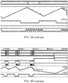
- Fig. 1A shows an example of an operation 100 of a transponder.
- a command is received by the transponder, it should be decoded, processed and a response should be transmitted back to the reader.
- a voltage sensor based mechanism can be used to gate clocks of most of the active digital logic momentarily to reduce power consumption and resume on voltage recovery. This is useful to avoid resets due to low voltage, particularly at lower field strengths. This is referred to as a clock-stop concept.
- the clock-stop concept or clock-stop feature enables achieving a higher distance of operation of the transponder from the reader (i.e.
- vdda_int denotes an internal signal that represents the operating voltage of the transponder.
- Fig. 1B shows another example of an operation 102 of a transponder.
- a reader communicates to a transponder a specific sequence of logical bits 0/1, which are amplitude modulated by the reader.
- This amplitude modulation of a created radio frequency (RF) field is referred to as a Miller pause in said technical standard ISO/IEC14443-2.
- RF radio frequency
- the transponder's digital logic (CPU subsystem) remains ungated after the Miller pause, in order to store (i.e. process) one or more bytes of the received command frame in a transponder memory.
- CPU subsystem the transponder's digital logic
- the demodulator of the tag may detect such a drop of voltage as a Miller pause. This, in turn, may result in a wrong Miller decoding and not responding to the command. This may predominantly be visible for higher baud rates such as 212 kbps, 424 kbps and 848 kbps, due to a lower demodulator sensitivity to detect lower Miller pause depths (for example modulation depths of 40%).
- Fig. 1B shows a simulation waveform with a command being received by the transponder ( dmod_sync ).
- the digital processing starts and consumes power causing a voltage drop ( vdda_int ).
- a traditional voltage sensor based clock-stop ( vsens_clkstop_a_o ) is triggered after reaching a threshold voltage (1.8V). This clock-stop ( vsens_clkstop_a_o ) gates the digital processing until the voltage is recovered ( vdda_int ).
- a first problem is that the variation in voltage ( vdda_int ) between Miller pauses may be detected by the demodulator of the transponder as a wrong Miller pause.
- a second problem is that the starting voltage ( vdda_int ) at the start of the next Miller pause may drop due to the digital processing until the start of the next Miller pause; this may result in a higher minimum operating field strength (H min ) as it can trigger a low voltage reset (for example a 1.2V reset in the present example).
- a transponder transmits a response back to the reader.
- the transponder's digital logic copies response bytes to a transmit buffer of said transponder. Since this copying may involve an activity of the central processing unit (CPU), power drops may occur, which may become visible as noise to the reader during response detection. Generally speaking, any activity of the CPU may become visible as noise to the reader during response detection. Readers often employ a signal-to-noise ratio (SNR), and the noise generated as a result of systematic processing by the CPU may be significantly visible. This, in turn, may result in errors in the response detection by the reader, depending on the reader's response detection sensitivity.
- SNR signal-to-noise ratio
- a transponder comprising digital logic for processing one or more portions of a data frame, a status detection unit configured to detect a status of a data frame reception or data frame transmission, and a clock gating unit configured to apply clock gating to said digital logic in dependence on the status of said data frame reception or data frame transmission.
- a response frame can be avoided or at least significantly reduced.
- said portions of the data frame may be bytes of the data frame.
- other portions of the data frame may also be processed by the digital logic, and the presently disclosed status-dependent clock gating may be applied equally well to digital logic that processes other portions than bytes (e.g., portions comprising any number of bits).
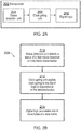
- Fig. 2A shows an illustrative embodiment of a transponder 200.
- the transponder 200 comprises digital logic 202, a status detection unit 204, and a clock gating unit 206.
- the digital logic 202 is configured to process one or more bytes of a data frame.
- the status detection unit 204 is configured to detect a status of a data frame reception or data frame transmission.
- the clock gating unit 206 is configured to apply clock gating to the digital logic 202 in dependence on the status of the data frame reception or in dependence on the status of the data frame transmission.
- Clock gating refers to stalling the clock to the digital logic and/or to preventing the system clock signal from reaching the digital logic.
- Fig. 2B shows an illustrative embodiment of a method 208 of operating a transponder.
- the method 208 comprises, at 210, that the status detection unit 204 detects a status of a data frame reception or data frame transmission, at 212, that the clock gating unit 206 applies clock gating to the digital logic 202 in dependence on the detected status, and at 214, that the digital logic 202 processes one or more bytes of a data frame.
- detecting the status of data frame reception comprises detecting an end of a Miller pause, and the clock gating unit is configured to apply said clock gating after said Miller pause.
- a transponder is set to reception status to receive one or more bytes of a data frame (a command from the reader), because it cannot transmit without a command from a reader.
- An analog demodulator detects Miller pauses and converts the Miller pauses to digital signals, which are used for detecting logic bits 0's and 1's. A transition of such a digital signal from high to low can be regarded as the end of a Miller pause. The same digital signal may be used to gate the digital logic, because the transponder has low power or no power during Miller pause.
- the clock gating unit is configured to apply clock gating after the Miller pause.
- the digital logic is generally active to copy the byte(s) from a receive buffer to internal memory or to execute any other operations.
- the clock gating By applying the clock gating, the power consumed by the digital logic is effectively controlled. In this way, the likelihood of a significant variation in voltage after a Miller pause may be reduced, which in turn reduces the risk that such a voltage variation is detected as a wrong Miller pause by the demodulator. Furthermore, the likelihood of a significant voltage drop at the start of the next Miller pause may also be reduced, so that the minimum operating field strength does not increase to an unacceptable level.
- detecting the status of data frame transmission comprises detecting that the digital logic is active during the transmission of a response, wherein the clock gating unit is configured to apply said clock gating while the digital logic is active.
- detecting that the digital logic is active comprises detecting that the digital logic is copying response data to a transmission buffer.
- a transponder performs, once a command is received, its specific operations and prepares response data for transmission by setting the transponder status to transmission.
- the response data may for example comprise response bytes.
- a CPU subsystem is generally active to copy response data byte(s), one after the other, from internal memory to the transmit buffer or to execute any other operations.
- the clock gating unit is configured to apply clock gating while the digital logic is active during the transmission of a response. In this way, the likelihood that power drops occur during response transmissions may be reduced, which in turn reduces the risk of errors in the response detection by the reader.
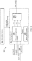
- Fig. 3 shows an illustrative embodiment of a clock gating subsystem 300 of a transponder.
- the clock gating subsystem 300 comprises a clock gating unit 302, a non-volatile memory 310, and a synchronizer 312.
- the clock gating unit 302 comprises a clock_control generator 304, a multiplexer 306, and an active duration counter 308.
- a transponder's demodulator may be sensitive to the drop or rise of the voltage between the Miller pauses of a command.
- a capacitor is often used as a secondary power source, in addition to the power harvested from the field, which may cause the drop or rise of the voltage.
- the drop or rise in the voltage may be regulated by gating the digital logic clocks with a predefined clock during reception.
- the clock control may be optimized so as to regulate the voltage between Miller pauses and to ensure a safe capture of the command by providing a sufficient number of active clocks to perform a copy operation or to perform other digital operations.
- the voltage regulator logic may be configured via the non-volatile memory 310. The use of the non-volatile memory 310 results in effective and practical implementation of the clock gating mechanism.
- the clock_control generator 304 may retrieve clock control configuration settings (i.e. parameters) from said non-volatile memory 310.
- the active duration of the clock control may also be a configuration setting or parameter stored in the non-volatile memory 310.
- the active duration may be defined as the number of clock cycles during which the configured gated clock control is active from the end of a Miller pause. After the active duration, the clock to the digital logic is gated until the next Miller pause.
- the synchronizer 312 is configured to synchronize an asynchronous demodulated signal with the digital logic clock domain.
- the clock_control generator 304 is configured to generate different clock control signals, in dependence on the configuration settings.
- the configuration settings or parameters may be as follows:
- a 2-bit counter may be used to generate these signals. This module may be enabled during command reception ( rx_enable ) .
- the active duration counter 308 maybe a 5-bit counter, which is used to enable the clock_control generator 304 for a configured active duration cycle count (e.g. stored as parameter act_duration in the non-volatile memory 310). If the parameter act_duration is set to 0, then this is treated as a disablement of the active duration feature.
- the multiplexer 306 is configured to multiplex the three types of clock-gating signals based on the configuration settings.
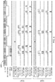
- Fig. 4 shows an illustrative embodiment of the use 400 of different programmable parameters.
- the active duration may be a programmable parameter ( act_duration ) stored in the non-volatile memory 310.
- act_duration has the value 00: this means that the feature to limit the number of active duration clocks after the Miller pause ( dmod ) has been disabled. In other words, it means that the configured clock gating is applied until the next Miller pause.
- the parameter act_duration has the value 04: this means that the feature to limit the number of active duration clocks after the Miller pause ( dmod ) has been enabled and has been set to four.
- the configured clock gating is applied during four cycles after the end of Miller pause, and subsequently the clock is gated until the next Miller pause.
- the clock gating unit 304 is further configured to apply a configured clock gating for a predefined maximum number of clock cycles.
- the configured clock gating comprises disabling the digital logic during a first predefined number of clock cycles and enabling the digital logic during a second predefined number of clock cycles.
- the first predefined number and the second predefined number may for example be 1 and 1, 2 and 2, respectively 3 and 1, as described above.
- the second problem shown in Fig. 1B may be avoided.
- the active duration is disabled, there might be active clocks until the next Miller pause, which might result in a voltage drop at the start of next Miller pause.
- the active clocks encroach the next Miller pause.
- the voltage may be fully recovered before the next Miller pause.
- Fig. 5 shows a simulation result 500 with applied clock gating.
- Fig. 5 shows a simulation waveform for a command that is being received by a transponder ( dmod_sync ).
- the clock-control (E) starts and the digital processing is stalled for predefined intervals to regulate the power or voltage ( vdda_int ).
- the variation in voltage ( vdda_int ) between Miller pauses is well regulated (not dropping below 1.8V) and also the digital processing is completed ahead of the next Miller pause.
- the starting voltage ( vdda_int ) at the start of the next Miller pause is at full strength as the digital processing is completed before the next Miller pause. This may result in a lower minimum operating field strength (H min ) as it may avoid triggering a low voltage reset.
Landscapes
- Engineering & Computer Science (AREA)
- Theoretical Computer Science (AREA)
- Physics & Mathematics (AREA)
- General Physics & Mathematics (AREA)
- General Engineering & Computer Science (AREA)
- Computer Networks & Wireless Communication (AREA)
- Computer Hardware Design (AREA)
- Microelectronics & Electronic Packaging (AREA)
- Artificial Intelligence (AREA)
- Computer Vision & Pattern Recognition (AREA)
- Near-Field Transmission Systems (AREA)
Claims (12)
- Transponder (200), der Folgendes umfasst:eine Digitallogik (202) zum Verarbeiten eines oder mehrerer Teile eines Datenrahmens;eine Statuserkennungseinheit (204), die konfiguriert ist, um einen Datenrahmenempfangs- oder Datenrahmenübertragungsstatus zu erkennen;eine Clock-Gating-Einheit (206), die konfiguriert ist, um ein Clock-Gating in Abhängigkeit vom Datenrahmenempfangs- oder Datenrahmenübertragungsstatus auf die Digitallogik (202) anzuwenden, wobei das Clock-Gating umfasst, dass ein Takt der Digitallogik angehalten wird und/oder dass verhindert wird, dass ein Systemtaktsignal die Digitallogik erreicht;dadurch gekennzeichnet, dass der Transponder (200) ferner einen Analog-Demodulator umfasst, der konfiguriert ist, um eine Miller-Pause zu erkennen und die Miller-Pause in ein Digitalsignal umzuwandeln, wobei eine Miller-Pause ein Zeitintervall ist, in dem ein logisches Bit durch eine Leseeinrichtung amplitudenmoduliert wird;wobei das Erkennen des Datenrahmenempfangsstatus umfasst, dass ein Ende der Miller-Pause durch Erkennen eines Übergangs des Digitalsignals erkannt wird;und wobei die Clock-Gating-Einheit (206) konfiguriert ist, um das Clock-Gating nach der Miller-Pause anzuwenden.
- Transponder (200) nach dem vorhergehenden Anspruch, wobei das Erkennen des Datenrahmenübertragungsstatus umfasst, dass erkannt wird, dass die Digitallogik (202) während der Übertragung einer Antwort aktiv ist, und wobei die Clock-Gating-Einheit (206) konfiguriert ist, um das Clock-Gating anzuwenden, während die Digitallogik (202) aktiv ist, wobei das Erkennen, dass die Digitallogik (202) aktiv ist, umfasst, dass erkannt wird, dass die Digitallogik (202) aktiv ist, um Antwortdaten in einen Sendepuffer zu kopieren.
- Transponder (200) nach einem vorhergehenden Anspruch, wobei das Anwenden des Clock-Gatings eine Ausschaltung der Digitallogik (202) während einer ersten vordefinierten Anzahl von Taktzyklen und eine Einschaltung der Digitallogik (202) während einer zweiten vordefinierten Anzahl von Taktzyklen umfasst.
- Transponder (200) nach Anspruch 3, wobei:die erste vordefinierte Anzahl eins ist und die zweite vordefinierte Anzahl eins ist;die erste vordefinierte Anzahl zwei ist und die zweite vordefinierte Anzahl zwei ist; oderdie erste vordefinierte Anzahl drei ist und die zweite vordefinierte Anzahl eins ist.
- Transponder (200) nach Anspruch 3 oder 4, wobei das Ausschalten der Digitallogik (202) und das Einschalten der Digitallogik (202) wiederholt werden.
- Transponder (200) nach einem der Ansprüche 3 bis 5, wobei die Clock-Gating-Einheit (206) ferner konfiguriert ist, um das Einschalten und Ausschalten für die Dauer einer vordefinierten maximalen Anzahl von Taktzyklen anzuwenden.
- Transponder (200) nach einem der Ansprüche 3 bis 6, wobei die erste vordefinierte Anzahl von Taktzyklen, die zweite vordefinierte Anzahl von Taktzyklen und/oder die vordefinierte maximale Anzahl von Taktzyklen programmierbare Parameter sind.
- Transponder (200) nach Anspruch 7, der ferner einen Speicher zum Speichern der programmierbaren Parameter umfasst.
- Transponder (200) nach Anspruch 8, wobei der Speicher ein nichtflüchtiger Speicher ist.
- Verfahren (208) zum Betreiben eines Transponders (200), wobei das Verfahren Folgendes umfasst:Erkennen (210) eines Datenrahmenempfangs- oder Datenrahmenübertragungsstatus durch eine Statuserkennungseinheit (204) des Transponders (200) ;Anwenden (212) eines Clock-Gatings durch eine Clock-Gating-Einheit (206) des Transponders (200) auf eine Digitallogik (202) des Transponders (200) in Abhängigkeit vom Datenrahmenempfangs- oder Datenrahmenübertragungsstatus, wobei das Clock-Gating umfasst, dass ein Takt der Digitallogik angehalten wird und/oder dass verhindert wird, dass ein Systemtaktsignal die Digitallogik erreicht;Verarbeiten (214) eines oder mehrerer Teile eines Datenrahmens durch die Digitallogik (202);dadurch gekennzeichnet, dass das Verfahren (208) ferner Folgendes umfasst:Erkennen einer Miller-Pause durch einen Analog-Demodulator des Transponders (200) und Umwandeln der Miller-Pause in ein Digitalsignal durch den Analog-Demodulator, wobei eine Miller-Pause ein Zeitintervall ist, in dem ein logisches Bit durch eine Leseeinrichtung amplitudenmoduliert wird;wobei das Erkennen (210) des Datenrahmenempfangsstatus umfasst, dass ein Ende der Miller-Pause durch Erkennen eines Übergangs des Digitalsignals erkannt wird;und wobei die Clock-Gating-Einheit (206) das Clock-Gating nach der Miller-Pause anwendet.
- Computerprogramm, das Befehle umfasst, durch die, wenn sie durch eine Verarbeitungseinheit laufen gelassen werden, das Verfahren (208) nach Anspruch 10 durchgeführt wird.
- Nichttransientes, computerlesbares Medium, das das Computerprogramm nach Anspruch 11 umfasst.
Priority Applications (2)
| Application Number | Priority Date | Filing Date | Title |
|---|---|---|---|
| EP18173666.1A EP3572968B1 (de) | 2018-05-22 | 2018-05-22 | Clock-gating-einheit für einen transponder |
| US16/406,083 US11068040B2 (en) | 2018-05-22 | 2019-05-08 | Clock gating unit for a transponder |
Applications Claiming Priority (1)
| Application Number | Priority Date | Filing Date | Title |
|---|---|---|---|
| EP18173666.1A EP3572968B1 (de) | 2018-05-22 | 2018-05-22 | Clock-gating-einheit für einen transponder |
Publications (2)
| Publication Number | Publication Date |
|---|---|
| EP3572968A1 EP3572968A1 (de) | 2019-11-27 |
| EP3572968B1 true EP3572968B1 (de) | 2021-08-04 |
Family
ID=62244305
Family Applications (1)
| Application Number | Title | Priority Date | Filing Date |
|---|---|---|---|
| EP18173666.1A Active EP3572968B1 (de) | 2018-05-22 | 2018-05-22 | Clock-gating-einheit für einen transponder |
Country Status (2)
| Country | Link |
|---|---|
| US (1) | US11068040B2 (de) |
| EP (1) | EP3572968B1 (de) |
Families Citing this family (1)
| Publication number | Priority date | Publication date | Assignee | Title |
|---|---|---|---|---|
| US11209891B2 (en) | 2019-11-27 | 2021-12-28 | Robert Bosch Gmbh | Clock control to increase robustness of a serial bus interface |
Family Cites Families (16)
| Publication number | Priority date | Publication date | Assignee | Title |
|---|---|---|---|---|
| US5504485A (en) | 1994-07-21 | 1996-04-02 | Amtech Corporation | System for preventing reading of undesired RF signals |
| DE19732643A1 (de) * | 1997-07-29 | 1999-02-04 | Siemens Ag | Schaltungsanordnung zum manipuliergeschützten Empfangen eines OOK-modulierten Signals |
| DE69914692T2 (de) * | 1998-03-27 | 2004-10-21 | Koninkl Philips Electronics Nv | Schaltung für datenträger zum reduzieren von stromverbrauch |
| FR2812142A1 (fr) * | 2000-07-21 | 2002-01-25 | Microcid Sa | Transpondeur passif et lecteur pour une identification sans contact de tels transpondeurs |
| KR100684172B1 (ko) * | 2004-11-24 | 2007-02-20 | 한국전자통신연구원 | Rfid 태그의 저전력 디지털 회로부 |
| US20070297214A1 (en) * | 2006-06-09 | 2007-12-27 | Semiconductor Energy Laboratory Co., Ltd. | Semiconductor device |
| ATE483208T1 (de) * | 2007-04-26 | 2010-10-15 | Em Microelectronic Marin Sa | Transponderschaltung mit doppelter taktableitungseinheit |
| US9064196B1 (en) | 2008-03-13 | 2015-06-23 | Impinj, Inc. | RFID tag dynamically adjusting clock frequency |
| US8193912B1 (en) | 2008-03-13 | 2012-06-05 | Impinj, Inc. | RFID tag dynamically adjusting clock frequency |
| US7605612B1 (en) * | 2008-05-16 | 2009-10-20 | International Business Machines Corporation | Techniques for reducing power requirements of an integrated circuit |
| KR101543646B1 (ko) * | 2009-03-13 | 2015-08-12 | 삼성전자주식회사 | Type-a 복조 장치 및 이를 구비한 집적회로 카드 |
| US8076970B2 (en) * | 2009-06-10 | 2011-12-13 | Infineon Technologies Ag | Adaptive demodulator |
| EP2439678B1 (de) * | 2010-10-05 | 2013-05-01 | Nxp B.V. | Chipkarte |
| JP2016513315A (ja) * | 2013-02-07 | 2016-05-12 | ニューポート、デジタル、テクノロジーズ、オーストラリア、プロプライエタリー、リミテッドNewport Digital Technologies Australia Pty Ltd | Rfid追跡における改善 |
| TWI663820B (zh) * | 2013-08-21 | 2019-06-21 | 日商半導體能源研究所股份有限公司 | 電荷泵電路以及具備電荷泵電路的半導體裝置 |
| CN104636691A (zh) * | 2013-11-13 | 2015-05-20 | 成都新方洲信息技术有限公司 | 一种用rfid系统的应答器 |
-
2018
- 2018-05-22 EP EP18173666.1A patent/EP3572968B1/de active Active
-
2019
- 2019-05-08 US US16/406,083 patent/US11068040B2/en active Active
Non-Patent Citations (1)
| Title |
|---|
| None * |
Also Published As
| Publication number | Publication date |
|---|---|
| US11068040B2 (en) | 2021-07-20 |
| EP3572968A1 (de) | 2019-11-27 |
| US20190361514A1 (en) | 2019-11-28 |
Similar Documents
| Publication | Publication Date | Title |
|---|---|---|
| US8390433B2 (en) | Method and system for low cost, power efficient, wireless transponder devices with enhanced functionality | |
| US20060022798A1 (en) | Reader/writer for transmitting command to IC tag, communication method and communication system based thereon | |
| US5519729A (en) | Method of and device for transmitting serial data structures in systems for identifying information carriers | |
| US6891475B2 (en) | Low-power passive transponder | |
| EP4235501A2 (de) | Leistungsverwaltung | |
| US8015428B2 (en) | Processing device and clock control method | |
| KR20160015193A (ko) | Rfid 트래킹의 개선 | |
| US10599965B2 (en) | RF tag circuit | |
| JP5355092B2 (ja) | クロックフリー起動回路 | |
| JP2009506620A (ja) | データストリーム信号の評価用rfidリーダ及び評価方法 | |
| EP2958056B1 (de) | Funkfrequenztransponderschaltung | |
| US11533081B2 (en) | NFC device detection | |
| KR100450765B1 (ko) | 무선통신매체 및 그 동작방법 | |
| US7429913B2 (en) | Low power digital circuit for RFID tag | |
| CN107580711B (zh) | Rfid应答器、rfid应答器装置和用于rfid应答器与读取设备之间的通信的方法 | |
| EP3572968B1 (de) | Clock-gating-einheit für einen transponder | |
| EP2930647B1 (de) | Kontaktlose Kommunikationsvorrichtung mit Empfängereingangsspannungsstabilisierung | |
| CN105005751B (zh) | 一种rfid标签芯片信号反射方法 | |
| US8076970B2 (en) | Adaptive demodulator | |
| US8195100B2 (en) | Transponder circuit with double clock extractor unit | |
| JP2005151033A (ja) | Rfid通信におけるvpm変調方式 | |
| JP4913465B2 (ja) | Icタグ、icタグシステムおよびそのデータの通信方法 | |
| US20240330613A1 (en) | Reception circuit and smart card including the same | |
| JP2005151075A (ja) | Rfid通信におけるパルスギャップ信号による非同期通信方式 | |
| Jiayin et al. | A novel baseband-processor for LF RFID tag |
Legal Events
| Date | Code | Title | Description |
|---|---|---|---|
| PUAI | Public reference made under article 153(3) epc to a published international application that has entered the european phase |
Free format text: ORIGINAL CODE: 0009012 |
|
| STAA | Information on the status of an ep patent application or granted ep patent |
Free format text: STATUS: THE APPLICATION HAS BEEN PUBLISHED |
|
| AK | Designated contracting states |
Kind code of ref document: A1 Designated state(s): AL AT BE BG CH CY CZ DE DK EE ES FI FR GB GR HR HU IE IS IT LI LT LU LV MC MK MT NL NO PL PT RO RS SE SI SK SM TR |
|
| AX | Request for extension of the european patent |
Extension state: BA ME |
|
| STAA | Information on the status of an ep patent application or granted ep patent |
Free format text: STATUS: REQUEST FOR EXAMINATION WAS MADE |
|
| 17P | Request for examination filed |
Effective date: 20200527 |
|
| RBV | Designated contracting states (corrected) |
Designated state(s): AL AT BE BG CH CY CZ DE DK EE ES FI FR GB GR HR HU IE IS IT LI LT LU LV MC MK MT NL NO PL PT RO RS SE SI SK SM TR |
|
| STAA | Information on the status of an ep patent application or granted ep patent |
Free format text: STATUS: EXAMINATION IS IN PROGRESS |
|
| 17Q | First examination report despatched |
Effective date: 20200710 |
|
| STAA | Information on the status of an ep patent application or granted ep patent |
Free format text: STATUS: EXAMINATION IS IN PROGRESS |
|
| GRAP | Despatch of communication of intention to grant a patent |
Free format text: ORIGINAL CODE: EPIDOSNIGR1 |
|
| STAA | Information on the status of an ep patent application or granted ep patent |
Free format text: STATUS: GRANT OF PATENT IS INTENDED |
|
| INTG | Intention to grant announced |
Effective date: 20210512 |
|
| GRAS | Grant fee paid |
Free format text: ORIGINAL CODE: EPIDOSNIGR3 |
|
| GRAA | (expected) grant |
Free format text: ORIGINAL CODE: 0009210 |
|
| STAA | Information on the status of an ep patent application or granted ep patent |
Free format text: STATUS: THE PATENT HAS BEEN GRANTED |
|
| AK | Designated contracting states |
Kind code of ref document: B1 Designated state(s): AL AT BE BG CH CY CZ DE DK EE ES FI FR GB GR HR HU IE IS IT LI LT LU LV MC MK MT NL NO PL PT RO RS SE SI SK SM TR |
|
| REG | Reference to a national code |
Ref country code: GB Ref legal event code: FG4D |
|
| REG | Reference to a national code |
Ref country code: AT Ref legal event code: REF Ref document number: 1417743 Country of ref document: AT Kind code of ref document: T Effective date: 20210815 |
|
| REG | Reference to a national code |
Ref country code: CH Ref legal event code: EP |
|
| REG | Reference to a national code |
Ref country code: DE Ref legal event code: R096 Ref document number: 602018021049 Country of ref document: DE |
|
| REG | Reference to a national code |
Ref country code: IE Ref legal event code: FG4D |
|
| REG | Reference to a national code |
Ref country code: LT Ref legal event code: MG9D |
|
| REG | Reference to a national code |
Ref country code: NL Ref legal event code: MP Effective date: 20210804 |
|
| REG | Reference to a national code |
Ref country code: AT Ref legal event code: MK05 Ref document number: 1417743 Country of ref document: AT Kind code of ref document: T Effective date: 20210804 |
|
| PG25 | Lapsed in a contracting state [announced via postgrant information from national office to epo] |
Ref country code: RS Free format text: LAPSE BECAUSE OF FAILURE TO SUBMIT A TRANSLATION OF THE DESCRIPTION OR TO PAY THE FEE WITHIN THE PRESCRIBED TIME-LIMIT Effective date: 20210804 Ref country code: SE Free format text: LAPSE BECAUSE OF FAILURE TO SUBMIT A TRANSLATION OF THE DESCRIPTION OR TO PAY THE FEE WITHIN THE PRESCRIBED TIME-LIMIT Effective date: 20210804 Ref country code: FI Free format text: LAPSE BECAUSE OF FAILURE TO SUBMIT A TRANSLATION OF THE DESCRIPTION OR TO PAY THE FEE WITHIN THE PRESCRIBED TIME-LIMIT Effective date: 20210804 Ref country code: ES Free format text: LAPSE BECAUSE OF FAILURE TO SUBMIT A TRANSLATION OF THE DESCRIPTION OR TO PAY THE FEE WITHIN THE PRESCRIBED TIME-LIMIT Effective date: 20210804 Ref country code: HR Free format text: LAPSE BECAUSE OF FAILURE TO SUBMIT A TRANSLATION OF THE DESCRIPTION OR TO PAY THE FEE WITHIN THE PRESCRIBED TIME-LIMIT Effective date: 20210804 Ref country code: NO Free format text: LAPSE BECAUSE OF FAILURE TO SUBMIT A TRANSLATION OF THE DESCRIPTION OR TO PAY THE FEE WITHIN THE PRESCRIBED TIME-LIMIT Effective date: 20211104 Ref country code: PT Free format text: LAPSE BECAUSE OF FAILURE TO SUBMIT A TRANSLATION OF THE DESCRIPTION OR TO PAY THE FEE WITHIN THE PRESCRIBED TIME-LIMIT Effective date: 20211206 Ref country code: AT Free format text: LAPSE BECAUSE OF FAILURE TO SUBMIT A TRANSLATION OF THE DESCRIPTION OR TO PAY THE FEE WITHIN THE PRESCRIBED TIME-LIMIT Effective date: 20210804 Ref country code: BG Free format text: LAPSE BECAUSE OF FAILURE TO SUBMIT A TRANSLATION OF THE DESCRIPTION OR TO PAY THE FEE WITHIN THE PRESCRIBED TIME-LIMIT Effective date: 20211104 Ref country code: LT Free format text: LAPSE BECAUSE OF FAILURE TO SUBMIT A TRANSLATION OF THE DESCRIPTION OR TO PAY THE FEE WITHIN THE PRESCRIBED TIME-LIMIT Effective date: 20210804 |
|
| PG25 | Lapsed in a contracting state [announced via postgrant information from national office to epo] |
Ref country code: PL Free format text: LAPSE BECAUSE OF FAILURE TO SUBMIT A TRANSLATION OF THE DESCRIPTION OR TO PAY THE FEE WITHIN THE PRESCRIBED TIME-LIMIT Effective date: 20210804 Ref country code: LV Free format text: LAPSE BECAUSE OF FAILURE TO SUBMIT A TRANSLATION OF THE DESCRIPTION OR TO PAY THE FEE WITHIN THE PRESCRIBED TIME-LIMIT Effective date: 20210804 Ref country code: GR Free format text: LAPSE BECAUSE OF FAILURE TO SUBMIT A TRANSLATION OF THE DESCRIPTION OR TO PAY THE FEE WITHIN THE PRESCRIBED TIME-LIMIT Effective date: 20211105 |
|
| PG25 | Lapsed in a contracting state [announced via postgrant information from national office to epo] |
Ref country code: NL Free format text: LAPSE BECAUSE OF FAILURE TO SUBMIT A TRANSLATION OF THE DESCRIPTION OR TO PAY THE FEE WITHIN THE PRESCRIBED TIME-LIMIT Effective date: 20210804 |
|
| PG25 | Lapsed in a contracting state [announced via postgrant information from national office to epo] |
Ref country code: DK Free format text: LAPSE BECAUSE OF FAILURE TO SUBMIT A TRANSLATION OF THE DESCRIPTION OR TO PAY THE FEE WITHIN THE PRESCRIBED TIME-LIMIT Effective date: 20210804 |
|
| REG | Reference to a national code |
Ref country code: DE Ref legal event code: R097 Ref document number: 602018021049 Country of ref document: DE |
|
| PG25 | Lapsed in a contracting state [announced via postgrant information from national office to epo] |
Ref country code: SM Free format text: LAPSE BECAUSE OF FAILURE TO SUBMIT A TRANSLATION OF THE DESCRIPTION OR TO PAY THE FEE WITHIN THE PRESCRIBED TIME-LIMIT Effective date: 20210804 Ref country code: SK Free format text: LAPSE BECAUSE OF FAILURE TO SUBMIT A TRANSLATION OF THE DESCRIPTION OR TO PAY THE FEE WITHIN THE PRESCRIBED TIME-LIMIT Effective date: 20210804 Ref country code: RO Free format text: LAPSE BECAUSE OF FAILURE TO SUBMIT A TRANSLATION OF THE DESCRIPTION OR TO PAY THE FEE WITHIN THE PRESCRIBED TIME-LIMIT Effective date: 20210804 Ref country code: EE Free format text: LAPSE BECAUSE OF FAILURE TO SUBMIT A TRANSLATION OF THE DESCRIPTION OR TO PAY THE FEE WITHIN THE PRESCRIBED TIME-LIMIT Effective date: 20210804 Ref country code: CZ Free format text: LAPSE BECAUSE OF FAILURE TO SUBMIT A TRANSLATION OF THE DESCRIPTION OR TO PAY THE FEE WITHIN THE PRESCRIBED TIME-LIMIT Effective date: 20210804 Ref country code: AL Free format text: LAPSE BECAUSE OF FAILURE TO SUBMIT A TRANSLATION OF THE DESCRIPTION OR TO PAY THE FEE WITHIN THE PRESCRIBED TIME-LIMIT Effective date: 20210804 |
|
| PLBE | No opposition filed within time limit |
Free format text: ORIGINAL CODE: 0009261 |
|
| STAA | Information on the status of an ep patent application or granted ep patent |
Free format text: STATUS: NO OPPOSITION FILED WITHIN TIME LIMIT |
|
| 26N | No opposition filed |
Effective date: 20220506 |
|
| PG25 | Lapsed in a contracting state [announced via postgrant information from national office to epo] |
Ref country code: IT Free format text: LAPSE BECAUSE OF FAILURE TO SUBMIT A TRANSLATION OF THE DESCRIPTION OR TO PAY THE FEE WITHIN THE PRESCRIBED TIME-LIMIT Effective date: 20210804 |
|
| PG25 | Lapsed in a contracting state [announced via postgrant information from national office to epo] |
Ref country code: SI Free format text: LAPSE BECAUSE OF FAILURE TO SUBMIT A TRANSLATION OF THE DESCRIPTION OR TO PAY THE FEE WITHIN THE PRESCRIBED TIME-LIMIT Effective date: 20210804 |
|
| REG | Reference to a national code |
Ref country code: CH Ref legal event code: PL |
|
| REG | Reference to a national code |
Ref country code: BE Ref legal event code: MM Effective date: 20220531 |
|
| GBPC | Gb: european patent ceased through non-payment of renewal fee |
Effective date: 20220522 |
|
| PG25 | Lapsed in a contracting state [announced via postgrant information from national office to epo] |
Ref country code: MC Free format text: LAPSE BECAUSE OF FAILURE TO SUBMIT A TRANSLATION OF THE DESCRIPTION OR TO PAY THE FEE WITHIN THE PRESCRIBED TIME-LIMIT Effective date: 20210804 Ref country code: LU Free format text: LAPSE BECAUSE OF NON-PAYMENT OF DUE FEES Effective date: 20220522 Ref country code: LI Free format text: LAPSE BECAUSE OF NON-PAYMENT OF DUE FEES Effective date: 20220531 Ref country code: CH Free format text: LAPSE BECAUSE OF NON-PAYMENT OF DUE FEES Effective date: 20220531 |
|
| PG25 | Lapsed in a contracting state [announced via postgrant information from national office to epo] |
Ref country code: IE Free format text: LAPSE BECAUSE OF NON-PAYMENT OF DUE FEES Effective date: 20220522 Ref country code: FR Free format text: LAPSE BECAUSE OF NON-PAYMENT OF DUE FEES Effective date: 20220531 |
|
| PG25 | Lapsed in a contracting state [announced via postgrant information from national office to epo] |
Ref country code: GB Free format text: LAPSE BECAUSE OF NON-PAYMENT OF DUE FEES Effective date: 20220522 Ref country code: BE Free format text: LAPSE BECAUSE OF NON-PAYMENT OF DUE FEES Effective date: 20220531 |
|
| P01 | Opt-out of the competence of the unified patent court (upc) registered |
Effective date: 20230725 |
|
| PG25 | Lapsed in a contracting state [announced via postgrant information from national office to epo] |
Ref country code: HU Free format text: LAPSE BECAUSE OF FAILURE TO SUBMIT A TRANSLATION OF THE DESCRIPTION OR TO PAY THE FEE WITHIN THE PRESCRIBED TIME-LIMIT; INVALID AB INITIO Effective date: 20180522 |
|
| PG25 | Lapsed in a contracting state [announced via postgrant information from national office to epo] |
Ref country code: MK Free format text: LAPSE BECAUSE OF FAILURE TO SUBMIT A TRANSLATION OF THE DESCRIPTION OR TO PAY THE FEE WITHIN THE PRESCRIBED TIME-LIMIT Effective date: 20210804 Ref country code: CY Free format text: LAPSE BECAUSE OF FAILURE TO SUBMIT A TRANSLATION OF THE DESCRIPTION OR TO PAY THE FEE WITHIN THE PRESCRIBED TIME-LIMIT Effective date: 20210804 |
|
| PG25 | Lapsed in a contracting state [announced via postgrant information from national office to epo] |
Ref country code: TR Free format text: LAPSE BECAUSE OF FAILURE TO SUBMIT A TRANSLATION OF THE DESCRIPTION OR TO PAY THE FEE WITHIN THE PRESCRIBED TIME-LIMIT Effective date: 20210804 |
|
| PGFP | Annual fee paid to national office [announced via postgrant information from national office to epo] |
Ref country code: DE Payment date: 20240418 Year of fee payment: 7 |
|
| PG25 | Lapsed in a contracting state [announced via postgrant information from national office to epo] |
Ref country code: MT Free format text: LAPSE BECAUSE OF FAILURE TO SUBMIT A TRANSLATION OF THE DESCRIPTION OR TO PAY THE FEE WITHIN THE PRESCRIBED TIME-LIMIT Effective date: 20210804 |