EP3557596A1 - Tape-like contact and method for manufacturing same - Google Patents
Tape-like contact and method for manufacturing same Download PDFInfo
- Publication number
- EP3557596A1 EP3557596A1 EP17883571.6A EP17883571A EP3557596A1 EP 3557596 A1 EP3557596 A1 EP 3557596A1 EP 17883571 A EP17883571 A EP 17883571A EP 3557596 A1 EP3557596 A1 EP 3557596A1
- Authority
- EP
- European Patent Office
- Prior art keywords
- shaped
- tape
- contact
- brazing material
- shaped contact
- Prior art date
- Legal status (The legal status is an assumption and is not a legal conclusion. Google has not performed a legal analysis and makes no representation as to the accuracy of the status listed.)
- Granted
Links
- 238000004519 manufacturing process Methods 0.000 title claims description 30
- 238000000034 method Methods 0.000 title claims description 16
- 239000000463 material Substances 0.000 claims abstract description 319
- 238000005219 brazing Methods 0.000 claims abstract description 174
- 238000009792 diffusion process Methods 0.000 claims abstract description 57
- 229910052751 metal Inorganic materials 0.000 claims abstract description 57
- 239000002184 metal Substances 0.000 claims abstract description 56
- 238000005520 cutting process Methods 0.000 claims abstract description 7
- 229910045601 alloy Inorganic materials 0.000 claims description 31
- 239000000956 alloy Substances 0.000 claims description 31
- 229910017944 Ag—Cu Inorganic materials 0.000 claims description 15
- 238000010438 heat treatment Methods 0.000 claims description 15
- 238000002844 melting Methods 0.000 claims description 10
- 230000008018 melting Effects 0.000 claims description 10
- 229910052802 copper Inorganic materials 0.000 claims description 6
- 229910052759 nickel Inorganic materials 0.000 claims description 6
- 229910052709 silver Inorganic materials 0.000 claims description 5
- 229910052718 tin Inorganic materials 0.000 claims description 5
- 230000005611 electricity Effects 0.000 claims description 4
- 229910052738 indium Inorganic materials 0.000 claims description 4
- 229910052698 phosphorus Inorganic materials 0.000 claims description 3
- 229910052748 manganese Inorganic materials 0.000 claims description 2
- 238000003825 pressing Methods 0.000 claims description 2
- 229910052710 silicon Inorganic materials 0.000 claims description 2
- 229910052725 zinc Inorganic materials 0.000 claims description 2
- 239000000470 constituent Substances 0.000 abstract description 7
- 238000003466 welding Methods 0.000 description 28
- 238000012360 testing method Methods 0.000 description 26
- 230000000052 comparative effect Effects 0.000 description 24
- 239000010949 copper Substances 0.000 description 19
- 206010040844 Skin exfoliation Diseases 0.000 description 13
- 229910000679 solder Inorganic materials 0.000 description 10
- XOLBLPGZBRYERU-UHFFFAOYSA-N SnO2 Inorganic materials O=[Sn]=O XOLBLPGZBRYERU-UHFFFAOYSA-N 0.000 description 7
- 229910001316 Ag alloy Inorganic materials 0.000 description 6
- 230000017525 heat dissipation Effects 0.000 description 5
- PJXISJQVUVHSOJ-UHFFFAOYSA-N indium(III) oxide Inorganic materials [O-2].[O-2].[O-2].[In+3].[In+3] PJXISJQVUVHSOJ-UHFFFAOYSA-N 0.000 description 4
- 239000000203 mixture Substances 0.000 description 4
- PXHVJJICTQNCMI-UHFFFAOYSA-N nickel Substances [Ni] PXHVJJICTQNCMI-UHFFFAOYSA-N 0.000 description 4
- 229910017755 Cu-Sn Inorganic materials 0.000 description 3
- 229910017927 Cu—Sn Inorganic materials 0.000 description 3
- RIRXDDRGHVUXNJ-UHFFFAOYSA-N [Cu].[P] Chemical compound [Cu].[P] RIRXDDRGHVUXNJ-UHFFFAOYSA-N 0.000 description 3
- 238000004458 analytical method Methods 0.000 description 3
- 230000000694 effects Effects 0.000 description 3
- 238000004453 electron probe microanalysis Methods 0.000 description 3
- 239000012535 impurity Substances 0.000 description 3
- 238000005259 measurement Methods 0.000 description 3
- 229910001175 oxide dispersion-strengthened alloy Inorganic materials 0.000 description 3
- 238000012545 processing Methods 0.000 description 3
- 229910017937 Ag-Ni Inorganic materials 0.000 description 2
- 229910017727 AgNi Inorganic materials 0.000 description 2
- 229910017984 Ag—Ni Inorganic materials 0.000 description 2
- 229910000881 Cu alloy Inorganic materials 0.000 description 2
- 229910017888 Cu—P Inorganic materials 0.000 description 2
- BQCADISMDOOEFD-UHFFFAOYSA-N Silver Chemical compound [Ag] BQCADISMDOOEFD-UHFFFAOYSA-N 0.000 description 2
- 230000008021 deposition Effects 0.000 description 2
- 238000013461 design Methods 0.000 description 2
- 230000002349 favourable effect Effects 0.000 description 2
- 230000020169 heat generation Effects 0.000 description 2
- 150000002739 metals Chemical class 0.000 description 2
- 238000005096 rolling process Methods 0.000 description 2
- 239000004332 silver Substances 0.000 description 2
- 238000003892 spreading Methods 0.000 description 2
- 229910001339 C alloy Inorganic materials 0.000 description 1
- RYGMFSIKBFXOCR-UHFFFAOYSA-N Copper Chemical compound [Cu] RYGMFSIKBFXOCR-UHFFFAOYSA-N 0.000 description 1
- 229910000570 Cupronickel Inorganic materials 0.000 description 1
- 229910000990 Ni alloy Inorganic materials 0.000 description 1
- 229910006688 SnO2—In2O3 Inorganic materials 0.000 description 1
- 239000000654 additive Substances 0.000 description 1
- 230000000996 additive effect Effects 0.000 description 1
- 230000015572 biosynthetic process Effects 0.000 description 1
- YOCUPQPZWBBYIX-UHFFFAOYSA-N copper nickel Chemical compound [Ni].[Cu] YOCUPQPZWBBYIX-UHFFFAOYSA-N 0.000 description 1
- KUNSUQLRTQLHQQ-UHFFFAOYSA-N copper tin Chemical compound [Cu].[Sn] KUNSUQLRTQLHQQ-UHFFFAOYSA-N 0.000 description 1
- 230000007547 defect Effects 0.000 description 1
- 230000001687 destabilization Effects 0.000 description 1
- 230000006866 deterioration Effects 0.000 description 1
- 208000037265 diseases, disorders, signs and symptoms Diseases 0.000 description 1
- 239000006185 dispersion Substances 0.000 description 1
- 238000010894 electron beam technology Methods 0.000 description 1
- 239000011261 inert gas Substances 0.000 description 1
- 230000010354 integration Effects 0.000 description 1
- 230000001788 irregular Effects 0.000 description 1
- 230000007774 longterm Effects 0.000 description 1
- 239000007769 metal material Substances 0.000 description 1
- 230000000414 obstructive effect Effects 0.000 description 1
- 238000005457 optimization Methods 0.000 description 1
- 238000004663 powder metallurgy Methods 0.000 description 1
- 230000002265 prevention Effects 0.000 description 1
- 239000010944 silver (metal) Substances 0.000 description 1
- 239000006104 solid solution Substances 0.000 description 1
- 239000011135 tin Substances 0.000 description 1
- 239000011701 zinc Substances 0.000 description 1
Images


Classifications
-
- B—PERFORMING OPERATIONS; TRANSPORTING
- B23—MACHINE TOOLS; METAL-WORKING NOT OTHERWISE PROVIDED FOR
- B23K—SOLDERING OR UNSOLDERING; WELDING; CLADDING OR PLATING BY SOLDERING OR WELDING; CUTTING BY APPLYING HEAT LOCALLY, e.g. FLAME CUTTING; WORKING BY LASER BEAM
- B23K1/00—Soldering, e.g. brazing, or unsoldering
- B23K1/0008—Soldering, e.g. brazing, or unsoldering specially adapted for particular articles or work
-
- H—ELECTRICITY
- H01—ELECTRIC ELEMENTS
- H01R—ELECTRICALLY-CONDUCTIVE CONNECTIONS; STRUCTURAL ASSOCIATIONS OF A PLURALITY OF MUTUALLY-INSULATED ELECTRICAL CONNECTING ELEMENTS; COUPLING DEVICES; CURRENT COLLECTORS
- H01R4/00—Electrically-conductive connections between two or more conductive members in direct contact, i.e. touching one another; Means for effecting or maintaining such contact; Electrically-conductive connections having two or more spaced connecting locations for conductors and using contact members penetrating insulation
- H01R4/58—Electrically-conductive connections between two or more conductive members in direct contact, i.e. touching one another; Means for effecting or maintaining such contact; Electrically-conductive connections having two or more spaced connecting locations for conductors and using contact members penetrating insulation characterised by the form or material of the contacting members
-
- B—PERFORMING OPERATIONS; TRANSPORTING
- B23—MACHINE TOOLS; METAL-WORKING NOT OTHERWISE PROVIDED FOR
- B23K—SOLDERING OR UNSOLDERING; WELDING; CLADDING OR PLATING BY SOLDERING OR WELDING; CUTTING BY APPLYING HEAT LOCALLY, e.g. FLAME CUTTING; WORKING BY LASER BEAM
- B23K3/00—Tools, devices, or special appurtenances for soldering, e.g. brazing, or unsoldering, not specially adapted for particular methods
- B23K3/06—Solder feeding devices; Solder melting pans
- B23K3/0607—Solder feeding devices
- B23K3/0623—Solder feeding devices for shaped solder piece feeding, e.g. preforms, bumps, balls, pellets, droplets
-
- H—ELECTRICITY
- H01—ELECTRIC ELEMENTS
- H01H—ELECTRIC SWITCHES; RELAYS; SELECTORS; EMERGENCY PROTECTIVE DEVICES
- H01H1/00—Contacts
- H01H1/02—Contacts characterised by the material thereof
- H01H1/021—Composite material
- H01H1/023—Composite material having a noble metal as the basic material
- H01H1/0231—Composite material having a noble metal as the basic material provided with a solder layer
-
- H—ELECTRICITY
- H01—ELECTRIC ELEMENTS
- H01H—ELECTRIC SWITCHES; RELAYS; SELECTORS; EMERGENCY PROTECTIVE DEVICES
- H01H1/00—Contacts
- H01H1/06—Contacts characterised by the shape or structure of the contact-making surface, e.g. grooved
-
- H—ELECTRICITY
- H01—ELECTRIC ELEMENTS
- H01H—ELECTRIC SWITCHES; RELAYS; SELECTORS; EMERGENCY PROTECTIVE DEVICES
- H01H11/00—Apparatus or processes specially adapted for the manufacture of electric switches
- H01H11/04—Apparatus or processes specially adapted for the manufacture of electric switches of switch contacts
-
- H—ELECTRICITY
- H01—ELECTRIC ELEMENTS
- H01H—ELECTRIC SWITCHES; RELAYS; SELECTORS; EMERGENCY PROTECTIVE DEVICES
- H01H49/00—Apparatus or processes specially adapted to the manufacture of relays or parts thereof
-
- H—ELECTRICITY
- H01—ELECTRIC ELEMENTS
- H01R—ELECTRICALLY-CONDUCTIVE CONNECTIONS; STRUCTURAL ASSOCIATIONS OF A PLURALITY OF MUTUALLY-INSULATED ELECTRICAL CONNECTING ELEMENTS; COUPLING DEVICES; CURRENT COLLECTORS
- H01R43/00—Apparatus or processes specially adapted for manufacturing, assembling, maintaining, or repairing of line connectors or current collectors or for joining electric conductors
- H01R43/16—Apparatus or processes specially adapted for manufacturing, assembling, maintaining, or repairing of line connectors or current collectors or for joining electric conductors for manufacturing contact members, e.g. by punching and by bending
-
- B—PERFORMING OPERATIONS; TRANSPORTING
- B23—MACHINE TOOLS; METAL-WORKING NOT OTHERWISE PROVIDED FOR
- B23K—SOLDERING OR UNSOLDERING; WELDING; CLADDING OR PLATING BY SOLDERING OR WELDING; CUTTING BY APPLYING HEAT LOCALLY, e.g. FLAME CUTTING; WORKING BY LASER BEAM
- B23K2101/00—Articles made by soldering, welding or cutting
- B23K2101/36—Electric or electronic devices
- B23K2101/38—Conductors
-
- H—ELECTRICITY
- H01—ELECTRIC ELEMENTS
- H01H—ELECTRIC SWITCHES; RELAYS; SELECTORS; EMERGENCY PROTECTIVE DEVICES
- H01H1/00—Contacts
- H01H1/02—Contacts characterised by the material thereof
- H01H1/021—Composite material
- H01H1/023—Composite material having a noble metal as the basic material
-
- H—ELECTRICITY
- H01—ELECTRIC ELEMENTS
- H01H—ELECTRIC SWITCHES; RELAYS; SELECTORS; EMERGENCY PROTECTIVE DEVICES
- H01H50/00—Details of electromagnetic relays
- H01H50/54—Contact arrangements
Definitions
- the present invention relates to a tape-shaped contact member for forming a component of a switching electrical contact of a relay, a switch or the like. Specifically, the present invention relates to a tape-shaped contact member for supplying a chip-shaped contact component that is bonded to a terminal of a switching electrical contact, the tape-shaped contact member being capable of supplying a contact component which hardly suffers from poor contact while adapting to downsizing and height reduction.
- Fig. 8 is a view illustrating a structure of a general relay.
- Fig. 9 is a view illustrating a structure of a relay of flexure type as one aspect of the relay.
- a contact component is bonded to a terminal (electrically conductive plate), and an electrical circuit is electrically switched by the contact component.
- a contact component a chip-shaped contact component to be welded and bonded to a terminal is known.
- Such a contact component is used in both a fixed contact and a movable contact in Figs. 8 and 9 .
- Examples of the chip-shaped contact component include contact components in which a welding material for bonding the contact component to a terminal is bonded to a contact material such as a silver alloy as in Fig. 10 .
- the welding material includes a high-resistance metallic material such as a copper-nickel alloy, and an irregular projection is formed on a bonding surface.
- the contact component is bonded to a terminal by resistance welding using the projection of the welding material.
- a contact component including a contact material and a thin brazing material layer (back solder) as in Fig. 11 is known.
- the contact component including back solder is bonded to a terminal by heating and melting a brazing material.
- a tape-shaped contact member is manufactured, and cut to an arbitrary length to manufacture a chip-shaped contact component, and the contact component is bonded to a terminal.
- a tape-shaped contact member is a long material having the same cross-sectional shape as in Figs. 10 and 11 , and is obtained by bonding to a tape-shaped contact material a tape-shaped welding material subjected to projection processing in advance, or a tape-shaped brazing material subjected to rolling processing in advance.
- the applicant of the present application has developed and disclosed a combination of a projection and a brazing material as described in Patent Document 1.
- Patent Document 1 JP 4279645 B2
- the configuration of a chip-shaped contact component to be used for relays also needs to be improved in light of these requirements.
- the above-mentioned conventional contact components cannot sufficiently meet these requirements. That is, of the above-mentioned contact components, the former contact component including a welding material provided with a convex projection is obstructive to height reduction and downsizing of contact components because of the thickness of the welding material.
- the welding material having a thermal conductivity lower than that of the contact material hinders heat dissipation, and is therefore a source of concern to capacity increase of electrical contacts.
- the welding material has high electric resistance, thus generates a large amount of heat when fed with electricity, and is therefore advantageous for resistance welding, but causes an increase in heat generation when used as a contact material, and is a source of concern to capacity increase of electrical contacts in this regard.
- the latter contact component having back solder is bonded to a terminal with a thin brazing material layer, and therefore can be expected to adapt to height reduction.
- this type of contact component has the problem that at the time of bonding the contact component to a terminal, only a contact end portion is welded, resulting in destabilization of welding to the terminal, or a molten brazing material protrudes, so that the brazing material is deposited on the surface of a contact material or the terminal, resulting in occurrence of contact disorders.
- the contact component having back solder is advantageous from the viewpoint of a bonding force because a contact material can be bonded to a terminal with the entire bonding surface.
- bonding work in a strictly horizontal state is required. It is difficult to achieve the above-mentioned strict design and processing of a brazing material layer and bonding conditions for a contact component that needs to be downsized.
- the contact component in Patent Document 1 by the applicant of the present application takes protrusion of a brazing material, etc. into consideration, but does not necessarily sufficiently meet more advanced requirements for downsizing.
- the present invention has been made against the above-mentioned backgrounds, and provides a tape-shaped contact member for manufacturing a chip-shaped contact component for manufacturing a switching electrical contact, the chip-shaped contact component being capable of adapting to downsizing and height reduction, and having contact performance without suffering from poor bonding to a terminal etc.
- the configuration of such a contact component is clarified.
- a member formed in a chip shape in order to bond the member to a terminal etc. is referred to as a "contact component”
- a tape-shaped material for manufacturing the chip-shaped contact component is referred to as a "contact member”.
- a contact material as a material to which a brazing material is bonded is referred to as a "contact material”.
- the present inventors conducted studies on improvement of the shape of a brazing material while avoiding application of the above-described conventional welding material. As a result, the present inventors decided to apply a protrusive (wire-shaped) brazing material, which is locally elevated on a bonding surface of a contact material, in place of a layered (tape-shaped) brazing material which covers the bonding surface of the contact material. That is, the present inventors decided to form a projection (protrusion) including a brazing material on the bonding surface of the contact material. The present inventors arrived at the present invention by finding that the various problems described above can be solved by optimizing the state of a bonding portion between the projection including a brazing material and the contact material in addition to changing the shape as described above.
- the present invention provides a tape-shaped contact member including a tape-shaped contact material.
- a tape-shaped contact material In the tape-shaped contact material, at least one wire-shaped brazing material is bonded to the tape-shaped contact material, at least one projection including the brazing material and protruding from a surface of the contact material is formed in a cross-sectional shape, a diffusion region containing a metal component forming the brazing material is formed along an interface with the brazing material inside the contact material, and the diffusion region has a thickness of 2 ⁇ m or more and 10 ⁇ m or less.
- a chip-shaped contact component can be obtained by cutting the tape-shaped contact member of the present invention to a desired length.
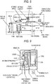
- the cross-sectional shape of the tape-shaped contact member of the present invention is as shown in Fig. 1 , and a projection including a brazing material is formed on a surface of the contact material ( Fig. 1(a) ).
- the chip-shaped contact component obtained from the tape-shaped contact member of the present invention can be bonded to a terminal etc. of an electrical contact by resistance welding, and the chip-shaped contact component is bonded to the terminal when the projection including a brazing material is melted.
- the amount (volume) of the brazing material is limited in comparison with a conventional contact member including a layered brazing material.
- protrusion of the molten brazing material can be effectively suppressed.
- Comparison between the contact component of the present invention and a contact component including a welding material provided with a conventional projection shows that the contact component of the present invention does not contain a welding material, and therefore can contribute to height reduction corresponding to the thickness of the welding material. Further, since there is no welding material, excellent heat dissipation property is exhibited because, so that it is possible to reduce wear of the contact material.
- a moderate bonding area between the contact member and the terminal can be set.
- the brazing material forming a projection and the contact material are bonded to each other while having a predetermined diffusion region. This means that in the present invention, the brazing material and the contact material are moderately integrated with each other.
- the diffusion region on the periphery of the projection and the terminal can be firmly bonded to each other by resistance heat generated in the vicinity of the projection.
- the entire projection is formed of the brazing material, and wet-spreading of the brazing material occurs during bonding.
- the bonding area can be increased.
- a contact component to which a welding material provided with a conventional projection, has a small bonding area because a range over which melting occurs during bonding is limited.
- the contact material can be firmly bonded to the terminal by the effect of increasing the bonding force and optimization of the bonding area in the invention of the present application.
- the heat dissipation effect is enhanced, so that the durability of the contact material that is apt to have a high temperature during operation can be improved.
- the tape-shaped contact member of the present invention has a tape-shaped contact member and a wire-shaped brazing material as basic components.
- the contact material is preferably an Ag-based contact material.
- the Ag-based contact material is a contact material formed of Ag or an Ag alloy. Ag is preferably pure Ag having a purity of 99% by mass or more.
- As the Ag alloy a contact material including Ag containing at least one of Cu, Ni, Zn, Sn and In is preferable. Ag and the Ag alloy may contain inevitable impurities.
- an oxide dispersion strengthened contact material having a phase configuration with two or more phases is applied as well as a solid solution alloy such as an Ag-Cu alloy, or an alloy formed by powder metallurgy, such as an Ag-Ni alloy or an Ag-C alloy.
- the oxide dispersion strengthened contact material is widely used as a contact material for on-vehicle relays, and examples of the oxide dispersion strengthened contact material include Ag-SnO 2 alloys, Ag-SnO 2 -In 2 O 3 alloys, Ag-ZnO alloys and Ag-SnO 2 -Sn 2 Bi 2 O 7 -In 2 O 3 alloys.
- the dimensions of the tape-shaped contact material are not particularly limited.
- the width (i.e. a direction perpendicular to the longitudinal direction of the tape material) and the thickness of the tape-shaped contact material can be freely set according to a use purpose.
- a contact material having a width of 2.0 mm or more and a thickness of 0.4 mm or more is used.
- the brazing material is preferably one formed of an Ag-Cu alloy from the viewpoint of a melting point and a bonding force.
- the brazing material formed of an Ag-Cu alloy include Ag-Cu alloys having an Ag content of 72% by mass or more and 85% by mass or less. It will be preferable if a brazing material including an Ag-Cu alloy further contains at least one of P, Sn, In, Ni, Si and Mn. Specific examples include Ag-P-Cu alloy solder (phosphorus copper solder) and Ag-Cu-Sn alloys (silver solder). These brazing materials are such ones as having a moderate melting point in bonding of the contact material.
- the above-described AgCu alloy that forms a brazing material may contain inevitable impurities.
- the Zn content is controlled. Specifically, a brazing material having a Zn content of 20% by mass or less is preferable. Studies by the present inventors show that when a brazing material containing a relatively large amount of Zn in application of an Ag-based contact material, the brazing material may be easily peeled off because sufficient bonding strength is not obtained. Therefore, a brazing material having an appropriate melting point and containing Zn in an amount of more than 20% by mass is not preferable.
- the Zn content of the brazing material is more preferably 15% by mass or less. When the Zn content is more than 15% by mass and not more than 20% by mass, peeling may occur in the case of, for example, strongly twisting the contact member, and care is often necesssary in handling.
- a wire-shaped brazing material is bonded to a tape-shaped contact material to obtain a contact member. At least one wire-shaped brazing material is necessary, and a plurality of wires (projections) may be bonded. As shown in Fig. 2 , one wire-shaped brazing material can be bonded to the central portion of the contact material, or two wire-shaped brazing materials can be bonded in the vicinity of both end portions.
- the wire diameter of the wire-shaped brazing material to be bonded is preferably about 0.01 times or more and 0.1 times or less of the width of the contact material.
- the wires have the above-mentioned conditions as a whole.
- the tape-shaped contact of the present invention is based on a structure in which a wire-shaped brazing material is directly bonded to a tape-shaped contact material, but it is preferable that an intermediate metal layer for increasing bonding strength between the contact material and the brazing material is formed, the wire-shaped brazing material is bonded to the intermediate metal layer ( Fig. 1(b) ).
- the intermediate metal layer it is preferable to apply an intermediate metal layer formed of a metal to which metal elements (Cu or Ag) from the brazing material are easily diffused.
- the constituent material of the intermediate metal layer is preferably a material containing at least one of Ag, Ni and Cu. Specifically, one of Ag (preferably pure Ag having a purity of 99% by mass or more), an Ag alloy such as an AgNi alloy (preferably an AgNi alloy containing 0.2% by mass or less of Ni and inevitable impurities) and Cu (preferably pure Cu having a purity of 99% by mass or more).
- Ag preferably pure Ag having a purity of 99% by mass or more
- an Ag alloy such as an AgNi alloy (preferably an AgNi alloy containing 0.2% by mass or less of Ni and inevitable impurities)
- Cu preferably pure Cu having a purity of 99% by mass or more.
- the intermediate metal layer prefferably has a thickness of 0.02 mm or more and 0.2 mm or less. This is because the degree of dimensional freedom for the thickness of the contact member can be secured while bonding strength is secured. Even when the intermediate metal layer is applied, one or more wire-shaped brazing materials can be bonded to the intermediate metal layer as in Fig. 2 .
- a diffusion region is formed along an interface with the brazing material inside the contact material or inside the intermediate metal layer.
- the diffusion region is formed by diffusion of the constituent metal of the brazing material to the contact material or the intermediate metal layer.
- an Ag-based contact materia! is applied as a contact material
- a brazing material containing an Ag-Cu alloy (Ag-P-Cu alloy, Ag-Cu-Sn alloy or the like) is applied as a brazing material
- Cu as a metal component of the brazing material is diffused to the diffusion region.
- a region containing Ag of the contact material and Cu of the brazing material is recognized as the diffusion region.
- the diffusion region is not required to have a constant composition, and often has a composition inclined to a distance from the brazing material interface. That is, the diffusion region is discriminated on the basis of whether or not a metal other than the constituent metals of the contact material, which corresponds to the constituent metal of the brazing material, is contained inside the contact material.
- the diffusion region formed as described above is required to have a thickness of 2 ⁇ m or more and 10 ⁇ m or less.
- the thickness is less than 2 ⁇ m, integration of the contact material and the brazing material (projection) is insufficient, and which may cause a risk of a poor bonding in manufacturing an electrical contact.
- the thickness is more than 10 ⁇ m, a change in composition of the brazing material will increase, and which may deteriorate the original performance of the brazing material.
- the diffusion region has an excessively large thickness, there arises such a problem that thermal conductivity is deteriorated.
- the thickness of the diffusion region is strictly set to improve bondability and heat dissipation property in a chip-shaped contact component.
- the thickness of the diffusion region is a thickness (t) between a boundary line between the contact material or intermediate metal layer and the diffusion region and a boundary line between the wire-shaped brazing material and the diffusion region as shown in Fig. 3 .
- the thickness is measured at a plurality of points, and an average value of the measurements is applied.
- the diffusion regions of all the wire-shaped brazing materials are required to have a thickness of 2 ⁇ m or more and 10 ⁇ m or less.
- the width of the bonding interface is more preferably larger than the bonding width of the brazing material by a certain amount or more.
- the bonding width is a direct distance between both end portions of the brazing material brought into contact with and bonded to the contact material as shown in Fig. 3 .
- the bonding width (W) of the brazing material and the diameter (D 1 ) of the brazing material satisfy the relationship of W ⁇ 0.5D 1 .
- W is less than 0.5D 1 , it may be impossible to sufficiently secure the bonding force between the brazing material and the contact material even when heat treatment is performed for formation of a diffusion layer.
- the tape-shaped contact member of the present invention is cut to an appropriate length according to a use purpose of the tape-shaped contact member, and used for manufacturing a contact component, and when the bonding force of the brazing material is insufficient, peeling may occur during cutting. Accordingly, when the brazing material is bonded to the contact material, it is preferable that the brazing material is moderately pressed to be bonded, so that the bonding width is secured, and the diffusion layer is then formed.
- the diameter (D 1 ) of the brazing material can be obtained by measuring the diameter of the cross-section.
- the brazing material may have an elliptic or indefinite shape due to deformation of the brazing material. In this case, it is preferable that a circular shape is assumed on the basis of the circumference length of the cross-section of the brazing material, and the diameter of the circular shape is set to D 1 .
- the upper limit of the bonding width W of the brazing material is preferably equal to or less than 1.7D 1 .
- W is 1.7D 1 or less, a sufficient bonding force is secured.
- w is more than 1.7D 1 , the brazing material (projection) is excessively collapsed, and may fail to effectively function in resistance welding.
- the bonding width (W) of the brazing material and the diameter (D 1 ) of the brazing material satisfy the above-described relationship in all the wire-shaped brazing material bonding portions.
- the tape-shaped contact member of the present invention can be manufactured by bonding a wire-shaped brazing material to a tape-shaped contact material, and then forming a diffusion region in the vicinity of a bonding interface of the wire-shaped brazing material. That is, the method includes the steps of: pressure-bonding at least one wire-shaped brazing material to a tape-shaped contact material; and forming a diffusion region by performing heating at a temperature equal to or higher than 500°C and equal to or lower than the melting point of the brazing material.
- an intermediate metal layer may be formed between the contact material and the brazing material.
- a contact member including an intermediate metal layer a tape-shaped contact material and a tape-shaped intermediate metal layer are bonded to each other, and a wire-shaped brazing material is then pressure-bonded to the intermediate metal layer.
- the tape-shaped intermediate metal layer and the wire-shaped brazing material may be simultaneously pressure-bonded to the tape-shaped contact material.
- the wire-shaped brazing materials may be sequentially or simultaneously bonded.
- specific bonding methods for bonding the wire-shaped brazing material include pressure-bonding by a rolling roll (including a grooved roll).
- a rolling roll including a grooved roll
- the wire-shaped brazing material is bonded by applying pressure until the bonding width W of the wire-shaped brazing material and the diameter D 0 of the wire-shaped brazing material satisfy the relationship of W ⁇ 0.5D 0 .
- W is preferably equal to or less than 1.7D 0 .
- Application of pressure here can be appropriately adjusted according to the materials and dimensions of the contact material, the intermediate metal layer and the brazing material.
- heating is performed at a temperature equal to or higher than 500°C and equal to or lower than the melting point of the brazing material.
- the heat treatment time is preferably 0.25 hours or more and 1.0 hour.
- the heat treatment atmosphere may be an air atmosphere, or an inert gas atmosphere or a reducing atmosphere.
- the above-described tape-shaped contact member of the present invention is appropriately cut to obtain a chip-shaped contact component for manufacturing an electrical contact.
- the chip-shaped contact component may have a length appropriate to the dimensions of an electrical contact to be manufactured and a terminal to be bonded.
- the length of the tape-shaped contact member of the present invention is not limited.
- the contact component can be obtained without cutting the tape-shaped contact member.
- the chip-shaped contact component has at least one projection on the bonding surface to the terminal in a cross-sectional shape.
- the projection is abutted against the terminal to be bonded, and the contact component is fed with electricity and pressed to manufacture the electrical contact.
- the chip-shaped contact component of the present invention is useful for a switching electrical contact, specifically as a constituent material for relays and switches.
- the contact component is fed with electricity while being pressed to the terminal.
- the current is 2 kA to 10 kA
- the pressure is 2 kgf to 10 kgf.
- the current value is less than 2 kA and the pressure is less than 2 kgf
- bonding cannot be performed over a sufficient range.
- the current value is more than 10 kA and the pressure is more than 10 kgf, a thermally influences portion unnecessarily widely extends, or material deformation occurs, so that a preferred contact structure cannot be formed.
- the present invention allows a preferred chip-shaped contact component for manufacturing a switching electrical contact to be efficiently manufactured.
- the chip-shaped contact component is a contact component which hardly suffers from poor bonding, and is excellent in durability while being capable of adapting to height reduction.
- the present invention can contribute to efficient manufacturing of switching electrical contacts for switches, relays and the like.
- the contact component is useful when used for on-vehicle relays having a high capacity, and further useful when used for relays having a small size and a high capacity.
- a tape-shaped contact member was manufactured by application of a tape-shaped oxide dispersive Ag-based alloy as a contact material and copper-based phosphorus copper solder as a wire-shaped brazing material for forming a projection.
- Fig. 4 shows a process for manufacturing a contact member in which a tape-shaped intermediate metal layer and two wire-shaped brazing materials are bonded to a tape-shaped contact material (Examples 3, 4 and 5). A process for manufacturing various tape-shaped contact members in this embodiment will be described with reference to this drawing.
- a tape member of an oxide dispersive Ag-based alloy (parent phase: Ag (85.5 wt%), dispersion phase: SnO 2 + In 2 O 3 , trade name: SIE-21 DK (manufactured by Tanaka Kikinzoku Kogyo)) was prepared.
- a tape member of pure Ag (purity: 99.9 wt%) was prepared as the intermediate metal layer in Fig. 4 .
- a wire-shaped brazing material of phosphorus copper solder (Ag (15 wt%)-P (5 wt%)-Cu (balance) (BCuP-5)) was prepared as a brazing material.
- two wire-shaped brazing materials having different wire diameters (0.16 mm and 0.26 mm) were prepared, and a contact member was manufactured with each of the brazing materials. These wire-shaped brazing materials were each positioned on and press-bonded to a surface of a tape-shaped contact material.
- the bonded tape member and wire-shaped brazing material were subjected to heat treatment in an atmospheric furnace to form a diffusion region, so that a tape-shaped contact member was manufactured.
- the heat treatment was performed at 600°C for 0.5 hours (Examples 1 to 4), at 600°C for 1 hour (Example 5), at 300°C for 0.5 hours (Comparative Example 1) and at 700°C for 0.5 hours (Comparative Example 2).
- Fig. 5 shows photographs of cross-sections of tape-shaped contact members in Examples 1 to 4.
- the contact materials have the same width and thickness
- the intermediate metal layers have the same width and thickness.
- the cross-sectional shape of the wire-shaped brazing material was deformed by pressure-bonding of the brazing material to the contact material, and turned into a circular shape collapsed on the upper side (at the interface with the contact material).
- a photograph of a cross-section as in Fig. 5 was taken in each example, and the bonding width (W) and the diameter (D 1 ) of the wire-shaped brazing material were measured on the basis of the photograph of the cross-section.
- the bonding width (W) was 0.2 mm (Example 1 and example using a wire having a diameter of 0.16 mm) and 0.3 mm (Examples 2 and 4 using a wire having a diameter of 0.26 mm).
- the length of the outer periphery of the cross-section of the brazing material was equal to the length of the outer periphery of the wire-shaped brazing material before pressure-bonding, and therefore D 1 was equal to D 0 .
- the bonding width W was 1.25D 1 .
- the bonding width W was 1.15D 1 .
- the bonding width (W) and the diameter (D 1 ) of the brazing material in each of other examples and comparative examples were measured.
- Fig. 6 shows results of analysis by EPMA (electron beam microprobe) in the vicinity of the brazing material of the contact member in Example 1.
- EPMA electron beam microprobe
- the intermediate metal layer silver layer
- the content of Cu in the diffusion region was inclined.
- the thickness of the diffusion region was measured on the basis of the line of the Cu concentration in the EPMA analysis in Fig. 6 .
- a center line was drawn to a Cu line inside the brazing material, and a tangent line to an inclined Cu line inside the diffusion region (line extending rightward and downward from the line inside the brazing material) was then drawn. A part at which these lines crossed each other was defined as one end (start point) of the diffusion region.
- a center line was drawn to a line of Cu in a region free from Cu (region having a Cu intensity close to zero) inside the intermediate metal layer, and a part at which this line crossed a tangent line to a Cu line extending leftward and upward to the inside of the diffusion region was defined as the other end (end point).
- the thickness of the diffusion region was measured after the start point and the end point of the diffusion region were defined as described above, the results showed that a diffusion region of 5.0 ⁇ m was formed.
- the thickness of the diffusion region in each of other examples and comparative examples was measured in the same manner as in Example 1.
- the tape-shaped contact member in each example was cut to manufacture a chip-shaped contact component, and the durability of the chip-shaped contact component bonded to a terminal was evaluated.
- the chip-shaped contact component was bonded to a 0.15% Cu-Sn plate cut to a length of 2.48 mm and used to simulate a terminal of an electrical contact.
- the contact component was set in a relay (DC 14 V, 30 A, and a durability test was conducted.
- the switching frequency was set to ON for 0.3 seconds and OFF for 4.5 seconds, and switching was performed 120,000 times, followed by examining whether or not deposition occurred.
- the cross-section of the terminal after the test was observed to examine the bonding state of the contact component and the consumption of the contact material.
- the contact component was rated acceptable “Good” when the contact material was confirmed to remain and there was no change in contact state between the contact component and the terminal in the observation of the cross-section.
- the contact component was rated unacceptable "Bad” when the contact material was noticeably worn, or peeling occurred at the bonding interface between the contact component and the terminal.
- the durability test in this embodiment was also conducted for a contact component having a welding material provided with a projection of a conventional art.
- the conventional example is a contact member in which the same contact material as in this embodiment is bonded to a welding material formed of a Cu-30% Ni alloy and integrated with a projection as in Fig. 10 .
- a welding material and a contact material are bonded to each other with a pure Ag intermediate metal interposed between the welding material and the contact material. Results of durability tests conducted for examples, comparative examples and the conventional example are shown in Table 2.
- Fig. 7 shows photographs of cross-sections of terminals after durability tests in Examples 1 and 4 and a conventional example.
- Fig. 7 indicates that in the contact component in the conventional example, the contact material was mostly worn, and a base (Ag forming the intermediate metal layer) was exposed. Thus, the contact component in the conventional example was unacceptable for the result of the durability test. This result suggests that when the contact member in the conventional example is applied, a long-term load causes a failure.
- the contact components in Examples 1 and 4 were rated acceptable because the contact material remained sufficiently, and the bonding state between the contact member and the terminal was favorable. The same durability test results as in Examples 1 and 4 were obtained for the contact components in Examples 2 to 5.
- a difference in consumption of the contact material as shown from comparison of examples with comparative examples is ascribable to a difference in bonding area between the contact member and the terminal.
- the bonding area can be increased as compared to the contact member of the conventional example in which a welding member provided with a projection is applied. It is considered that due to the increase in bonding area, the heat dissipation amount to the terminal from the contact material increased, resulting in reduction of a load on the contact material. It can be said that wear of the contact material was suppressed as a result of the load reduction.
- the reason why the contact members in Comparative Examples 1 and 2 were rated unacceptable in durability test results is that peeling was observed at the bonding interface between the contact member and the terminal in observation of the cross-section.
- the thickness of the diffusion region was less than 2 ⁇ m (Comparative Example 1) or more than 10 ⁇ m (Comparative Example 2).
- the insufficient thickness of the diffusion region may be a direct factor of peeling due to poor bonding of the contact member.
- the excess or insufficient thickness of the diffusion region may be a factor of peeling of the contact member.
- the contact member was not peeled off and scattered during the test, but it was shown to be necessary that the diffusion region have an appropriate thickness because peeling may occur during use depending on a load on the electrical contact.
- the thickness of the diffusion region after the durability test was measured for each of the contact members in Examples 1 and 2, and the result showed that the thickness was substantially identical to that before the durability test (state after manufacturing).
- the contact member may undergo thermal influences associated with heat treatment in bonding of the contact member to the terminal during manufacturing of the electrical contact, heat generation resulting from a load during drive of the electrical contact, and so on.
- the contact component of the present invention is considered to suffer from little change in configuration due to these thermal influences. Accordingly, the contact component of the present invention is supposed to suffer from little change in configuration, and stably act even when incorporated in the terminal of the electrical contact, etc.
- Second Embodiment In this embodiment, a plurality of wire-shaped brazing materials were bonded to a tape-shaped contact materials to manufacture a tape-shaped contact member, and the bonding force of the tape-shaped contact member was examined.
- an Ag-Cu alloy brazing material having an Ag-Cu alloy as a base and containing some additive metals was formed into a wire (wire diameter: 0.16 mm), bonded to a tape member of the same contact material as in Example 3 in the first embodiment and a tape member of an Ag intermediate metal layer, and subjected to heat treatment to manufacture a contact member (Examples 6 to 10 and Comparative Examples 3 to 5).
- the number and dimensions of projections were the same as in Example 3.
- the thickness of a diffusion region at a brazing material interface was confirmed to fall within a range of 2 ⁇ m or more and 10 ⁇ m or less.
- a twisting test was conducted for examining the bonding force of the brazing material (projection).
- a 300 mm tape-shaped contact member was prepared, and twisting was performed in 4 seconds in which the contact member was rotated to the right 24 times, and rotated to the left 24 times with the twisting angle set to 360° (one rotation). After the twisting, the appearance was observed to examine whether or not the brazing material (projection) was peeled off. Results of the test are shown in Table 3.
- a chip-shaped contact component to be used as a constituent material for a switching electrical contact can be efficiently manufactured.
- the contact component does not require a welding member unlike a contact component provided with a welding material with a projection, which is a conventional art.
- the height of the contact member can be reduced.
- the contact member is excellent in bondability and durability.
- the present invention can suitably contribute to manufacturing of switching electrical contacts for switches, relays and the like. Particularly, in an on-vehicle relay, downsizing is required, and therefore the present invention is suitable for this use purpose.
Abstract
Description
- The present invention relates to a tape-shaped contact member for forming a component of a switching electrical contact of a relay, a switch or the like. Specifically, the present invention relates to a tape-shaped contact member for supplying a chip-shaped contact component that is bonded to a terminal of a switching electrical contact, the tape-shaped contact member being capable of supplying a contact component which hardly suffers from poor contact while adapting to downsizing and height reduction.
- Switching electrical contacts have been heretofore used as components of various relays and switches for electrical equipment such as automobile electric components, home electric appliances and OA equipment.
Fig. 8 is a view illustrating a structure of a general relay. In addition,Fig. 9 is a view illustrating a structure of a relay of flexure type as one aspect of the relay. In a switching electrical contact, a contact component is bonded to a terminal (electrically conductive plate), and an electrical circuit is electrically switched by the contact component. As the contact component, a chip-shaped contact component to be welded and bonded to a terminal is known. Such a contact component is used in both a fixed contact and a movable contact inFigs. 8 and 9 . - Examples of the chip-shaped contact component include contact components in which a welding material for bonding the contact component to a terminal is bonded to a contact material such as a silver alloy as in
Fig. 10 . In the contact component, the welding material includes a high-resistance metallic material such as a copper-nickel alloy, and an irregular projection is formed on a bonding surface. The contact component is bonded to a terminal by resistance welding using the projection of the welding material. - In addition, as another form of the chip-shaped contact component, a contact component including a contact material and a thin brazing material layer (back solder) as in
Fig. 11 is known. The contact component including back solder is bonded to a terminal by heating and melting a brazing material. - In manufacturing and use of a chip-shaped contact component as described above, a tape-shaped contact member is manufactured, and cut to an arbitrary length to manufacture a chip-shaped contact component, and the contact component is bonded to a terminal. Such a tape-shaped contact member is a long material having the same cross-sectional shape as in
Figs. 10 and 11 , and is obtained by bonding to a tape-shaped contact material a tape-shaped welding material subjected to projection processing in advance, or a tape-shaped brazing material subjected to rolling processing in advance. Regarding such a tape-shaped contact member, for example, the applicant of the present application has developed and disclosed a combination of a projection and a brazing material as described inPatent Document 1. - Patent Document 1:
JP 4279645 B2 - Electrical contacts for on-vehicle relays in recent years have been strongly required to adapt to downsizing and capacity increase. Thus, the configuration of a chip-shaped contact component to be used for relays also needs to be improved in light of these requirements. However, the above-mentioned conventional contact components cannot sufficiently meet these requirements. That is, of the above-mentioned contact components, the former contact component including a welding material provided with a convex projection is obstructive to height reduction and downsizing of contact components because of the thickness of the welding material. In addition, in the contact component, the welding material having a thermal conductivity lower than that of the contact material hinders heat dissipation, and is therefore a source of concern to capacity increase of electrical contacts. Further, the welding material has high electric resistance, thus generates a large amount of heat when fed with electricity, and is therefore advantageous for resistance welding, but causes an increase in heat generation when used as a contact material, and is a source of concern to capacity increase of electrical contacts in this regard.
- On the other hand, the latter contact component having back solder is bonded to a terminal with a thin brazing material layer, and therefore can be expected to adapt to height reduction. However, this type of contact component has the problem that at the time of bonding the contact component to a terminal, only a contact end portion is welded, resulting in destabilization of welding to the terminal, or a molten brazing material protrudes, so that the brazing material is deposited on the surface of a contact material or the terminal, resulting in occurrence of contact disorders. Thus, it is necessary to design and process the brazing material with sufficient consideration given to these problems.
- In addition, the contact component having back solder is advantageous from the viewpoint of a bonding force because a contact material can be bonded to a terminal with the entire bonding surface. However, for reliable bonding free from defects and prevention of the protrusion of a brazing material, bonding work in a strictly horizontal state is required. It is difficult to achieve the above-mentioned strict design and processing of a brazing material layer and bonding conditions for a contact component that needs to be downsized. The contact component in
Patent Document 1 by the applicant of the present application takes protrusion of a brazing material, etc. into consideration, but does not necessarily sufficiently meet more advanced requirements for downsizing. - The present invention has been made against the above-mentioned backgrounds, and provides a tape-shaped contact member for manufacturing a chip-shaped contact component for manufacturing a switching electrical contact, the chip-shaped contact component being capable of adapting to downsizing and height reduction, and having contact performance without suffering from poor bonding to a terminal etc. In the present invention, the configuration of such a contact component is clarified. In the present invention, a member formed in a chip shape in order to bond the member to a terminal etc. is referred to as a "contact component", and a tape-shaped material for manufacturing the chip-shaped contact component is referred to as a "contact member". In the contact component and the contact member, a contact material as a material to which a brazing material is bonded is referred to as a "contact material".
- For solving the problems described above, the present inventors conducted studies on improvement of the shape of a brazing material while avoiding application of the above-described conventional welding material. As a result, the present inventors decided to apply a protrusive (wire-shaped) brazing material, which is locally elevated on a bonding surface of a contact material, in place of a layered (tape-shaped) brazing material which covers the bonding surface of the contact material. That is, the present inventors decided to form a projection (protrusion) including a brazing material on the bonding surface of the contact material. The present inventors arrived at the present invention by finding that the various problems described above can be solved by optimizing the state of a bonding portion between the projection including a brazing material and the contact material in addition to changing the shape as described above.
- That is, the present invention provides a tape-shaped contact member including a tape-shaped contact material. In the tape-shaped contact material, at least one wire-shaped brazing material is bonded to the tape-shaped contact material, at least one projection including the brazing material and protruding from a surface of the contact material is formed in a cross-sectional shape, a diffusion region containing a metal component forming the brazing material is formed along an interface with the brazing material inside the contact material, and the diffusion region has a thickness of 2 µm or more and 10 µm or less.
- A chip-shaped contact component can be obtained by cutting the tape-shaped contact member of the present invention to a desired length. The cross-sectional shape of the tape-shaped contact member of the present invention is as shown in
Fig. 1 , and a projection including a brazing material is formed on a surface of the contact material (Fig. 1(a) ). The chip-shaped contact component obtained from the tape-shaped contact member of the present invention can be bonded to a terminal etc. of an electrical contact by resistance welding, and the chip-shaped contact component is bonded to the terminal when the projection including a brazing material is melted. - In the tape-shaped contact member of the present invention, the amount (volume) of the brazing material is limited in comparison with a conventional contact member including a layered brazing material. Thus, in the present invention, protrusion of the molten brazing material can be effectively suppressed.
- Comparison between the contact component of the present invention and a contact component including a welding material provided with a conventional projection shows that the contact component of the present invention does not contain a welding material, and therefore can contribute to height reduction corresponding to the thickness of the welding material. Further, since there is no welding material, excellent heat dissipation property is exhibited because, so that it is possible to reduce wear of the contact material.
- Further, in the present invention, a moderate bonding area between the contact member and the terminal can be set. In the contact member of the present invention, the brazing material forming a projection and the contact material are bonded to each other while having a predetermined diffusion region. This means that in the present invention, the brazing material and the contact material are moderately integrated with each other. When resistance welding is performed in this state, the diffusion region on the periphery of the projection and the terminal can be firmly bonded to each other by resistance heat generated in the vicinity of the projection. In addition, in the present invention, the entire projection is formed of the brazing material, and wet-spreading of the brazing material occurs during bonding. Due to the influence of the diffusion region and the wet-spreading of the brazing material, the bonding area can be increased. On the other hand, a contact component, to which a welding material provided with a conventional projection, has a small bonding area because a range over which melting occurs during bonding is limited. The contact material can be firmly bonded to the terminal by the effect of increasing the bonding force and optimization of the bonding area in the invention of the present application. In addition, by increasing the bonding area, the heat dissipation effect is enhanced, so that the durability of the contact material that is apt to have a high temperature during operation can be improved.
- The configuration of the contact member of the present invention will now be described. As described above, the tape-shaped contact member of the present invention has a tape-shaped contact member and a wire-shaped brazing material as basic components. The contact material is preferably an Ag-based contact material. The Ag-based contact material is a contact material formed of Ag or an Ag alloy. Ag is preferably pure Ag having a purity of 99% by mass or more. As the Ag alloy, a contact material including Ag containing at least one of Cu, Ni, Zn, Sn and In is preferable. Ag and the Ag alloy may contain inevitable impurities.
- As a preferable contact material formed of an Ag alloy, an oxide dispersion strengthened contact material having a phase configuration with two or more phases is applied as well as a solid solution alloy such as an Ag-Cu alloy, or an alloy formed by powder metallurgy, such as an Ag-Ni alloy or an Ag-C alloy. The oxide dispersion strengthened contact material is widely used as a contact material for on-vehicle relays, and examples of the oxide dispersion strengthened contact material include Ag-SnO2 alloys, Ag-SnO2-In2O3 alloys, Ag-ZnO alloys and Ag-SnO2-Sn2Bi2O7-In2O3 alloys.
- The dimensions of the tape-shaped contact material are not particularly limited. The width (i.e. a direction perpendicular to the longitudinal direction of the tape material) and the thickness of the tape-shaped contact material can be freely set according to a use purpose. For example, in an on-vehicle relay, a contact material having a width of 2.0 mm or more and a thickness of 0.4 mm or more is used.
- The brazing material is preferably one formed of an Ag-Cu alloy from the viewpoint of a melting point and a bonding force. Examples of the brazing material formed of an Ag-Cu alloy include Ag-Cu alloys having an Ag content of 72% by mass or more and 85% by mass or less. It will be preferable if a brazing material including an Ag-Cu alloy further contains at least one of P, Sn, In, Ni, Si and Mn. Specific examples include Ag-P-Cu alloy solder (phosphorus copper solder) and Ag-Cu-Sn alloys (silver solder). These brazing materials are such ones as having a moderate melting point in bonding of the contact material. The above-described AgCu alloy that forms a brazing material may contain inevitable impurities.
- For the brazing material to be applied in the present invention, it is preferable that the Zn content is controlled. Specifically, a brazing material having a Zn content of 20% by mass or less is preferable. Studies by the present inventors show that when a brazing material containing a relatively large amount of Zn in application of an Ag-based contact material, the brazing material may be easily peeled off because sufficient bonding strength is not obtained. Therefore, a brazing material having an appropriate melting point and containing Zn in an amount of more than 20% by mass is not preferable. In addition, the Zn content of the brazing material is more preferably 15% by mass or less. When the Zn content is more than 15% by mass and not more than 20% by mass, peeling may occur in the case of, for example, strongly twisting the contact member, and care is often necesssary in handling.
- In the present invention, a wire-shaped brazing material is bonded to a tape-shaped contact material to obtain a contact member. At least one wire-shaped brazing material is necessary, and a plurality of wires (projections) may be bonded. As shown in
Fig. 2 , one wire-shaped brazing material can be bonded to the central portion of the contact material, or two wire-shaped brazing materials can be bonded in the vicinity of both end portions. - The wire diameter of the wire-shaped brazing material to be bonded is preferably about 0.01 times or more and 0.1 times or less of the width of the contact material. When a plurality of wires are bonded, it is preferable that the wires have the above-mentioned conditions as a whole.
- Here, the tape-shaped contact of the present invention is based on a structure in which a wire-shaped brazing material is directly bonded to a tape-shaped contact material, but it is preferable that an intermediate metal layer for increasing bonding strength between the contact material and the brazing material is formed, the wire-shaped brazing material is bonded to the intermediate metal layer (
Fig. 1(b) ). When the intermediate metal layer is applied, the brazing material can be bonded to the contact material while an appropriate diffusion region is formed without excessively melting and deforming the wire-shaped brazing material. The bonded wire-shaped brazing material is firmly fixed. As the intermediate metal layer, it is preferable to apply an intermediate metal layer formed of a metal to which metal elements (Cu or Ag) from the brazing material are easily diffused. The constituent material of the intermediate metal layer is preferably a material containing at least one of Ag, Ni and Cu. Specifically, one of Ag (preferably pure Ag having a purity of 99% by mass or more), an Ag alloy such as an AgNi alloy (preferably an AgNi alloy containing 0.2% by mass or less of Ni and inevitable impurities) and Cu (preferably pure Cu having a purity of 99% by mass or more). - It is preferable for the intermediate metal layer to have a thickness of 0.02 mm or more and 0.2 mm or less. This is because the degree of dimensional freedom for the thickness of the contact member can be secured while bonding strength is secured. Even when the intermediate metal layer is applied, one or more wire-shaped brazing materials can be bonded to the intermediate metal layer as in
Fig. 2 . - In the present invention, a diffusion region is formed along an interface with the brazing material inside the contact material or inside the intermediate metal layer. The diffusion region is formed by diffusion of the constituent metal of the brazing material to the contact material or the intermediate metal layer. For example, when an Ag-based contact materia! is applied as a contact material, and a brazing material containing an Ag-Cu alloy (Ag-P-Cu alloy, Ag-Cu-Sn alloy or the like) is applied as a brazing material, Cu as a metal component of the brazing material is diffused to the diffusion region. As a result, a region containing Ag of the contact material and Cu of the brazing material is recognized as the diffusion region. In addition, the diffusion region is not required to have a constant composition, and often has a composition inclined to a distance from the brazing material interface. That is, the diffusion region is discriminated on the basis of whether or not a metal other than the constituent metals of the contact material, which corresponds to the constituent metal of the brazing material, is contained inside the contact material.
- The diffusion region formed as described above is required to have a thickness of 2 µm or more and 10 µm or less. When the thickness is less than 2 µm, integration of the contact material and the brazing material (projection) is insufficient, and which may cause a risk of a poor bonding in manufacturing an electrical contact. On the other hand, when the thickness is more than 10 µm, a change in composition of the brazing material will increase, and which may deteriorate the original performance of the brazing material. In addition, when the diffusion region has an excessively large thickness, there arises such a problem that thermal conductivity is deteriorated. In the present invention, the thickness of the diffusion region is strictly set to improve bondability and heat dissipation property in a chip-shaped contact component. The thickness of the diffusion region is a thickness (t) between a boundary line between the contact material or intermediate metal layer and the diffusion region and a boundary line between the wire-shaped brazing material and the diffusion region as shown in
Fig. 3 . For measurement of the thickness of the diffusion region, it is preferable that the thickness is measured at a plurality of points, and an average value of the measurements is applied. In addition, when a plurality of wire-shaped brazing materials are bonded to the contact material or intermediate metal layer as inFig. 2 , the diffusion regions of all the wire-shaped brazing materials are required to have a thickness of 2 µm or more and 10 µm or less. - In addition, regarding the state of a bonding interface between the wire-shaped brazing material and the contact material, the width of the bonding interface is more preferably larger than the bonding width of the brazing material by a certain amount or more. The bonding width is a direct distance between both end portions of the brazing material brought into contact with and bonded to the contact material as shown in
Fig. 3 . In the present invention, it is referable that the bonding width (W) of the brazing material and the diameter (D1) of the brazing material satisfy the relationship of W ≥ 0.5D1. When W is less than 0.5D1, it may be impossible to sufficiently secure the bonding force between the brazing material and the contact material even when heat treatment is performed for formation of a diffusion layer. The tape-shaped contact member of the present invention is cut to an appropriate length according to a use purpose of the tape-shaped contact member, and used for manufacturing a contact component, and when the bonding force of the brazing material is insufficient, peeling may occur during cutting. Accordingly, when the brazing material is bonded to the contact material, it is preferable that the brazing material is moderately pressed to be bonded, so that the bonding width is secured, and the diffusion layer is then formed. - When the cross-section of the brazing material is substantially circular at the time of bonding the brazing material to the contact material, the diameter (D1) of the brazing material can be obtained by measuring the diameter of the cross-section. In addition, when the wire-shaped brazing material is pressure-bonded to the contact member, the brazing material may have an elliptic or indefinite shape due to deformation of the brazing material. In this case, it is preferable that a circular shape is assumed on the basis of the circumference length of the cross-section of the brazing material, and the diameter of the circular shape is set to D1.
- The upper limit of the bonding width W of the brazing material is preferably equal to or less than 1.7D1. When W is 1.7D1 or less, a sufficient bonding force is secured. When w is more than 1.7D1, the brazing material (projection) is excessively collapsed, and may fail to effectively function in resistance welding.
- When a plurality of wire-shaped brazing materials are bonded to the contact material or intermediate metal layer, it is preferable that the bonding width (W) of the brazing material and the diameter (D1) of the brazing material satisfy the above-described relationship in all the wire-shaped brazing material bonding portions.
- Next, a method for manufacturing the tape-shaped contact member of the present invention will be described. The tape-shaped contact member of the present invention can be manufactured by bonding a wire-shaped brazing material to a tape-shaped contact material, and then forming a diffusion region in the vicinity of a bonding interface of the wire-shaped brazing material. That is, the method includes the steps of: pressure-bonding at least one wire-shaped brazing material to a tape-shaped contact material; and forming a diffusion region by performing heating at a temperature equal to or higher than 500°C and equal to or lower than the melting point of the brazing material.
- In addition, in the present invention, an intermediate metal layer may be formed between the contact material and the brazing material. For manufacturing a contact member including an intermediate metal layer, a tape-shaped contact material and a tape-shaped intermediate metal layer are bonded to each other, and a wire-shaped brazing material is then pressure-bonded to the intermediate metal layer. Alternatively, the tape-shaped intermediate metal layer and the wire-shaped brazing material may be simultaneously pressure-bonded to the tape-shaped contact material. When a plurality of wire-shaped brazing materials are pressure-bonded, the wire-shaped brazing materials may be sequentially or simultaneously bonded.
- In the method for manufacturing the tape-shaped contact member of the present invention, specific bonding methods for bonding the wire-shaped brazing material include pressure-bonding by a rolling roll (including a grooved roll). Here, when the wire-shaped brazing material is pressure-bonded to the contact material or intermediate metal layer, it is preferable that the wire-shaped brazing material is bonded by applying pressure until the bonding width W of the wire-shaped brazing material and the diameter D0 of the wire-shaped brazing material satisfy the relationship of W ≥ 0.5D0. In addition, W is preferably equal to or less than 1.7D0. Application of pressure here can be appropriately adjusted according to the materials and dimensions of the contact material, the intermediate metal layer and the brazing material.
- In heat treatment for forming the diffusion region after bonding of the brazing material, heating is performed at a temperature equal to or higher than 500°C and equal to or lower than the melting point of the brazing material. When the temperature is lower than 500°C, a diffusion region having a desired thickness is not formed, and when the heat treatment is performed at a temperature higher than the melting point of the brazing material, there arises the problem that voids are generated, or the wire shape of the brazing material cannot be maintained. The heat treatment time is preferably 0.25 hours or more and 1.0 hour. The heat treatment atmosphere may be an air atmosphere, or an inert gas atmosphere or a reducing atmosphere.
- The above-described tape-shaped contact member of the present invention is appropriately cut to obtain a chip-shaped contact component for manufacturing an electrical contact. The chip-shaped contact component may have a length appropriate to the dimensions of an electrical contact to be manufactured and a terminal to be bonded. The length of the tape-shaped contact member of the present invention is not limited. In addition, when the dimensions of the tape-shaped contact member are equalized with the size of the chip-shaped contact component in advance, the contact component can be obtained without cutting the tape-shaped contact member.
- The chip-shaped contact component has at least one projection on the bonding surface to the terminal in a cross-sectional shape. The projection is abutted against the terminal to be bonded, and the contact component is fed with electricity and pressed to manufacture the electrical contact. The chip-shaped contact component of the present invention is useful for a switching electrical contact, specifically as a constituent material for relays and switches.
- In the step of bonding the electrical contact from the chip-shaped contact component, the contact component is fed with electricity while being pressed to the terminal. As conditions here, it is preferable that the current is 2 kA to 10 kA, and the pressure is 2 kgf to 10 kgf. When the current value is less than 2 kA and the pressure is less than 2 kgf, bonding cannot be performed over a sufficient range. On the other hand, when the current value is more than 10 kA and the pressure is more than 10 kgf, a thermally influences portion unnecessarily widely extends, or material deformation occurs, so that a preferred contact structure cannot be formed.
- As described above, the present invention allows a preferred chip-shaped contact component for manufacturing a switching electrical contact to be efficiently manufactured. The chip-shaped contact component is a contact component which hardly suffers from poor bonding, and is excellent in durability while being capable of adapting to height reduction. The present invention can contribute to efficient manufacturing of switching electrical contacts for switches, relays and the like. In particular, the contact component is useful when used for on-vehicle relays having a high capacity, and further useful when used for relays having a small size and a high capacity.
-
-
Fig. 1 illustrates a cross-sectional shape for one example of a tape-shaped contact of the present invention. -
Fig. 2 illustrates a position at which a projection is formed in the tape-shaped contact of the present invention. -
Fig. 3 illustrates a thickness (t) and a bonding width (W) of a diffusion region in the tape-shaped contact of the present invention. -
Fig. 4 illustrates a process for manufacturing a tape-shaped contact in an embodiment. -
Fig. 5 shows photographs of cross-sections of tape-shaped contact members manufactured in an embodiment. -
Fig. 6 shows results of EPMA analysis in the vicinity of a brazing material (projection) of a tape-shaped contact in Example 1. -
Fig. 7 shows photographs of cross-sections of terminals after durability tests in Examples 1 and 4 and a conventional example. -
Fig. 8 illustrates a structure of a general relay that is a type of switching contact. -
Fig. 9 illustrates a structure of a relay of flexure type. -
Fig. 10 illustrates a configuration of a contact component to which a conventional welding material with a projection is applied. -
Fig. 11 illustrates a configuration of a contact component including conventional back solder. - Hereinafter, preferred examples of the present invention will be described.
- First Embodiment: In this embodiment, a tape-shaped contact member was manufactured by application of a tape-shaped oxide dispersive Ag-based alloy as a contact material and copper-based phosphorus copper solder as a wire-shaped brazing material for forming a projection.
- In this embodiment, a plurality of contact members different in the number and wire diameter of wire-shaped brazing materials. Ag was applied as an intermediate metal layer.
- Contact members in which a tape-shaped intermediate metal layer and one wire-shaped brazing material (wire diameter: 0.16 mm or 0.26 mm) are bonded to a tape-shaped contact material, and thus one projection is formed (Examples 1 and 2 and Comparative Examples 1 and 2)
- Contact members in which a tape-shaped intermediate metal layer and two wire-shaped brazing materials (wire diameter: 0.16 mm or 0.26 mm) are bonded to a tape-shaped contact material, and thus two projections are formed (Examples 3, 4 and 5)
-
Fig. 4 shows a process for manufacturing a contact member in which a tape-shaped intermediate metal layer and two wire-shaped brazing materials are bonded to a tape-shaped contact material (Examples 3, 4 and 5). A process for manufacturing various tape-shaped contact members in this embodiment will be described with reference to this drawing. - As the contact material, a tape member of an oxide dispersive Ag-based alloy (parent phase: Ag (85.5 wt%), dispersion phase: SnO2 + In2O3, trade name: SIE-21 DK (manufactured by Tanaka Kikinzoku Kogyo)) was prepared. In addition, a tape member of pure Ag (purity: 99.9 wt%) was prepared as the intermediate metal layer in
Fig. 4 . These tape members were superposed on each other, and pressure was applied to manufacture a tape member having two-layer structure of contact material/intermediate metal layer (dimensions = width: 2.48 mm, contact material thickness: 0.315 mm, intermediate metal layer thickness: 0.05 mm). - For the two-layer tape-shaped contact material prepared as described above, a wire-shaped brazing material of phosphorus copper solder (Ag (15 wt%)-P (5 wt%)-Cu (balance) (BCuP-5)) was prepared as a brazing material. In this embodiment, two wire-shaped brazing materials having different wire diameters (0.16 mm and 0.26 mm) were prepared, and a contact member was manufactured with each of the brazing materials. These wire-shaped brazing materials were each positioned on and press-bonded to a surface of a tape-shaped contact material.
- The bonded tape member and wire-shaped brazing material were subjected to heat treatment in an atmospheric furnace to form a diffusion region, so that a tape-shaped contact member was manufactured. As conditions for the heat treatment, the heat treatment was performed at 600°C for 0.5 hours (Examples 1 to 4), at 600°C for 1 hour (Example 5), at 300°C for 0.5 hours (Comparative Example 1) and at 700°C for 0.5 hours (Comparative Example 2).
-
Fig. 5 shows photographs of cross-sections of tape-shaped contact members in Examples 1 to 4. In these examples, the contact materials have the same width and thickness, and the intermediate metal layers have the same width and thickness. In all of these examples, the cross-sectional shape of the wire-shaped brazing material was deformed by pressure-bonding of the brazing material to the contact material, and turned into a circular shape collapsed on the upper side (at the interface with the contact material). - In this embodiment, a photograph of a cross-section as in
Fig. 5 was taken in each example, and the bonding width (W) and the diameter (D1) of the wire-shaped brazing material were measured on the basis of the photograph of the cross-section. For example, in the contact member inFig. 5 , the bonding width (W) was 0.2 mm (Example 1 and example using a wire having a diameter of 0.16 mm) and 0.3 mm (Examples 2 and 4 using a wire having a diameter of 0.26 mm). In addition, in this embodiment, the length of the outer periphery of the cross-section of the brazing material was equal to the length of the outer periphery of the wire-shaped brazing material before pressure-bonding, and therefore D1 was equal to D0. Accordingly, in Examples 1 and 3, the bonding width W was 1.25D1. In Examples 2 and 4, the bonding width W was 1.15D1. Similarly, the bonding width (W) and the diameter (D1) of the brazing material in each of other examples and comparative examples were measured. - The diffusion regions of the tape-shaped contact members in examples and comparative examples were examined.
Fig. 6 shows results of analysis by EPMA (electron beam microprobe) in the vicinity of the brazing material of the contact member in Example 1. In this embodiment, the intermediate metal layer (silver layer) was applied, and a diffusion region in which Cu as a component of the brazing material was diffused was formed inside the silver layer. The content of Cu in the diffusion region was inclined. The thickness of the diffusion region was measured on the basis of the line of the Cu concentration in the EPMA analysis inFig. 6 . In this measurement, a center line was drawn to a Cu line inside the brazing material, and a tangent line to an inclined Cu line inside the diffusion region (line extending rightward and downward from the line inside the brazing material) was then drawn. A part at which these lines crossed each other was defined as one end (start point) of the diffusion region. A center line was drawn to a line of Cu in a region free from Cu (region having a Cu intensity close to zero) inside the intermediate metal layer, and a part at which this line crossed a tangent line to a Cu line extending leftward and upward to the inside of the diffusion region was defined as the other end (end point). The thickness of the diffusion region was measured after the start point and the end point of the diffusion region were defined as described above, the results showed that a diffusion region of 5.0 µm was formed. In this embodiment, the thickness of the diffusion region in each of other examples and comparative examples was measured in the same manner as in Example 1. - The results of measuring the bonding width (W), the diameter (D1) of the brazing material and the thickness of the diffusion region in examples and comparative examples are shown in Table 1. For contact members in which two projections are formed, average values are shown in Table 1.
[Table 1] Contact material Intermediate metal layer Wire-shaped brazing material Heat treatment W (mm) D1 (mm) W/D1 Thickness of diffusion region (µm) Type D0 (mm) Number Temperature (°C) Time (hr) Example 1 Ag/(SnO2+ In2O3) Ag Ag-Cu-P 0.16 1 600 0.5 0.20 0.16 1.25 5.0 Example 2 0.26 0.20 0.26 1.15 6.0 Example 3 0.16 2 0.30 0.16 1.25 4.0 Example 4 0.26 0.30 0.26 1.15 5.0 Example 5 0.26 1 0.35 0.26 1.35 8.0 Comparative Example 1 Ag 0.26 1 300 0.5 0.11 0.26 0.42 1.2 Comparative Example 2 0.16 700 1 0.24 0.16 1.50 11.0 - Next, the tape-shaped contact member in each example was cut to manufacture a chip-shaped contact component, and the durability of the chip-shaped contact component bonded to a terminal was evaluated. In this test, the chip-shaped contact component was bonded to a 0.15% Cu-Sn plate cut to a length of 2.48 mm and used to simulate a terminal of an electrical contact. The contact component was set in a relay (DC 14 V, 30 A, and a durability test was conducted.
- In the durability test, the switching frequency was set to ON for 0.3 seconds and OFF for 4.5 seconds, and switching was performed 120,000 times, followed by examining whether or not deposition occurred. In addition, the cross-section of the terminal after the test was observed to examine the bonding state of the contact component and the consumption of the contact material. The contact component was rated acceptable "Good" when the contact material was confirmed to remain and there was no change in contact state between the contact component and the terminal in the observation of the cross-section. On the other hand, the contact component was rated unacceptable "Bad" when the contact material was noticeably worn, or peeling occurred at the bonding interface between the contact component and the terminal.
- The durability test in this embodiment was also conducted for a contact component having a welding material provided with a projection of a conventional art. The conventional example is a contact member in which the same contact material as in this embodiment is bonded to a welding material formed of a Cu-30% Ni alloy and integrated with a projection as in
Fig. 10 . In the conventional example used in this embodiment, a welding material and a contact material are bonded to each other with a pure Ag intermediate metal interposed between the welding material and the contact material. Results of durability tests conducted for examples, comparative examples and the conventional example are shown in Table 2.[Table 2] Contact material Intermediate metal layer Brazing material W (mm) D1 (mm) W/ D1 Thickness of diffusion region (µm) Result of durability test Type D0(mm) Number Example 1 Ag/(SnO2 + In2O3) Ag Ag-Cu-P 0.16 1 0.20 0.16 1.25 5.0 "Good" Example 2 0.26 0.20 0.26 1.15 6.0 "Good" Example 3 0.16 2 0.30 0.16 1.25 4.0 "Good" Example 4 0.26 0.30 0.26 1.15 5.0 "Good" Example 5 0.26 0.35 0.26 1.35 8.0 "Good" Comparative Example 1 Ag 0.26 1 0.11 0.26 0.42 1.2 "Bad"*1 Comparative Example 2 0.16 0.24 0.16 1.50 11.0 "Bad"*1 Conventional Example Ag Ag-Ni - - - - - "Bad"*2 *1: Unacceptable because contact member is peeled off
*2: Unacceptable because the wear amount of contact member is excessively large - In the durability test in this embodiment, switching operation was performed 120,000 times, and deposition did not occur in any of the contact component. However, observation of the cross-section in the vicinity of the contact member after the test showed that there was a difference between the test results in examples and the test results of comparative examples and the conventional example.
-
Fig. 7 shows photographs of cross-sections of terminals after durability tests in Examples 1 and 4 and a conventional example.Fig. 7 indicates that in the contact component in the conventional example, the contact material was mostly worn, and a base (Ag forming the intermediate metal layer) was exposed. Thus, the contact component in the conventional example was unacceptable for the result of the durability test. This result suggests that when the contact member in the conventional example is applied, a long-term load causes a failure. On the other hand, the contact components in Examples 1 and 4 were rated acceptable because the contact material remained sufficiently, and the bonding state between the contact member and the terminal was favorable. The same durability test results as in Examples 1 and 4 were obtained for the contact components in Examples 2 to 5. - A difference in consumption of the contact material as shown from comparison of examples with comparative examples is ascribable to a difference in bonding area between the contact member and the terminal. As described above, in the present invention, the bonding area can be increased as compared to the contact member of the conventional example in which a welding member provided with a projection is applied. It is considered that due to the increase in bonding area, the heat dissipation amount to the terminal from the contact material increased, resulting in reduction of a load on the contact material. It can be said that wear of the contact material was suppressed as a result of the load reduction.
- On the other hand, the reason why the contact members in Comparative Examples 1 and 2 were rated unacceptable in durability test results is that peeling was observed at the bonding interface between the contact member and the terminal in observation of the cross-section. In these comparative examples, the thickness of the diffusion region was less than 2 µm (Comparative Example 1) or more than 10 µm (Comparative Example 2). The insufficient thickness of the diffusion region may be a direct factor of peeling due to poor bonding of the contact member. In addition, it is considered that when the thickness of the diffusion region was excessively large, a variation in composition of the brazing material increased, leading to deterioration of bondability of the brazing material. Thus, the excess or insufficient thickness of the diffusion region may be a factor of peeling of the contact member. In this durability test, the contact member was not peeled off and scattered during the test, but it was shown to be necessary that the diffusion region have an appropriate thickness because peeling may occur during use depending on a load on the electrical contact.
- The thickness of the diffusion region after the durability test was measured for each of the contact members in Examples 1 and 2, and the result showed that the thickness was substantially identical to that before the durability test (state after manufacturing). The contact member may undergo thermal influences associated with heat treatment in bonding of the contact member to the terminal during manufacturing of the electrical contact, heat generation resulting from a load during drive of the electrical contact, and so on. The contact component of the present invention is considered to suffer from little change in configuration due to these thermal influences. Accordingly, the contact component of the present invention is supposed to suffer from little change in configuration, and stably act even when incorporated in the terminal of the electrical contact, etc.
- Second Embodiment: In this embodiment, a plurality of wire-shaped brazing materials were bonded to a tape-shaped contact materials to manufacture a tape-shaped contact member, and the bonding force of the tape-shaped contact member was examined. Here, an Ag-Cu alloy brazing material having an Ag-Cu alloy as a base and containing some additive metals was formed into a wire (wire diameter: 0.16 mm), bonded to a tape member of the same contact material as in Example 3 in the first embodiment and a tape member of an Ag intermediate metal layer, and subjected to heat treatment to manufacture a contact member (Examples 6 to 10 and Comparative Examples 3 to 5). The number and dimensions of projections were the same as in Example 3. In the contact member of each example which was manufactured in this embodiment, the thickness of a diffusion region at a brazing material interface was confirmed to fall within a range of 2 µm or more and 10 µm or less.
- For the manufactured tape-shaped contact member, a twisting test was conducted for examining the bonding force of the brazing material (projection). In the twisting test, a 300 mm tape-shaped contact member was prepared, and twisting was performed in 4 seconds in which the contact member was rotated to the right 24 times, and rotated to the left 24 times with the twisting angle set to 360° (one rotation). After the twisting, the appearance was observed to examine whether or not the brazing material (projection) was peeled off. Results of the test are shown in Table 3.
[Table 3] Brazing material components (wt%) Twisting test result Ag Cu P Sn Zn In Ni Mn Si Example 3 15 80 5 - - - - - - "Good" Example 6 67 29 - 4 - - - - - "Good" Example 7 72 28 - - - - - - - "Good" Example 8 85 15 - - - - - - - "Good" Example 9 50 34 - - 16 - - - - "Fair" Example 10 56 22 - 5 17 - - - - "Fair" Comparative Example 3 45 26 - - 21 5 3 - - "Bad" Comparative Example 4 5 55 - - 39.8 - - - 0.2 "Bad" Comparative Example 5 49 16 - - 23 - 4.5 7.5 - "Bad" "Good": peeling is not observed at any part
"Fair": peeling partially occurs (less than half the sample length)
"Bad": peeling occurs (half or more to whole of the sample length) - It can be said from the twisting test that when an Ag-Cu alloy (Examples 7 and 8) or an alloy with P or Sn added to an Ag-Cu alloy (Examples 3 and 6) is bonded, a favorable bonding force is obtained. The tape-shaped contact member free from Zn may have no risk of peeling of a brazing material even at the time of cutting the contact member to an arbitrary length according to a use purpose. On the other hand, Examples 11 and 12 and Comparative Examples 3 to 5 are examples in which a brazing material formed of an Ag-Cu alloy containing Zn is applied. In Comparative Examples 3 to 5, an Ag-Cu alloy containing 20% by mass or more of Zn is used, and the brazing material is peeled off in the twisting test, so that caution is needed for handling in cutting etc. In addition, in Examples 9 and 10, an Ag-Cu alloy containing Zn in an amount of more than 15% by mass, and peeling partially occurred. For the brazing material having a Zn content of more than 15% and not more than 20%, it is considered that by handling the brazing material with caution paid to occurrence of peeling, a contact component having contact performance can be manufactured without causing poor bonding.
- According to the present invention, a chip-shaped contact component to be used as a constituent material for a switching electrical contact can be efficiently manufactured. The contact component does not require a welding member unlike a contact component provided with a welding material with a projection, which is a conventional art. Thus, the height of the contact member can be reduced. In addition, the contact member is excellent in bondability and durability. The present invention can suitably contribute to manufacturing of switching electrical contacts for switches, relays and the like. Particularly, in an on-vehicle relay, downsizing is required, and therefore the present invention is suitable for this use purpose.
Claims (15)
- A tape-shaped contact member comprising a tape-shaped contact material, wherein
at least one wire-shaped brazing material is bonded to the tape-shaped contact material,
at least one projection including the brazing material and protruding from a surface of the contact material is formed in a cross-sectional shape,
a diffusion region containing a metal component forming the brazing material is formed along an interface with the brazing material inside the contact material, and
the diffusion region has a thickness of 2 µm or more and 10 µm or less. - A tape-shaped contact member comprising a tape-shaped contact material, wherein
a tape-shaped intermediate metal layer and at least one wire-shaped brazing material is bonded to the tape-shaped contact material,
at least one projection protruding from a surface of the contact material is formed from the brazing material in a cross-sectional shape,
a diffusion region containing a metal component forming the brazing material is formed along an interface with the brazing material on the intermediate metal layer, and
the diffusion region has a thickness of 2 µm or more and 10 µm or less. - The tape-shaped contact member according to claim 1 or 2, wherein a bonding width W between the tape-shaped contact material and the wire-shaped brazing material and a diameter (D1) of the wire-shaped brazing material satisfy a relationship of W ≥ 0.5D1.
- The tape-shaped contact member according to any one of claims 1 to 3, wherein the brazing material incudes an Ag-Cu alloy.
- The tape-shaped contact member according to claim 4, wherein the brazing material comprises an Ag-Cu alloy containing at least one of P, Sn, In, Ni, Si and Mn.
- The tape-shaped contact member according to any one of claims 1 to 5, wherein the contact material is an Ag-based contact material.
- The tape-shaped contact member according to claim 6, wherein the contact material is an Ag-based contact material containing a metal of at least one of Cu, Ni, Zn, Sn and In.
- The tape-shaped contact member according to any one of claims 1 to 7, wherein the intermediate metal layer contains a metal of at least one of Ag, Ni and Cu.
- A method for manufacturing the tape-shaped contact member according to any one of claims 1 to 8, wherein
the method comprises the steps of: pressure-bonding at least one wire-shaped brazing material to a tape-shaped contact material; and
forming a diffusion region by performing heating at a temperature equal to or higher than 500°C and equal to or lower than the melting point of the brazing material. - The method for manufacturing the tape-shaped contact member according to claim 9, wherein the tape-shaped contact material and a tape-shaped intermediate metal layer are bonded to each other, and at least one wire-shaped brazing material is then pressure-bonded to the tape-shaped intermediate metal layer.
- The method for manufacturing the tape-shaped contact member according to claim 9, wherein the tape-shaped intermediate metal layer and at least one wire-shaped brazing material are pressure-bonded to the tape-shaped contact material.
- The method for manufacturing the tape-shaped contact member according to any one of claims 9 to 11, wherein when the wire-shaped brazing material is pressure-bonded to the tape-shaped contact material or tape-shaped intermediate metal layer, the wire-shaped brazing material is bonded by applying pressure until the bonding width W of the wire-shaped brazing material and the diameter D0 of the wire-shaped brazing material satisfy a relationship of W ≥ 0.5D0.
- A chip-shaped contact component obtained by cutting the tape-shaped contact member according to any one of claims 1 to 8.
- A method for manufacturing an electrical contact by use of the chip-shaped contact component as defined in claim 13, the method comprising the step of bonding the chip-shaped contact component to a terminal of the electrical contact, wherein
in the bonding step, the chip-shaped contact component is pressed to the terminal, and simultaneously fed with electricity to melt the brazing material of the contact component, so that the contact component is bonded to the terminal. - A relay comprising the chip-shaped contact component as defined in claim 13.
Applications Claiming Priority (2)
| Application Number | Priority Date | Filing Date | Title |
|---|---|---|---|
| JP2016245084 | 2016-12-19 | ||
| PCT/JP2017/045301 WO2018117021A1 (en) | 2016-12-19 | 2017-12-18 | Tape-like contact and method for manufacturing same |
Publications (3)
| Publication Number | Publication Date |
|---|---|
| EP3557596A1 true EP3557596A1 (en) | 2019-10-23 |
| EP3557596A4 EP3557596A4 (en) | 2019-11-27 |
| EP3557596B1 EP3557596B1 (en) | 2024-04-03 |
Family
ID=62626482
Family Applications (1)
| Application Number | Title | Priority Date | Filing Date |
|---|---|---|---|
| EP17883571.6A Active EP3557596B1 (en) | 2016-12-19 | 2017-12-18 | Tape-like contact and method for manufacturing same |
Country Status (7)
| Country | Link |
|---|---|
| US (1) | US11329405B2 (en) |
| EP (1) | EP3557596B1 (en) |
| JP (1) | JP7153565B2 (en) |
| KR (1) | KR102211658B1 (en) |
| CN (1) | CN110088863B (en) |
| TW (1) | TWI675391B (en) |
| WO (1) | WO2018117021A1 (en) |
Families Citing this family (2)
| Publication number | Priority date | Publication date | Assignee | Title |
|---|---|---|---|---|
| JP6957568B2 (en) * | 2019-08-09 | 2021-11-02 | 株式会社オートネットワーク技術研究所 | Wire with terminal |
| JP6936836B2 (en) | 2019-08-09 | 2021-09-22 | 株式会社オートネットワーク技術研究所 | Wire with terminal |
Family Cites Families (20)
| Publication number | Priority date | Publication date | Assignee | Title |
|---|---|---|---|---|
| JPS51121455A (en) * | 1975-04-17 | 1976-10-23 | Furukawa Electric Co Ltd | Manufacturing method and apparatus for bimetal strip |
| JPS5624779A (en) * | 1979-08-06 | 1981-03-09 | Tanaka Precious Metal Ind | Method of manufacturing electric contact for connector |
| US4576659A (en) * | 1982-12-02 | 1986-03-18 | International Business Machines Corporation | Process for inhibiting metal migration during heat cycling of multilayer thin metal film structures |
| JPS62271311A (en) * | 1986-05-19 | 1987-11-25 | 三菱電機株式会社 | Contact material |
| JP2575716B2 (en) * | 1987-06-30 | 1997-01-29 | 田中貴金属工業株式会社 | Manufacturing method of electrical contact material |
| JPH0750577B2 (en) * | 1990-02-23 | 1995-05-31 | 松下電工株式会社 | Welding contact |
| US5531962A (en) * | 1992-09-02 | 1996-07-02 | Degussa Aktiengesellschaft | Cadmium-free silver alloy brazing solder, method of using said solder, and metal articles brazed with said solder |
| JP3246832B2 (en) | 1994-04-15 | 2002-01-15 | タイホー工業株式会社 | Mounting method and mounting device for columns in floating roof tank |
| US5796065A (en) * | 1995-05-29 | 1998-08-18 | Jasty R & D Inc. | Apparatus for producing contact/connection member for electric and electronic parts |
| JPH10163404A (en) * | 1996-12-02 | 1998-06-19 | Sumitomo Special Metals Co Ltd | Input/output terminal for ball grid array(bga) |
| JP4279645B2 (en) * | 2003-10-08 | 2009-06-17 | 田中貴金属工業株式会社 | Band-shaped electrical contact material and method for producing the same |
| WO2006054356A1 (en) * | 2004-11-19 | 2006-05-26 | Sept. 1 Co., Ltd | Method and system for producing contact member being employed in electric/electronic circuit |
| JP5128153B2 (en) * | 2006-03-17 | 2013-01-23 | 古河電気工業株式会社 | Electrical contact material and manufacturing method thereof |
| JP2008192610A (en) * | 2007-01-12 | 2008-08-21 | Furukawa Electric Co Ltd:The | Electrical contact member, method for producing the same, and electrical contact |
| DE102008025833A1 (en) * | 2008-05-29 | 2009-12-17 | Fraunhofer-Gesellschaft zur Förderung der angewandten Forschung e.V. | Method and device for integrally joining metallic connection structures |
| EP2554205B1 (en) | 2010-03-30 | 2020-04-22 | Terumo Kabushiki Kaisha | Medical device with slideable coating, and syringe |
| EP2692366B1 (en) | 2011-03-30 | 2017-02-01 | Terumo Kabushiki Kaisha | Medical instrument with slidable coating layer, and syringe |
| US20140184054A1 (en) * | 2011-07-28 | 2014-07-03 | Tanaka Kikinzoku Kogyo K.K. | Clad Electrode for Spark Plug and Method For Manufacturing Same |
| TWI478191B (en) * | 2011-11-04 | 2015-03-21 | Taiwan Electric Contacts Corp | Silver stainless steel nickel electric contact materials |
| TWI557750B (en) * | 2014-02-05 | 2016-11-11 | Furukawa Electric Co Ltd | Electrical contact material and manufacturing method thereof |
-
2017
- 2017-12-18 WO PCT/JP2017/045301 patent/WO2018117021A1/en active Application Filing
- 2017-12-18 EP EP17883571.6A patent/EP3557596B1/en active Active
- 2017-12-18 JP JP2018557761A patent/JP7153565B2/en active Active
- 2017-12-18 CN CN201780077746.4A patent/CN110088863B/en active Active
- 2017-12-18 TW TW106144338A patent/TWI675391B/en active
- 2017-12-18 US US16/346,820 patent/US11329405B2/en active Active
- 2017-12-18 KR KR1020197013926A patent/KR102211658B1/en active IP Right Grant
Also Published As
| Publication number | Publication date |
|---|---|
| EP3557596A4 (en) | 2019-11-27 |
| JP7153565B2 (en) | 2022-10-14 |
| CN110088863B (en) | 2021-08-06 |
| WO2018117021A1 (en) | 2018-06-28 |
| TW201835955A (en) | 2018-10-01 |
| TWI675391B (en) | 2019-10-21 |
| CN110088863A (en) | 2019-08-02 |
| KR20190062576A (en) | 2019-06-05 |
| EP3557596B1 (en) | 2024-04-03 |
| JPWO2018117021A1 (en) | 2019-10-24 |
| KR102211658B1 (en) | 2021-02-04 |
| US11329405B2 (en) | 2022-05-10 |
| US20190280402A1 (en) | 2019-09-12 |
Similar Documents
| Publication | Publication Date | Title |
|---|---|---|
| KR100870334B1 (en) | Conductive material for connecting part and method for manufacturing the conductive material | |
| JP2003171790A (en) | Plating material, production method therefor, and electrical and electronic part obtained by using the same | |
| US9666382B2 (en) | Silver and copper alloyed rivet contact | |
| JP2002317295A (en) | REFLOW TREATED Sn ALLOY PLATING MATERIAL AND FIT TYPE CONNECTING TERMINAL USING THE SAME | |
| EP3557596B1 (en) | Tape-like contact and method for manufacturing same | |
| KR101064534B1 (en) | Low resistance chip resistor of resistance metal plate and its manufacturing method | |
| US20100301481A1 (en) | Joint structure and electronic component | |
| KR100921704B1 (en) | A manufacturing method of the planer electric contact | |
| KR20060039002A (en) | Electric contact and electrical equipment including the same | |
| EP2830080A1 (en) | Electrode material having clad structure | |
| JPS61124597A (en) | Silver-coated electric material | |
| JPH0855521A (en) | Conductive member and its manufacture | |
| US3596030A (en) | Composite electric element of silver-cadmium oxide alloy contact | |
| EP2849194B1 (en) | Electrode material for thermal-fuse movable electrode | |
| JP6530267B2 (en) | Electrode material for thermal fuse | |
| JP6099673B2 (en) | Method for manufacturing electrode material for thermal fuse | |
| WO2007111017A1 (en) | Clad contact point material and method for mounting the clad contact point | |
| CN1075235C (en) | Electromechanical relay and method of manufacturing same | |
| JP7230570B2 (en) | Conductive member for connector terminal and connector terminal | |
| US20230187866A1 (en) | Silver alloy clad structure for charging terminals and manufacturing method thereof | |
| US20230197393A1 (en) | Contact material for thermal fuse and thermosensitive pellet-type thermal fuse using the same | |
| KR102462017B1 (en) | Shaving die for electrical contacts | |
| JP2009247067A (en) | Member of commutator for motor, and motor | |
| JPH10188710A (en) | Electric contact and its manufacture | |
| JPH05298951A (en) | Contact material, its manufacture and contact member using it |
Legal Events
| Date | Code | Title | Description |
|---|---|---|---|
| STAA | Information on the status of an ep patent application or granted ep patent |
Free format text: STATUS: THE INTERNATIONAL PUBLICATION HAS BEEN MADE |
|
| PUAI | Public reference made under article 153(3) epc to a published international application that has entered the european phase |
Free format text: ORIGINAL CODE: 0009012 |
|
| STAA | Information on the status of an ep patent application or granted ep patent |
Free format text: STATUS: REQUEST FOR EXAMINATION WAS MADE |
|
| 17P | Request for examination filed |
Effective date: 20190503 |
|
| AK | Designated contracting states |
Kind code of ref document: A1 Designated state(s): AL AT BE BG CH CY CZ DE DK EE ES FI FR GB GR HR HU IE IS IT LI LT LU LV MC MK MT NL NO PL PT RO RS SE SI SK SM TR |
|
| AX | Request for extension of the european patent |
Extension state: BA ME |
|
| A4 | Supplementary search report drawn up and despatched |
Effective date: 20191028 |
|
| RIC1 | Information provided on ipc code assigned before grant |
Ipc: H01H 50/54 20060101ALN20191022BHEP Ipc: H01H 49/00 20060101ALI20191022BHEP Ipc: H01H 1/023 20060101ALN20191022BHEP Ipc: H01H 1/06 20060101ALI20191022BHEP Ipc: H01H 11/04 20060101AFI20191022BHEP |
|
| DAV | Request for validation of the european patent (deleted) | ||
| DAX | Request for extension of the european patent (deleted) | ||
| STAA | Information on the status of an ep patent application or granted ep patent |
Free format text: STATUS: EXAMINATION IS IN PROGRESS |
|
| 17Q | First examination report despatched |
Effective date: 20220103 |
|
| REG | Reference to a national code |
Ref country code: DE Ref legal event code: R079 Ref document number: 602017080710 Country of ref document: DE Free format text: PREVIOUS MAIN CLASS: H01H0001060000 Ipc: H01H0011040000 Ref country code: DE Free format text: PREVIOUS MAIN CLASS: H01H0001060000 |
|
| RIC1 | Information provided on ipc code assigned before grant |
Ipc: H01H 1/023 20060101ALN20231009BHEP Ipc: H01H 50/54 20060101ALN20231009BHEP Ipc: H01H 1/06 20060101ALI20231009BHEP Ipc: H01H 49/00 20060101ALI20231009BHEP Ipc: H01H 11/04 20060101AFI20231009BHEP |
|
| GRAP | Despatch of communication of intention to grant a patent |
Free format text: ORIGINAL CODE: EPIDOSNIGR1 |
|
| STAA | Information on the status of an ep patent application or granted ep patent |
Free format text: STATUS: GRANT OF PATENT IS INTENDED |
|
| RIC1 | Information provided on ipc code assigned before grant |
Ipc: H01H 1/023 20060101ALN20231103BHEP Ipc: H01H 50/54 20060101ALN20231103BHEP Ipc: H01H 1/06 20060101ALI20231103BHEP Ipc: H01H 49/00 20060101ALI20231103BHEP Ipc: H01H 11/04 20060101AFI20231103BHEP |
|
| INTG | Intention to grant announced |
Effective date: 20231127 |
|
| GRAS | Grant fee paid |
Free format text: ORIGINAL CODE: EPIDOSNIGR3 |
|
| GRAA | (expected) grant |
Free format text: ORIGINAL CODE: 0009210 |
|
| STAA | Information on the status of an ep patent application or granted ep patent |
Free format text: STATUS: THE PATENT HAS BEEN GRANTED |
|
| AK | Designated contracting states |
Kind code of ref document: B1 Designated state(s): AL AT BE BG CH CY CZ DE DK EE ES FI FR GB GR HR HU IE IS IT LI LT LU LV MC MK MT NL NO PL PT RO RS SE SI SK SM TR |
|
| REG | Reference to a national code |
Ref country code: GB Ref legal event code: FG4D |