EP3553691A1 - Sicherheitsvorrichtung für ein zahlungsendgerät, die ein eingebautes sicherheitselement umfasst - Google Patents
Sicherheitsvorrichtung für ein zahlungsendgerät, die ein eingebautes sicherheitselement umfasst Download PDFInfo
- Publication number
- EP3553691A1 EP3553691A1 EP19167886.1A EP19167886A EP3553691A1 EP 3553691 A1 EP3553691 A1 EP 3553691A1 EP 19167886 A EP19167886 A EP 19167886A EP 3553691 A1 EP3553691 A1 EP 3553691A1
- Authority
- EP
- European Patent Office
- Prior art keywords
- deformable
- safety
- housing
- printed circuit
- security
- Prior art date
- Legal status (The legal status is an assumption and is not a legal conclusion. Google has not performed a legal analysis and makes no representation as to the accuracy of the status listed.)
- Granted
Links
Images

Classifications
-
- G—PHYSICS
- G06—COMPUTING OR CALCULATING; COUNTING
- G06F—ELECTRIC DIGITAL DATA PROCESSING
- G06F21/00—Security arrangements for protecting computers, components thereof, programs or data against unauthorised activity
- G06F21/70—Protecting specific internal or peripheral components, in which the protection of a component leads to protection of the entire computer
- G06F21/88—Detecting or preventing theft or loss
-
- G—PHYSICS
- G06—COMPUTING OR CALCULATING; COUNTING
- G06F—ELECTRIC DIGITAL DATA PROCESSING
- G06F21/00—Security arrangements for protecting computers, components thereof, programs or data against unauthorised activity
- G06F21/70—Protecting specific internal or peripheral components, in which the protection of a component leads to protection of the entire computer
- G06F21/86—Secure or tamper-resistant housings
-
- G—PHYSICS
- G06—COMPUTING OR CALCULATING; COUNTING
- G06F—ELECTRIC DIGITAL DATA PROCESSING
- G06F21/00—Security arrangements for protecting computers, components thereof, programs or data against unauthorised activity
- G06F21/70—Protecting specific internal or peripheral components, in which the protection of a component leads to protection of the entire computer
- G06F21/82—Protecting input, output or interconnection devices
- G06F21/83—Protecting input, output or interconnection devices input devices, e.g. keyboards, mice or controllers thereof
-
- G—PHYSICS
- G07—CHECKING-DEVICES
- G07F—COIN-FREED OR LIKE APPARATUS
- G07F7/00—Mechanisms actuated by objects other than coins to free or to actuate vending, hiring, coin or paper currency dispensing or refunding apparatus
- G07F7/08—Mechanisms actuated by objects other than coins to free or to actuate vending, hiring, coin or paper currency dispensing or refunding apparatus by coded identity card or credit card or other personal identification means
- G07F7/0873—Details of the card reader
-
- H—ELECTRICITY
- H05—ELECTRIC TECHNIQUES NOT OTHERWISE PROVIDED FOR
- H05K—PRINTED CIRCUITS; CASINGS OR CONSTRUCTIONAL DETAILS OF ELECTRIC APPARATUS; MANUFACTURE OF ASSEMBLAGES OF ELECTRICAL COMPONENTS
- H05K7/00—Constructional details common to different types of electric apparatus
- H05K7/02—Arrangements of circuit components or wiring on supporting structure
-
- H—ELECTRICITY
- H10—SEMICONDUCTOR DEVICES; ELECTRIC SOLID-STATE DEVICES NOT OTHERWISE PROVIDED FOR
- H10W—GENERIC PACKAGES, INTERCONNECTIONS, CONNECTORS OR OTHER CONSTRUCTIONAL DETAILS OF DEVICES COVERED BY CLASS H10
- H10W90/00—Package configurations
-
- H—ELECTRICITY
- H10—SEMICONDUCTOR DEVICES; ELECTRIC SOLID-STATE DEVICES NOT OTHERWISE PROVIDED FOR
- H10W—GENERIC PACKAGES, INTERCONNECTIONS, CONNECTORS OR OTHER CONSTRUCTIONAL DETAILS OF DEVICES COVERED BY CLASS H10
- H10W90/00—Package configurations
- H10W90/20—Configurations of stacked chips
- H10W90/291—Configurations of stacked chips characterised by containers, encapsulations, or other housings for the stacked chips
Definitions
- the field of the invention is that of electronic devices and more particularly data entry devices such as electronic payment terminals.
- the invention relates more specifically to the securing of such data entry devices, in the face of intrusion attempts for the fraudulent obtaining of confidential data (confidential code numbers, card data, etc.).
- an electronic payment terminal conventionally comprises an upper half-shell and a lower half-shell.
- the upper half-shell comprises openings which are used for example to let the keys of the keyboard and the display screen of the terminal pass.
- the "false keys” devices are used to detect an attempt to separate the upper half-shell and the lower half-shell.
- the "false keys” placed on the printed circuit board are permanently pressed when the electronic payment terminal is assembled, for example by means of a compression piece extending from the inside of the half upper shell. This pressure on the “false keys” establishes an electrical contact between the "carbon pad” or the “metal dome” and the printed circuit board, causing the closure of a safety circuit on the surface of the card.
- the present technique makes it possible to partially solve the problems posed by the prior art.
- the present technique relates to a security device of an electronic payment terminal comprising at least one printed circuit.
- the security device comprises at least one deformable security element intended to be inserted in a printed circuit housing, the printed circuit comprising at least one safety circuit comprising at least one conductive track internal to the printed circuit and interrupted. at the housing, and the deformable element also has at least one conductive surface for closing the inner conductive track when the deformable element is deformed in the housing.
- the invention thus proposes a new and inventive technique for securing an electronic payment terminal by virtue of a deformable security element inserted in a housing of the printed circuit of the electronic payment terminal.
- the security element when deformed, allows the closure of an internal security circuit to the printed circuit, and when it resumes its initial form (for example following an attempt to intrude that modifies the pressures experienced by the deformable element), the security circuit opens, allowing detection of the intrusion attempt in the electronic payment terminal.
- the safety circuit comprises at least one safety track formed inside the printed circuit and does not open on its surface, making it more difficult to access this safety track, for example by injection molding. a conductive liquid on the surface of the printed circuit. The closure of the safety circuit is therefore implemented inside the printed circuit and no longer at the surface thereof as is the case in the prior art.
- a housing is provided in the printed circuit, at which the internal safety circuit is interrupted and the safety track divided into several portions of the track. Unlike the prior art, the safety circuit is therefore not flush with the surface of the printed circuit.
- the contacting of these track portions is then effected by means of the deformation of a deformable safety element having at least one conductive surface which comes into contact with the track portions when the deformable safety element is inserted into the housing and deformed.
- the deformable element When the deformable element is compressed under a component or under the assembled half-shells of the electronic payment terminal, or when a fastening element (for example a screw) is inserted in its middle, it tends to expand and to occupy the whole place to the interior of the housing, which causes the contacting of its conductive surface with the track portions, and thus the closure of the safety circuit.
- a fastening element for example a screw
- the deformable element tends to return to its original shape, causing the opening of the safety circuit.
- At least a portion of the deformable element is made of elastomer.
- the elastomer allows the deformable element to deform easily, without requiring the application of a high pressure. This allows deformation by simply mounting a component above the housing in which is inserted the deformable element.
- the housing and the deformable safety element have a substantially cylindrical shape.
- the conductive surface of the deformable safety element may be located on the outside of the cylinder, so as to come into contact with the conductive track or tracks of the safety circuit when the cylinder expands under the pressure which it is applied to him.
- the housing is a through hole.
- a through housing in the printed circuit with a safety device flush on both sides of the printed circuit when inserted into the housing limits the number of safety devices. Indeed, a single security device makes it possible to detect an intrusion by opening one or the other of the covers of the electronic payment terminal, that is to say when the pressure applied to it on one or the other side of the circuit board is released.
- the safety device comprises two deformable elements each having at least one conductive surface, intended to be inserted one on the other in the housing.
- deformable elements are useful to ensure the electrical continuity of at least two separate security circuits arranged on different layers of the printed circuit, a deformable element at least closing a circuit formed in a layer.
- the two deformable elements are in contact by a non-conductive surface.
- the two deformable elements can independently close the at least two safety circuits formed in the respective layers of the printed circuit, because the contact surface between them is insulating. At least two independent safety circuits arranged on different levels of the printed circuit are thus formed.
- the printed circuit comprises two coplanar security circuits each comprising at least one conductive safety track internal to the printed circuit and interrupted at the housing and the deformable element has at least one conductive surface intended to close the conductive track of each of the two coplanar safety circuits when the deformable element is deformed.
- the (or) element (s) deformable (s) allows (tent) closing of these two circuits.
- two deformable elements it is possible to detect which circuit is open and thus to more precisely detect which side of the payment terminal is attacked.
- the deformable safety element has a collar at one of its ends, the collar being intended to cover the housing on the surface of the printed circuit when the deformable safety element is inserted into the housing.
- the collar makes it possible to optimize the sealing of the safety device at the surface of the printed circuit and thus make it more difficult or even impossible to neutralize the safety device (by injecting a conductive liquid for example) or fraudulent removal of the dwelling in which it is inserted.
- the two deformable elements are in contact by a conductive exchange surface when the two deformable elements are deformed in the housing.
- the two deformable elements behave as a single deformable element, by closing together the at least two security circuits formed in the different layers of the printed circuit.
- the respective collars of the two deformable elements make it possible to maintain the conductive front surfaces of the two disjoint elements as long as the safety device is not compressed.
- one of the two deformable elements could be active with a conductive zone, and the other non-conductive passive, the conductive part of the active device to be positioned in front of the safety circuit to be closed when the two elements deformable are compressed.
- the security device is covered with a flexible lattice.
- the proposed technique also relates to an electronic payment terminal comprising at least one security device as described above, according to its different embodiments.
- the general principle of the proposed technique is to secure a data entry device, for example an electronic payment terminal, by means of at least one deformable security element with a conductive surface, embedded / inserted in a housing of the printed circuit of the device. data entry, for closing one or more safety circuit (s) formed (s) inside the printed circuit when it is deformed.
- Each safety circuit comprises one or more safety track (s) interrupted (s) at a housing, or hole, formed in the printed circuit and in which the deformable element is inserted.
- each security circuit is connected to a security module able to detect an intrusion attempt in the electronic payment terminal when one or more security circuit is open.
- the deformable element When the deformable element is deformed, for example under the effect of a sufficient pressure, its conductive surface comes into contact with the track (s) and closes the corresponding safety circuit (s) inside - in other words in the thickness - of the printed circuit.
- the general principle of the proposed technique is therefore based on the fact that this deformation is obtained when the data acquisition device is in a normal operating situation, and that a release of the pressure (resulting in a return to an initial form of the deformable element) indicates an attempt to intrude into the data entry device.
- the deformable element must be deformed in normal operation and an intrusion detection occurs when it returns to its original undistorted shape and thus no longer closes the safety circuit or circuits.
- the deformable element when the data acquisition device is disassembled by disassembling its covers, or half-shells, the deformable element returns to its original form of "rest", which opens the (s) circuit (s) security and allows to detect the attempted intrusion.
- the embedding of the deformable element in the housing makes it possible to ensure the tightness of the safety device and renders inoperative the injection of the liquid.
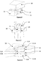
- the figure 1 illustrates a portion of a printed circuit 10 of an electronic payment terminal conventionally having an upper half-shell, or upper cover, and a lower half-shell, or lower cover (not shown).
- the printed circuit 10 comprises a housing 11 opening, formed to be through in the thickness of the printed circuit 10, for example at the keyboard, the display, the card reader, that is to say any area of the electronic payment terminal where information is to be protected, or in the open spaces of the terminal that could accommodate spyware, or to detect attempts to dismantle the payment terminal electronic installation location (fixed mounting case on a dispenser or countertop).
- two safety circuits 12, 13 each formed of a safety track are provided inside the printed circuit 10.
- the safety tracks are provided at the inner layers of the printed circuit 10, in its thickness, and do not flop on the surface of the printed circuit 10 as is the case in the prior art.
- the two security circuits 12, 13 are coplanar, that is to say that they each extend in a plane corresponding to an inner layer of the printed circuit, the different inner layers being parallel to each other.
- the safety tracks are made for example by copper layers etched in the printed circuit 10, for example by photochemical process as for the other tracks of the printed circuit, and are interrupted at the housing 11.
- a metallization phase (typically used for producing metallized holes) can be used to improve the quality of the contact surface inside the housing 11.
- each track follows the circumference of the housing 11, while flush with its vertical wall so as to be accessible, and is interrupted in an "insulating" area 121, 131, thus forming several portions of tracks not connected to each other.
- the printed circuit 10 comprises on its lower and upper surfaces respectively another type of circuit consisting of partially metallized conductive tracks, called the guard ring 14.
- These guard rings 14 provide additional security and make it possible to detect if contact is established on the surface of the printed circuit 10, for example in the case where a conductive liquid would be injected, thereby causing closure of the circuit for neutralizing the safety device, according to the techniques of the prior art.
- the cylindrical form of housing illustrated on this figure 1 allows an optimal efficiency of operation of the safety device, because the deformable safety element inserted therein, also of cylindrical shape, can deform uniformly and thus ensure effective closure of the safety circuit or circuits.
- Any other form, for example oblong, housing and deformable element, to address the problem is of course possible, also depending on the implementation constraints of the components on the circuit the position of the printed circuit board inside the electronic payment terminal, etc.
- the housing can be obtained by drilling or milling, which allows obtaining rounded corners and thus allows the deformable element to have a shape closer to the profile of the housing in which it is inserted .
- FIGS. 2 and 3 illustrate a first embodiment of a safety device 20 corresponding to a deformable safety element 20 inserted into the housing 11 described above in connection with the figure 1 .
- this deformable safety element 20 therefore has a substantially cylindrical shape and comprises a first central insulating portion 21 (for example made of unloaded silicone), corresponding to a support (having, for example, an "H" profile when looking at the printed circuit vertically) making it possible to maintain a second conductive portion 22 (for example of carbon-loaded silicone), covering the first part 21 over part of its height and a part of its circumference.
- a first central insulating portion 21 for example made of unloaded silicone
- a support having, for example, an "H" profile when looking at the printed circuit vertically
- a second conductive portion 22 for example of carbon-loaded silicone
- the two parts 21, 22, for example overmoulded or assembled, are made of elastomer (for example silicone) and are therefore deformable.
- the elastomer portion 22 is deformed by "swelling" in the manner of a barrel: its height decreases while its circumference increases, the portion 21 is also deformed by training.
- the first portion 21 is insulating, for example uncharged silicone, while the second portion 22 is conductive.
- This second portion 22 is for example made by molding a filled material (for example silicone loaded with carbon) and then placed in the mold in which the molding of the unfilled material is performed for the part 21, to perform a overmolding.
- the charged portion 22 is cut in conductive material before being overmolded.
- the part 22 thus has a conductive surface which, when the deformable element 20 is inserted into the housing and deformed (or compressed), to close the safety circuits 12 and 13 at the positions 121 and 131 illustrated in FIG. figure 1 .
- the figure 2 represents the security device 20 in its "rest" position, that is to say before its deformation, here by assembling the two shells of the electronic payment terminal (not shown).
- the peripheral conductive surface of the portion 22 is set back from the walls of the housing 11 and the safety circuits 12, 13 are then open. Furthermore, the ends of the support 21 (here corresponding to both sides of the "H") are slightly raised relative to the lower and upper surfaces of the printed circuit 10.
- the figure 3 for its part, it represents the security device 20 when it is deformed, for example when the electronic payment terminal is assembled and in the normal "use" configuration.
- the upper and lower surfaces of the support 21 are compressed under two support elements (not shown) on either side of the housing 11, in the same plane as the lower and upper surfaces of the printed circuit 10.
- the compression forces are transmitted to the part 22, causing its deformation and the contacting of its peripheral surface with the track portions of the safety circuits 12, 13 flush inside the housing 11.
- the safety circuits 12, 13 are then closed.
- the support elements for compressing the safety device are for example constituted by the upper and lower half-shells of the electronic payment terminal, or by one or more components mounted on the printed circuit board 10, as described below in relation to with a variant of this first embodiment illustrated in figure 4 .
- the figure 4 illustrates, according to a variant of this first embodiment, an example of a support element 30 mounted on the printed circuit, above the housing in which is inserted a safety device as illustrated in FIG. Figures 2 and 3 . It is therefore the component 30 which exerts pressure on the deformable element 20 and more precisely causes the deformation of the part 22, thus closing the safety circuits 12 and 13 as already described above.
- the housing 11 may be non-opening, or blind, for example formed in a device of the type "Cache I / O" which consists of a complementary safety device soldered on the surface of the printed circuit, intended to protect one or more sensitive components, such as the connections of a card reader or a security device.
- a device of the type "Cache I / O" which consists of a complementary safety device soldered on the surface of the printed circuit, intended to protect one or more sensitive components, such as the connections of a card reader or a security device.
- the support 21 of the safety device 20 is provided with a passage through which can be inserted a fixing means, for example a screw 40, for assembling two parts, or two components, of the electronic payment terminal on the one hand and other of the printed circuit 10. It is the insertion of this fixing means in the deformable safety element which causes its deformation inside the housing and thus the closure of the security circuit or circuits concerned, such as previously described.
- a fixing means for example a screw 40
- the figure 6 illustrates a third embodiment of the safety device embedded in the housing 11, wherein the safety device 50 comprises two deformable security elements 52A, 52B, each having a substantially cylindrical shape.
- deformable safety elements 52A, 52B are arranged one on the other along a longitudinal axis of the housing 11, that is to say along an axis passing through the printed circuit 10 from bottom to top.
- Each deformable security element 52A, 52B has a height substantially equal to half the height of the deformable safety element 20 described in the first and second embodiments, but it could be otherwise (two deformable elements of different size ).
- These security deformable elements 52A, 52B also include a conductive peripheral surface similar to that of the first and second embodiments.
- Two "support" end 51A, 51B, having a generally cylindrical shape provided with a flange 511A, 511B are symmetrically arranged on either side of the elements 52A, 52B, along said longitudinal axis of the housing 11.
- These flanges 511A , 511B have a diameter greater than the diameter of the housing 11, and allow, once positioned, to cover the latter so as to improve the sealing of the device and its security against attacks.
- the deformable safety elements 52A, 52B and the "support" end elements 51A, 51B are deformable, and more specifically compressible.
- the elements 52A, 52B deform under the effect of a compression force "swelling": their height decreases while their circumference increases.
- each of these elements 52A, 52B comes into contact with the track portions of the safety circuits 12, 13 flush with the inner periphery of the housing 11, which closes the safety circuits 12, 13.
- the elements 52A, 52B are in contact with one another via a conductive surface when the security element is compressed.
- the flanges 511A, 511B make it possible to keep the conductive front surfaces of the two elements 52A, 52B disjointed as long as the security element is not under pressure.
- the two safety circuits 12, 13 are closed jointly by the two elements 52A, 52B since the current flows between the conductive peripheral surfaces of each element 52A, 52B.
- the elements 52A, 52B are in contact with one another via an insulating surface.
- the safety circuits 12, 13 are independent since the current does not flow between the conductive peripheral surfaces of each element 52A, 52B.
- the independence of the two circuits 12, 13 makes it more difficult to neutralize one or the other.
- the two superimposed circuits 12, 13 thus protect each other. It is possible to jointly monitor the opening of the circuits 12, 13, their grounding and their short-circuit, which makes the attacks more complicated to implement.
- the security device 20, 50 may be covered with a flexible mesh, for example a flexible printed circuit covered with a plurality of interleaved conductive tracks, adhesively affixed to the safety device before the half the electronic payment terminal are assembled.
- a flexible mesh is able to deform without losing efficiency and can therefore be positioned on the printed circuit when the deformable safety element or elements are in the "rest” position and then marry the surface of the circuit board once the deformable security element or elements in "compressed” position in the housing. This trellis therefore aims to strengthen the protection of access to the safety device.
- the flexible mesh alone, is not sufficient to achieve the forces required to compress the safety device 20, 50.
- it can be in place a support on one of the terminals of the terminal of electronic payment.
- the bonding will be done on the flexible mesh and will not allow a sufficient maintenance of the support to compress the safety device 20, 50 and ensure the closure of the circuits. security 12, 13.
- This new approach to securing an electronic payment terminal has several advantages over the techniques of the prior art.
- One of the advantages lies in the positioning of the security circuits 12, 13 at the inner layers of the printed circuit 10, which makes the latter less accessible and therefore more difficult to neutralize.
- Another advantage lies in the particular configuration of a housing opening on the two surfaces of the printed circuit, for detecting an attempt to intrude from one or other of the faces of the printed circuit. For example, if an attacker attempts to open the payment terminal, for example by removing the upper half-shell or the lower half-shell, the security device ceases to be compressed and returns to its original shape, thereby opening the door. one or the other of the safety circuits 12, 13. Thus, the safety device ceases to be compressed regardless of the half-shell removed, unlike the prior art which makes it possible to detect only the withdrawal of the half-shell. shell on the side where is installed a "false key" for example.
- the (or) element (s) deformable (s) 20, 52A, 52B behaves (s) as an insulating plug when (s) is or are compressed (s) and "inflated (s)" within the housing 11, thereby preventing the liquid to enter the housing 11 and come into contact with the tracks of the safety circuits 12, 13. Therefore, if the attacker then dismounts the terminal, the security circuits 12, 13 open when the deformable element returns to its original shape following the release of the pressure applied to it, and the intrusion attempt can be detected.
- the solution of the invention requires less effort, or in all cases below the minimum forces required in the prior art, for the security element to deform and comes into contact with the conductive tracks 12, 13. This is due in particular to the fact that the elastomer in which is made l The security element deforms more easily, because of its flexibility, than the materials of the "false keys" of the prior art.
- the compression of the element 22 of elastomer requires the full effort only when closing the electronic payment terminal, during the assembly of the two shells of the terminal.
- a compression force of less than 200 gF is sufficient to deform the deformable element in a deformation of about 0.9 mm, whereas a force of about 300 gF was for example necessary in the prior art, to activate the metal dome requiring a deformation between 0.9 and 1.4 mm depending on the hardness of the elastomer.
- the force generated by the mounting of the component remains limited to the deformation of the elastomer and not to its compression, but allows to deform sufficiently to close the safety circuits 12, 13.
- the force required to maintain the electrical contact by deformation of the deformable safety element is therefore less important than in the solutions of the prior art.
- the solution is thus more reliable in the long term because the deformable safety element is subjected to lower forces, not necessarily causing its total compression, and its deformation capacity is less likely to vary over time.
Landscapes
- Engineering & Computer Science (AREA)
- Computer Hardware Design (AREA)
- Theoretical Computer Science (AREA)
- General Physics & Mathematics (AREA)
- Physics & Mathematics (AREA)
- Software Systems (AREA)
- General Engineering & Computer Science (AREA)
- Computer Security & Cryptography (AREA)
- Microelectronics & Electronic Packaging (AREA)
- Storage Device Security (AREA)
- Burglar Alarm Systems (AREA)
- Casings For Electric Apparatus (AREA)
- Pinball Game Machines (AREA)
- Structure Of Printed Boards (AREA)
- Condensed Matter Physics & Semiconductors (AREA)
Applications Claiming Priority (1)
| Application Number | Priority Date | Filing Date | Title |
|---|---|---|---|
| FR1853073A FR3079947B1 (fr) | 2018-04-09 | 2018-04-09 | Dispositif de securite d'un terminal de paiement comprenant un element de securite encastre. |
Publications (2)
| Publication Number | Publication Date |
|---|---|
| EP3553691A1 true EP3553691A1 (de) | 2019-10-16 |
| EP3553691B1 EP3553691B1 (de) | 2021-03-10 |
Family
ID=62455734
Family Applications (1)
| Application Number | Title | Priority Date | Filing Date |
|---|---|---|---|
| EP19167886.1A Active EP3553691B1 (de) | 2018-04-09 | 2019-04-08 | Sicherheitsvorrichtung für ein zahlungsendgerät, die ein eingebautes sicherheitselement umfasst |
Country Status (5)
| Country | Link |
|---|---|
| US (1) | US11386242B2 (de) |
| EP (1) | EP3553691B1 (de) |
| CA (1) | CA3039712A1 (de) |
| ES (1) | ES2867955T3 (de) |
| FR (1) | FR3079947B1 (de) |
Families Citing this family (3)
| Publication number | Priority date | Publication date | Assignee | Title |
|---|---|---|---|---|
| FR3105468B1 (fr) * | 2019-12-20 | 2022-02-11 | Ingenico Group | Dispositif d’interconnexion de deux terminaux |
| FR3115897B1 (fr) * | 2020-11-04 | 2023-06-09 | Banks And Acquirers Int Holding | Module de sécurité, terminal de paiement électronique, procédé de détection correspondant. |
| CN120239868A (zh) * | 2022-11-18 | 2025-07-01 | 捷普有限公司 | 用于支付终端的安全操作管理模块的装置、系统和方法 |
Citations (2)
| Publication number | Priority date | Publication date | Assignee | Title |
|---|---|---|---|---|
| FR2929042A1 (fr) * | 2008-03-21 | 2009-09-25 | Sagem Monetel Soc Par Actions | Dispositif de protection d'un systeme electronique |
| EP2146562A1 (de) * | 2008-07-16 | 2010-01-20 | Compagnie Industrielle et Financiere d'Ingenierie "Ingenico" | Schutzvorrichtung einer elektronischen Komponente |
Family Cites Families (2)
| Publication number | Priority date | Publication date | Assignee | Title |
|---|---|---|---|---|
| US20050059859A1 (en) * | 2003-09-15 | 2005-03-17 | Gregory Konstorum | Method and system for mounting and securing parts inside an instrument housing |
| US8736513B2 (en) * | 2010-01-27 | 2014-05-27 | Sarantel Limited | Dielectrically loaded antenna and radio communication apparatus |
-
2018
- 2018-04-09 FR FR1853073A patent/FR3079947B1/fr active Active
-
2019
- 2019-04-08 CA CA3039712A patent/CA3039712A1/en active Pending
- 2019-04-08 ES ES19167886T patent/ES2867955T3/es active Active
- 2019-04-08 EP EP19167886.1A patent/EP3553691B1/de active Active
- 2019-04-08 US US16/377,905 patent/US11386242B2/en active Active
Patent Citations (2)
| Publication number | Priority date | Publication date | Assignee | Title |
|---|---|---|---|---|
| FR2929042A1 (fr) * | 2008-03-21 | 2009-09-25 | Sagem Monetel Soc Par Actions | Dispositif de protection d'un systeme electronique |
| EP2146562A1 (de) * | 2008-07-16 | 2010-01-20 | Compagnie Industrielle et Financiere d'Ingenierie "Ingenico" | Schutzvorrichtung einer elektronischen Komponente |
Also Published As
| Publication number | Publication date |
|---|---|
| ES2867955T3 (es) | 2021-10-21 |
| US11386242B2 (en) | 2022-07-12 |
| FR3079947B1 (fr) | 2020-04-17 |
| EP3553691B1 (de) | 2021-03-10 |
| FR3079947A1 (fr) | 2019-10-11 |
| CA3039712A1 (en) | 2019-10-09 |
| US20190311159A1 (en) | 2019-10-10 |
Similar Documents
| Publication | Publication Date | Title |
|---|---|---|
| EP3553691B1 (de) | Sicherheitsvorrichtung für ein zahlungsendgerät, die ein eingebautes sicherheitselement umfasst | |
| WO2003012230A1 (fr) | Poignee d'ouvrant pour vehicule automobile | |
| EP2241997B1 (de) | Speicherkartenleser | |
| CA2654060A1 (fr) | Dispositif de protection contre les intrusions d'appareils electroniques | |
| EP3371735B1 (de) | Körper eines speicherkartenlesers mit einem schutznetz auf beiden seiten | |
| CA2983704C (fr) | Detection d'ouverture d'un dispositif de saisie de donnees | |
| EP2062237B1 (de) | Detektor eines versuchs, einen riegel zu brechen, riegel, tür und alarmsystem mit einem solchen detektor | |
| EP3295365B1 (de) | Erkennung der öffnung einer dateneingabevorrichtung | |
| WO2008077964A1 (fr) | Boitier securise | |
| EP4133440B1 (de) | Elektronische bezahlvorrichtung mit mitteln zur zugriffsblockierung auf ein datenspeichermodul | |
| CA3196577A1 (fr) | Module de securite, terminal de paiement e?lectronique, procede de d etection correspondant | |
| WO2022194889A1 (fr) | Dispositif de paiement intégré dans une borne de paiement électronique non surveillée | |
| FR2985154A1 (fr) | Circuit imprime flexible. | |
| FR3080202A1 (fr) | Dispositif de securisation d'un volume dans un terminal de paiement electronique. | |
| WO2024133863A1 (fr) | Terminal de paiement électronique à drainage de liquide indésirable optimisé | |
| EP1365305B1 (de) | Eindringgeschütztes Gehäuse mit Widerstandsmaschennetzwerk | |
| FR3164304A1 (fr) | terminal électronique et système de sécurité | |
| FR3153809A1 (fr) | Bouchon de sécurité | |
| FR3038780A1 (fr) | Connecteur de circuit integre securise | |
| FR2910584A1 (fr) | Dispositif de decharge de pression | |
| FR2885761A1 (fr) | Presentoir securise, notamment pour appareil muni d'une prise electrique | |
| FR2852888A1 (fr) | Rouleau de circulation | |
| FR3051941A1 (fr) | Corps de lecteur de carte a memoire securise | |
| WO2016142487A1 (fr) | Touche sécurisée de clavier analogique, procédé et module de détection d'intrusion, terminal de paiement électronique, programme et support d'enregistrement correspondants | |
| FR2985338A1 (fr) | Clavier securise |
Legal Events
| Date | Code | Title | Description |
|---|---|---|---|
| PUAI | Public reference made under article 153(3) epc to a published international application that has entered the european phase |
Free format text: ORIGINAL CODE: 0009012 |
|
| STAA | Information on the status of an ep patent application or granted ep patent |
Free format text: STATUS: THE APPLICATION HAS BEEN PUBLISHED |
|
| AK | Designated contracting states |
Kind code of ref document: A1 Designated state(s): AL AT BE BG CH CY CZ DE DK EE ES FI FR GB GR HR HU IE IS IT LI LT LU LV MC MK MT NL NO PL PT RO RS SE SI SK SM TR |
|
| AX | Request for extension of the european patent |
Extension state: BA ME |
|
| STAA | Information on the status of an ep patent application or granted ep patent |
Free format text: STATUS: REQUEST FOR EXAMINATION WAS MADE |
|
| 17P | Request for examination filed |
Effective date: 20200410 |
|
| RBV | Designated contracting states (corrected) |
Designated state(s): AL AT BE BG CH CY CZ DE DK EE ES FI FR GB GR HR HU IE IS IT LI LT LU LV MC MK MT NL NO PL PT RO RS SE SI SK SM TR |
|
| GRAP | Despatch of communication of intention to grant a patent |
Free format text: ORIGINAL CODE: EPIDOSNIGR1 |
|
| STAA | Information on the status of an ep patent application or granted ep patent |
Free format text: STATUS: GRANT OF PATENT IS INTENDED |
|
| INTG | Intention to grant announced |
Effective date: 20201113 |
|
| GRAS | Grant fee paid |
Free format text: ORIGINAL CODE: EPIDOSNIGR3 |
|
| GRAA | (expected) grant |
Free format text: ORIGINAL CODE: 0009210 |
|
| STAA | Information on the status of an ep patent application or granted ep patent |
Free format text: STATUS: THE PATENT HAS BEEN GRANTED |
|
| AK | Designated contracting states |
Kind code of ref document: B1 Designated state(s): AL AT BE BG CH CY CZ DE DK EE ES FI FR GB GR HR HU IE IS IT LI LT LU LV MC MK MT NL NO PL PT RO RS SE SI SK SM TR |
|
| REG | Reference to a national code |
Ref country code: GB Ref legal event code: FG4D Free format text: NOT ENGLISH |
|
| REG | Reference to a national code |
Ref country code: CH Ref legal event code: EP Ref country code: AT Ref legal event code: REF Ref document number: 1370641 Country of ref document: AT Kind code of ref document: T Effective date: 20210315 |
|
| REG | Reference to a national code |
Ref country code: IE Ref legal event code: FG4D Free format text: LANGUAGE OF EP DOCUMENT: FRENCH |
|
| REG | Reference to a national code |
Ref country code: DE Ref legal event code: R096 Ref document number: 602019003028 Country of ref document: DE |
|
| REG | Reference to a national code |
Ref country code: LT Ref legal event code: MG9D |
|
| PG25 | Lapsed in a contracting state [announced via postgrant information from national office to epo] |
Ref country code: NO Free format text: LAPSE BECAUSE OF FAILURE TO SUBMIT A TRANSLATION OF THE DESCRIPTION OR TO PAY THE FEE WITHIN THE PRESCRIBED TIME-LIMIT Effective date: 20210610 Ref country code: LT Free format text: LAPSE BECAUSE OF FAILURE TO SUBMIT A TRANSLATION OF THE DESCRIPTION OR TO PAY THE FEE WITHIN THE PRESCRIBED TIME-LIMIT Effective date: 20210310 Ref country code: GR Free format text: LAPSE BECAUSE OF FAILURE TO SUBMIT A TRANSLATION OF THE DESCRIPTION OR TO PAY THE FEE WITHIN THE PRESCRIBED TIME-LIMIT Effective date: 20210611 Ref country code: FI Free format text: LAPSE BECAUSE OF FAILURE TO SUBMIT A TRANSLATION OF THE DESCRIPTION OR TO PAY THE FEE WITHIN THE PRESCRIBED TIME-LIMIT Effective date: 20210310 Ref country code: HR Free format text: LAPSE BECAUSE OF FAILURE TO SUBMIT A TRANSLATION OF THE DESCRIPTION OR TO PAY THE FEE WITHIN THE PRESCRIBED TIME-LIMIT Effective date: 20210310 Ref country code: BG Free format text: LAPSE BECAUSE OF FAILURE TO SUBMIT A TRANSLATION OF THE DESCRIPTION OR TO PAY THE FEE WITHIN THE PRESCRIBED TIME-LIMIT Effective date: 20210610 |
|
| REG | Reference to a national code |
Ref country code: AT Ref legal event code: MK05 Ref document number: 1370641 Country of ref document: AT Kind code of ref document: T Effective date: 20210310 |
|
| REG | Reference to a national code |
Ref country code: NL Ref legal event code: MP Effective date: 20210310 |
|
| PG25 | Lapsed in a contracting state [announced via postgrant information from national office to epo] |
Ref country code: RS Free format text: LAPSE BECAUSE OF FAILURE TO SUBMIT A TRANSLATION OF THE DESCRIPTION OR TO PAY THE FEE WITHIN THE PRESCRIBED TIME-LIMIT Effective date: 20210310 Ref country code: LV Free format text: LAPSE BECAUSE OF FAILURE TO SUBMIT A TRANSLATION OF THE DESCRIPTION OR TO PAY THE FEE WITHIN THE PRESCRIBED TIME-LIMIT Effective date: 20210310 Ref country code: SE Free format text: LAPSE BECAUSE OF FAILURE TO SUBMIT A TRANSLATION OF THE DESCRIPTION OR TO PAY THE FEE WITHIN THE PRESCRIBED TIME-LIMIT Effective date: 20210310 |
|
| PG25 | Lapsed in a contracting state [announced via postgrant information from national office to epo] |
Ref country code: NL Free format text: LAPSE BECAUSE OF FAILURE TO SUBMIT A TRANSLATION OF THE DESCRIPTION OR TO PAY THE FEE WITHIN THE PRESCRIBED TIME-LIMIT Effective date: 20210310 |
|
| REG | Reference to a national code |
Ref country code: ES Ref legal event code: FG2A Ref document number: 2867955 Country of ref document: ES Kind code of ref document: T3 Effective date: 20211021 |
|
| PG25 | Lapsed in a contracting state [announced via postgrant information from national office to epo] |
Ref country code: CZ Free format text: LAPSE BECAUSE OF FAILURE TO SUBMIT A TRANSLATION OF THE DESCRIPTION OR TO PAY THE FEE WITHIN THE PRESCRIBED TIME-LIMIT Effective date: 20210310 Ref country code: EE Free format text: LAPSE BECAUSE OF FAILURE TO SUBMIT A TRANSLATION OF THE DESCRIPTION OR TO PAY THE FEE WITHIN THE PRESCRIBED TIME-LIMIT Effective date: 20210310 Ref country code: SM Free format text: LAPSE BECAUSE OF FAILURE TO SUBMIT A TRANSLATION OF THE DESCRIPTION OR TO PAY THE FEE WITHIN THE PRESCRIBED TIME-LIMIT Effective date: 20210310 Ref country code: AT Free format text: LAPSE BECAUSE OF FAILURE TO SUBMIT A TRANSLATION OF THE DESCRIPTION OR TO PAY THE FEE WITHIN THE PRESCRIBED TIME-LIMIT Effective date: 20210310 |
|
| PG25 | Lapsed in a contracting state [announced via postgrant information from national office to epo] |
Ref country code: SK Free format text: LAPSE BECAUSE OF FAILURE TO SUBMIT A TRANSLATION OF THE DESCRIPTION OR TO PAY THE FEE WITHIN THE PRESCRIBED TIME-LIMIT Effective date: 20210310 Ref country code: PT Free format text: LAPSE BECAUSE OF FAILURE TO SUBMIT A TRANSLATION OF THE DESCRIPTION OR TO PAY THE FEE WITHIN THE PRESCRIBED TIME-LIMIT Effective date: 20210712 Ref country code: RO Free format text: LAPSE BECAUSE OF FAILURE TO SUBMIT A TRANSLATION OF THE DESCRIPTION OR TO PAY THE FEE WITHIN THE PRESCRIBED TIME-LIMIT Effective date: 20210310 Ref country code: PL Free format text: LAPSE BECAUSE OF FAILURE TO SUBMIT A TRANSLATION OF THE DESCRIPTION OR TO PAY THE FEE WITHIN THE PRESCRIBED TIME-LIMIT Effective date: 20210310 Ref country code: IS Free format text: LAPSE BECAUSE OF FAILURE TO SUBMIT A TRANSLATION OF THE DESCRIPTION OR TO PAY THE FEE WITHIN THE PRESCRIBED TIME-LIMIT Effective date: 20210710 |
|
| REG | Reference to a national code |
Ref country code: DE Ref legal event code: R097 Ref document number: 602019003028 Country of ref document: DE |
|
| PG25 | Lapsed in a contracting state [announced via postgrant information from national office to epo] |
Ref country code: LU Free format text: LAPSE BECAUSE OF NON-PAYMENT OF DUE FEES Effective date: 20210408 |
|
| PLBE | No opposition filed within time limit |
Free format text: ORIGINAL CODE: 0009261 |
|
| STAA | Information on the status of an ep patent application or granted ep patent |
Free format text: STATUS: NO OPPOSITION FILED WITHIN TIME LIMIT |
|
| REG | Reference to a national code |
Ref country code: BE Ref legal event code: MM Effective date: 20210430 |
|
| PG25 | Lapsed in a contracting state [announced via postgrant information from national office to epo] |
Ref country code: MC Free format text: LAPSE BECAUSE OF FAILURE TO SUBMIT A TRANSLATION OF THE DESCRIPTION OR TO PAY THE FEE WITHIN THE PRESCRIBED TIME-LIMIT Effective date: 20210310 Ref country code: DK Free format text: LAPSE BECAUSE OF FAILURE TO SUBMIT A TRANSLATION OF THE DESCRIPTION OR TO PAY THE FEE WITHIN THE PRESCRIBED TIME-LIMIT Effective date: 20210310 Ref country code: AL Free format text: LAPSE BECAUSE OF FAILURE TO SUBMIT A TRANSLATION OF THE DESCRIPTION OR TO PAY THE FEE WITHIN THE PRESCRIBED TIME-LIMIT Effective date: 20210310 |
|
| 26N | No opposition filed |
Effective date: 20211213 |
|
| REG | Reference to a national code |
Ref country code: GB Ref legal event code: 732E Free format text: REGISTERED BETWEEN 20220127 AND 20220202 |
|
| PG25 | Lapsed in a contracting state [announced via postgrant information from national office to epo] |
Ref country code: SI Free format text: LAPSE BECAUSE OF FAILURE TO SUBMIT A TRANSLATION OF THE DESCRIPTION OR TO PAY THE FEE WITHIN THE PRESCRIBED TIME-LIMIT Effective date: 20210310 |
|
| PG25 | Lapsed in a contracting state [announced via postgrant information from national office to epo] |
Ref country code: IT Free format text: LAPSE BECAUSE OF FAILURE TO SUBMIT A TRANSLATION OF THE DESCRIPTION OR TO PAY THE FEE WITHIN THE PRESCRIBED TIME-LIMIT Effective date: 20210310 Ref country code: IE Free format text: LAPSE BECAUSE OF NON-PAYMENT OF DUE FEES Effective date: 20210408 |
|
| PG25 | Lapsed in a contracting state [announced via postgrant information from national office to epo] |
Ref country code: IS Free format text: LAPSE BECAUSE OF FAILURE TO SUBMIT A TRANSLATION OF THE DESCRIPTION OR TO PAY THE FEE WITHIN THE PRESCRIBED TIME-LIMIT Effective date: 20210710 |
|
| REG | Reference to a national code |
Ref country code: DE Ref legal event code: R081 Ref document number: 602019003028 Country of ref document: DE Owner name: BANKS AND ACQUIRES INTERNATIONAL HOLDING, FR Free format text: FORMER OWNER: INGENICO GROUP, PARIS, FR Ref country code: DE Ref legal event code: R082 Ref document number: 602019003028 Country of ref document: DE Representative=s name: STUMPF PATENTANWAELTE PARTGMBB, DE Ref country code: DE Ref legal event code: R081 Ref document number: 602019003028 Country of ref document: DE Owner name: BANKS AND ACQUIRERS INTERNATIONAL HOLDING, FR Free format text: FORMER OWNER: INGENICO GROUP, PARIS, FR |
|
| PG25 | Lapsed in a contracting state [announced via postgrant information from national office to epo] |
Ref country code: BE Free format text: LAPSE BECAUSE OF NON-PAYMENT OF DUE FEES Effective date: 20210430 |
|
| REG | Reference to a national code |
Ref country code: CH Ref legal event code: PL |
|
| PG25 | Lapsed in a contracting state [announced via postgrant information from national office to epo] |
Ref country code: LI Free format text: LAPSE BECAUSE OF NON-PAYMENT OF DUE FEES Effective date: 20220430 Ref country code: CH Free format text: LAPSE BECAUSE OF NON-PAYMENT OF DUE FEES Effective date: 20220430 |
|
| PG25 | Lapsed in a contracting state [announced via postgrant information from national office to epo] |
Ref country code: CY Free format text: LAPSE BECAUSE OF FAILURE TO SUBMIT A TRANSLATION OF THE DESCRIPTION OR TO PAY THE FEE WITHIN THE PRESCRIBED TIME-LIMIT Effective date: 20210310 |
|
| PG25 | Lapsed in a contracting state [announced via postgrant information from national office to epo] |
Ref country code: HU Free format text: LAPSE BECAUSE OF FAILURE TO SUBMIT A TRANSLATION OF THE DESCRIPTION OR TO PAY THE FEE WITHIN THE PRESCRIBED TIME-LIMIT; INVALID AB INITIO Effective date: 20190408 |
|
| PG25 | Lapsed in a contracting state [announced via postgrant information from national office to epo] |
Ref country code: MK Free format text: LAPSE BECAUSE OF FAILURE TO SUBMIT A TRANSLATION OF THE DESCRIPTION OR TO PAY THE FEE WITHIN THE PRESCRIBED TIME-LIMIT Effective date: 20210310 |
|
| PG25 | Lapsed in a contracting state [announced via postgrant information from national office to epo] |
Ref country code: TR Free format text: LAPSE BECAUSE OF FAILURE TO SUBMIT A TRANSLATION OF THE DESCRIPTION OR TO PAY THE FEE WITHIN THE PRESCRIBED TIME-LIMIT Effective date: 20210310 |
|
| PG25 | Lapsed in a contracting state [announced via postgrant information from national office to epo] |
Ref country code: MT Free format text: LAPSE BECAUSE OF FAILURE TO SUBMIT A TRANSLATION OF THE DESCRIPTION OR TO PAY THE FEE WITHIN THE PRESCRIBED TIME-LIMIT Effective date: 20210310 |
|
| REG | Reference to a national code |
Ref country code: DE Ref legal event code: R081 Ref document number: 602019003028 Country of ref document: DE Owner name: BANKS AND ACQUIRERS INTERNATIONAL HOLDING, FR Free format text: FORMER OWNER: BANKS AND ACQUIRES INTERNATIONAL HOLDING, SURESNES, FR |
|
| PGFP | Annual fee paid to national office [announced via postgrant information from national office to epo] |
Ref country code: DE Payment date: 20250422 Year of fee payment: 7 |
|
| PGFP | Annual fee paid to national office [announced via postgrant information from national office to epo] |
Ref country code: GB Payment date: 20250423 Year of fee payment: 7 Ref country code: ES Payment date: 20250530 Year of fee payment: 7 |
|
| PGFP | Annual fee paid to national office [announced via postgrant information from national office to epo] |
Ref country code: FR Payment date: 20250429 Year of fee payment: 7 |
|
| REG | Reference to a national code |
Ref country code: ES Ref legal event code: PC2A Owner name: BANKS AND ACQUIRERS INTERNATIONAL HOLDING Effective date: 20250930 |
|
| P01 | Opt-out of the competence of the unified patent court (upc) registered |
Free format text: CASE NUMBER: UPC_APP_0000329_3553691/2026 Effective date: 20260106 |