EP3553588B1 - System for use in imageing in air - Google Patents
System for use in imageing in air Download PDFInfo
- Publication number
- EP3553588B1 EP3553588B1 EP17878470.8A EP17878470A EP3553588B1 EP 3553588 B1 EP3553588 B1 EP 3553588B1 EP 17878470 A EP17878470 A EP 17878470A EP 3553588 B1 EP3553588 B1 EP 3553588B1
- Authority
- EP
- European Patent Office
- Prior art keywords
- retroreflective
- transflective mirror
- sub
- polarized light
- light
- Prior art date
- Legal status (The legal status is an assumption and is not a legal conclusion. Google has not performed a legal analysis and makes no representation as to the accuracy of the status listed.)
- Active
Links
Images




Classifications
-
- G—PHYSICS
- G02—OPTICS
- G02B—OPTICAL ELEMENTS, SYSTEMS OR APPARATUS
- G02B5/00—Optical elements other than lenses
- G02B5/12—Reflex reflectors
-
- G—PHYSICS
- G02—OPTICS
- G02B—OPTICAL ELEMENTS, SYSTEMS OR APPARATUS
- G02B5/00—Optical elements other than lenses
- G02B5/12—Reflex reflectors
- G02B5/122—Reflex reflectors cube corner, trihedral or triple reflector type
- G02B5/124—Reflex reflectors cube corner, trihedral or triple reflector type plural reflecting elements forming part of a unitary plate or sheet
-
- G—PHYSICS
- G02—OPTICS
- G02B—OPTICAL ELEMENTS, SYSTEMS OR APPARATUS
- G02B1/00—Optical elements characterised by the material of which they are made; Optical coatings for optical elements
- G02B1/10—Optical coatings produced by application to, or surface treatment of, optical elements
- G02B1/11—Anti-reflection coatings
-
- G—PHYSICS
- G02—OPTICS
- G02B—OPTICAL ELEMENTS, SYSTEMS OR APPARATUS
- G02B27/00—Optical systems or apparatus not provided for by any of the groups G02B1/00 - G02B26/00, G02B30/00
- G02B27/10—Beam splitting or combining systems
- G02B27/14—Beam splitting or combining systems operating by reflection only
-
- G—PHYSICS
- G02—OPTICS
- G02B—OPTICAL ELEMENTS, SYSTEMS OR APPARATUS
- G02B30/00—Optical systems or apparatus for producing three-dimensional [3D] effects, e.g. stereoscopic images
- G02B30/20—Optical systems or apparatus for producing three-dimensional [3D] effects, e.g. stereoscopic images by providing first and second parallax images to an observer's left and right eyes
- G02B30/34—Stereoscopes providing a stereoscopic pair of separated images corresponding to parallactically displaced views of the same object, e.g. three-dimensional [3D] slide viewers
- G02B30/35—Stereoscopes providing a stereoscopic pair of separated images corresponding to parallactically displaced views of the same object, e.g. three-dimensional [3D] slide viewers using reflective optical elements in the optical path between the images and the observer
-
- G—PHYSICS
- G02—OPTICS
- G02B—OPTICAL ELEMENTS, SYSTEMS OR APPARATUS
- G02B30/00—Optical systems or apparatus for producing three-dimensional [3D] effects, e.g. stereoscopic images
- G02B30/50—Optical systems or apparatus for producing three-dimensional [3D] effects, e.g. stereoscopic images the image being built up from image elements distributed over a three-dimensional [3D] volume, e.g. voxels
- G02B30/56—Optical systems or apparatus for producing three-dimensional [3D] effects, e.g. stereoscopic images the image being built up from image elements distributed over a three-dimensional [3D] volume, e.g. voxels by projecting aerial or floating images
-
- G—PHYSICS
- G02—OPTICS
- G02B—OPTICAL ELEMENTS, SYSTEMS OR APPARATUS
- G02B5/00—Optical elements other than lenses
- G02B5/12—Reflex reflectors
- G02B5/122—Reflex reflectors cube corner, trihedral or triple reflector type
-
- G—PHYSICS
- G02—OPTICS
- G02B—OPTICAL ELEMENTS, SYSTEMS OR APPARATUS
- G02B5/00—Optical elements other than lenses
- G02B5/12—Reflex reflectors
- G02B5/126—Reflex reflectors including curved refracting surface
- G02B5/128—Reflex reflectors including curved refracting surface transparent spheres being embedded in matrix
-
- G—PHYSICS
- G02—OPTICS
- G02B—OPTICAL ELEMENTS, SYSTEMS OR APPARATUS
- G02B5/00—Optical elements other than lenses
- G02B5/12—Reflex reflectors
- G02B5/126—Reflex reflectors including curved refracting surface
- G02B5/13—Reflex reflectors including curved refracting surface plural curved refracting elements forming part of a unitary body
-
- G—PHYSICS
- G02—OPTICS
- G02B—OPTICAL ELEMENTS, SYSTEMS OR APPARATUS
- G02B5/00—Optical elements other than lenses
- G02B5/30—Polarising elements
- G02B5/3083—Birefringent or phase retarding elements
-
- G—PHYSICS
- G03—PHOTOGRAPHY; CINEMATOGRAPHY; ANALOGOUS TECHNIQUES USING WAVES OTHER THAN OPTICAL WAVES; ELECTROGRAPHY; HOLOGRAPHY
- G03B—APPARATUS OR ARRANGEMENTS FOR TAKING PHOTOGRAPHS OR FOR PROJECTING OR VIEWING THEM; APPARATUS OR ARRANGEMENTS EMPLOYING ANALOGOUS TECHNIQUES USING WAVES OTHER THAN OPTICAL WAVES; ACCESSORIES THEREFOR
- G03B21/00—Projectors or projection-type viewers; Accessories therefor
Definitions
- the present invention claims priority of Chinese Patent Application No. CN2016111240031 filed on December 8, 2016 , priority of Chinese Patent Application No. CN2017112704019 filed on December 5, 2017 , priority of Chinese Patent Application No. CN2017112712706 filed on December 5, 2017 , priority of Chinese Patent Application No. CN2017112692670 filed on December 5, 2017 and priority of Chinese Patent Application No. CN2017112712725 filed on December 5, 2017 .
- the present invention relates to the field of holographic imaging, and more particularly, to a system for imaging in air.
- a holographic technology is a technology of recording and reproducing a real three-dimensional image of an object on principles of interference and diffraction.
- a holographic image is produced on a principle of laser interference.
- Light emitted by a laser source is split into two beams, of which one beam is directly emitted to a sensitometric strip, and the other beam is reflected by a photographed object and then emitted to the sensitometric strip.
- the two beams are superimposed on the sensitometric strip to cause interference; and finally, the reproduced hologram is further processed using a basic principle of digital images, to remove digital noise and obtain a clear holographic image.
- the method has disadvantages of high requirements for monochromaticity and difficulty in implementing color imaging.
- a high-speed rotating reflective plate and a high-speed refresh projector are required to project an image onto the high-speed rotating reflective plate, so as to achieve a three-dimensional image.
- a rotary holographic projection show cabinet by using such type of technology is disclosed in a patent document No. CN105372926A .
- the technology is difficult to realize interaction, and has a strict demand on a site space.
- the image is either formed on a virtual reality or augmented reality tool, or formed on a high-speed rotating reflective plate, or formed on vapor particles in the air, none of which is really imaging in the air.
- US 6147805 discloses a head mounted display system including focusing optics to focus light from an image source, retro-reflector and beamsplitter.
- US 2015248014 discloses a retro-imaging system.
- a polarization beam splitter layer and a retarder layer placed in front of the retro-reflector array may be oriented such that polarized light is used as source, source input light is efficiently reflected at the polarization beam splitter layer toward the retro-reflective layer, and polarization is converted to circular upon first pass through retarder layer.
- US 2014055858 A discloses a retroreflective article.
- the retroreflective article includes a first transparent layer having a back surface with retroreflective prisms, and a planar front surface that has an index of refraction n1.
- FIG. 1 shows an imaging system according to an embodiment of the present invention.
- the system comprises an image source 1, a transflective mirror 2 and a retroreflective element 3.
- a plane where the transflective mirror 2 is located divides space into a first half region I and a second half region II, and both the image source 1 and the retroreflective element 3 are located in the first half region I.
- the embodiment described in this paragraph is to be considered merely as an example suitable for understanding the invention.
- Light emitted by the image source 1 is irradiated on the retroreflective element 3 after being reflected by the transflective mirror 2, and then the light is retroreflected by the retroreflective element 3, so that reflected light and incident light on the retroreflective element 3 are located in the same path, but in opposite directions. Therefore, the light is reflected by the retroreflective element 3 and then emerges along an original incident path (of course, as observed microscopically, a reflection path may be considered to be slightly offset from an incident path; however, as observed macroscopically, the two paths may be considered to coincide completely), and after being transmitted by the transflective mirror, then forms a real image 4 in the second half region II.
- the image source 1 may be a display imaging device, or may also be a virtual image or a real image formed by such a display imaging device.
- the display imaging device may be a liquid crystal screen, and a backlight source of the liquid crystal screen includes one or more selected from the group consisting of a laser, light emitting diode, an organic light-emitting diode, an stimulated fluorescence luminescence material and a quantum dot excitation light source;
- the display imaging device may also be an active luminous dot matrix screen composed of light-emitting point light source such as an LED, an OLED and a plasma light-emitting point;
- the display imaging device may also be a projection imaging system based on a projection technology, for example, DLP, LCOS and LCD, etc., which, as driven by light source such as an LED, an OLED, a laser, a fluorescent, or a combination thereof, causes light to be reflected or transmitted by a DMD, an LCOS and an LCD, etc., and then projected by a projection lens on a projection screen to form an image; or the display imaging device may also be a projection imaging system in which a laser beam scans
- the image source 1 may be a stereo image source.
- the stereo image source includes a three-dimensional stereoscopic display device which can display a three-dimensional stereo image, structure and video source.
- the three-dimensional stereoscopic display device usually includes a control module and a high-speed projection module or a high-speed display module.
- the control module controls the projection module or the display module to project or display a series of two-dimensional image slices onto a plurality of optical flats at a high speed, so that an observer observes a three-dimensional image, structure or video.
- the three-dimensional stereoscopic display device includes a translational scanning imaging system or a rotational scanning imaging system, ect.
- the transflective mirror may be made of various suitable transparent materials, for example, a PC resin, a PET resin, a PMMA resin, glass, quartz, and the like. Transmittance of the transflective mirror ranges from 20% to 80%; preferably, is about 50%. Reflectance of the transflective mirror also ranges from 20% to 80%; preferably, is also about 50%.
- the retroreflective element 3 is preferably a thin film, a curtain, a sheet or a resin which has micro-structures distributed thereon.
- the retroreflective element 3 preferably has a certain curvature and is curved toward the transflective mirror, so as to increase imaging luminance.
- the retroreflective element 3 will be described in detail below.
- a system comprises an image source 1, a transflective mirror 2 and a retroreflective element 3.
- a plane where the transflective mirror 2 is located divides space into a first half region I and a second half region II, the image source 1 is located in the first half region I, and the retroreflective element 3 is located in the second half region II.
- the embodiment described in this paragraph is to be considered merely as an example suitable for understanding the invention.
- Light emitted by the image source 1 is irradiated on the retroreflective element 3 after being transmitted by the transflective mirror 2, and then the light is reflected by the retroreflective element 3, so that reflected light and incident light on the retroreflective element 3 are located in the same path, but in opposite directions. Therefore, the light is reflected by the retroreflective element 3 and then emerges along an original incident path, and then forms a real image 4 in the second half region II after being reflected by the transflective mirror.
- the light emitted by the image source 1 is transmitted (rather than reflected) by the transflective mirror 2 and then reaches the retroreflective element 3. While the light reflected by the retroreflective element 3 is further reflected (rather than transmitted) by the transflective mirror 2, and then forms the real image 4.
- the finally formed real image 4 and the retroreflective element 3 are located in the same half region, rather than different half regions.
- the embodiment described in this paragraph is to be considered merely as an example suitable for understanding the invention.
- two image sources may be used. At this time, it is necessary to adjust positions of the two image sources as well as a transflective mirror and a retroreflective element, so that the finally formed real images completely overlap with each other in space.
- the retroreflective element in the present invention is a specially treated element, which includes, for example, a base material coated with a highly reflective coating, and, for example, retroreflective micro-structures evenly distributed on the base material.
- Reflectance of the highly reflective coating is as high as 60%, preferably, as high as 70%, 80% or 90%. It should be understood that, the highly reflective coating may also be attached onto the base material in other modes, for example, plating.
- the highly reflective coating may be attached, for example, onto a face of the micro-structure that faces the base material, or onto a region where the micro-structure borders the base material.
- distribution of the retroreflective micro-structures on the base material may also be uneven, even distribution may achieve a better imaging effect; however, some deliberately arranged uneven distributions may be used for special imaging purposes.
- the retroreflective element 3 includes a thin film or a curtain used as a base material 30.
- the base material 30 is coated with a highly reflective coating. Further, spherical micro-structures 31 are evenly distributed on the base material 30.
- the embodiment described in this paragraph is to be considered merely as an example suitable for understanding the invention.
- FIG. 4 an enlarged view of the spherical micro-structure and a schematic diagram of a retroreflection path are shown.
- the embodiment described in this paragraph is to be considered merely as an example suitable for understanding the invention.
- Light from a transflective mirror is refracted by an upper surface of the spherical micro-structure 31, and then is irradiated on the highly reflective coating of the base material 30; after being reflected, the light is emitted back to the upper surface of the spherical micro-structure 31; and after being subjected to another refraction, the light is emitted to the transflective mirror.
- the structure of the spherical micro-structure 31 allows the light to return to the transflective mirror almost along the original path (as described above, as observed macroscopically, it may be considered that the light returns along the original path).
- a retroreflective element according to another embodiment of the present invention is shown.
- a base material 30 of the retroreflective element 3 further has right-angled vertex micro-structures 31' evenly distributed thereon.
- the right-angled vertex micro-structure 31' may be a transparent micro-structure body having at least one vertex whose three edges are at right angles to one another, that is embedded in the base material 30, for example, a micro-cube or a micro-cuboid, or a portion of at least one vertex thereof.
- the at least one vertex is definitely embedded in the base material 30 (with reference to FIG. 6A ).
- a right-angled vertex micro-structure 31' is a micro-triangular pyramid whose three edges are at right angles to one another, and a vertex is embedded in the base material 30 (with reference to FIG. 6B ); preferably, a bottom face opposite to the vertex is flush with the base material 30; and more preferably, an anti-reflective film is attached onto the bottom face.
- an included angle between at least one face of the three faces formed by the three edges and the bottom face is less than 54 degrees.
- the three edges may be equal in length, or may also be unequal in length.
- a length of the edge may be selected between 20 micrometers and 5 millimeters.
- a length of a longest edge does not exceed 10 times of the length of a shortest edge.
- the three faces formed by the three edges should also be perpendicular to one another, that is, a dihedral angle between any two of the three faces should be 90 degrees.
- a dihedral angle between any two of the three faces should be 90 degrees.
- the right-angled vertex micro-structure 31' may be a concave portion formed by imprinting a portion of one vertex of the above-described micro-structure body onto the base material 30 (with reference to FIG. 6C ).
- FIG. 6A , FIG. 6B and FIG. 6C show enlarged views of the right-angled vertex micro-structures in FIG. 5 and schematic diagrams of retroreflection paths.
- the right-angled vertex micro-structure 31' is a transparent micro-structure body.
- Light from a transflective mirror is refracted by an incident surface (for example, an upper surface) of the right-angled vertex micro-structure 31' and is irradiated on a highly reflective coating of a thin film or curtain 30; after being subjected to three reflections, the light is emitted back to an emergent surface (for example, the upper surface) of the right-angled vertex micro-structure 31'; thereafter, the light is retroreflected again, and then is emitted to the transflective mirror.
- an incident surface for example, an upper surface
- a highly reflective coating of a thin film or curtain 30 after being subjected to three reflections, the light is emitted back to an emergent surface (for example, the upper surface) of the right-angled vertex micro-structure 31'; thereafter, the light is retroreflected again, and then is emitted to the transflective mirror.
- the right-angled vertex micro-structure 31' is a concave portion; after being subjected to a transmission or a reflection of the transflective mirror, the light is directly incident on the concave portion, and after being subjected to three reflections, the light is emitted to the transflective mirror.
- the structure of the right-angled vertex micro-structure 31' allows the light to return to the transflective mirror almost along the original path (similarly, as observed macroscopically, it may be considered that the light returns along the original path).
- FIG. 7 shows a retroreflective element according to yet another embodiment of the present invention.
- a base material 30' of the retroreflective element 3 further has right-angled vertex micro-structures 31' evenly distributed thereon.
- the base material 30' itself is a transparent base material, and the right-angled vertex micro-structure 31' is also a transparent micro-structure body. Those faces of the right-angled vertex micro-structure 31' away from the base material 30' are coated with a highly reflective coating.
- the right-angled vertex micro-structure 31' is preferably formed integrally with the base material 30'; or certainly they may also be separately formed and then the right-angled vertex micro-structure is attached onto the base material 30'.
- the base material 30' and the right-angled vertex micro-structure 31' are made of the same material, or at least have the same refractive index.
- FIG. 8 shows an enlarged view of the right-angled vertex micro-structure in FIG. 7 and a schematic diagram of a retroreflection path.
- Light from a transflective mirror is refracted by an upper surface of the base material 30' and is irradiated on a highly reflective coating of the right-angled vertex micro-structure 31'; after being subjected to three reflections, the light is emitted back to the upper surface of the base material 30'; and after being subjected to another refraction, the light is emitted to the transflective mirror.
- the structure of the right-angled vertex micro-structure 31' allows the light to return to the transflective mirror almost along the original path (as described above, as observed macroscopically, it may be considered that the light returns along the original path).
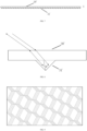
- FIG. 9 schematically shows a top view of distribution of micro-structures on a retroreflective element according to an embodiment of the present invention, for better understanding of the distribution of the micro-structures.
- a plurality of micro-structures are sequentially distributed, closely adjacent to one another, and extend on the retroreflective element. It should be understood that, only a portion of the retroreflective element is shown in the diagram, and the micro-structures may be distributed throughout the retroreflective element in this manner.
- micro-structure shown in the diagram is a concave portion resembling a cuboid, it should be understood that, a shape of the micro-structure is not limited thereto, and may be any type of the micro-structure as described above.
- the retroreflective element still causes a certain offset between a reflection path and an incident path of the light; and meanwhile, due to a diffraction effect of the light, the reflected light will have a certain divergence angle.
- These two points are two core factors that affect definition of imaging in the air according to the present invention, and these two factors are also mutually constrained.
- a relationship among a diameter of the micro-structure, a dot pitch of a pixel array of the source image, and an optical path from the real image to the retroreflective element is specifically designed in the present invention.
- an observation distance for an observer to observe the formed real image increases as the optical path from the real image to the retroreflective element increases, and preferably, the two are substantially linearly related to each other.
- a picture width of the formed real image is preferably, for example, 1 to 2 times of the observation distance; and if the observer wants to obtain a sufficiently clear real image, then it is necessary for the number of observed pixel points to reach a certain value, for example, at least 1024 pixel points are present in each dimension; and thus, the dot pitch of the selected image source may be derived (the dot pitch of the image source determines a light spot size of the formed real image).
- the diameter of the micro-structure is set to be the same order of magnitude as the dot pitch of the image source, which is, preferably, about 1/5, 1/4, 1/3, 1/2 of, or equal to the dot pitch of the image source. Therefore, the optical path and the dot pitch of the light source (in case of a matrix light source) may be selected according to the observation distance of an actual application scenario, so as to further select the size of the micro-structure.
- a relatively suitable observation distance is about 5 m
- an imaging system with an optical path of 2 m or slightly longer may be selected, and a relatively suitable picture length of the real image is about 5 m, at which time, if a resolution of 1024 pixels is desired, a dot matrix image source having a dot pitch of about 5 mm may be used, and it may be derived by calculation that a preferred size of the micro-structure ranges from 0.6 mm to 4.4 mm, and more preferably, is about 1.7 mm.
- a relatively suitable observation distance is about 1 m or more
- an imaging system with an optical path of about 0.5 m may be selected, and a relatively suitable picture length of the real image is about 2 m; at which time, if a resolution of 1024 pixels is desired, a dot matrix image source having a dot pitch of about 2 mm may be used, and it may be derived by calculation that a preferred size of the micro-structure ranges from 0.43 mm to 1.57 mm, and more preferably, is about 0.82 mm.
- a relatively suitable observation distance is about 0.5 m or less
- an imaging system with an optical path of about 0.1 m may be selected, and a relatively suitable picture length of the real image is about 1 m; at which time, if a resolution of 1024 pixels is desired, a dot matrix image source having a dot pitch of about 0.5 mm may be used, and it may be derived by calculation that a preferred size of the micro-structure ranges from 0.16 mm to 0.84 mm, and more preferably, is about 0.37 mm.
- the retroreflective element still causes a certain offset between a reflection path and an incident path of the light; and meanwhile, because of a diffraction effect of the light, the reflected light will have a certain divergence angle.
- An effect of light offset on the light spot size does not vary with an imaging distance, but varies linearly with a scale of the micro-structure. Therefore, it can be solved by using a method of reducing the size of a micro-structure unit, for example, ultra-fine processing, etc.
- a size of a spot caused by diffraction varies linearly with variation of the imaging distance, so it is a key factor to try to reduce light divergence caused by diffraction.
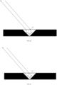
- incident light is refracted by an upper surface, and is irradiated on the right-angled triangular pyramid of the retroreflective unit; then the light is reflected thereon, and at a same time, due to Fraunhofer diffraction, diverges at a certain angle. Thereafter, the light is refracted by the upper surface of the retroreflective element, to form reflected light having a principal axis whose direction is opposite to that of the incident light, but with a small amount of offset and a certain divergence angle.
- a base portion of a retroreflective unit is divided into two main portions.
- a convex lens structure is used for forming a convex lens array on an upper portion of the base portion, that is, a side facing the transflective mirror.
- a right-angled triangular pyramid structure is used for forming a right-angled triangular pyramid array on a lower portion of the base portion, that is, a side away from the transflective mirror.
- a transparent base material is used throughout the base portion. Meanwhile, a thickness of the base portion is designed such that the right-angled triangular pyramid structure of the lower portion is arrayed on a focal plane of the convex lens of the upper portion.
- a highly reflective material layer is plated on a lower surface of the base portion, that is, a lower surface, or say, an outer side of the right-angled triangular pyramid structure.
- the incident light is refracted by an upper surface of the base portion, that is, an upper surface, or say, an outer side of the convex lens structure, and then is irradiated on the right-angled triangular pyramid; the light is reflected many times by the lower surface thereof, and at a same time, due to Fraunhofer diffraction, diverges at a certain angle; and thereafter, the light is refracted again on the upper surface of the retroreflective element.
- the refraction allows the light with a certain divergence angle to concentrate, and emit in a form of approximately parallel light.
- divergence caused by diffraction is reduced, and the spot size caused by diffraction can also be reduced even when the imaging distance is relatively long.
- each convex lens structure in the convex lens array has a diameter of about 1 mm, preferably less than 1 mm; and each right-angled triangular pyramid structure in the right-angled triangular pyramid array has an equilateral right-angled triangular pyramid structure, whose bottom face is an equilateral triangle; the bottom face has a side length of about 0.02 mm, and preferably less than 0.02 mm.
- one convex lens structure corresponds to dozens of right-angled triangular pyramid structures; however, a case where one convex lens structure corresponds to one right-angled triangular pyramid structure may also be taken into consideration.
- reflectance of a reflective material layer plated on the lower surface of the base portion is as high as 60%, and preferably, as high as 70%, 80% or 90%.
- the upper surface of the base portion is further plated with an anti-reflective material, such that transmittance of the surface is as high as 70%, and more preferably, as high as 80% or 90%.
- L 0 is the luminance of the image source
- T g and R g are respectively transmittance and reflectance of the transflective mirror
- ⁇ is a reflection luminous efficacy of the retroreflective element.
- a luminous efficacy of the transflective mirror is less than or equal to 1/4.
- FIG. 12 shows one embodiment of an imaging system for improving imaging luminance according to the technology.
- the system comprises an image source 1, a transflective mirror 2 and a retroreflective element 3.
- a plane where the transflective mirror 2 is located divides space into a first half region I and a second half region II, and both the image source 1 and the retroreflective element 3 are located in the first half region I.
- Light emitted by the image source 1 is reflected by the transflective mirror 2 and is irradiated on the retroreflective element 3, and then the light is retroreflected on the retroreflective element 3, so that reflected light and incident light on the retroreflective element 3 are located in the same path, but in opposite directions. Therefore, the light is reflected by the retroreflective element 3 and then emerges along an original incident path (of course, as observed microscopically, a reflection path may be considered to be slightly offset from an incident path; however, as observed macroscopically, the two paths may be considered to coincide completely), and after being transmitted by the transflective mirror, then forms a real image 4 in the second half region II.
- the image source 1 is an s-polarized light source; a selective transmissive film is plated on a side of the transflective mirror 2 that faces the image source 1, and the selective transmissive film is set to have higher reflectance with respect to s-polarized light, and higher transmittance with respect to p-polarized light.
- the selective transmissive film may be a single film layer, or may also be a plurality of film layers stacked.
- a component of the selective transmissive film is selected from special metal oxides, metal nitrides, metal oxynitride coatings, fluorides, and/or organic polymers; which may be one or more selected from the group consisting of tantalum pentoxide, titanium dioxide, magnesium oxide, zinc oxide, zirconium oxide, silicon dioxide, magnesium fluoride, silicon nitride, silicon oxynitride and aluminum fluoride.
- a side of the retroreflective element 3 that faces the transflective mirror 2 is further provided with a phase delay optical element 5, which is preferably a 1/4 wave plate, such that light of the s-polarized light source emitted from the transflective mirror 2 to the retroreflective element 3 becomes circularly polarized light after passing through the phase delay optical element 5.
- the circularly polarized light after being reflected by the retroreflective element 3, and then passing through the phase delay optical element 5, becomes the p-polarized light.
- Average reflectance of the selective transmissive film with respect to the s-polarized light is greater than 70%, preferably greater than 80%, or even greater than 90%; while average transmittance thereof with respect to the p-polarized light is greater than 70%, preferably greater than 80%, or even greater than 90%.
- the average reflectance of the selective transmissive film with respect to the s-polarized light is greater than 70%
- the average transmittance thereof with respect to the p-polarized light is also greater than 70% as an example.
- the result is nearly doubled as compared with the luminous efficacy of, for example, 25% in the above-described system. Then, the final imaging luminance is also nearly doubled.
- the image source 1 is selected to be an s-polarized light source emitting s-polarized light of a specific wavelength band
- the selective transmissive film is also set to have higher reflectance with respect to the s-polarized light of the specific wavelength band, and higher transmittance with respect to s-polarized light of other wavelength band and p-polarized light within a visible light band.
- average reflectance with respect to the s-polarized light of the specific wavelength band is greater than 80%, or even greater than 90%; while average transmittance with respect to s-polarized light of other wavelength band and p-polarized light within a visible light band is greater than 80%, or even greater than 90%.
- the specific wavelength band may be, for example, red light of 590 nm to 690 nm, green light of 500 nm to 565 nm, and blue light of 410 nm to 480 nm.
- the result is increased by nearly 1.6 times, as compared with the luminous efficacy of, for example, 25% in the above-described system. Then, the final imaging luminance is also increased by nearly 1.6 times.
- an anti-reflective film is further attached to a side of a transflective mirror 2 away from an image source 1, so as to increase light transmittance and improve a luminous efficacy.
- the anti-reflective film may increase the light transmittance by up to 3%, or even above 5%.
- the system comprises an image source 1, a transflective mirror 2 and a retroreflective element 3.
- a plane where the transflective mirror 2 is located divides space into a first half region I and a second half region II, the image source 1 is located in the first half region I, and the retroreflective element 3 is located in the second half region II.
- Light emitted by the image source 1 is irradiated on the retroreflective element 3 after being transmitted by the transflective mirror 2, and then the light is opposing reflected by the retroreflective element 3, so that reflected light and incident light on the retroreflective element 3 are located in the same path, but in opposite directions. Therefore, the light is reflected by the retroreflective element 3 and then emerges along an original incident path (of course, as observed microscopically, a reflection path may be considered to be slightly offset from an incident path; however, as observed macroscopically, the two paths may be considered to coincide completely), and after being reflected by the transflective mirror, then forms a real image 4 in the second half region II.
- the image source 1 adopts a p-polarized light source; a selective transmissive film is plated on a side of the transflective mirror 2 that faces the image source 1, and the selective transmissive film is set to have higher reflectance with respect to s-polarized light, and higher transmittance with respect to p-polarized light.
- the selective transmissive film may be a single film layer, or may also be a plurality of film layers stacked.
- a component of the selective transmissive film is selected from special metal oxides, metal nitrides, metal oxynitride coatings, fluorides, and/or organic polymers; which may be one or more selected from the group consisting of tantalum pentoxide, titanium dioxide, magnesium oxide, zinc oxide, zirconium oxide, silicon dioxide, magnesium fluoride, silicon nitride, silicon oxynitride and aluminum fluoride.
- a side of the retroreflective element 3 that faces the transflective mirror 2 is further provided with a phase delay optical element 5, which is preferably a 1/4 wave plate, such that light of the p-polarized light source emitted from the transflective mirror 2 to the retroreflective element 3 becomes circularly polarized light after passing through the phase delay optical element 5.
- the circularly polarized light after being reflected by the retroreflective element 3, and then passing through the phase delay optical element 5, becomes the s-polarized light.
- an anti-reflective film may also be used in the embodiment in FIG. 13 , so as to increase the light transmittance and improve the luminous efficacy.
- the anti-reflective film may increase the light transmittance by up to 3%, or even as high as 5%.
- the retroreflective element is divided into a plurality of small pieces (retroreflective sub-elements), which are discretely distributed on one side of the transflective mirror according to a certain rule, such that an included angle between incident light and a center line of a retroreflective unit is as small as possible, and an optical path from each of the retroreflective sub-elements to the real image is as short as possible, which is favorable for improving imaging luminance and definition.
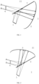
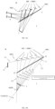
- FIG. 14a and FIG. 14b show an embodiment of an imaging system for improving imaging luminance and definition according to the technology.
- the system comprises: an image source 1, a transflective mirror 2 and a plurality of retroreflective sub-elements 300.
- a plane where the transflective mirror 2 is located divides space into a first half region I and a second half region II, and both the image source 1 and the retroreflective sub-elements 300 are located in the first half region I.
- the plurality of retroreflective sub-elements 300 form a retroreflective sub-element array 3000 (the reference sign 3000 and the reference sign 300 are noted in one position in the diagram for convenience).
- Light emitted by the image source 1 is irradiated on the retroreflective sub-element 300 after being reflected by the transflective mirror 2, and then the light is retroreflected by the retroreflective sub-element 300, so that reflected light and incident light on the retroreflective sub-element 300 are located in the same path, but in opposite directions. Therefore, the light is reflected by the retroreflective sub-element 300 and then emerges along an original incident path (of course, as observed microscopically, a reflection path may be considered to be slightly offset from an incident path; however, as observed macroscopically, the two paths may be considered to coincide completely), and after being transmitted by the transflective mirror, then forms a real image 4 in the second half region II.
- the retroreflective sub-element array 3000 includes an array first end 3001 and an array second end 3002. The array first end 3001 is closer to the transflective mirror 2 while the array second end 3002 is farther away from the transflective mirror 2.
- a reverse extension line of the vision domain boundary VDB1 intersects with the transflective mirror 2 at a transflective mirror first point 21 closer to the array first end 3001, while a reverse extension line of the vision domain boundary VDB2 intersects with the transflective mirror 2 at a transflective mirror second point 22 farther away from the array first end 3001.
- light emitted by the image source 1 has an Effective Exposure Region (EED) located between the image source 1 and the transflective mirror 2, the effective exposure region EED includes a first boundary L1 and a second boundary L2.
- the first boundary L1 is a connection line at a largest included angle to the transflective mirror 2 among connection lines from the transflective mirror first point 21 to respective light-emitting points of the image source 1
- the second boundary L2 is a connection line at a smallest included angle to the transflective mirror 2 among connection lines from the transflective mirror second point 22 to respective light-emitting points of the image source 1.
- each of the retroreflective sub-elements 300 includes a substantially planar base material, and a large number of retroreflective units (not shown) having a reflecting surface distributed on the base material.
- the retroreflective unit has a right-angled vertex micro-structure, the right-angled vertex micro-structure has at least one right-angled vertex, and three edges of the right-angled vertex are at right angles to one another.
- a straight line passing through the right-angled vertex and having equal included angles (each of which is about 54.7°) to the three edges of the right-angled vertex micro-structure is defined as a center line of the right-angled vertex micro-structure.
- an included angle between a center line of a right-angled vertex micro-structure and a normal of a base material plane is required to be as small as possible, which is, for example, less than 15°, less than 10°, less than 5°, or even 0°.
- each of the retroreflective sub-elements 300 includes a sub-element first end 301 and a sub-element second end 302.
- the sub-element first end 301 located above while the sub-element second end 302 is located below, so that the sub-element 300 is set vertically, or preferably, at a certain angle to a vertical direction.
- an angle of the retroreflective sub-element 300 to the vertical direction is adjusted such that an included angle between a connection line from a geometric center 303 (with reference to the partially enlarged portion in FIG. 14b ) of the retroreflective sub-element 300 to the vision domain point VDP and a center line of the right-angled vertex micro-structure on the retroreflective sub-element 300 is less than 15 degrees, preferably less than 10°, more preferably less than 5°, and most preferably, 0°; and thus, a reflected luminous efficacy is as high as possible.
- a retroreflective sub-element array 3000 is arranged such that each of the retroreflective sub-elements 300 does not shield light of the image source 1 that is emitted to the transflective mirror 2, which can ensure no imaging loss because the light from the image source 1 to the real image 4 is not shielded.
- each sub-element first end 301 and each sub-element second end 302 fall outside the effective exposure region EED, so that the light from the image source 1 to the real image 4 is not shielded. More preferably, each sub-element first end 301 falls on the first boundary L1, and each sub-element second end 302 falls outside the effective exposure region EED; which, thus, can further ensure that an optical path from the retroreflective sub-element 300 to the formed real image 4 is as short as possible.
- a retroreflective sub-element array 3000 is arranged such that reverse extension lines of all light rays forming a real image 4 can fall on a certain retroreflective sub-element 300, which, thus, can ensure no imaging loss because the light from the image source 1 to the real image 4 does not subjected to a reflection.
- all the retroreflective sub-elements 300 of the array 3000 are sequenced in a short-to-long order of a distance to the transflective mirror first point 21; a position of a retroreflective sub-element 300 having a shortest distance to the transflective mirror first point 21 is defined as the foremost, and a position of a retroreflective sub-element 300 having a longest distance to the transflective mirror first point 21 is defined as the last.
- connection line from a sub-element second end 302 of a former retroreflective sub-element 300 to the vision domain point VDP and the first boundary L1 form an intersection point
- a connection line from a sub-element first end 301 of a latter retroreflective sub-element 300 to the vision domain point VDP and the first boundary L1 also form an intersection point
- the former intersection point is located behind, or at least overlaps with the latter intersection point, which ensures all light rays emitted by the image source 1 that subject to a first reflection of the transflective mirror 2 to the array 3000 are reflected back in an opposite direction, without being missed.
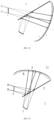
- FIG. 15a and FIG. 15b schematically show an imaging system for improving imaging luminance and definition according to another embodiment of the present invention.
- the system comprises an image source 1, a transflective mirror 2 and a plurality of retroreflective sub-elements 300.
- a plane where the transflective mirror 2 is located divides space into a first half region I and a second half region II, and the image source 1 is located in the first half region I, while the plurality of retroreflective sub-elements 300 are located in the second half region II.
- the plurality of retroreflective sub-elements 300 form a retroreflective sub-element array 3000 (the reference sign 3000 and the reference sign 300 are noted in one position in the diagram for convenience).
- Light emitted by the image source 1 is irradiated on the retroreflective sub-element 300 after being transmitted by the transflective mirror 2, and then the light is retroreflected by the retroreflective sub-element 300, so that reflected light and incident light on the retroreflective sub-element 300 are located in the same path, but in opposite directions. Therefore, the light is reflected by the retroreflective sub-element 300 and then emerges along an original incident path (of course, as observed microscopically, a reflection path may be considered to be slightly offset from an incident path; however, as observed macroscopically, the two paths may be considered to coincide completely), and after being reflected by the transflective mirror, then forms a real image 4 in the second half region II.
- the light emitted by the image source 1 is transmitted (rather than reflected) by the transflective mirror 2 and then reaches the retroreflective sub-element 300. While the light reflected by the retroreflective sub-element 300 is reflected (rather than transmitted) by the transflective mirror 2, and then forms the real image 4. The finally formed real image 4 and the retroreflective sub-element 300 are located in the same half region, rather than different half regions.
- the system in FIG. 15b also comprises a complete real image vision domain CRIVD, a vision domain point VDP, two vision domain boundaries VDB1 and VDB2 (not shown in FIG. 15b ); also comprises an effective exposure region EED, as well as a first boundary L1 and a second boundary L2; and further comprises an array first end 3001 and an array second end 3002 of the retroreflective sub-element array 3000, a transflective mirror first point 21 and a transflective mirror second point 22.
- the system in FIG. 14b is referred to for definitions of all these features. Configuration of the micro-structure in the system of FIG. 15b is also consistent with that according to the embodiment shown in FIG. 14b .
- a third boundary L3 is defined as a line that is mirror-symmetrical to the first boundary L1 with respect to the transflective mirror 2
- an effective imaging region EID is defined as a region that is mirror-symmetrical to the effective exposure region EED with respect to the transflective mirror 2
- a virtual vision domain point VVDP is defined as a point that is mirror-symmetrical to the vision domain point VDP with respect to the transflective mirror 2.
- a sub-element first end 301 of each of the retroreflective sub-elements 300 is on the right (closer to the transflective mirror 2), and a sub-element second end 302 is on the left (farther away from the transflective mirror 2), so that the sub-element 300 is arranged horizontally, or preferably at a certain angle to a horizontal direction.
- an angle of the retroreflective sub-element 300 to the horizontal direction is adjusted such that an included angle between a connection line from a geometric center 303 of the retroreflective sub-element 300 to the virtual vision domain point VVDP and a center line of the right-angled vertex micro-structure on the retroreflective sub-element 300 is less than 15 degrees, preferably less than 10°, more preferably less than 5°, and most preferably, 0°; and thus, a reflected luminous efficacy is as high as possible.
- the retroreflective sub-element array 3000 is arranged such that respective retroreflective sub-elements 300 do not shield light of the image source 1 that is emitted to the transflective mirror 2, which, thus, can ensure no imaging loss because the light from the image source 1 to the real image 4 is not shielded.
- each sub-element first end 301 and each sub-element second end 302 fall outside the effective imaging region EID, so that the light from the image source 1 to the real image 4 is not shielded. More preferably, each sub-element first end 301 falls on the first boundary L1, and each sub-element second end 302 falls outside the effective imaging region EID; which, thus, can further ensure that the optical path from the retroreflective sub-element 300 to the real image 4 is as short as possible.
- the retroreflective sub-element array 3000 is arranged such that extension lines of all light rays emitted by the image source 1 within the effective exposure region EED can fall on a certain retroreflective sub-element 300, which, thus, can ensure no imaging loss because the light from the image source 1 to the real image 4 does not escape a reflection.
- all the retroreflective sub-elements 300 of the array 3000 are sequenced in a short-to-long order of a distance to the transflective mirror first point 21; a position of a retroreflective sub-element 300 having a shortest distance to the transflective mirror first point 21 is defined as the foremost, and a position of a retroreflective sub-element 300 having a longest distance to the transflective mirror first point 21 is defined as the last.
- a connection line from a sub-element second end 302 of the former retroreflective sub-element 300 to a virtual vision domain point VVDP and a third boundary L3 form an intersection point
- a connection line from a sub-element first end 301 of the latter retroreflective sub-element 300 to the virtual vision domain point VVDP and the third boundary L3 also form an intersection point
- the former intersection point is located behind, or at least overlaps with the latter intersection point, which ensures all light rays emitted by the image source 1 that subject to a first transmittance of the transflective mirror 2 to the array 3000 are reflected back in an opposite direction, without being missed.
- the reflecting surface for example, the surface coated with the highly reflective coating
- the reflecting surface may also be considered as a portion attached onto the micro-structure.
- the retroreflective element may be divided into a large number of retroreflective units, each retroreflective unit includes a micro-structure having a reflecting surface; the micro-structure may be the spherical micro-structure or the right-angled vertex micro-structure as described above.
- the reflecting surface may even be described as an independent structural unit.
- each retroreflective unit includes a reflecting surface, and the reflecting surface may be attached onto at least one of the first material and the second material thereon; and the reflecting surface may be formed by one or more faces of the above-described micro-structure.
- an image may be formed directly in the air, or even in vacuum, neither with the help of an auxiliary device such as a helmet, nor with the help of an imaging screen or a particulate medium in the air. It is a real technology of imaging in the air.
- the image formed is suspended in the air, so a large number of interactions and applications may be developed, which is of epoch-making significance.
Landscapes
- Physics & Mathematics (AREA)
- General Physics & Mathematics (AREA)
- Optics & Photonics (AREA)
- Optical Elements Other Than Lenses (AREA)
- Lenses (AREA)
- Testing, Inspecting, Measuring Of Stereoscopic Televisions And Televisions (AREA)
Description
- The present invention claims priority of Chinese Patent Application No.
CN2016111240031 filed on December 8, 2016 CN2017112704019 filed on December 5, 2017 CN2017112712706 filed on December 5, 2017 CN2017112692670 filed on December 5, 2017 CN2017112712725 filed on December 5, 2017 - The present invention relates to the field of holographic imaging, and more particularly, to a system for imaging in air.
- A holographic technology is a technology of recording and reproducing a real three-dimensional image of an object on principles of interference and diffraction.
- In a traditional holographic imaging method, a holographic image is produced on a principle of laser interference. Light emitted by a laser source is split into two beams, of which one beam is directly emitted to a sensitometric strip, and the other beam is reflected by a photographed object and then emitted to the sensitometric strip. The two beams are superimposed on the sensitometric strip to cause interference; and finally, the reproduced hologram is further processed using a basic principle of digital images, to remove digital noise and obtain a clear holographic image. The method has disadvantages of high requirements for monochromaticity and difficulty in implementing color imaging.
- Existing holographic imaging technologies are generally classified into three types below.
- In a first type, it is necessary to have the aid of virtual reality or augmented reality glasses or helmets, such as Microsoft's HoloLens, etc.; and such type of technology has limited application scenarios and is currently expensive due to the need for auxiliary devices.
- In a second type, a high-speed rotating reflective plate and a high-speed refresh projector are required to project an image onto the high-speed rotating reflective plate, so as to achieve a three-dimensional image. A rotary holographic projection show cabinet by using such type of technology is disclosed in a patent document No.
CN105372926A . The technology is difficult to realize interaction, and has a strict demand on a site space. - In a third type, with the help of a medium containing fine particles, for example, the air containing water vapor, an image is projected onto a small water droplet formed by liquefaction of the water vapor, so that an image having a strong hierarchical and stereoscopic sense may be formed, due to unbalanced molecular vibration. Application of such type of technology is disclosed in patent documents No.
CN104977794A and No.CN 103116422A , in both of which a water vapor curtain wall is used for forming an image in the air. But auxiliary tools for producing the water vapor curtain wall are still required for application of the technology, so it is not very convenient to use. - In general, in the above-described technologies, the image is either formed on a virtual reality or augmented reality tool, or formed on a high-speed rotating reflective plate, or formed on vapor particles in the air, none of which is really imaging in the air.
US 6147805 discloses a head mounted display system including focusing optics to focus light from an image source, retro-reflector and beamsplitter.US 2015248014 discloses a retro-imaging system. A polarization beam splitter layer and a retarder layer placed in front of the retro-reflector array may be oriented such that polarized light is used as source, source input light is efficiently reflected at the polarization beam splitter layer toward the retro-reflective layer, and polarization is converted to circular upon first pass through retarder layer.US 2014055858 A discloses a retroreflective article. The retroreflective article includes a first transparent layer having a back surface with retroreflective prisms, and a planar front surface that has an index of refraction n1. - It is an object of the present invention to provide a system for imaging in air.
- The object is achieved by the features of the respective independent claims. Further embodiments are defined in the corresponding dependent claims.
- In order to clearly illustrate the technical solution of the embodiments of the present invention or the prior art, the drawings used in description of the embodiments or the prior art will be briefly introduced in the following. It is obvious that the described drawings are just a part of the embodiments of the present invention. These drawings are merely exemplary and not limitative with respect to the present invention.
-
FIG. 1 schematically shows an imaging system according to an embodiment of the present invention not falling within the scope of the claims; -
FIG. 2 schematically shows an imaging system according to another embodiment of the present invention not falling within the scope of the claims; -
FIG. 3 schematically shows a retroreflective element according to an embodiment of the present invention not falling within the scope of the claims; -
FIG. 4 schematically shows a schematic diagram of a micro-structure of a retroreflective element and a retroreflection path according to an embodiment of the present invention not falling within the scope of the claims; -
FIG. 5 schematically shows a retroreflective element according to another embodiment of the present invention; -
FIG. 6A ,FIG. 6B and FIG. 6C schematically show schematic diagrams of a micro-structure of a retroreflective element and a retroreflection path according to another embodiment of the present invention; -
FIG. 7 schematically shows a retroreflective element according to still another embodiment of the present invention; -
FIG. 8 schematically shows a schematic diagram of a micro-structure of a retroreflective element and a retroreflection path according to still another embodiment of the present invention; -
FIG. 9 schematically shows a top view of distribution of micro-structures of a retroreflective element according to an embodiment of the present invention; -
FIG. 10 shows a schematic diagram of a light path upon a right-angled triangular pyramid structure being used as a retroreflective unit according to an embodiment of the present invention; -
FIG. 11 shows a schematic diagram of a light path upon a combination of a right-angled triangular pyramid structure and a convex lens structure being used as a retroreflective unit according to an embodiment of the present invention; -
FIG. 12 schematically shows an imaging system for improving imaging luminance according to an embodiment of the present invention; -
FIG. 13 schematically shows an imaging system for improving imaging luminance according to another embodiment of the present invention; -
FIG. 14a and FIG. 14b schematically show an imaging system for improving imaging luminance and definition according to an embodiment of the present invention; and -
FIG. 15a and FIG. 15b schematically show an imaging system for improving imaging luminance and definition according to another embodiment of the present invention. - In order to make objects, technical details and advantages of the present invention apparent, hereinafter, the present invention will be further described in detail in connection with the drawings.
- For concise and intuitive descriptions, technical solutions of the present invention are described below using representative embodiments. A large quantity of details in the embodiments is merely used for helping understand the solutions of the present invention. However, apparently, when being implemented, technical solutions of the present invention may not be limited to these details. To avoid unnecessarily blurring the solutions of the present invention, some embodiments are not described in great detail, only with frames provided. In the following text, the term "include" refers to "include but is not limited to", and the term "according to..." refers to "according to at least..., but not being limited only to according to...". "First", "second", etc. are used merely for referring to a feature, and are not intended to impose any limitation on the feature, for example, a limitation in the order. Due to Chinese language habits, when a quantity of components is not particularly pointed out, this means that there may be one or more components, or may be understood as at least one component.
-
FIG. 1 shows an imaging system according to an embodiment of the present invention. As shown in the diagram, the system comprises animage source 1, atransflective mirror 2 and aretroreflective element 3. A plane where thetransflective mirror 2 is located divides space into a first half region I and a second half region II, and both theimage source 1 and theretroreflective element 3 are located in the first half region I. The embodiment described in this paragraph is to be considered merely as an example suitable for understanding the invention. - Light emitted by the
image source 1 is irradiated on theretroreflective element 3 after being reflected by thetransflective mirror 2, and then the light is retroreflected by theretroreflective element 3, so that reflected light and incident light on theretroreflective element 3 are located in the same path, but in opposite directions. Therefore, the light is reflected by theretroreflective element 3 and then emerges along an original incident path (of course, as observed microscopically, a reflection path may be considered to be slightly offset from an incident path; however, as observed macroscopically, the two paths may be considered to coincide completely), and after being transmitted by the transflective mirror, then forms areal image 4 in the second half region II. - The
image source 1 may be a display imaging device, or may also be a virtual image or a real image formed by such a display imaging device. - For example, the display imaging device may be a liquid crystal screen, and a backlight source of the liquid crystal screen includes one or more selected from the group consisting of a laser, light emitting diode, an organic light-emitting diode, an stimulated fluorescence luminescence material and a quantum dot excitation light source; the display imaging device may also be an active luminous dot matrix screen composed of light-emitting point light source such as an LED, an OLED and a plasma light-emitting point; the display imaging device may also be a projection imaging system based on a projection technology, for example, DLP, LCOS and LCD, etc., which, as driven by light source such as an LED, an OLED, a laser, a fluorescent, or a combination thereof, causes light to be reflected or transmitted by a DMD, an LCOS and an LCD, etc., and then projected by a projection lens on a projection screen to form an image; or the display imaging device may also be a projection imaging system in which a laser beam scans on a screen to form an image. Moreover, with respect to all the above-described display imaging devices, a real image or a virtual image formed by a single or multiple refractions or reflections may also be used as an image source.
- The
image source 1 may be a stereo image source. The stereo image source includes a three-dimensional stereoscopic display device which can display a three-dimensional stereo image, structure and video source. The three-dimensional stereoscopic display device usually includes a control module and a high-speed projection module or a high-speed display module. The control module controls the projection module or the display module to project or display a series of two-dimensional image slices onto a plurality of optical flats at a high speed, so that an observer observes a three-dimensional image, structure or video. The three-dimensional stereoscopic display device includes a translational scanning imaging system or a rotational scanning imaging system, ect. - The transflective mirror may be made of various suitable transparent materials, for example, a PC resin, a PET resin, a PMMA resin, glass, quartz, and the like. Transmittance of the transflective mirror ranges from 20% to 80%; preferably, is about 50%. Reflectance of the transflective mirror also ranges from 20% to 80%; preferably, is also about 50%.
- The
retroreflective element 3 is preferably a thin film, a curtain, a sheet or a resin which has micro-structures distributed thereon. Theretroreflective element 3 preferably has a certain curvature and is curved toward the transflective mirror, so as to increase imaging luminance. Theretroreflective element 3 will be described in detail below. - With reference to
FIG. 2 , in another embodiment of the present invention, a system comprises animage source 1, atransflective mirror 2 and aretroreflective element 3. A plane where thetransflective mirror 2 is located divides space into a first half region I and a second half region II, theimage source 1 is located in the first half region I, and theretroreflective element 3 is located in the second half region II. The embodiment described in this paragraph is to be considered merely as an example suitable for understanding the invention. - Light emitted by the
image source 1 is irradiated on theretroreflective element 3 after being transmitted by thetransflective mirror 2, and then the light is reflected by theretroreflective element 3, so that reflected light and incident light on theretroreflective element 3 are located in the same path, but in opposite directions. Therefore, the light is reflected by theretroreflective element 3 and then emerges along an original incident path, and then forms areal image 4 in the second half region II after being reflected by the transflective mirror. - Of course, it should be understood that, because the light has wave-particle duality, when the light is reflected from the
retroreflective element 3, there will be a certain diffraction effect, and the reflected light will have a certain divergence angle; understanding from the perspective, as long as a principal axis of the reflected light has a direction opposite to that of the incident light, the meaning of "retroreflection" in the present invention is also satisfied. - In this embodiment, the light emitted by the
image source 1 is transmitted (rather than reflected) by thetransflective mirror 2 and then reaches theretroreflective element 3. While the light reflected by theretroreflective element 3 is further reflected (rather than transmitted) by thetransflective mirror 2, and then forms thereal image 4. The finally formedreal image 4 and theretroreflective element 3 are located in the same half region, rather than different half regions. The embodiment described in this paragraph is to be considered merely as an example suitable for understanding the invention. - In still another embodiment of the present invention (not shown), the above-described two embodiments are combined. Two retroreflective elements are used, such that light emitted by an image source is reflected by a transflective mirror and then reaches one of the retroreflective elements, while the light reflected by the retroreflective element is further transmitted by the transflective mirror, and then forms a real image; and the light emitted by the image source is transmitted by the transflective mirror and then reaches the other retroreflective element, while the light reflected by the other retroreflective element further is reflected by the transflective mirror, and then forms a real image. In this way, the two real images generated completely overlap with each other, resulting in imaging of stronger luminance. The embodiment described in this paragraph is to be considered merely as an example suitable for understanding the invention.
- Of course, it should be understood that, in other embodiments, additionally or alternatively, two image sources may be used. At this time, it is necessary to adjust positions of the two image sources as well as a transflective mirror and a retroreflective element, so that the finally formed real images completely overlap with each other in space.
- The retroreflective element in the present invention is a specially treated element, which includes, for example, a base material coated with a highly reflective coating, and, for example, retroreflective micro-structures evenly distributed on the base material. Reflectance of the highly reflective coating is as high as 60%, preferably, as high as 70%, 80% or 90%. It should be understood that, the highly reflective coating may also be attached onto the base material in other modes, for example, plating.
- Of course, the highly reflective coating may be attached, for example, onto a face of the micro-structure that faces the base material, or onto a region where the micro-structure borders the base material.
- It should be understood that, distribution of the retroreflective micro-structures on the base material may also be uneven, even distribution may achieve a better imaging effect; however, some deliberately arranged uneven distributions may be used for special imaging purposes.
- With reference to
FIG. 3 , a retroreflective element according to one embodiment of the present invention is shown. Theretroreflective element 3 includes a thin film or a curtain used as abase material 30. Thebase material 30 is coated with a highly reflective coating. Further, spherical micro-structures 31 are evenly distributed on thebase material 30. The embodiment described in this paragraph is to be considered merely as an example suitable for understanding the invention. - With reference to
FIG. 4 , an enlarged view of the spherical micro-structure and a schematic diagram of a retroreflection path are shown. The embodiment described in this paragraph is to be considered merely as an example suitable for understanding the invention. - Light from a transflective mirror is refracted by an upper surface of the
spherical micro-structure 31, and then is irradiated on the highly reflective coating of thebase material 30; after being reflected, the light is emitted back to the upper surface of thespherical micro-structure 31; and after being subjected to another refraction, the light is emitted to the transflective mirror. The structure of thespherical micro-structure 31 allows the light to return to the transflective mirror almost along the original path (as described above, as observed macroscopically, it may be considered that the light returns along the original path). - According to the invention, with reference to
FIG. 5 , a retroreflective element according to another embodiment of the present invention is shown. Abase material 30 of theretroreflective element 3 further has right-angled vertex micro-structures 31' evenly distributed thereon. The right-angled vertex micro-structure 31' may be a transparent micro-structure body having at least one vertex whose three edges are at right angles to one another, that is embedded in thebase material 30, for example, a micro-cube or a micro-cuboid, or a portion of at least one vertex thereof. The at least one vertex is definitely embedded in the base material 30 (with reference toFIG. 6A ). In some embodiments, a right-angled vertex micro-structure 31' is a micro-triangular pyramid whose three edges are at right angles to one another, and a vertex is embedded in the base material 30 (with reference toFIG. 6B ); preferably, a bottom face opposite to the vertex is flush with thebase material 30; and more preferably, an anti-reflective film is attached onto the bottom face. In a more preferred embodiment, an included angle between at least one face of the three faces formed by the three edges and the bottom face is less than 54 degrees. - It should be understood that, the three edges may be equal in length, or may also be unequal in length. A length of the edge may be selected between 20 micrometers and 5 millimeters. Preferably, among the three edges, a length of a longest edge does not exceed 10 times of the length of a shortest edge.
- It should be further understood that, the three faces formed by the three edges should also be perpendicular to one another, that is, a dihedral angle between any two of the three faces should be 90 degrees. However, due to constraints of a process, even if these dihedral angles are not exactly 90 degrees, they can also satisfy requirements of the present invention as long as their errors are within an allowable error range for machining, for example, ±2 minutes.
- In another embodiment, the right-angled vertex micro-structure 31' may be a concave portion formed by imprinting a portion of one vertex of the above-described micro-structure body onto the base material 30 (with reference to
FIG. 6C ). - According to the invention,
FIG. 6A ,FIG. 6B and FIG. 6C show enlarged views of the right-angled vertex micro-structures inFIG. 5 and schematic diagrams of retroreflection paths. In the embodiment shown inFIG. 6A andFIG. 6B , the right-angled vertex micro-structure 31' is a transparent micro-structure body. Light from a transflective mirror is refracted by an incident surface (for example, an upper surface) of the right-angled vertex micro-structure 31' and is irradiated on a highly reflective coating of a thin film orcurtain 30; after being subjected to three reflections, the light is emitted back to an emergent surface (for example, the upper surface) of the right-angled vertex micro-structure 31'; thereafter, the light is retroreflected again, and then is emitted to the transflective mirror. In the embodiment shown inFIG. 6C , the right-angled vertex micro-structure 31' is a concave portion; after being subjected to a transmission or a reflection of the transflective mirror, the light is directly incident on the concave portion, and after being subjected to three reflections, the light is emitted to the transflective mirror. The structure of the right-angled vertex micro-structure 31' allows the light to return to the transflective mirror almost along the original path (similarly, as observed macroscopically, it may be considered that the light returns along the original path). - According to the invention,
FIG. 7 shows a retroreflective element according to yet another embodiment of the present invention. A base material 30' of theretroreflective element 3 further has right-angled vertex micro-structures 31' evenly distributed thereon. The base material 30' itself is a transparent base material, and the right-angled vertex micro-structure 31' is also a transparent micro-structure body. Those faces of the right-angled vertex micro-structure 31' away from the base material 30' are coated with a highly reflective coating. - The right-angled vertex micro-structure 31' is preferably formed integrally with the base material 30'; or certainly they may also be separately formed and then the right-angled vertex micro-structure is attached onto the base material 30'. Preferably, the base material 30' and the right-angled vertex micro-structure 31' are made of the same material, or at least have the same refractive index.
- According to the invention,
FIG. 8 shows an enlarged view of the right-angled vertex micro-structure inFIG. 7 and a schematic diagram of a retroreflection path. Light from a transflective mirror is refracted by an upper surface of the base material 30' and is irradiated on a highly reflective coating of the right-angled vertex micro-structure 31'; after being subjected to three reflections, the light is emitted back to the upper surface of the base material 30'; and after being subjected to another refraction, the light is emitted to the transflective mirror. The structure of the right-angled vertex micro-structure 31' allows the light to return to the transflective mirror almost along the original path (as described above, as observed macroscopically, it may be considered that the light returns along the original path). - According to the invention,
FIG. 9 schematically shows a top view of distribution of micro-structures on a retroreflective element according to an embodiment of the present invention, for better understanding of the distribution of the micro-structures. As shown in the diagram, a plurality of micro-structures are sequentially distributed, closely adjacent to one another, and extend on the retroreflective element. It should be understood that, only a portion of the retroreflective element is shown in the diagram, and the micro-structures may be distributed throughout the retroreflective element in this manner. In addition, although the micro-structure shown in the diagram is a concave portion resembling a cuboid, it should be understood that, a shape of the micro-structure is not limited thereto, and may be any type of the micro-structure as described above. - As described above, microscopically, the retroreflective element still causes a certain offset between a reflection path and an incident path of the light; and meanwhile, due to a diffraction effect of the light, the reflected light will have a certain divergence angle. These two points are two core factors that affect definition of imaging in the air according to the present invention, and these two factors are also mutually constrained. The smaller the size of the micro-structure of the retroreflective element, the smaller a light offset caused thereby, but the larger a light spot caused by diffraction; on the contrary, the larger the size of the micro-structure, the smaller the light spot caused by diffraction, but the larger the light offset caused thereby. In order to overcome adverse effects of these two mutually constrained relationships on imaging definition, a relationship among a diameter of the micro-structure, a dot pitch of a pixel array of the source image, and an optical path from the real image to the retroreflective element is specifically designed in the present invention.
- In general, an observation distance for an observer to observe the formed real image increases as the optical path from the real image to the retroreflective element increases, and preferably, the two are substantially linearly related to each other. For the observer, in consideration of a comfortable viewing angle, a picture width of the formed real image is preferably, for example, 1 to 2 times of the observation distance; and if the observer wants to obtain a sufficiently clear real image, then it is necessary for the number of observed pixel points to reach a certain value, for example, at least 1024 pixel points are present in each dimension; and thus, the dot pitch of the selected image source may be derived (the dot pitch of the image source determines a light spot size of the formed real image). In consideration of a visual effect of imaging in the air, in the present invention, the diameter of the micro-structure is set to be the same order of magnitude as the dot pitch of the image source, which is, preferably, about 1/5, 1/4, 1/3, 1/2 of, or equal to the dot pitch of the image source. Therefore, the optical path and the dot pitch of the light source (in case of a matrix light source) may be selected according to the observation distance of an actual application scenario, so as to further select the size of the micro-structure.
- In one example, in case of an application scenario of, for example, a large advertisement display, etc., a relatively suitable observation distance is about 5 m, an imaging system with an optical path of 2 m or slightly longer may be selected, and a relatively suitable picture length of the real image is about 5 m, at which time, if a resolution of 1024 pixels is desired, a dot matrix image source having a dot pitch of about 5 mm may be used, and it may be derived by calculation that a preferred size of the micro-structure ranges from 0.6 mm to 4.4 mm, and more preferably, is about 1.7 mm.
- In another example, in case of an application scenario of, for example, a general-size advertisement display, etc., a relatively suitable observation distance is about 1 m or more, an imaging system with an optical path of about 0.5 m may be selected, and a relatively suitable picture length of the real image is about 2 m; at which time, if a resolution of 1024 pixels is desired, a dot matrix image source having a dot pitch of about 2 mm may be used, and it may be derived by calculation that a preferred size of the micro-structure ranges from 0.43 mm to 1.57 mm, and more preferably, is about 0.82 mm.
- In still another example, in case of an application scenario of, for example, a close-range or small-size display, etc., a relatively suitable observation distance is about 0.5 m or less, an imaging system with an optical path of about 0.1 m may be selected, and a relatively suitable picture length of the real image is about 1 m; at which time, if a resolution of 1024 pixels is desired, a dot matrix image source having a dot pitch of about 0.5 mm may be used, and it may be derived by calculation that a preferred size of the micro-structure ranges from 0.16 mm to 0.84 mm, and more preferably, is about 0.37 mm.
- As described above, microscopically, the retroreflective element still causes a certain offset between a reflection path and an incident path of the light; and meanwhile, because of a diffraction effect of the light, the reflected light will have a certain divergence angle. An effect of light offset on the light spot size does not vary with an imaging distance, but varies linearly with a scale of the micro-structure. Therefore, it can be solved by using a method of reducing the size of a micro-structure unit, for example, ultra-fine processing, etc. A size of a spot caused by diffraction varies linearly with variation of the imaging distance, so it is a key factor to try to reduce light divergence caused by diffraction.
- According to the invention, as schematically shown in
FIG. 10 , upon a right-angled triangular pyramid structure being used as a retroreflective unit, incident light is refracted by an upper surface, and is irradiated on the right-angled triangular pyramid of the retroreflective unit; then the light is reflected thereon, and at a same time, due to Fraunhofer diffraction, diverges at a certain angle. Thereafter, the light is refracted by the upper surface of the retroreflective element, to form reflected light having a principal axis whose direction is opposite to that of the incident light, but with a small amount of offset and a certain divergence angle. - In order to minimize the adverse effect of light divergence caused by diffraction on imaging definition, a new design for the retroreflective unit is proposed in the present invention to reduce divergence caused by diffraction.
- According to the invention, as shown in
FIG. 11 , in one embodiment, a base portion of a retroreflective unit is divided into two main portions. A convex lens structure is used for forming a convex lens array on an upper portion of the base portion, that is, a side facing the transflective mirror. While a right-angled triangular pyramid structure is used for forming a right-angled triangular pyramid array on a lower portion of the base portion, that is, a side away from the transflective mirror. A transparent base material is used throughout the base portion. Meanwhile, a thickness of the base portion is designed such that the right-angled triangular pyramid structure of the lower portion is arrayed on a focal plane of the convex lens of the upper portion. - A highly reflective material layer is plated on a lower surface of the base portion, that is, a lower surface, or say, an outer side of the right-angled triangular pyramid structure. Thus, the incident light is refracted by an upper surface of the base portion, that is, an upper surface, or say, an outer side of the convex lens structure, and then is irradiated on the right-angled triangular pyramid; the light is reflected many times by the lower surface thereof, and at a same time, due to Fraunhofer diffraction, diverges at a certain angle; and thereafter, the light is refracted again on the upper surface of the retroreflective element. On a focusing principle of the convex lens, the refraction allows the light with a certain divergence angle to concentrate, and emit in a form of approximately parallel light. Thus, divergence caused by diffraction is reduced, and the spot size caused by diffraction can also be reduced even when the imaging distance is relatively long.
- In this embodiment, each convex lens structure in the convex lens array has a diameter of about 1 mm, preferably less than 1 mm; and each right-angled triangular pyramid structure in the right-angled triangular pyramid array has an equilateral right-angled triangular pyramid structure, whose bottom face is an equilateral triangle; the bottom face has a side length of about 0.02 mm, and preferably less than 0.02 mm. In general, one convex lens structure corresponds to dozens of right-angled triangular pyramid structures; however, a case where one convex lens structure corresponds to one right-angled triangular pyramid structure may also be taken into consideration.
- In this embodiment, reflectance of a reflective material layer plated on the lower surface of the base portion is as high as 60%, and preferably, as high as 70%, 80% or 90%.
- In a preferred embodiment, the upper surface of the base portion is further plated with an anti-reflective material, such that transmittance of the surface is as high as 70%, and more preferably, as high as 80% or 90%.
- As described above, in the system for imaging in the air shown in
FIG. 1 and FIG. 2 , it is necessary for the light emitted by the image source to be subjected to a reflection and a transmission (regardless of order) of the transflective mirror, as well as a reflection of the retroreflective element, so as to form an image. An approximate calculation formula of final imaging luminance L is:

- L 0 is the luminance of the image source, Tg and Rg are respectively transmittance and reflectance of the transflective mirror, and η is a reflection luminous efficacy of the retroreflective element.
- With respect to a conventional transflective mirror, regardless of absorption of light energy by the base material, there is an approximate relationship as follows:
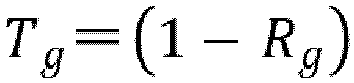
- Then

- Thus, it can be derived that, a luminous efficacy of the transflective mirror is less than or equal to 1/4.
- In order to improve the imaging luminance, the present invention further provides a technology for improving the luminous efficacy and enhancing the imaging luminance. According to the invention,
FIG. 12 shows one embodiment of an imaging system for improving imaging luminance according to the technology. - Similar to the embodiment shown in
FIG. 1 , the system comprises animage source 1, atransflective mirror 2 and aretroreflective element 3. A plane where thetransflective mirror 2 is located divides space into a first half region I and a second half region II, and both theimage source 1 and theretroreflective element 3 are located in the first half region I. - Light emitted by the
image source 1 is reflected by thetransflective mirror 2 and is irradiated on theretroreflective element 3, and then the light is retroreflected on theretroreflective element 3, so that reflected light and incident light on theretroreflective element 3 are located in the same path, but in opposite directions. Therefore, the light is reflected by theretroreflective element 3 and then emerges along an original incident path (of course, as observed microscopically, a reflection path may be considered to be slightly offset from an incident path; however, as observed macroscopically, the two paths may be considered to coincide completely), and after being transmitted by the transflective mirror, then forms areal image 4 in the second half region II. - The
image source 1 is an s-polarized light source; a selective transmissive film is plated on a side of thetransflective mirror 2 that faces theimage source 1, and the selective transmissive film is set to have higher reflectance with respect to s-polarized light, and higher transmittance with respect to p-polarized light. The selective transmissive film may be a single film layer, or may also be a plurality of film layers stacked. A component of the selective transmissive film is selected from special metal oxides, metal nitrides, metal oxynitride coatings, fluorides, and/or organic polymers; which may be one or more selected from the group consisting of tantalum pentoxide, titanium dioxide, magnesium oxide, zinc oxide, zirconium oxide, silicon dioxide, magnesium fluoride, silicon nitride, silicon oxynitride and aluminum fluoride. - As shown in
FIG. 12 , a side of theretroreflective element 3 that faces thetransflective mirror 2 is further provided with a phase delayoptical element 5, which is preferably a 1/4 wave plate, such that light of the s-polarized light source emitted from thetransflective mirror 2 to theretroreflective element 3 becomes circularly polarized light after passing through the phase delayoptical element 5. The circularly polarized light, after being reflected by theretroreflective element 3, and then passing through the phase delayoptical element 5, becomes the p-polarized light. - Average reflectance of the selective transmissive film with respect to the s-polarized light is greater than 70%, preferably greater than 80%, or even greater than 90%; while average transmittance thereof with respect to the p-polarized light is greater than 70%, preferably greater than 80%, or even greater than 90%.
- With a case where the average reflectance of the selective transmissive film with respect to the s-polarized light is greater than 70%, while the average transmittance thereof with respect to the p-polarized light is also greater than 70% as an example. In a case that the light passes through the transflective mirror, its luminous efficacy should be greater than:

- The result is nearly doubled as compared with the luminous efficacy of, for example, 25% in the above-described system. Then, the final imaging luminance is also nearly doubled.
- In a preferred embodiment, the
image source 1 is selected to be an s-polarized light source emitting s-polarized light of a specific wavelength band, and the selective transmissive film is also set to have higher reflectance with respect to the s-polarized light of the specific wavelength band, and higher transmittance with respect to s-polarized light of other wavelength band and p-polarized light within a visible light band. For example, average reflectance with respect to the s-polarized light of the specific wavelength band is greater than 80%, or even greater than 90%; while average transmittance with respect to s-polarized light of other wavelength band and p-polarized light within a visible light band is greater than 80%, or even greater than 90%. The specific wavelength band may be, for example, red light of 590 nm to 690 nm, green light of 500 nm to 565 nm, and blue light of 410 nm to 480 nm. - With a case where the average reflectance of the selective transmissive film with respect to the s-polarized light of the specific wavelength band is greater than 80%, while the average transmittance with respect to p-polarized light within a visible light band is greater than 80% as an example. When the light passes through the transflective mirror, its luminous efficacy should be greater than:

- The result is increased by nearly 1.6 times, as compared with the luminous efficacy of, for example, 25% in the above-described system. Then, the final imaging luminance is also increased by nearly 1.6 times.
- In another preferred embodiment, an anti-reflective film is further attached to a side of a
transflective mirror 2 away from animage source 1, so as to increase light transmittance and improve a luminous efficacy. Preferably, the anti-reflective film may increase the light transmittance by up to 3%, or even above 5%. - According to the invention,
FIG. 13 shows another embodiment of an imaging system for improving imaging luminance according to the technology. - Similar to the embodiment shown in
FIG. 2 , the system comprises animage source 1, atransflective mirror 2 and aretroreflective element 3. A plane where thetransflective mirror 2 is located divides space into a first half region I and a second half region II, theimage source 1 is located in the first half region I, and theretroreflective element 3 is located in the second half region II. - Light emitted by the
image source 1 is irradiated on theretroreflective element 3 after being transmitted by thetransflective mirror 2, and then the light is opposing reflected by theretroreflective element 3, so that reflected light and incident light on theretroreflective element 3 are located in the same path, but in opposite directions. Therefore, the light is reflected by theretroreflective element 3 and then emerges along an original incident path (of course, as observed microscopically, a reflection path may be considered to be slightly offset from an incident path; however, as observed macroscopically, the two paths may be considered to coincide completely), and after being reflected by the transflective mirror, then forms areal image 4 in the second half region II. - The
image source 1 adopts a p-polarized light source; a selective transmissive film is plated on a side of thetransflective mirror 2 that faces theimage source 1, and the selective transmissive film is set to have higher reflectance with respect to s-polarized light, and higher transmittance with respect to p-polarized light. The selective transmissive film may be a single film layer, or may also be a plurality of film layers stacked. A component of the selective transmissive film is selected from special metal oxides, metal nitrides, metal oxynitride coatings, fluorides, and/or organic polymers; which may be one or more selected from the group consisting of tantalum pentoxide, titanium dioxide, magnesium oxide, zinc oxide, zirconium oxide, silicon dioxide, magnesium fluoride, silicon nitride, silicon oxynitride and aluminum fluoride. - As shown in
FIG. 13 , a side of theretroreflective element 3 that faces thetransflective mirror 2 is further provided with a phase delayoptical element 5, which is preferably a 1/4 wave plate, such that light of the p-polarized light source emitted from thetransflective mirror 2 to theretroreflective element 3 becomes circularly polarized light after passing through the phase delayoptical element 5. The circularly polarized light, after being reflected by theretroreflective element 3, and then passing through the phase delayoptical element 5, becomes the s-polarized light. - Similar to the analysis mode of the embodiment in
FIG. 12 , average reflectance of the selective transmissive film with respect to the s-polarized light is high; while average transmittance thereof with respect to the p-polarized light is also high. Thus, in the embodiment inFIG. 13 , final imaging luminance is also nearly doubled, as compared with the luminous efficacy of, for example, 25% in the above-described system. - Similarly, an anti-reflective film may also be used in the embodiment in
FIG. 13 , so as to increase the light transmittance and improve the luminous efficacy. Preferably, the anti-reflective film may increase the light transmittance by up to 3%, or even as high as 5%. - Based on the analysis of imaging luminance and imaging definition, in order to improve luminance and definition of imaging in the air, we further provide an improved structural design as follows: the retroreflective element is divided into a plurality of small pieces (retroreflective sub-elements), which are discretely distributed on one side of the transflective mirror according to a certain rule, such that an included angle between incident light and a center line of a retroreflective unit is as small as possible, and an optical path from each of the retroreflective sub-elements to the real image is as short as possible, which is favorable for improving imaging luminance and definition.
- According to the invention,
FIG. 14a and FIG. 14b show an embodiment of an imaging system for improving imaging luminance and definition according to the technology. - With reference to
FIG. 14a , similar to the embodiment shown inFIG. 1 , the system comprises: animage source 1, atransflective mirror 2 and a plurality ofretroreflective sub-elements 300. A plane where thetransflective mirror 2 is located divides space into a first half region I and a second half region II, and both theimage source 1 and theretroreflective sub-elements 300 are located in the first half region I. The plurality ofretroreflective sub-elements 300 form a retroreflective sub-element array 3000 (thereference sign 3000 and thereference sign 300 are noted in one position in the diagram for convenience). - Light emitted by the
image source 1 is irradiated on theretroreflective sub-element 300 after being reflected by thetransflective mirror 2, and then the light is retroreflected by theretroreflective sub-element 300, so that reflected light and incident light on theretroreflective sub-element 300 are located in the same path, but in opposite directions. Therefore, the light is reflected by theretroreflective sub-element 300 and then emerges along an original incident path (of course, as observed microscopically, a reflection path may be considered to be slightly offset from an incident path; however, as observed macroscopically, the two paths may be considered to coincide completely), and after being transmitted by the transflective mirror, then forms areal image 4 in the second half region II. - With further reference to
FIG. 14b , there is a Complete Real Image Vision Domain (CRIVD) where the real image is completely visible as viewed from a side view of the system, the complete real image vision domain CRIVD has two vision domain boundaries VDB1 and VDB2 whose intersection point is a Vision Domain Point (VDP); the retroreflectivesub-element array 3000 includes an arrayfirst end 3001 and an arraysecond end 3002. The arrayfirst end 3001 is closer to thetransflective mirror 2 while the arraysecond end 3002 is farther away from thetransflective mirror 2. A reverse extension line of the vision domain boundary VDB1 intersects with thetransflective mirror 2 at a transflective mirrorfirst point 21 closer to the arrayfirst end 3001, while a reverse extension line of the vision domain boundary VDB2 intersects with thetransflective mirror 2 at a transflective mirrorsecond point 22 farther away from the arrayfirst end 3001. - With continued reference to
FIG. 14b , light emitted by theimage source 1 has an Effective Exposure Region (EED) located between theimage source 1 and thetransflective mirror 2, the effective exposure region EED includes a first boundary L1 and a second boundary L2. The first boundary L1 is a connection line at a largest included angle to thetransflective mirror 2 among connection lines from the transflective mirrorfirst point 21 to respective light-emitting points of theimage source 1, while the second boundary L2 is a connection line at a smallest included angle to thetransflective mirror 2 among connection lines from the transflective mirrorsecond point 22 to respective light-emitting points of theimage source 1. - In the embodiment shown in
FIG. 14a and FIG. 14b , each of theretroreflective sub-elements 300 includes a substantially planar base material, and a large number of retroreflective units (not shown) having a reflecting surface distributed on the base material. The retroreflective unit has a right-angled vertex micro-structure, the right-angled vertex micro-structure has at least one right-angled vertex, and three edges of the right-angled vertex are at right angles to one another. A straight line passing through the right-angled vertex and having equal included angles (each of which is about 54.7°) to the three edges of the right-angled vertex micro-structure is defined as a center line of the right-angled vertex micro-structure. In some preferred embodiments, an included angle between a center line of a right-angled vertex micro-structure and a normal of a base material plane is required to be as small as possible, which is, for example, less than 15°, less than 10°, less than 5°, or even 0°. - With reference to a partially enlarged portion in
FIG. 14b , each of theretroreflective sub-elements 300 includes a sub-elementfirst end 301 and a sub-elementsecond end 302. In general, the sub-elementfirst end 301 located above while the sub-elementsecond end 302 is located below, so that the sub-element 300 is set vertically, or preferably, at a certain angle to a vertical direction. - In some preferred embodiments, in a case where a position of each sub-element
first end 301 is determined, an angle of the retroreflective sub-element 300 to the vertical direction is adjusted such that an included angle between a connection line from a geometric center 303 (with reference to the partially enlarged portion inFIG. 14b ) of the retroreflective sub-element 300 to the vision domain point VDP and a center line of the right-angled vertex micro-structure on theretroreflective sub-element 300 is less than 15 degrees, preferably less than 10°, more preferably less than 5°, and most preferably, 0°; and thus, a reflected luminous efficacy is as high as possible. - In some preferred embodiments, a retroreflective
sub-element array 3000 is arranged such that each of theretroreflective sub-elements 300 does not shield light of theimage source 1 that is emitted to thetransflective mirror 2, which can ensure no imaging loss because the light from theimage source 1 to thereal image 4 is not shielded. - For example, each sub-element
first end 301 and each sub-elementsecond end 302 fall outside the effective exposure region EED, so that the light from theimage source 1 to thereal image 4 is not shielded. More preferably, each sub-elementfirst end 301 falls on the first boundary L1, and each sub-elementsecond end 302 falls outside the effective exposure region EED; which, thus, can further ensure that an optical path from the retroreflective sub-element 300 to the formedreal image 4 is as short as possible. - In some preferred embodiments, a retroreflective
sub-element array 3000 is arranged such that reverse extension lines of all light rays forming areal image 4 can fall on a certain retroreflective sub-element 300, which, thus, can ensure no imaging loss because the light from theimage source 1 to thereal image 4 does not subjected to a reflection. - For example, as shown in
FIG. 14b , as viewed from the side view of the system, all theretroreflective sub-elements 300 of thearray 3000 are sequenced in a short-to-long order of a distance to the transflective mirrorfirst point 21; a position of aretroreflective sub-element 300 having a shortest distance to the transflective mirrorfirst point 21 is defined as the foremost, and a position of aretroreflective sub-element 300 having a longest distance to the transflective mirrorfirst point 21 is defined as the last. In adjacent tworetroreflective sub-elements 300, a connection line from a sub-elementsecond end 302 of aformer retroreflective sub-element 300 to the vision domain point VDP and the first boundary L1 form an intersection point, while a connection line from a sub-elementfirst end 301 of alatter retroreflective sub-element 300 to the vision domain point VDP and the first boundary L1 also form an intersection point, and the former intersection point is located behind, or at least overlaps with the latter intersection point, which ensures all light rays emitted by theimage source 1 that subject to a first reflection of thetransflective mirror 2 to thearray 3000 are reflected back in an opposite direction, without being missed. - According to the invention,
FIG. 15a and FIG. 15b schematically show an imaging system for improving imaging luminance and definition according to another embodiment of the present invention. - With reference to
FIG. 15a , similar to the embodiment shown inFIG. 2 , the system comprises animage source 1, atransflective mirror 2 and a plurality ofretroreflective sub-elements 300. A plane where thetransflective mirror 2 is located divides space into a first half region I and a second half region II, and theimage source 1 is located in the first half region I, while the plurality ofretroreflective sub-elements 300 are located in the second half region II. The plurality ofretroreflective sub-elements 300 form a retroreflective sub-element array 3000 (thereference sign 3000 and thereference sign 300 are noted in one position in the diagram for convenience). - Light emitted by the
image source 1 is irradiated on theretroreflective sub-element 300 after being transmitted by thetransflective mirror 2, and then the light is retroreflected by theretroreflective sub-element 300, so that reflected light and incident light on theretroreflective sub-element 300 are located in the same path, but in opposite directions. Therefore, the light is reflected by theretroreflective sub-element 300 and then emerges along an original incident path (of course, as observed microscopically, a reflection path may be considered to be slightly offset from an incident path; however, as observed macroscopically, the two paths may be considered to coincide completely), and after being reflected by the transflective mirror, then forms areal image 4 in the second half region II. - In this embodiment, the light emitted by the
image source 1 is transmitted (rather than reflected) by thetransflective mirror 2 and then reaches theretroreflective sub-element 300. While the light reflected by theretroreflective sub-element 300 is reflected (rather than transmitted) by thetransflective mirror 2, and then forms thereal image 4. The finally formedreal image 4 and theretroreflective sub-element 300 are located in the same half region, rather than different half regions. - Similar to
FIG. 14b , as viewed from a side view, the system inFIG. 15b also comprises a complete real image vision domain CRIVD, a vision domain point VDP, two vision domain boundaries VDB1 and VDB2 (not shown inFIG. 15b ); also comprises an effective exposure region EED, as well as a first boundary L1 and a second boundary L2; and further comprises an arrayfirst end 3001 and an arraysecond end 3002 of the retroreflectivesub-element array 3000, a transflective mirrorfirst point 21 and a transflective mirrorsecond point 22. The system inFIG. 14b is referred to for definitions of all these features. Configuration of the micro-structure in the system ofFIG. 15b is also consistent with that according to the embodiment shown inFIG. 14b . - In addition, a third boundary L3 is defined as a line that is mirror-symmetrical to the first boundary L1 with respect to the
transflective mirror 2, an effective imaging region EID is defined as a region that is mirror-symmetrical to the effective exposure region EED with respect to thetransflective mirror 2, and a virtual vision domain point VVDP is defined as a point that is mirror-symmetrical to the vision domain point VDP with respect to thetransflective mirror 2. - In
FIG. 15b , in general, a sub-elementfirst end 301 of each of theretroreflective sub-elements 300 is on the right (closer to the transflective mirror 2), and a sub-elementsecond end 302 is on the left (farther away from the transflective mirror 2), so that the sub-element 300 is arranged horizontally, or preferably at a certain angle to a horizontal direction. - In some preferred embodiments, in a case where a position of each sub-element
first end 301 is determined, an angle of the retroreflective sub-element 300 to the horizontal direction is adjusted such that an included angle between a connection line from ageometric center 303 of the retroreflective sub-element 300 to the virtual vision domain point VVDP and a center line of the right-angled vertex micro-structure on theretroreflective sub-element 300 is less than 15 degrees, preferably less than 10°, more preferably less than 5°, and most preferably, 0°; and thus, a reflected luminous efficacy is as high as possible. - In some preferred embodiments, the retroreflective
sub-element array 3000 is arranged such that respectiveretroreflective sub-elements 300 do not shield light of theimage source 1 that is emitted to thetransflective mirror 2, which, thus, can ensure no imaging loss because the light from theimage source 1 to thereal image 4 is not shielded. - For example, each sub-element
first end 301 and each sub-elementsecond end 302 fall outside the effective imaging region EID, so that the light from theimage source 1 to thereal image 4 is not shielded. More preferably, each sub-elementfirst end 301 falls on the first boundary L1, and each sub-elementsecond end 302 falls outside the effective imaging region EID; which, thus, can further ensure that the optical path from the retroreflective sub-element 300 to thereal image 4 is as short as possible. - In some preferred embodiments, the retroreflective
sub-element array 3000 is arranged such that extension lines of all light rays emitted by theimage source 1 within the effective exposure region EED can fall on a certain retroreflective sub-element 300, which, thus, can ensure no imaging loss because the light from theimage source 1 to thereal image 4 does not escape a reflection. - For example, as shown in
FIG. 15b , as viewed from the side view of the system, all theretroreflective sub-elements 300 of thearray 3000 are sequenced in a short-to-long order of a distance to the transflective mirrorfirst point 21; a position of aretroreflective sub-element 300 having a shortest distance to the transflective mirrorfirst point 21 is defined as the foremost, and a position of aretroreflective sub-element 300 having a longest distance to the transflective mirrorfirst point 21 is defined as the last. In adjacent tworetroreflective sub-elements 300, a connection line from a sub-elementsecond end 302 of theformer retroreflective sub-element 300 to a virtual vision domain point VVDP and a third boundary L3 form an intersection point, while a connection line from a sub-elementfirst end 301 of thelatter retroreflective sub-element 300 to the virtual vision domain point VVDP and the third boundary L3 also form an intersection point, and the former intersection point is located behind, or at least overlaps with the latter intersection point, which ensures all light rays emitted by theimage source 1 that subject to a first transmittance of thetransflective mirror 2 to thearray 3000 are reflected back in an opposite direction, without being missed. - Similar to a case where a single piece of retroreflective element is used, in a further embodiment of the present invention (not shown), the above-described two embodiments may be combined, two retroreflective element arrays are used, resulting in imaging with stronger luminance. Additionally or alternatively, two image sources may also be used.
- It should be understood that, in the present invention, although in most cases, the reflecting surface (for example, the surface coated with the highly reflective coating) in the retroreflective element is described as a portion attached onto the base material, yet the reflecting surface may also be considered as a portion attached onto the micro-structure. For example, the retroreflective element may be divided into a large number of retroreflective units, each retroreflective unit includes a micro-structure having a reflecting surface; the micro-structure may be the spherical micro-structure or the right-angled vertex micro-structure as described above. Alternatively, the reflecting surface may even be described as an independent structural unit. For example, each retroreflective unit includes a reflecting surface, and the reflecting surface may be attached onto at least one of the first material and the second material thereon; and the reflecting surface may be formed by one or more faces of the above-described micro-structure.
- According to the present invention, an image may be formed directly in the air, or even in vacuum, neither with the help of an auxiliary device such as a helmet, nor with the help of an imaging screen or a particulate medium in the air. It is a real technology of imaging in the air. The image formed is suspended in the air, so a large number of interactions and applications may be developed, which is of epoch-making significance.
- It should be understood that, the above description of the disclosed embodiments enables those skilled in the art to implement or use the present invention. It should be understood that, the features disclosed in the foregoing embodiments may be used separately or in combination, unless otherwise specified. Therefore, the present invention as disclosed herein is not limited to the specific embodiments disclosed, but is intended to cover modifications within the scope of the present invention as defined in the appended claims.
Claims (15)
- A system for imaging in air, comprising: an image source (1), a retroreflective element (3) and a transflective mirror (2),light emitted by the image source (1) is irradiated on the retroreflective element (3) after being reflected by the transflective mirror (2), the light is reflected by the retroreflective element (3) and emerges in an opposite direction along an original incident path, and then forms a real image (4) after being transmitted by the transflective mirror (2);wherein a selective transmissive film is provided on a side of the transflective mirror (2) facing the image source (1), the selective transmissive film is configured to have a reflectance to first linearly polarized light greater than a reflectance to second linearly polarized light, and a transmittance to the second linearly polarized light greater than a transmittance to the first linearly polarized light, a polarization direction of the first linearly polarized light is perpendicular to a polarization direction of the second linearly polarized light; anda phase delay optical element (5) is provided on a side of the retroreflective element (3) facing the transflective mirror (2) such that the first linearly polarized light of the image source (1) incident on the retroreflective element (3) from the transflective mirror (2) becomes circularly polarized light after passing through the phase delay optical element (5),the image source (1) comprises a polarized light source, the polarized light source is an s-polarized light source, the first linearly polarized light is s-polarized light, the second linearly polarized light is p-polarized light, and the s-polarized light source is located on a side of the transflective mirror (2) facing the retroreflective element (3);characterizes in thata component of the selective transmissive film comprises one of a metal oxide, a metal nitride, a metal oxynitride coating film and an organic polymer; or the selective transmissive film comprises one or more film layers, and a component of each film layer comprises one of a metal oxide, a metal nitride, a metal oxynitride coating film, and an organic polymer; and in thatthe light emitted by the image source (1) is selected to be s-polarized light of a specific wavelength band, and the selective transmissive film is configured to have a reflectance of greater than 70% for the s-polarized light of the specific wavelength band, and a transmittance of greater than 70% for s-polarized light of other wavelength bands and the p-polarized light within a visible light band, the specific wavelength band comprises red light of 590 nm to 690 nm, green light of 500 nm to 565 nm, and blue light of 410 nm to 480 nm.
- The system according to claim 1, wherein the selective transmissive film has an average reflectance of greater than 80% or 90% for the s-polarized light.
- The system according to claim 1 or 2, wherein the selective transmissive film has an average transmittance of greater than 80% or 90% for the p-polarized light.
- The system according to any one of claims 1 to 3, wherein the phase delay optical element (5) is a 1/4 wave plate.
- The system according to any one of claims 1 to 4, wherein an anti-reflective film is attached to a side of the transflective mirror (2) away from the image source (1).
- A system for imaging in air, comprising: an image source (1), a retroreflective element (3) and a transflective mirror (2),light emitted by the image source (1) is irradiated on the retroreflective element (3) after being transmitted by the transflective mirror (2), the light is reflected by the retroreflective element (3) and emerges in an opposite direction along an original incident path, and then forms a real image (4) after being reflected by the transflective mirror (2);wherein a selective transmissive film is provided on a side of the transflective mirror (2) facing the image source (1), the selective transmissive film is configured to have a reflectance to first linearly polarized light greater than a reflectance to second linearly polarized light, and a transmittance to the second linearly polarized light greater than a transmittance to the first linearly polarized light, a polarization direction of the first linearly polarized light is perpendicular to a polarization direction of the second linearly polarized light; anda phase delay optical element (5) is provided on a side of the retroreflective element (3) facing the transflective mirror (2) such that the second linearly polarized light of the image source (1) incident on the retroreflective element (3) from the transflective mirror (2) becomes circularly polarized light after passing through the phase delay optical element (5),characterized in thata component of the selective transmissive film comprises one of a metal oxide, a metal nitride, a metal oxynitride coating film and an organic polymer; or the selective transmissive film comprises one or more film layers, and a component of each film layer comprises one of a metal oxide, a metal nitride, a metal oxynitride coating film, and an organic polymer;the image light source is a p-polarized light source, the first linearly polarized light is s-polarized light, the second linearly polarized light is p-polarized light, and the p-polarized light source is located on a side of the transflective mirror (2) away from the retroreflective element (3).
- The system according to any one of claims 1 to 6, wherein the retroreflective element (3) comprises a plurality of micro-structures (31, 31') for retroreflecting, each micro-structure (31, 31') comprises a convex lens unit and a plurality of right-angled triangular pyramid units, the convex lens unit is located on a light incident side of the plurality of right-angled triangular pyramid units, a surface of the plurality of right-angled triangular pyramid units away from the convex lens unit comprises a reflecting surface, and the plurality of right-angled triangular pyramid units are arranged on a focal plane of the convex lens unit.
- The system according to claim 1, wherein the retroreflective element (3) comprises an array including a plurality of retroreflective sub-elements (300), each of the retroreflective sub-elements comprises a base material (30'), and a large number of retroreflective units having a reflecting surface are distributed on the base material (30'); at least one of the retroreflective units is a right-angled vertex micro-structure (31'), the right-angled vertex micro-structure (31') has at least one right-angled vertex, three edges of the right-angled vertex are at right angles to one another; and an included angle between a center line of the right-angled vertex micro-structure (31') and a normal of a plane of the base material (30') is less than 15 degrees, the center line is at equal included angles to all of the three edges of the right-angled vertex micro-structure (31').
- The system according to claim 8, wherein there is a complete real image vision domain (CRIVD) where the real image is completely visible as viewed from a side view of the system, the complete real image vision domain (CRIVD) has two vision domain boundaries (VDB1, VDB2) whose intersection point is a vision domain point (VDP); the array includes an array first end (3001) closer to the transflective mirror (2) and an array second end (3002) farther away from the transflective mirror (2); reverse extension lines of the vision domain boundaries (VDB1, VDB2) intersect with the transflective mirror (2) at a transflective mirror first point (21) closer to the array first end (3001) and a transflective mirror second point (22) farther away from the array first end (3001);the light emitted by the image source (1) has an effective exposure region (EED) located between the image source (1) and the transflective mirror (2), the effective exposure region (EED) includes a first boundary (L1) and a second boundary (L2), the first boundary (L1) is a connection line at a largest included angle to the transflective mirror (2) among connection lines from the transflective mirror first point (21) to respective light-emitting points of the image source (1), while the second boundary (L2) is a connection line at a smallest included angle to the transflective mirror (2) among connection lines from the transflective mirror second point (22) to the respective light-emitting points of the image source (1);the array of the retroreflective sub-elements (300) is arranged such that the retroreflective sub-elements (300) do not shield the light of the image source (1) that is incident on the transflective mirror (2), and reverse extension lines of all light rays forming the real image can fall on a certain retroreflective sub-element (300).
- The system according to claim 9, wherein as viewed from the side view of the system, each of the retroreflective sub-elements (300) includes a sub-element first end (301) and a sub-element second end (302); each sub-element first end (301) falls on the first boundary (L1) or falls outside the effective exposure region (EED), while each sub-element second end (302) falls outside the effective exposure region (EED).
- The system according to claim 9, wherein as viewed from the side view of the system, all the retroreflective sub-elements (300) of the array are sequenced in a short-to-long order of a distance to the transflective mirror first point (21); a position of a retroreflective sub-element (300) having a shortest distance to the transflective mirror first point (21) is defined as the foremost, and a position of a retroreflective sub-element (300) having a longest distance to the transflective mirror first point (21) is defined as the last;
in adjacent two retroreflective sub-elements (300), a sub-element second end (302) of a former retroreflective sub-element (300) and a sub-element first end (301) of a latter retroreflective sub-element (300) are arranged such that an intersection point of a connection line from the former retroreflective sub-element (300) to the vision domain point (VDP) and the first boundary (L1) is located behind, or overlaps with, an intersection point of a connection line from the latter retroreflective sub-element (300) to the vision domain point and the first boundary (L1). - The system according to claim 6, wherein the retroreflective element (3) comprises an array including a plurality of retroreflective sub-elements (300), each of the retroreflective sub-elements comprises a base material (30'), and a large number of retroreflective units having a reflecting surface are distributed on the base material (30'); at least one of the retroreflective units is a right-angled vertex micro-structure (31'), the right-angled vertex micro-structure (31') has at least one right-angled vertex, three edges of the right-angled vertex are at right angles to one another; and an included angle between a center line of the right-angled vertex micro-structure (31') and a normal of a plane of the base material (30') is less than 15 degrees, the center line is at equal included angles to all of the three edges of the right-angled vertex micro-structure (31').
- The system according to claim 12, wherein there is a complete real image vision domain (CRIVD) where the real image is completely visible as viewed from a side view of the system, the complete real image vision domain (CRIVD) has two vision domain boundaries (VDB1, VDB2) whose intersection point is a vision domain point (VDP); the array includes an array first end (3001) closer to the transflective mirror (2) and an array second end (3002) farther away from the transflective mirror (2); reverse extension lines of the vision domain boundaries (VDB1, VDB2) intersect with the transflective mirror (2) at a transflective mirror first point (21) closer to the array first end (3001) and a transflective mirror second point (22) farther away from the array first end (3001);the light emitted by the image source (1) has an effective exposure region (EED) located between the image source (1) and the transflective mirror (2), the effective exposure region (EED) includes a first boundary (L1) and a second boundary (L2), the first boundary (L1) is a connection line at a largest included angle to the transflective mirror (2) among connection lines from the transflective mirror first point (21) to respective light-emitting points of the image source (1), while the second boundary (L2) is a connection line at a smallest included angle to the transflective mirror (2) among connection lines from the transflective mirror second point (22) to the respective light-emitting points of the image source (1); a third boundary (L3) is defined as a line that is mirror-symmetrical to the first boundary (L1) with respect to the transflective mirror (2), an effective imaging region (EID) is defined as a region that is mirror-symmetrical to the effective exposure region (EED) with respect to the transflective mirror (2), and a virtual vision domain point (VVDP) is defined as a point that is mirror-symmetrical to the vision domain point (VDP) with respect to the transflective mirror (2);the array of the retroreflective sub-elements (300) is arranged such that the retroreflective sub-elements (300) do not shield light emitted from the transflective mirror (2) to the real image, and reverse extension lines of all incident light rays on the transflective mirror (2) that are emitted from the transflective mirror (2) to the real image can fall on a certain retroreflective sub-element (300).
- The system according to claim 13, wherein as viewed from the side view of the system, each of the retroreflective sub-elements includes a sub-element first end and a sub-element second end. Each sub-element first end falls on the third boundary or falls outside the effective imaging region, while each sub-element second end falls outside the effective imaging region.
- The system according to claim 13, wherein as viewed from the side view of the system, all the retroreflective sub-elements (300) of the array are sequenced in a short-to-long order of a distance to the transflective mirror first point (21); a position of a retroreflective sub-element (300) having a shortest distance to the transflective mirror first point (21) is defined as the foremost, and a position of a retroreflective sub-element (300) having a longest distance to the transflective mirror first point (21) is defined as the last;
in adjacent two retroreflective sub-elements (300), a sub-element second end (302) of the former retroreflective sub-element (300) and a sub-element first end (301) of the latter retroreflective sub-element (300) are arranged such that an intersection point of a connection line from the former retroreflective sub-element (300) to the virtual vision domain point (VVDP) and the third boundary (L3) is located behind, or overlaps with, an intersection point of a connection line from the latter retroreflective sub-element (300) to the virtual vision domain point (VVDP) and the third boundary (L3).
Applications Claiming Priority (6)
| Application Number | Priority Date | Filing Date | Title |
|---|---|---|---|
| CN201611124003 | 2016-12-08 | ||
| CN201711271270.6A CN108181716B (en) | 2016-12-08 | 2017-12-05 | System for imaging in the air |
| CN201711270401.9A CN108181715B (en) | 2016-12-08 | 2017-12-05 | System for imaging in the air |
| CN201711269267.0A CN108181795A (en) | 2016-12-08 | 2017-12-05 | For the system being imaged in the air |
| CN201711271272.5A CN108181717B (en) | 2016-12-08 | 2017-12-05 | System for imaging in the air |
| PCT/CN2017/114851 WO2018103670A1 (en) | 2016-12-08 | 2017-12-06 | System for use in imageing in air |
Publications (4)
| Publication Number | Publication Date |
|---|---|
| EP3553588A1 EP3553588A1 (en) | 2019-10-16 |
| EP3553588A4 EP3553588A4 (en) | 2020-08-05 |
| EP3553588C0 EP3553588C0 (en) | 2025-05-07 |
| EP3553588B1 true EP3553588B1 (en) | 2025-05-07 |
Family
ID=62489097
Family Applications (2)
| Application Number | Title | Priority Date | Filing Date |
|---|---|---|---|
| EP17879450.9A Pending EP3553589A4 (en) | 2016-12-08 | 2017-12-05 | SYSTEM FOR USE IN AIR IMAGING |
| EP17878470.8A Active EP3553588B1 (en) | 2016-12-08 | 2017-12-06 | System for use in imageing in air |
Family Applications Before (1)
| Application Number | Title | Priority Date | Filing Date |
|---|---|---|---|
| EP17879450.9A Pending EP3553589A4 (en) | 2016-12-08 | 2017-12-05 | SYSTEM FOR USE IN AIR IMAGING |
Country Status (6)
| Country | Link |
|---|---|
| US (3) | US10684492B2 (en) |
| EP (2) | EP3553589A4 (en) |
| JP (4) | JP7018213B2 (en) |
| KR (2) | KR102266550B1 (en) |
| CN (7) | CN113866998B (en) |
| WO (1) | WO2018103643A1 (en) |
Families Citing this family (27)
| Publication number | Priority date | Publication date | Assignee | Title |
|---|---|---|---|---|
| US10684492B2 (en) | 2016-12-08 | 2020-06-16 | Futurus Technology Co., Ltd. | System for imaging in the air |
| CN108738222B (en) * | 2018-06-21 | 2020-08-21 | 北京工业大学 | Plasma different-light-intensity area in-situ synchronous imaging method based on reflective attenuation sheet |
| CN108983423A (en) * | 2018-07-26 | 2018-12-11 | 京东方科技集团股份有限公司 | A kind of Binocular displays system and vehicle-mounted head-up-display system |
| CN109799615B (en) * | 2019-03-21 | 2021-08-20 | 合肥工业大学 | A high-brightness vehicle head-up display device |
| CN110058420A (en) * | 2019-04-08 | 2019-07-26 | 成都工业学院 | A kind of reflex reflection stereo projection display apparatus |
| CN112034673B (en) * | 2019-05-17 | 2025-09-09 | 未来(北京)黑科技有限公司 | Display device, head-up display and motor vehicle |
| CN111948888A (en) * | 2019-05-17 | 2020-11-17 | 未来(北京)黑科技有限公司 | A light control device, passive light-emitting image source, projection screen and imaging system |
| CN212160232U (en) * | 2019-05-17 | 2020-12-15 | 未来(北京)黑科技有限公司 | Head-up display system |
| CN212256002U (en) * | 2019-05-17 | 2020-12-29 | 未来(北京)黑科技有限公司 | Head-up display device and motor vehicle |
| WO2020233528A1 (en) * | 2019-05-17 | 2020-11-26 | 未来(北京)黑科技有限公司 | Head-up display device and motor vehicle |
| CN110612471A (en) * | 2019-06-19 | 2019-12-24 | 深圳盈天下视觉科技有限公司 | An aerial imaging system and aerial imaging method for increasing the visible range |
| CN112306227A (en) * | 2019-07-31 | 2021-02-02 | 未来(北京)黑科技有限公司 | Imaging device and imaging control system |
| CN110764256B (en) * | 2019-10-23 | 2023-03-21 | 浙江棱镜全息科技有限公司 | Large-depth-of-field flat lens for air imaging and air imaging system |
| CN115657308A (en) * | 2020-01-21 | 2023-01-31 | 未来(北京)黑科技有限公司 | A vehicle head-up display system |
| CN111812859B (en) * | 2020-04-16 | 2025-08-08 | 深圳盈天下视觉科技有限公司 | Holographic display device |
| CN111338015B (en) * | 2020-04-17 | 2023-05-02 | 荆门市探梦科技有限公司 | Reflective geometric holographic film based on two-dimensional characteristics and preparation method and application thereof |
| JP7152449B2 (en) * | 2020-08-05 | 2022-10-12 | 矢崎総業株式会社 | vehicle display |
| JP7038267B1 (en) * | 2020-10-15 | 2022-03-17 | 株式会社アスカネット | Aerial image imaging element and aerial image imaging device |
| JP2022135253A (en) * | 2021-03-05 | 2022-09-15 | マクセル株式会社 | Space floating video display device |
| CN114217441B (en) * | 2021-12-22 | 2023-11-03 | 深圳创维新世界科技有限公司 | Air suspension display module and system thereof |
| CN114578581A (en) * | 2022-05-06 | 2022-06-03 | 北京中建慧能科技有限公司 | Optical imaging device with array type reflecting unit |
| CN114815010B (en) * | 2022-05-15 | 2024-02-09 | 佛山科学技术学院 | Lens array for 3D suspension imaging and device thereof |
| CN114779494B (en) * | 2022-06-17 | 2022-09-02 | 深圳市文生科技有限公司 | Imaging element and imaging device |
| US20240192518A1 (en) * | 2022-12-09 | 2024-06-13 | Maxell, Ltd. | Air floating video display apparatus |
| DE102023115853A1 (en) * | 2023-06-16 | 2024-12-19 | HELLA GmbH & Co. KGaA | Method for producing a hologram for a retroreflector and method for producing a retroreflector for a vehicle |
| JPWO2025070290A1 (en) * | 2023-09-29 | 2025-04-03 | ||
| WO2026054109A1 (en) * | 2024-09-09 | 2026-03-12 | 国立大学法人宇都宮大学 | Aerial image display device |
Citations (1)
| Publication number | Priority date | Publication date | Assignee | Title |
|---|---|---|---|---|
| JPH1164816A (en) * | 1997-08-23 | 1999-03-05 | Nikon Corp | Optical device and optical component used therein |
Family Cites Families (88)
| Publication number | Priority date | Publication date | Assignee | Title |
|---|---|---|---|---|
| GB693922A (en) * | 1949-08-08 | 1953-07-08 | Christa Franke | Improvements in and relating to reflector devices |
| US4588258A (en) * | 1983-09-12 | 1986-05-13 | Minnesota Mining And Manufacturing Company | Cube-corner retroreflective articles having wide angularity in multiple viewing planes |
| GB9012667D0 (en) * | 1990-06-07 | 1990-08-01 | Emi Plc Thorn | Apparatus for displaying an image |
| GB2284680A (en) | 1993-12-13 | 1995-06-14 | Central Research Lab Ltd | Apparatus for displaying a suspended image |
| WO1995031739A1 (en) * | 1994-05-12 | 1995-11-23 | Minnesota Mining And Manufacturing Company | Retroreflective article and method of making same |
| US6147805A (en) * | 1994-08-24 | 2000-11-14 | Fergason; James L. | Head mounted display and viewing system using a remote retro-reflector and method of displaying and viewing an image |
| JPH08166561A (en) | 1994-10-14 | 1996-06-25 | Fuji Elelctrochem Co Ltd | Optical element for optical isolator and optical isolator |
| JPH08179312A (en) | 1994-12-22 | 1996-07-12 | Hosiden Corp | Liquid crystal display |
| US6379009B1 (en) * | 1996-04-24 | 2002-04-30 | James L. Fergason | Conjugate optics projection display with image enhancement |
| JP3601219B2 (en) * | 1996-11-13 | 2004-12-15 | 松下電器産業株式会社 | Parallel prism for optical pickup |
| JPH11142896A (en) | 1997-11-12 | 1999-05-28 | Yazaki Corp | Variable branching ratio type optical branching device |
| JPH11305011A (en) * | 1998-04-22 | 1999-11-05 | Dainippon Printing Co Ltd | Lens film and surface light source device |
| US6172810B1 (en) * | 1999-02-26 | 2001-01-09 | 3M Innovative Properties Company | Retroreflective articles having polymer multilayer reflective coatings |
| US6798579B2 (en) * | 1999-04-27 | 2004-09-28 | Optical Products Development Corp. | Real imaging system with reduced ghost imaging |
| JP2001013458A (en) * | 1999-04-27 | 2001-01-19 | Samii Kk | 3D image display device |
| KR100373209B1 (en) * | 1999-09-11 | 2003-02-25 | 주식회사 엘지화학 | Retroreflective article |
| JP2001177784A (en) * | 1999-12-17 | 2001-06-29 | Samii Kk | 3D image promotion device |
| JP3847593B2 (en) | 2001-02-20 | 2006-11-22 | シャープ株式会社 | Optical element such as corner cube array and reflective display device including the same |
| US7053988B2 (en) * | 2001-05-22 | 2006-05-30 | Carl Zeiss Smt Ag. | Optically polarizing retardation arrangement, and microlithography projection exposure machine |
| JP3776039B2 (en) | 2001-12-26 | 2006-05-17 | シャープ株式会社 | Display device having corner cube array |
| US7364314B2 (en) * | 2002-05-15 | 2008-04-29 | Reflexite Corporation | Optical structures |
| JP4225042B2 (en) * | 2002-12-02 | 2009-02-18 | 住友化学株式会社 | Transflective and semi-reflective polarizing film, and polarized light source device and liquid crystal display device using the same |
| FR2847988B1 (en) * | 2002-12-03 | 2005-02-25 | Essilor Int | POLARIZATION SEPARATOR, PROCESS FOR MANUFACTURING THE SAME, AND OPHTHALMIC LENS HAVING PROJECTION INSERTS CONTAINING THE SAME |
| JP4596746B2 (en) | 2003-04-17 | 2010-12-15 | 富士フイルム株式会社 | Optical element, optical system and projection projector apparatus |
| JP4089602B2 (en) | 2003-11-25 | 2008-05-28 | 住友電装株式会社 | connector |
| US7133207B2 (en) * | 2004-02-18 | 2006-11-07 | Icuiti Corporation | Micro-display engine |
| US7482996B2 (en) * | 2004-06-28 | 2009-01-27 | Honeywell International Inc. | Head-up display |
| JP2006317708A (en) * | 2005-05-12 | 2006-11-24 | Yasuaki Tanaka | Airborne video projector |
| US7445347B2 (en) * | 2005-11-09 | 2008-11-04 | Avery Dennison Corporation | Metallized cube corner retroreflective sheeting having a high measured daytime luminance factor |
| EP2009469B1 (en) * | 2006-03-23 | 2018-10-24 | National Institute of Information and Communications Technology, Incorporated Administrative Agency | Imaging element and display |
| US20100231865A1 (en) * | 2006-04-28 | 2010-09-16 | Kazushi Yoshida | Picture display apparatus |
| JP4614456B2 (en) * | 2006-07-07 | 2011-01-19 | 国立大学法人 東京大学 | Retroreflective material, projection device, aircraft, and aircraft simulator |
| JP5082480B2 (en) | 2007-02-13 | 2012-11-28 | 住友化学株式会社 | Thin polarizing plate and image display device using the same |
| KR100842617B1 (en) | 2007-05-29 | 2008-06-30 | 삼성전자주식회사 | Projector |
| JP5177483B2 (en) * | 2007-06-21 | 2013-04-03 | 独立行政法人情報通信研究機構 | Real mirror imaging optical system |
| WO2009017134A1 (en) * | 2007-07-30 | 2009-02-05 | National Institute Of Information And Communications Technology | Multi-viewpoint aerial image display |
| JP5178107B2 (en) | 2007-09-14 | 2013-04-10 | オリンパス株式会社 | Laser scanning microscope |
| JP5148960B2 (en) * | 2007-09-21 | 2013-02-20 | 独立行政法人情報通信研究機構 | Volume scanning type 3D aerial image display |
| BRPI0907219A8 (en) * | 2008-01-14 | 2015-09-29 | Avery Dennison Corp | retro reflector for use in touch screen applications and position sensor systems |
| US9122005B2 (en) * | 2008-03-17 | 2015-09-01 | University Of Cincinnati | Electrowetting retroreflector devices, systems, and methods |
| US20110075257A1 (en) * | 2009-09-14 | 2011-03-31 | The Arizona Board Of Regents On Behalf Of The University Of Arizona | 3-Dimensional electro-optical see-through displays |
| CN101661163A (en) * | 2009-09-27 | 2010-03-03 | 合肥工业大学 | Three-dimensional helmet display of augmented reality system |
| JP5392613B2 (en) * | 2009-09-28 | 2014-01-22 | スタンレー電気株式会社 | Head-up display |
| TWM388651U (en) | 2010-03-18 | 2010-09-11 | Dayu Optoelectronics Co Ltd | Optical retroreflective apparatus |
| CN101876538A (en) * | 2010-05-07 | 2010-11-03 | 中国科学院光电技术研究所 | Gap measuring method in proximity nano lithography |
| JP2011244349A (en) * | 2010-05-20 | 2011-12-01 | Nikon Corp | Display device and display method |
| JP2012247458A (en) * | 2011-05-25 | 2012-12-13 | National Institute Of Information & Communication Technology | Display device |
| CN102789121A (en) | 2012-04-10 | 2012-11-21 | 海信集团有限公司 | Projection display light source |
| US9678267B2 (en) * | 2012-05-18 | 2017-06-13 | Reald Spark, Llc | Wide angle imaging directional backlights |
| DE102012105170B3 (en) * | 2012-06-14 | 2013-09-26 | Martin Göbel | Device for generating a virtual light image |
| US9651721B2 (en) * | 2012-08-27 | 2017-05-16 | Avery Dennison Corporation | Retroreflector with low refractive index backing |
| CN102928981B (en) * | 2012-11-14 | 2016-08-03 | 中航华东光电有限公司 | Optical system of holographic optical waveguide helmet display |
| TWI534475B (en) * | 2012-12-21 | 2016-05-21 | 財團法人工業技術研究院 | Virtual image display apparatus |
| CN103901706B (en) | 2012-12-26 | 2015-12-09 | 深圳市光峰光电技术有限公司 | Close radiant and use lighting device and the projection display equipment of this conjunction radiant |
| CN203217230U (en) | 2012-12-28 | 2013-09-25 | 深圳市绎立锐光科技开发有限公司 | Illuminating device and projection system |
| CN103116422A (en) | 2013-03-02 | 2013-05-22 | 刘昱 | Air projection keyboard |
| JP6169383B2 (en) * | 2013-03-25 | 2017-07-26 | スタンレー電気株式会社 | Light emitting module and light source device |
| JP5855047B2 (en) * | 2013-05-31 | 2016-02-09 | 京セラドキュメントソリューションズ株式会社 | Light guide and lighting device |
| CN103335819B (en) * | 2013-06-12 | 2015-08-05 | 中国科学院光电技术研究所 | A device and method for high-precision corner cube optical detection |
| CN103792775B (en) * | 2013-08-02 | 2017-11-21 | 杨毅 | Projection display system |
| JP6162543B2 (en) * | 2013-08-23 | 2017-07-12 | スタンレー電気株式会社 | Vehicle headlamp |
| US20150103392A1 (en) | 2013-10-11 | 2015-04-16 | Synopsys, Inc. | Display with retroreflective elements |
| CN103868596B (en) * | 2014-02-21 | 2015-10-14 | 中国科学院光电研究院 | A kind of large aperture space heterodyne interference spectrum formation method and spectrometer |
| US9798154B2 (en) * | 2014-02-28 | 2017-10-24 | Microsoft Technology Licensing, Llc | Control of polarization and diffractive artifact resolution in retro-imaging systems |
| CN103837988B (en) * | 2014-03-05 | 2017-01-18 | 杭州科汀光学技术有限公司 | Minitype near-to-eye display optical system |
| DE102014207492B4 (en) * | 2014-04-17 | 2017-02-09 | Carl Zeiss Smart Optics Gmbh | display device |
| CN103995420B (en) * | 2014-05-29 | 2016-03-30 | 深圳点石创新科技有限公司 | Photoimaging systems and there is the projection imaging system of this photoimaging systems |
| US9599757B2 (en) | 2014-10-10 | 2017-03-21 | Microsoft Technology Licensing, Llc | Increased accuracy corner cube arrays for high resolution retro-reflective imaging applications |
| CN104280121B (en) * | 2014-10-21 | 2016-05-25 | 中国科学院光电研究院 | A kind of large aperture space heterodyne interference spectrum imager Method of Adjustment |
| CN107111149A (en) * | 2014-12-01 | 2017-08-29 | Sn合伙合同会社 | Aerial picture display device |
| US9823474B2 (en) * | 2015-04-02 | 2017-11-21 | Avegant Corp. | System, apparatus, and method for displaying an image with a wider field of view |
| TWI579591B (en) * | 2015-04-02 | 2017-04-21 | 尚立光電股份有限公司 | Head mounted display device |
| CN105157840B (en) * | 2015-05-29 | 2018-03-02 | 中国科学院光电研究院 | A kind of wide spectrum ranged space difference interference optical spectrum imagers |
| CN107710053B (en) * | 2015-06-12 | 2020-12-18 | 日本电石工业株式会社 | image display device |
| CN104977794B (en) | 2015-06-19 | 2018-04-27 | 浙江吉利控股集团有限公司 | A kind of portable air projection arrangement |
| CN105136022B (en) * | 2015-09-14 | 2017-07-14 | 中国科学院上海光学精密机械研究所 | The high optics sub-structure of auto-collimation grating interferometer |
| CN105372926A (en) | 2015-12-15 | 2016-03-02 | 重庆触视科技有限公司 | Rotary type holographic projection show cabinet |
| CN107203042B (en) * | 2016-03-17 | 2021-12-24 | 未来(北京)黑科技有限公司 | Display imaging system and method and vehicle with same |
| JP6634330B2 (en) * | 2016-04-05 | 2020-01-22 | 株式会社ジャパンディスプレイ | Display device |
| CN107367897B (en) * | 2016-05-12 | 2019-05-03 | 深圳光峰科技股份有限公司 | a projection screen |
| CN205749964U (en) * | 2016-06-01 | 2016-11-30 | 杭州飞像科技有限公司 | Word extractor based on air-borne imagery |
| CN106123769A (en) * | 2016-06-13 | 2016-11-16 | 上海理工大学 | The differential planar mirror laser interference device of without error |
| US10001654B2 (en) | 2016-07-25 | 2018-06-19 | Disney Enterprises, Inc. | Retroreflector display system for generating floating image effects |
| KR20190041884A (en) | 2016-08-31 | 2019-04-23 | 에스씨아이브이에이엑스 가부시키가이샤 | Optical imaging device |
| JP7177475B2 (en) * | 2016-08-31 | 2022-11-24 | 国立大学法人宇都宮大学 | Display device and display method of aerial image |
| JP2018045183A (en) | 2016-09-16 | 2018-03-22 | 株式会社ジャパンディスプレイ | Display |
| US10684492B2 (en) | 2016-12-08 | 2020-06-16 | Futurus Technology Co., Ltd. | System for imaging in the air |
| JP6953150B2 (en) | 2017-03-10 | 2021-10-27 | 株式会社ジャパンディスプレイ | Display device |
-
2017
- 2017-01-04 US US15/398,194 patent/US10684492B2/en active Active
- 2017-12-05 CN CN202111105934.8A patent/CN113866998B/en active Active
- 2017-12-05 WO PCT/CN2017/114657 patent/WO2018103643A1/en not_active Ceased
- 2017-12-05 CN CN202111072818.0A patent/CN113867000B/en active Active
- 2017-12-05 CN CN201711271272.5A patent/CN108181717B/en active Active
- 2017-12-05 KR KR1020197019572A patent/KR102266550B1/en active Active
- 2017-12-05 CN CN201711270401.9A patent/CN108181715B/en active Active
- 2017-12-05 CN CN201711269267.0A patent/CN108181795A/en active Pending
- 2017-12-05 EP EP17879450.9A patent/EP3553589A4/en active Pending
- 2017-12-05 CN CN201711271270.6A patent/CN108181716B/en active Active
- 2017-12-05 CN CN202111072721.XA patent/CN113885221B/en active Active
- 2017-12-05 JP JP2019552325A patent/JP7018213B2/en active Active
- 2017-12-06 EP EP17878470.8A patent/EP3553588B1/en active Active
- 2017-12-06 US US16/467,607 patent/US11630250B2/en active Active
- 2017-12-06 KR KR1020197019630A patent/KR102231367B1/en active Active
- 2017-12-06 JP JP2019552326A patent/JP6931863B2/en active Active
-
2018
- 2018-06-25 US US16/017,020 patent/US10656435B2/en active Active
-
2021
- 2021-08-02 JP JP2021126378A patent/JP7178128B2/en active Active
- 2021-08-02 JP JP2021126377A patent/JP7320294B2/en active Active
Patent Citations (1)
| Publication number | Priority date | Publication date | Assignee | Title |
|---|---|---|---|---|
| JPH1164816A (en) * | 1997-08-23 | 1999-03-05 | Nikon Corp | Optical device and optical component used therein |
Also Published As
Similar Documents
| Publication | Publication Date | Title |
|---|---|---|
| US11630250B2 (en) | System for use in imaging in air | |
| JP7067809B2 (en) | Display device | |
| US11340475B2 (en) | Display device for aerial image having retro-reflective part | |
| US9194995B2 (en) | Compact illumination module for head mounted display | |
| CN103620479B (en) | Eyepiece for near-to-eye display with multi-reflectors | |
| US20050168815A1 (en) | Stereoscopic image displaying apparatus | |
| JPWO2018151220A1 (en) | Optical device | |
| EP4094116B1 (en) | Light guide and virtual-image display device | |
| CN107861243A (en) | Optical element and display device | |
| JP7733949B2 (en) | Splice display device for floating images and multi-layer display device including the same | |
| WO2018103670A1 (en) | System for use in imageing in air | |
| JP2014139596A (en) | Directional reflection screen and image display device | |
| CN116560105B (en) | Optical imaging components, optical imaging modules and devices | |
| TWI908059B (en) | Backlight module and naked-eye stereoscopic display device | |
| JP2006011136A (en) | Image display device |
Legal Events
| Date | Code | Title | Description |
|---|---|---|---|
| STAA | Information on the status of an ep patent application or granted ep patent |
Free format text: STATUS: THE INTERNATIONAL PUBLICATION HAS BEEN MADE |
|
| PUAI | Public reference made under article 153(3) epc to a published international application that has entered the european phase |
Free format text: ORIGINAL CODE: 0009012 |
|
| STAA | Information on the status of an ep patent application or granted ep patent |
Free format text: STATUS: REQUEST FOR EXAMINATION WAS MADE |
|
| 17P | Request for examination filed |
Effective date: 20190705 |
|
| AK | Designated contracting states |
Kind code of ref document: A1 Designated state(s): AL AT BE BG CH CY CZ DE DK EE ES FI FR GB GR HR HU IE IS IT LI LT LU LV MC MK MT NL NO PL PT RO RS SE SI SK SM TR |
|
| AX | Request for extension of the european patent |
Extension state: BA ME |
|
| DAV | Request for validation of the european patent (deleted) | ||
| DAX | Request for extension of the european patent (deleted) | ||
| REG | Reference to a national code |
Ref country code: DE Ref legal event code: R079 Free format text: PREVIOUS MAIN CLASS: G02B0027220000 Ipc: G02B0030350000 |
|
| A4 | Supplementary search report drawn up and despatched |
Effective date: 20200703 |
|
| RIC1 | Information provided on ipc code assigned before grant |
Ipc: G02B 5/124 20060101ALI20200629BHEP Ipc: G02B 5/128 20060101ALI20200629BHEP Ipc: G02B 30/35 20200101AFI20200629BHEP |
|
| STAA | Information on the status of an ep patent application or granted ep patent |
Free format text: STATUS: EXAMINATION IS IN PROGRESS |
|
| 17Q | First examination report despatched |
Effective date: 20210906 |
|
| GRAP | Despatch of communication of intention to grant a patent |
Free format text: ORIGINAL CODE: EPIDOSNIGR1 |
|
| STAA | Information on the status of an ep patent application or granted ep patent |
Free format text: STATUS: GRANT OF PATENT IS INTENDED |
|
| INTG | Intention to grant announced |
Effective date: 20240807 |
|
| GRAJ | Information related to disapproval of communication of intention to grant by the applicant or resumption of examination proceedings by the epo deleted |
Free format text: ORIGINAL CODE: EPIDOSDIGR1 |
|
| STAA | Information on the status of an ep patent application or granted ep patent |
Free format text: STATUS: EXAMINATION IS IN PROGRESS |
|
| GRAP | Despatch of communication of intention to grant a patent |
Free format text: ORIGINAL CODE: EPIDOSNIGR1 |
|
| STAA | Information on the status of an ep patent application or granted ep patent |
Free format text: STATUS: GRANT OF PATENT IS INTENDED |
|
| INTC | Intention to grant announced (deleted) | ||
| INTG | Intention to grant announced |
Effective date: 20241209 |
|
| GRAS | Grant fee paid |
Free format text: ORIGINAL CODE: EPIDOSNIGR3 |
|
| GRAA | (expected) grant |
Free format text: ORIGINAL CODE: 0009210 |
|
| STAA | Information on the status of an ep patent application or granted ep patent |
Free format text: STATUS: THE PATENT HAS BEEN GRANTED |
|
| AK | Designated contracting states |
Kind code of ref document: B1 Designated state(s): AL AT BE BG CH CY CZ DE DK EE ES FI FR GB GR HR HU IE IS IT LI LT LU LV MC MK MT NL NO PL PT RO RS SE SI SK SM TR |
|
| REG | Reference to a national code |
Ref country code: GB Ref legal event code: FG4D |
|
| REG | Reference to a national code |
Ref country code: CH Ref legal event code: EP |
|
| REG | Reference to a national code |
Ref country code: IE Ref legal event code: FG4D |
|
| U01 | Request for unitary effect filed |
Effective date: 20250514 |
|
| U07 | Unitary effect registered |
Designated state(s): AT BE BG DE DK EE FI FR IT LT LU LV MT NL PT RO SE SI Effective date: 20250519 |
|
| PG25 | Lapsed in a contracting state [announced via postgrant information from national office to epo] |
Ref country code: ES Free format text: LAPSE BECAUSE OF FAILURE TO SUBMIT A TRANSLATION OF THE DESCRIPTION OR TO PAY THE FEE WITHIN THE PRESCRIBED TIME-LIMIT Effective date: 20250507 |
|
| PG25 | Lapsed in a contracting state [announced via postgrant information from national office to epo] |
Ref country code: NO Free format text: LAPSE BECAUSE OF FAILURE TO SUBMIT A TRANSLATION OF THE DESCRIPTION OR TO PAY THE FEE WITHIN THE PRESCRIBED TIME-LIMIT Effective date: 20250807 Ref country code: GR Free format text: LAPSE BECAUSE OF FAILURE TO SUBMIT A TRANSLATION OF THE DESCRIPTION OR TO PAY THE FEE WITHIN THE PRESCRIBED TIME-LIMIT Effective date: 20250808 |
|
| PG25 | Lapsed in a contracting state [announced via postgrant information from national office to epo] |
Ref country code: PL Free format text: LAPSE BECAUSE OF FAILURE TO SUBMIT A TRANSLATION OF THE DESCRIPTION OR TO PAY THE FEE WITHIN THE PRESCRIBED TIME-LIMIT Effective date: 20250507 |
|
| PG25 | Lapsed in a contracting state [announced via postgrant information from national office to epo] |
Ref country code: HR Free format text: LAPSE BECAUSE OF FAILURE TO SUBMIT A TRANSLATION OF THE DESCRIPTION OR TO PAY THE FEE WITHIN THE PRESCRIBED TIME-LIMIT Effective date: 20250507 |
|
| PG25 | Lapsed in a contracting state [announced via postgrant information from national office to epo] |
Ref country code: RS Free format text: LAPSE BECAUSE OF FAILURE TO SUBMIT A TRANSLATION OF THE DESCRIPTION OR TO PAY THE FEE WITHIN THE PRESCRIBED TIME-LIMIT Effective date: 20250807 |
|
| PG25 | Lapsed in a contracting state [announced via postgrant information from national office to epo] |
Ref country code: IS Free format text: LAPSE BECAUSE OF FAILURE TO SUBMIT A TRANSLATION OF THE DESCRIPTION OR TO PAY THE FEE WITHIN THE PRESCRIBED TIME-LIMIT Effective date: 20250907 |
|
| U20 | Renewal fee for the european patent with unitary effect paid |
Year of fee payment: 9 Effective date: 20251110 |
|
| PGFP | Annual fee paid to national office [announced via postgrant information from national office to epo] |
Ref country code: GB Payment date: 20251030 Year of fee payment: 9 |
|
| PG25 | Lapsed in a contracting state [announced via postgrant information from national office to epo] |
Ref country code: SM Free format text: LAPSE BECAUSE OF FAILURE TO SUBMIT A TRANSLATION OF THE DESCRIPTION OR TO PAY THE FEE WITHIN THE PRESCRIBED TIME-LIMIT Effective date: 20250507 |
|
| PG25 | Lapsed in a contracting state [announced via postgrant information from national office to epo] |
Ref country code: CZ Free format text: LAPSE BECAUSE OF FAILURE TO SUBMIT A TRANSLATION OF THE DESCRIPTION OR TO PAY THE FEE WITHIN THE PRESCRIBED TIME-LIMIT Effective date: 20250507 |
|
| PG25 | Lapsed in a contracting state [announced via postgrant information from national office to epo] |
Ref country code: SK Free format text: LAPSE BECAUSE OF FAILURE TO SUBMIT A TRANSLATION OF THE DESCRIPTION OR TO PAY THE FEE WITHIN THE PRESCRIBED TIME-LIMIT Effective date: 20250507 |
|
| PLBE | No opposition filed within time limit |
Free format text: ORIGINAL CODE: 0009261 |
|
| STAA | Information on the status of an ep patent application or granted ep patent |
Free format text: STATUS: NO OPPOSITION FILED WITHIN TIME LIMIT |
|
| REG | Reference to a national code |
Ref country code: CH Ref legal event code: L10 Free format text: ST27 STATUS EVENT CODE: U-0-0-L10-L00 (AS PROVIDED BY THE NATIONAL OFFICE) Effective date: 20260318 |
|
| 26N | No opposition filed |
Effective date: 20260210 |
|
| U1N | Appointed representative for the unitary patent procedure changed after the registration of the unitary effect |
Representative=s name: MARKS & CLERK LLP; GB |
|
| PG25 | Lapsed in a contracting state [announced via postgrant information from national office to epo] |
Ref country code: MC Free format text: LAPSE BECAUSE OF FAILURE TO SUBMIT A TRANSLATION OF THE DESCRIPTION OR TO PAY THE FEE WITHIN THE PRESCRIBED TIME-LIMIT Effective date: 20250507 |
|
| REG | Reference to a national code |
Ref country code: CH Ref legal event code: H13 Free format text: ST27 STATUS EVENT CODE: U-0-0-H10-H13 (AS PROVIDED BY THE NATIONAL OFFICE) Effective date: 20260723 |