EP3551999B1 - Surface enhanced infrared absorption stage - Google Patents
Surface enhanced infrared absorption stage Download PDFInfo
- Publication number
- EP3551999B1 EP3551999B1 EP17895239.6A EP17895239A EP3551999B1 EP 3551999 B1 EP3551999 B1 EP 3551999B1 EP 17895239 A EP17895239 A EP 17895239A EP 3551999 B1 EP3551999 B1 EP 3551999B1
- Authority
- EP
- European Patent Office
- Prior art keywords
- island
- cap
- finger
- static
- substrate
- Prior art date
- Legal status (The legal status is an assumption and is not a legal conclusion. Google has not performed a legal analysis and makes no representation as to the accuracy of the status listed.)
- Not-in-force
Links
Images


Classifications
-
- G—PHYSICS
- G01—MEASURING; TESTING
- G01N—INVESTIGATING OR ANALYSING MATERIALS BY DETERMINING THEIR CHEMICAL OR PHYSICAL PROPERTIES
- G01N21/00—Investigating or analysing materials by the use of optical means, i.e. using sub-millimetre waves, infrared, visible or ultraviolet light
- G01N21/62—Systems in which the material investigated is excited whereby it emits light or causes a change in wavelength of the incident light
- G01N21/63—Systems in which the material investigated is excited whereby it emits light or causes a change in wavelength of the incident light optically excited
- G01N21/65—Raman scattering
- G01N21/658—Raman scattering enhancement Raman, e.g. surface plasmons
-
- G—PHYSICS
- G01—MEASURING; TESTING
- G01N—INVESTIGATING OR ANALYSING MATERIALS BY DETERMINING THEIR CHEMICAL OR PHYSICAL PROPERTIES
- G01N21/00—Investigating or analysing materials by the use of optical means, i.e. using sub-millimetre waves, infrared, visible or ultraviolet light
- G01N21/17—Systems in which incident light is modified in accordance with the properties of the material investigated
- G01N21/55—Specular reflectivity
- G01N21/552—Attenuated total reflection
- G01N21/553—Attenuated total reflection and using surface plasmons
- G01N21/554—Attenuated total reflection and using surface plasmons detecting the surface plasmon resonance of nanostructured metals, e.g. localised surface plasmon resonance
-
- B—PERFORMING OPERATIONS; TRANSPORTING
- B82—NANOTECHNOLOGY
- B82Y—SPECIFIC USES OR APPLICATIONS OF NANOSTRUCTURES; MEASUREMENT OR ANALYSIS OF NANOSTRUCTURES; MANUFACTURE OR TREATMENT OF NANOSTRUCTURES
- B82Y15/00—Nanotechnology for interacting, sensing or actuating, e.g. quantum dots as markers in protein assays or molecular motors
Definitions
- SEIRA Surface enhanced infrared absorption
- US2013/070241 A1 relates to an asymmetrical-nanofinger device for surface-enhanced luminescence.
- the device includes a substrate, and a plurality of nanofingers coupled with the substrate.
- the plurality of nanofingers includes a primary nanofinger having a primary active-material cap, and a secondary nanofinger having a secondary active-material cap.
- An average diameter of the primary active-material cap is substantially greater than an average diameter of the secondary active-material cap.
- SEIRA utilizes energy localization gaps between neighboring electrically conductive or metallic surfaces. Reducing the size of the gaps may enhance performance. Disclosed herein are examples of SEIRA stages that offer small, controlled self-limited single digit nanometer gaps for strong energy localization/strong signal strength while at the same time being more economical to fabricate.
- the example SEIRA stages comprise flexible nano fingers and wider protruding islands.
- the islands exhibit a footprint that facilitates operation at infrared wavelengths.
- the nano fingers are flexible so as to lean towards the islands to create self-limiting nano gaps of less than or equal to 5 nm and as little as 1 to 2 nm, creating hot spots of high optical energy concentration resulting in strong spectroscopic signal response. Because the nano gaps are formed by closure of the nano fingers and the islands, the size of the nano gaps therebetween is not wholly dependent on fabrication density or resolution, facilitating lower cost fabrication techniques.
- an example SEIRA stage may comprise a substrate, a static island extending from the substrate and a movable nano finger extending from the substrate.
- the static island may have a plasmonically active island cap and a dimension parallel to the substrate of at least one micrometer.
- the movable nano finger may be aligned with the dimension.
- the movable nano finger may have a plasmonicaly active finger cap closable to less than or equal to 5 nm of the island cap.
- the method may comprise applying an analyte to a SEIRA stage.
- SEIRA stage may comprise a substrate, a static island extending from the substrate and a movable nano finger extending from the substrate.
- the static island may have a plasmonically active island cap and a dimension parallel to the substrate of at least one micrometer.
- the movable nano finger may be aligned with the dimension.
- the movable nano finger may have a plasmonicaly active finger cap closable to less than or equal to 5 nm of the island cap.
- the method may further include closing the finger cap towards the island cap, irradiating the finger cap and the island cap and sensing infrared absorption to analyze the analyte.
- the method may comprise forming static islands extending from a substrate, each of the static islands having a dimension parallel to the substrate of at least one micrometer, wherein each static island has a plasmonically active island cap.
- the method may further comprise forming movable nano fingers extending from the substrate, wherein each of the nano fingers is aligned with the dimension of an adjacent static island.
- Each movable nano finger may have a plasmonicaly active finger cap closable to less than or equal to 5 nm of the island cap the adjacent static island.
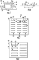
- Figure 1 is a side view of a portion of an example SEIRA stage 20 for use in an SEIRA sensing system.
- Stage 20 serves as a surface for supporting an analyte and for enhancing interactions between impinging infrared light and the analyte for enhanced sensor sensitivity.
- Stage 20 utilizes an architecture that may be reliably and cost-effectively fabricated.
- Stage 20 offers small sized gaps for strong energy localization for enhanced performance.
- Stage 20 comprises substrate 24, island 28 and nano finger 32.
- Substrate 24 comprises a base, foundation or floor for supporting island 28 and nano finger 32.
- substrate 24 comprises a layer of silicon, quartz, ceramic, glass or a polymeric film such as polyethylene teraphalate (PET).
- PET polyethylene teraphalate
- substrate 24 may additionally comprise and interlayer the dielectric material between the silicon substrate and island 28 as well as nano finger 32.
- Such an interlayer dielectric may form from a material such as SiO 2 TEOS, a passivation layer of SiC, silicon nitride, etc.
- other interlayer dielectric materials may be utilized.
- substrate 24 may be formed from other materials.
- Island 28 comprises an upstanding structure and projecting from substrate 24 that has a dimension D parallel to substrate 24 of at least one micrometer. Due to its dimensions of at least one micrometer, island 28 may serve as an antenna that operates at infrared wavelengths. Island 28 is substantially static or non-movable relative to nano finger 32.
- island 28 comprises a base pillar 34 and a plasmonically active island cap 36.
- Base pillar 34 serves as a stem, supporting cap 36.
- a base pillar 34 is formed from a polymer.
- polymer materials from which each pillar 34 may be formed include, but are not limited to, photo resist, PDMS, or a material selected from the group, which includes both dielectric and non-dielectric materials, consisting of a highly cross-linked uv-curable or thermal-curable polymer, a highly cross-linked uv-curable or thermal-curable plastic, a polysiloxane compound, silicon, silicon dioxide, spin-on glass, a solgel material, silicon nitride, diamond, diamond-like carbon, aluminum oxide, sapphire, zinc oxide, and titanium dioxide.
- Cap 36 comprises a plasmonically active or electrically conductive structure formed on top of pillar 34.
- a plasmonically active structure material is a material that converts radiation, such as light or photons, into plasmons, a density wave in an electron gas.
- cap 36 comprises a metal material that enhances the intensity of electromagnetic radiation interacting with the analyte in the gap.
- cap 36 comprises silver, gold, copper, platinum, aluminum, or combinations of these metals in the form of alloys or multilayer systems.
- cap 36 may comprise a material such as indium tin oxide, aluminum zinc oxide, fluorine doped tin oxide, doped zinc oxides, titanium nitride, carbon nanotubes networks and graphene.
- cap 36 may comprise other materials that provide such intensity enhancement.
- Nano finger 32 comprises an elongated nanometer scale flexible columnar support such as a needle, rod, finger or wire that rises up from substrate 24 proximate to island 36.
- nano finger 32 has an aspect ratio of and at least 10:1 (a height of at least 10 times the thickness or diameter).
- such nano finger 32 has a thickness or diameter between 50 nm and 100 nm, while, at the same time, having a height of at least 500 nm and, in one implementation, at least 700 nm.
- nano finger 32 is movable, wherein such columnar structures bend or flex towards island 28 in response to micro-capillary forces or van der Waals forces, wherein such bending facilitates close spacing between the nano finger 32 and island 28 for a smaller gap with enhanced energy localization.
- pillar 44 rises up from substrate 24 at a location sufficiently close to island 28 such that pillar 44 is bendable or closable to a position in which the tip of nano finger 32 is within 1 nm of island 36.
- nano finger 32 comprises a pillar 44 supporting a plasmonically active tip or cap 46.
- pillar 44 comprises an elongate column formed from a polymer material. Pillar 44 serves as a stem supporting cap 46.
- the polymer material facilitates the use of molding, imprinting or other fabrication techniques to form pillar 44.
- the polymer material further facilitates bending and flexing of pillar 44 and subsequently closing during use of stage 20.
- pillar 44 has a diameter of less than a micron. In one implementation of pillar 44 has a diameter of less than or equal to 500 nm.
- polymer materials from which each pillar 44 may be formed include, but are not limited to, photo resist, PDMS, or a flexible material selected from the group, which includes both dielectric and non-dielectric materials, consisting of a highly cross-linked uv-curable or thermal-curable polymer, a highly cross-linked uv-curable or thermal-curable plastic, a polysiloxane compound, silicon, silicon dioxide, spin-on glass, a solgel material, silicon nitride, diamond, diamond-like carbon, aluminum oxide, sapphire, zinc oxide, and titanium dioxide.
- Cap 46 is similar to cap 36 of island 28.
- Cap 46 comprises a plasmonically active or electrically conductive structure formed on top of pillar 44.
- a plasmonically active structure material is a material that converts radiation, such as light or photons, into plasmons, a density wave in an electron gas.
- cap 46 comprises a metal material that enhances the intensity of electromagnetic radiation interacting with the analyte in the gap.
- cap 46 comprises silver, gold, copper, platinum, aluminum, or combinations of these metals in the form of alloys or multilayer systems.
- 36 may comprise a material such as indium tin oxide, aluminum zinc oxide, fluorine doped tin oxide, doped zinc oxides, titanium nitride, carbon nanotubes networks and graphene.
- nano finger cap 46 may comprise other materials that provide such intensity enhancement.
- pillar 44 rises up from substrate 24 at a location sufficiently close to island 28 such that pillar 44 is bendable or closable to a position in which the nano finger cap 46 less than or equal to 5 nm of island cap 36. In some implementations, pillar 44 is bendable or closable to a position in which the nano finger cap 46 is spaced less than or equal to 2 nm from island cap 36.
- FIG. 2 is a flow diagram of an example method 100 that may be used to form a SEIRA stage having small gaps for strong energy localization and enhanced performance.
- method 100 is described with respect to forming a SEIRA state such as stage 20, method 100 may be utilized to form any of the SEIRA stages disclosed herein or similar SEIRA stages.
- static islands extending from a substrate are formed.
- the static islands each have a dimension D parallel to the substrate of at least one micrometer.
- Each static island has a plasmonically active or electrically conductive island cap 36.
- each static island 28 has an elongated cross sectional shape such as an elongated oval or a rectangle, the major dimension or length of the elongated oval or rectangle being at least one micrometer.
- each static island 28 is triangular, having a length or height of at least one micrometer.
- the static island 28 is circular, having a diameter of at least one micrometer.
- the static island 28 may have other cross-sectional shapes having a dimension of at least one micrometer.
- movable nano fingers are formed on the substrate in alignment with the dimension of an adjacent static island.
- the phrase "in alignment with the dimension of an adjacent static island” means that an imaginary line extending along the dimension of the island that is at least one micrometer intersects the nano finger.
- Each of the formed nano fingers has a plasmonically active finger cap that is closable to lessen or equal to 5 nm of the island cap 36 of the adjacent static island 28.
- each of the formed nano fingers has a plasmonically active finger cap that is closable to less than or equal to 2 nm of the island cap 36 of the adjacent static island 28.
- the nano fingers are formed from a material and dimensioned so as to be bendable or flexible such that the cap of the nano finger may move towards the island to provide a gap of less than or equal to 5 nm or less than or equal to 2 nm between the tips or caps of the islands 28 and the nano fingers 32.
- islands 28 and nano fingers 32 are formed on substrate 24 using nano imprint lithography.
- a layer of moldable material, such as a UV resist on substrate 24 is imprinted or embossed with an imprint master, such as a quartz master, wherein ultraviolet light is applied to solidify or cure the patterned UV resist. Sacrifice or withdraw of the imprint master leaves the remaining substrate and formed pillars 34, 44 up standing from the substrate 24. The pillars are then topped with the caps 36, 46.
- FIG. 3 is a schematic diagram of a portion of an example SEIRA sensing system 200 comprising stage 20.
- sensing system 200 comprises infrared emitter 202 and infrared sensor 204.
- Emitter 202 and sensor 204 interrogate analyte molecules at a frequency resonant to those of molecular vibrations.
- Emitter 202 comprises a device that emits and directs infrared (wavelength 3-30 microns) or near infrared (wavelength 0.7-3 microns) radiation towards stage 20, towards island 28 and nano finger 32.
- Infrared sources may include, but are not limited to, thermal sources such as Globar filaments, infrared LEDs and infrared lasers sources.
- Infrared sensor 204 comprise a device that senses the infrared radiation absorbed by the analyte molecules such as by sensing the quantity of the emitted infrared radiation that is transmitted or reflected back towards sensor 204.
- Infrared sensors may include Mercurium-Cadmium-Telluride sensors, microbolometers, Indium gallium arsenide, indium antimonide and imaging arrays of such sensing elements.
- the amount of energy absorbed by a molecule may serve as a fingerprint facilitating identification of the analyte molecules or to identify characteristics of the analyte molecules.
- Figure 4 is a flow diagram of an example method 300 for analyzing an analyte using SEIRA. Method 300 is described as carried out using system 200 and is illustrated in Figure 3 . It should be appreciated that method 300 may be carried out using other SEIRA sensing systems or other SEIRA stages similar to stage 20.
- an analyte 50 is applied to an SEIRA stage, such as stage 20.
- the stage comprises a substrate 24, a static island 28 and a movable nano finger 32.
- the static island 28 extends from the substrate 24 and has a dimension D parallel to the substrate of at least one micrometer and a plasmonicaly active/electrically conductive island cap 36.
- the movable nano finger 32 extends from the substrate and is aligned with the dimension D.
- the movable nano finger 32 has a plasmonicaly active or electrically conductive finger cap 46 and is closable to less than or equal to 5 nm of the island cap 36. In one implementation, cap 46 is bendable or closable to less than or equal to 2 nm of the island cap 36.
- the finger cap 46 is closed with respect to or towards the island cap 36.
- the analyte 50 is applied as part of a liquid, wherein liquid is evaporated, leaving the analyte deposited upon island cap 36 and finger cap 46, captured between or within the gap separating island cap 36 and finger cap 46.
- the evaporation of the liquid creates capillary forces sufficient to draw and bend nano finger 32 towards island 28.
- the evaporation of the liquid is accelerated through the application of heat to stage 20.
- the closing of the island cap 36 and the finger cap 46 may be facilitated in other fashions.
- nano finger 32 may be heated to a temperature approaching or above its glass transition temperature, causing nano finger 32 to collapse and bend towards island 28.
- the larger size and mass of island 28 may slow the rate at which the temperature of island 28 rises such that nano finger 32 collapses towards island 28.
- IR emitter 202 irradiates stage 20, impinging the analyte 50, island cap 36 and finger cap 46 with infrared or near infrared radiation 54.
- sensor 204 senses infrared radiation absorption by the molecules 50. In one implementation, sensor 204 determines the amount of infrared radiation that has been absorbed based upon the quantity of infrared radiation directed at stage 20 and by sensing the quantity of infrared radiation not absorbed, transmitted or reflected back towards sensor 204.
- the quantity of infrared radiation absorbed by analyte 50 may be utilized to analyze the analyte 50, indicating an identity of the analyte 50 or indicating characteristics of the analyte 50.
- FIGS 5 and 6 illustrate SEIRA stage 420, an example implementation of SEIRA stage 20.
- SEIRA stage 420 may be utilized as part of sensing system 200 in place of stage 20.
- Stage 420 is similar to stage 20 described above except that stage 420 is specifically illustrated as comprising a static island 428 in view of island 28. Those remaining components of stage 420 which correspond to components of stage 20 are numbered similarly.
- Static island 428 is similar to island 28 except that static island 428 is specifically illustrated as having an elongate rectangular or rod cross sectional shape having a major dimension D of at least 1 ⁇ m. Similar to island 28, static island 428 comprise a stem or base pillar 34 and a static island cap 36. The major dimension C of static island 428 is aligned with nano finger 28. In other words, an imaginary linear line 451 extending along dimension D, through or upon the top of cap 36, intersects cap 46 of nano finger 32.
- static island 428 serves as an antenna that operates at infrared wavelengths.
- nano finger 32 has an elongated aspect ratio facilitating bending of nano finger 32 towards island 36, namely towards the end of the elongated rectangle, so as to close caps 36 and 46 to less than or equal to 5 nm, and in one implementation less than or equal to 2 nm, of one another.
- This single-digit nanometer scale gap G after closure or bending, provides a hotspot of high optical energy concentration which results in strong spectroscopic signal response.
- FIG. 7 is a top view of an example SEIRA stage 520 fabricated using nano imprint lithography.
- stage 520 may be formed using other techniques.
- Stage 520 comprises a grid or array of island-nano finger pairs 522, each pair 522 comprising a static island 428 and an associated nano finger 32 as described above.
- Each pair 522 provides a self-limited single-digit nanometer sized gap, upon closure of the caps 36, 46, to provide multiple hotspots of high optical energy concentration which result in strong spectroscopic signal response.
- FIG 8 is a top view of a portion of another example SEIRA stage 620 that may be fabricated using nano imprint lithography. In other implementations, stage 620 may be formed using other techniques. Stage 620 may be utilized as part of SEIRA sensing system 200 described above in place of stage 20. Stage 620 is similar to stage 520 described above except that stage 620 comprises a grid or array of island-nano finger pairs 622 in place of pairs 522. Pairs 622 are similar to pairs 522 except that each pair 622 additionally comprises a second movable nano finger 634 on an opposite and of island 428 as nano finger 34. Nano finger 634 is similar to nano finger 34 in that nano finger 34 comprises a pillar 44 (shown in Figure 5 ) that supports a cap 46. As with nano finger 34, the major dimension D of static island 428 is aligned with nano finger 634.
- nano finger 634 is bendable or closable with respect to island 428.
- the cap 46 of nano finger 634 is closable to within 1 nm of cap 36 of island 428.
- pairs 622 of stage 620 each provide two self-limited single-digit nanometer sized gaps, upon closure of the caps 36, 46, to provide multiple hotspots of high optical energy concentration which result in strong spectroscopic signal response.
- Figure 9 is a top view of a portion of another example SEIRA stage 720 that may be fabricated using nano imprint lithography.
- stage 720 may be formed using other techniques.
- Stage 720 is similar to stage 520 described above except that stage 720 comprises a grid or array of island-nano finger pairs 722 in place of pairs 522. Pairs 722 are similar to pairs 522 except that each of pairs 722 comprises a triangular shaped island 728 paired with a movable nano finger 32 (described above).
- Island 728 each have an underlying base pillar that supports a plasmonically active cap 736. As shown by Figure 9 , the underlying base pillar and the cap 736 each have a triangular cross sectional shape.
- the underlying base pillar has a size and shape corresponding to the size and shape of the cap 736 seen in the top view shown in Figure 9 .
- Each of the triangular islands has a height dimension H (the dimension from the base to the apex of the triangle opposite nano finger 32) of at least one micrometer.
- the triangular shape of island 728 serves as an infrared antenna which is more broadband, facilitating use of a wider range of wavelengths of radiation in the infrared spectrum when performing SEIRA analysis.
- each pair 722 provides a self-limited single-digit nanometer sized gap, upon closure of the caps 736, 46, to provide a hotspot of high optical energy concentration which results in a strong spectroscopic signal response.
- each of the pairs 722 are illustrated as having the same orientation, in other implementations, such pairs 722 may have opposite orientations or may have a variety of different orientations on substrate 24.
- FIG 10 is a top view of a portion of another example SEIRA stage 820 that may be fabricated using nano imprint lithography.
- stage 820 may be formed using other techniques.
- Stage 820 is similar to stage 520 described above except that stage 820 comprises a grid or array of island-nano finger clusters 822 in place of pairs 522.
- Clusters 822 each comprise a static cylindrical center island 828 surrounded by or encircled by multiple spaced movable nano fingers 32 (described above).
- Each of islands 828 has a cylindrical underlying base pillar that supports a plasmonically active cap 836. As shown by Figure 10 , the underlying base pillar and the cap 736 each have a circular cross sectional shape. The underlying base pillar has a size and shape corresponding to the size and shape of the cap 836 seen in the top view shown in Figure 10 . Each of the cylindrical islands has a cap 836 with a diameter at least one micrometer.
- nano fingers 32 bend or flex inwardly towards the center of their associated center island 828.
- caps 46 of nano fingers 32 close to within 1 nm of the cap 836 of island 828.
- Each cluster 822 provides a multitude of self-limited single-digit nanometer sized gaps corresponding to the number of nano fingers 32 surrounding island 828, upon closure of the caps 836, 46, to provide a multitude of hotspots of high optical energy concentration which results in a strong spectroscopic signal response.
- clusters 822 are illustrated as comprising a same number of nano fingers 32 and as specifically comprising 12 nano fingers 32 about each island 828, in other implementations, clusters 822 may have a different total number of nano fingers 32 about each island 828. Moreover, in some implementations, different clusters may have different numbers of nano fingers 832 about the respective islands 828.
- each cluster 822 further provides polarization insensitivity.
- clusters 822 may provide high degrees of SEIRA sensitivity when unpolarized infrared or near-infrared light is being used to illuminate, interrogate or irradiate the analyte captured and retained on each cluster 822.
- the center island may have an oval cross-section instead of circular to allow controlled polarization-selective antenna responses.
- FIG 11 is a diagram schematically illustrating another example sensing system 900.
- Sensing system 900 offers greater versatility in that sensing system 900 facilitates both surface enehanced SEIRA analysis and surface enhanced Raman spectroscopy analysis of an analyte.
- system 900 may apply both types of analysis to a same analyte on a same stage.
- Sensing system 900 comprises stage 620, infrared emitter/detector 902, Raman emitter/detector 906, input 908 and controller 910.
- Stage 620 is described above. It should be appreciated that system 900 may be utilized with any of the stages described above as well as other similar stages having a static island have a plasmonically active cap with a dimension parallel to the substrate of at least one micrometer and a movable nano finger aligned with the dimensions of the cap, wherein the nano finger has a plasmonically active cap closable to a spacing of less than or equal to 5 nm from the island cap.
- Infrared emitter/detector 902 comprises IR emitter 202 and sensor 204 described above with respect to system 200. Infrared emitter/detector 902 interrogates analyte molecules at a frequency at which there are molecular vibrations without shifting the frequency of such molecules. Infrared emitter/detector 902 comprises a device that emits and directs infrared or near infrared radiation towards stage 620, towards island 428 and nano fingers 32, 632.
- Infrared emitter/detector 902 further comprises a device that senses the infrared radiation absorbed by the analyte molecules such as by sensing the quantity of infrared radiation that is reflected back or transmitted towards the infrared emitter/detector 902.
- the amount of energy absorbed by a molecule may serve as a fingerprint facilitating identification of the analyte molecules or to identify characteristics of the analyte molecules.
- Raman emitter/detector 906 comprises a device that directs light, such as a laser beam of light, towards and onto stage 620 and a device that focuses, gathers and detects and SERS spectra resulting from light scattering by the sample analyte on island 428 and nano fingers 32, 632.
- emitter/detector 906 comprises an infrared laser to emit a beam having a wavelength of 785 nm onto island 428 and nano fingers 32, 632.
- Raman emitter/detector 906 may include one or more optical components such as lenses and mirrors.
- the received SERS spectra, including shifts in the frequency of light, is compared against previous identified spectrum fingerprints or signatures to identify characteristics of the sample analyte.
- Input 908 comprise a device by which selections or commands may be provided to controller 910 indicating whether system 900 is to operate in either an SEIRA detection mode or a Raman spectroscopy detection mode.
- Input 908 may comprise a touch screen, a mouse, a keyboard, a touchpad, a microphone with speech recognition and the like.
- input 908 may comprise a pushbutton, toggle switch or other manual input device.
- Controller 910 comprises electronic hardware, such as a processing unit, to carry out instructions contained in a non-transitory computer-readable medium or memory. Controller 910 selectively activates emitter/detector 902 or emitter/detector 906 in response to instructions received via the input 908. Because stage 620 (or any of the other stages described above, comprises at least one nano finger 32 that is bendable or closable towards and associated island 20, 428, 728, 828, stage 620 is well-suited for serving as an analyte supporting surface that facilitate surface enhanced Raman spectroscopy.
- system 900 may be used to first identify one or more characteristics of an analyte using SEIRA and then to either confirm the results or to identify additional characteristics of the analyte using surface enhanced Raman spectroscopy (SERS).
- SEIRA surface enhanced Raman spectroscopy
Landscapes
- Chemical & Material Sciences (AREA)
- Health & Medical Sciences (AREA)
- Biochemistry (AREA)
- Life Sciences & Earth Sciences (AREA)
- Physics & Mathematics (AREA)
- Analytical Chemistry (AREA)
- General Health & Medical Sciences (AREA)
- General Physics & Mathematics (AREA)
- Immunology (AREA)
- Pathology (AREA)
- Nuclear Medicine, Radiotherapy & Molecular Imaging (AREA)
- Engineering & Computer Science (AREA)
- Nanotechnology (AREA)
- Investigating, Analyzing Materials By Fluorescence Or Luminescence (AREA)
- Investigating Or Analysing Materials By Optical Means (AREA)
Description
- Surface enhanced infrared absorption (SEIRA) is sometimes used for analyzing the structure of an analyte such as inorganic materials and complex organic molecules. SEIRA focuses infrared radiation or light onto the analyte, wherein the interaction between the light and the analyte is detected for analysis.
-
US2013/070241 A1 relates to an asymmetrical-nanofinger device for surface-enhanced luminescence. The device includes a substrate, and a plurality of nanofingers coupled with the substrate. The plurality of nanofingers includes a primary nanofinger having a primary active-material cap, and a secondary nanofinger having a secondary active-material cap. An average diameter of the primary active-material cap is substantially greater than an average diameter of the secondary active-material cap. -
-
Figure 1 is a side view schematically illustrating a portion of an example SEIRA stage. -
Figure 2 is a flow diagram of an example method for forming an example SEIRA stage. -
Figure 3 is a side view schematically illustrating a portion of an example SEIRA sensing system. -
Figure 4 is a flow diagram of an example method for analyzing and analyte using an example SEIRA sensing system. -
Figure 5 is a perspective view of a portion of another example SEIRA stage. -
Figure 6 is a top view of the example SEIRA stage ofFigure 5 . -
Figure 7 is a top view of a portion of another example SEIRA stage. -
Figure 8 is a top view of a portion of another example SEIRA stage. -
Figure 9 is a top view of a portion of another example SEIRA stage. -
Figure 10 is a top view of a portion of another example SEIRA stage. -
Figure 11 is a side view schematically illustrating a portion of an example SEIRA /surface enhanced Raman spectroscopy (SERS) sensing system. - Throughout the drawings, identical reference numbers designate similar, but not necessarily identical, elements. The figures are not necessarily to scale, and the size of some parts may be exaggerated to more clearly illustrate the example shown. Moreover the drawings provide examples and/or implementations consistent with the description; however, the description is not limited to the examples and/or implementations provided in the drawings.
- SEIRA utilizes energy localization gaps between neighboring electrically conductive or metallic surfaces. Reducing the size of the gaps may enhance performance. Disclosed herein are examples of SEIRA stages that offer small, controlled self-limited single digit nanometer gaps for strong energy localization/strong signal strength while at the same time being more economical to fabricate.
- The example SEIRA stages comprise flexible nano fingers and wider protruding islands. The islands exhibit a footprint that facilitates operation at infrared wavelengths. The nano fingers are flexible so as to lean towards the islands to create self-limiting nano gaps of less than or equal to 5 nm and as little as 1 to 2 nm, creating hot spots of high optical energy concentration resulting in strong spectroscopic signal response. Because the nano gaps are formed by closure of the nano fingers and the islands, the size of the nano gaps therebetween is not wholly dependent on fabrication density or resolution, facilitating lower cost fabrication techniques.
- Disclosed herein is an example SEIRA stage that may comprise a substrate, a static island extending from the substrate and a movable nano finger extending from the substrate. The static island may have a plasmonically active island cap and a dimension parallel to the substrate of at least one micrometer. The movable nano finger may be aligned with the dimension. The movable nano finger may have a plasmonicaly active finger cap closable to less than or equal to 5 nm of the island cap.
- Disclosed herein is an example method for analyzing and analyte using SEIRA. The method may comprise applying an analyte to a SEIRA stage. SEIRA stage may comprise a substrate, a static island extending from the substrate and a movable nano finger extending from the substrate. The static island may have a plasmonically active island cap and a dimension parallel to the substrate of at least one micrometer. The movable nano finger may be aligned with the dimension. The movable nano finger may have a plasmonicaly active finger cap closable to less than or equal to 5 nm of the island cap. The method may further include closing the finger cap towards the island cap, irradiating the finger cap and the island cap and sensing infrared absorption to analyze the analyte.
- Disclosed herein is an example method for forming a SEIRA stage. The method may comprise forming static islands extending from a substrate, each of the static islands having a dimension parallel to the substrate of at least one micrometer, wherein each static island has a plasmonically active island cap. The method may further comprise forming movable nano fingers extending from the substrate, wherein each of the nano fingers is aligned with the dimension of an adjacent static island. Each movable nano finger may have a plasmonicaly active finger cap closable to less than or equal to 5 nm of the island cap the adjacent static island.
-
Figure 1 is a side view of a portion of anexample SEIRA stage 20 for use in an SEIRA sensing system.Stage 20 serves as a surface for supporting an analyte and for enhancing interactions between impinging infrared light and the analyte for enhanced sensor sensitivity.Stage 20 utilizes an architecture that may be reliably and cost-effectively fabricated.Stage 20 offers small sized gaps for strong energy localization for enhanced performance.Stage 20 comprisessubstrate 24,island 28 andnano finger 32. -
Substrate 24 comprises a base, foundation or floor for supportingisland 28 andnano finger 32. In one implementation,substrate 24 comprises a layer of silicon, quartz, ceramic, glass or a polymeric film such as polyethylene teraphalate (PET). In some implementations,substrate 24 may additionally comprise and interlayer the dielectric material between the silicon substrate andisland 28 as well asnano finger 32. Such an interlayer dielectric may form from a material such as SiO2 TEOS, a passivation layer of SiC, silicon nitride, etc. In other implementations, other interlayer dielectric materials may be utilized. In still other implementations,substrate 24 may be formed from other materials. - Island 28 comprises an upstanding structure and projecting from
substrate 24 that has a dimension D parallel tosubstrate 24 of at least one micrometer. Due to its dimensions of at least one micrometer,island 28 may serve as an antenna that operates at infrared wavelengths. Island 28 is substantially static or non-movable relative tonano finger 32. - In the example illustrated,
island 28 comprises abase pillar 34 and a plasmonicallyactive island cap 36.Base pillar 34 serves as a stem, supportingcap 36. In one implementation abase pillar 34 is formed from a polymer. Examples of polymer materials from which eachpillar 34 may be formed include, but are not limited to, photo resist, PDMS, or a material selected from the group, which includes both dielectric and non-dielectric materials, consisting of a highly cross-linked uv-curable or thermal-curable polymer, a highly cross-linked uv-curable or thermal-curable plastic, a polysiloxane compound, silicon, silicon dioxide, spin-on glass, a solgel material, silicon nitride, diamond, diamond-like carbon, aluminum oxide, sapphire, zinc oxide, and titanium dioxide. -
Cap 36 comprises a plasmonically active or electrically conductive structure formed on top ofpillar 34. A plasmonically active structure material is a material that converts radiation, such as light or photons, into plasmons, a density wave in an electron gas. In one implementation,cap 36 comprises a metal material that enhances the intensity of electromagnetic radiation interacting with the analyte in the gap. In one implementation,cap 36 comprises silver, gold, copper, platinum, aluminum, or combinations of these metals in the form of alloys or multilayer systems. In one implementation,cap 36 may comprise a material such as indium tin oxide, aluminum zinc oxide, fluorine doped tin oxide, doped zinc oxides, titanium nitride, carbon nanotubes networks and graphene. In another implementation,cap 36 may comprise other materials that provide such intensity enhancement. -
Nano finger 32 comprises an elongated nanometer scale flexible columnar support such as a needle, rod, finger or wire that rises up fromsubstrate 24 proximate toisland 36. In one implementation,nano finger 32 has an aspect ratio of and at least 10:1 (a height of at least 10 times the thickness or diameter). In one implementation,such nano finger 32 has a thickness or diameter between 50 nm and 100 nm, while, at the same time, having a height of at least 500 nm and, in one implementation, at least 700 nm. In the example illustrated,nano finger 32 is movable, wherein such columnar structures bend or flex towardsisland 28 in response to micro-capillary forces or van der Waals forces, wherein such bending facilitates close spacing between thenano finger 32 andisland 28 for a smaller gap with enhanced energy localization. In one implementation,pillar 44 rises up fromsubstrate 24 at a location sufficiently close toisland 28 such thatpillar 44 is bendable or closable to a position in which the tip ofnano finger 32 is within 1 nm ofisland 36. - As schematically shown by
Figure 1 ,nano finger 32 comprises apillar 44 supporting a plasmonically active tip orcap 46. In one implementation,pillar 44 comprises an elongate column formed from a polymer material.Pillar 44 serves as astem supporting cap 46. The polymer material facilitates the use of molding, imprinting or other fabrication techniques to formpillar 44. The polymer material further facilitates bending and flexing ofpillar 44 and subsequently closing during use ofstage 20. In one implementation,pillar 44 has a diameter of less than a micron. In one implementation ofpillar 44 has a diameter of less than or equal to 500 nm. Examples of polymer materials from which eachpillar 44 may be formed include, but are not limited to, photo resist, PDMS, or a flexible material selected from the group, which includes both dielectric and non-dielectric materials, consisting of a highly cross-linked uv-curable or thermal-curable polymer, a highly cross-linked uv-curable or thermal-curable plastic, a polysiloxane compound, silicon, silicon dioxide, spin-on glass, a solgel material, silicon nitride, diamond, diamond-like carbon, aluminum oxide, sapphire, zinc oxide, and titanium dioxide. -
Cap 46 is similar to cap 36 ofisland 28.Cap 46 comprises a plasmonically active or electrically conductive structure formed on top ofpillar 44. A plasmonically active structure material is a material that converts radiation, such as light or photons, into plasmons, a density wave in an electron gas. In one implementation,cap 46 comprises a metal material that enhances the intensity of electromagnetic radiation interacting with the analyte in the gap. In one implementation,cap 46 comprises silver, gold, copper, platinum, aluminum, or combinations of these metals in the form of alloys or multilayer systems. In one implementation, 36 may comprise a material such as indium tin oxide, aluminum zinc oxide, fluorine doped tin oxide, doped zinc oxides, titanium nitride, carbon nanotubes networks and graphene. In another implementation,nano finger cap 46 may comprise other materials that provide such intensity enhancement. In the example illustrated,pillar 44 rises up fromsubstrate 24 at a location sufficiently close toisland 28 such thatpillar 44 is bendable or closable to a position in which thenano finger cap 46 less than or equal to 5 nm ofisland cap 36. In some implementations,pillar 44 is bendable or closable to a position in which thenano finger cap 46 is spaced less than or equal to 2 nm fromisland cap 36. -
Figure 2 is a flow diagram of anexample method 100 that may be used to form a SEIRA stage having small gaps for strong energy localization and enhanced performance. Althoughmethod 100 is described with respect to forming a SEIRA state such asstage 20,method 100 may be utilized to form any of the SEIRA stages disclosed herein or similar SEIRA stages. As indicated byblock 110, static islands extending from a substrate are formed. The static islands each have a dimension D parallel to the substrate of at least one micrometer. Each static island has a plasmonically active or electricallyconductive island cap 36. - In one implementation, each
static island 28 has an elongated cross sectional shape such as an elongated oval or a rectangle, the major dimension or length of the elongated oval or rectangle being at least one micrometer. In one implementation, eachstatic island 28 is triangular, having a length or height of at least one micrometer. In yet another implementation, thestatic island 28 is circular, having a diameter of at least one micrometer. In yet other implementations, thestatic island 28 may have other cross-sectional shapes having a dimension of at least one micrometer. - As indicated by
block 114, movable nano fingers are formed on the substrate in alignment with the dimension of an adjacent static island. The phrase "in alignment with the dimension of an adjacent static island" means that an imaginary line extending along the dimension of the island that is at least one micrometer intersects the nano finger. Each of the formed nano fingers has a plasmonically active finger cap that is closable to lessen or equal to 5 nm of theisland cap 36 of the adjacentstatic island 28. In one implementation, each of the formed nano fingers has a plasmonically active finger cap that is closable to less than or equal to 2 nm of theisland cap 36 of the adjacentstatic island 28. In other words, the nano fingers are formed from a material and dimensioned so as to be bendable or flexible such that the cap of the nano finger may move towards the island to provide a gap of less than or equal to 5 nm or less than or equal to 2 nm between the tips or caps of theislands 28 and thenano fingers 32. - In one implementation,
islands 28 andnano fingers 32 are formed onsubstrate 24 using nano imprint lithography. With nano imprint lithography, a layer of moldable material, such as a UV resist, onsubstrate 24 is imprinted or embossed with an imprint master, such as a quartz master, wherein ultraviolet light is applied to solidify or cure the patterned UV resist. Sacrifice or withdraw of the imprint master leaves the remaining substrate and formedpillars substrate 24. The pillars are then topped with thecaps -
Figure 3 is a schematic diagram of a portion of an exampleSEIRA sensing system 200 comprisingstage 20. In addition tostage 20,sensing system 200 comprisesinfrared emitter 202 andinfrared sensor 204.Emitter 202 andsensor 204 interrogate analyte molecules at a frequency resonant to those of molecular vibrations.Emitter 202 comprises a device that emits and directs infrared (wavelength 3-30 microns) or near infrared (wavelength 0.7-3 microns) radiation towardsstage 20, towardsisland 28 andnano finger 32. Infrared sources may include, but are not limited to, thermal sources such as Globar filaments, infrared LEDs and infrared lasers sources.Infrared sensor 204 comprise a device that senses the infrared radiation absorbed by the analyte molecules such as by sensing the quantity of the emitted infrared radiation that is transmitted or reflected back towardssensor 204. Infrared sensors may include Mercurium-Cadmium-Telluride sensors, microbolometers, Indium gallium arsenide, indium antimonide and imaging arrays of such sensing elements. The amount of energy absorbed by a molecule may serve as a fingerprint facilitating identification of the analyte molecules or to identify characteristics of the analyte molecules. -
Figure 4 is a flow diagram of anexample method 300 for analyzing an analyte using SEIRA.Method 300 is described as carried out usingsystem 200 and is illustrated inFigure 3 . It should be appreciated thatmethod 300 may be carried out using other SEIRA sensing systems or other SEIRA stages similar tostage 20. - As indicated by
block 310 and illustrated inFigure 3 , ananalyte 50 is applied to an SEIRA stage, such asstage 20. As described above, the stage comprises asubstrate 24, astatic island 28 and amovable nano finger 32. Thestatic island 28 extends from thesubstrate 24 and has a dimension D parallel to the substrate of at least one micrometer and a plasmonicaly active/electricallyconductive island cap 36. Themovable nano finger 32 extends from the substrate and is aligned with the dimension D. Themovable nano finger 32 has a plasmonicaly active or electricallyconductive finger cap 46 and is closable to less than or equal to 5 nm of theisland cap 36. In one implementation,cap 46 is bendable or closable to less than or equal to 2 nm of theisland cap 36. - As indicated by
block 314 and further shown inFigure 3 , thefinger cap 46 is closed with respect to or towards theisland cap 36. In one implementation, theanalyte 50 is applied as part of a liquid, wherein liquid is evaporated, leaving the analyte deposited uponisland cap 36 andfinger cap 46, captured between or within the gap separatingisland cap 36 andfinger cap 46. The evaporation of the liquid creates capillary forces sufficient to draw and bendnano finger 32 towardsisland 28. In one implementation, the evaporation of the liquid is accelerated through the application of heat to stage 20. - In other implementations, the closing of the
island cap 36 and thefinger cap 46 may be facilitated in other fashions. For example, in other implementations,nano finger 32 may be heated to a temperature approaching or above its glass transition temperature, causingnano finger 32 to collapse and bend towardsisland 28. The larger size and mass ofisland 28 may slow the rate at which the temperature ofisland 28 rises such thatnano finger 32 collapses towardsisland 28. - As indicated by
block 318 and illustrated inFigure 3 ,IR emitter 202 irradiatesstage 20, impinging theanalyte 50,island cap 36 andfinger cap 46 with infrared or nearinfrared radiation 54. As indicated byblock 320,sensor 204 senses infrared radiation absorption by themolecules 50. In one implementation,sensor 204 determines the amount of infrared radiation that has been absorbed based upon the quantity of infrared radiation directed atstage 20 and by sensing the quantity of infrared radiation not absorbed, transmitted or reflected back towardssensor 204. The quantity of infrared radiation absorbed by analyte 50 (or not absorbed by analyte 50) may be utilized to analyze theanalyte 50, indicating an identity of theanalyte 50 or indicating characteristics of theanalyte 50. -
Figures 5 and 6 illustrateSEIRA stage 420, an example implementation ofSEIRA stage 20.SEIRA stage 420 may be utilized as part ofsensing system 200 in place ofstage 20.Stage 420 is similar to stage 20 described above except thatstage 420 is specifically illustrated as comprising astatic island 428 in view ofisland 28. Those remaining components ofstage 420 which correspond to components ofstage 20 are numbered similarly. -
Static island 428 is similar toisland 28 except thatstatic island 428 is specifically illustrated as having an elongate rectangular or rod cross sectional shape having a major dimension D of at least 1 µm. Similar toisland 28,static island 428 comprise a stem orbase pillar 34 and astatic island cap 36. The major dimension C ofstatic island 428 is aligned withnano finger 28. In other words, an imaginarylinear line 451 extending along dimension D, through or upon the top ofcap 36, intersectscap 46 ofnano finger 32. - As with
static island 28, because the dimension D that is aligned withnano finger 28 is at least 1 µm,static island 428 serves as an antenna that operates at infrared wavelengths. As withstage 20,nano finger 32 has an elongated aspect ratio facilitating bending ofnano finger 32 towardsisland 36, namely towards the end of the elongated rectangle, so as to closecaps -
Figure 7 is a top view of anexample SEIRA stage 520 fabricated using nano imprint lithography. In other implementations,stage 520 may be formed using other techniques.Stage 520 comprises a grid or array of island-nano finger pairs 522, eachpair 522 comprising astatic island 428 and an associatednano finger 32 as described above. Eachpair 522 provides a self-limited single-digit nanometer sized gap, upon closure of thecaps -
Figure 8 is a top view of a portion of anotherexample SEIRA stage 620 that may be fabricated using nano imprint lithography. In other implementations,stage 620 may be formed using other techniques.Stage 620 may be utilized as part ofSEIRA sensing system 200 described above in place ofstage 20.Stage 620 is similar to stage 520 described above except thatstage 620 comprises a grid or array of island-nano finger pairs 622 in place ofpairs 522.Pairs 622 are similar topairs 522 except that eachpair 622 additionally comprises a secondmovable nano finger 634 on an opposite and ofisland 428 asnano finger 34.Nano finger 634 is similar tonano finger 34 in thatnano finger 34 comprises a pillar 44 (shown inFigure 5 ) that supports acap 46. As withnano finger 34, the major dimension D ofstatic island 428 is aligned withnano finger 634. - Like
nano finger 34,nano finger 634 is bendable or closable with respect toisland 428. Thecap 46 ofnano finger 634 is closable to within 1 nm ofcap 36 ofisland 428. Unlikepairs 522, pairs 622 ofstage 620 each provide two self-limited single-digit nanometer sized gaps, upon closure of thecaps -
Figure 9 is a top view of a portion of another example SEIRA stage 720 that may be fabricated using nano imprint lithography. In other implementations, stage 720 may be formed using other techniques. Stage 720 is similar to stage 520 described above except that stage 720 comprises a grid or array of island-nano finger pairs 722 in place ofpairs 522.Pairs 722 are similar topairs 522 except that each ofpairs 722 comprises a triangular shapedisland 728 paired with a movable nano finger 32 (described above). -
Island 728 each have an underlying base pillar that supports a plasmonicallyactive cap 736. As shown byFigure 9 , the underlying base pillar and thecap 736 each have a triangular cross sectional shape. The underlying base pillar has a size and shape corresponding to the size and shape of thecap 736 seen in the top view shown inFigure 9 . Each of the triangular islands has a height dimension H (the dimension from the base to the apex of the triangle opposite nano finger 32) of at least one micrometer. The triangular shape ofisland 728 serves as an infrared antenna which is more broadband, facilitating use of a wider range of wavelengths of radiation in the infrared spectrum when performing SEIRA analysis. - The apex of the triangular shape of each
island 728 points to and extends opposite to the pairedmovable nano finger 32. As in the above described stages, eachpair 722 provides a self-limited single-digit nanometer sized gap, upon closure of thecaps pairs 722 are illustrated as having the same orientation, in other implementations,such pairs 722 may have opposite orientations or may have a variety of different orientations onsubstrate 24. -
Figure 10 is a top view of a portion of anotherexample SEIRA stage 820 that may be fabricated using nano imprint lithography. In other implementations,stage 820 may be formed using other techniques.Stage 820 is similar to stage 520 described above except thatstage 820 comprises a grid or array of island-nano finger clusters 822 in place ofpairs 522.Clusters 822 each comprise a staticcylindrical center island 828 surrounded by or encircled by multiple spaced movable nano fingers 32 (described above). - Each of
islands 828 has a cylindrical underlying base pillar that supports a plasmonicallyactive cap 836. As shown byFigure 10 , the underlying base pillar and thecap 736 each have a circular cross sectional shape. The underlying base pillar has a size and shape corresponding to the size and shape of thecap 836 seen in the top view shown inFigure 10 . Each of the cylindrical islands has acap 836 with a diameter at least one micrometer. - During closure and movement of the
nano fingers 32,nano fingers 32 bend or flex inwardly towards the center of their associatedcenter island 828. During such closure, caps 46 ofnano fingers 32 close to within 1 nm of thecap 836 ofisland 828. Eachcluster 822 provides a multitude of self-limited single-digit nanometer sized gaps corresponding to the number ofnano fingers 32 surroundingisland 828, upon closure of thecaps clusters 822 are illustrated as comprising a same number ofnano fingers 32 and as specifically comprising 12nano fingers 32 about eachisland 828, in other implementations,clusters 822 may have a different total number ofnano fingers 32 about eachisland 828. Moreover, in some implementations, different clusters may have different numbers of nano fingers 832 about therespective islands 828. - In addition to providing a multitude of hotspots equal to the number of
nano fingers 32 about theisland 828, the dot-flower arrangement of eachcluster 822 further provides polarization insensitivity. In other words,clusters 822 may provide high degrees of SEIRA sensitivity when unpolarized infrared or near-infrared light is being used to illuminate, interrogate or irradiate the analyte captured and retained on eachcluster 822. In other instances, the center island may have an oval cross-section instead of circular to allow controlled polarization-selective antenna responses. -
Figure 11 is a diagram schematically illustrating anotherexample sensing system 900.Sensing system 900 offers greater versatility in thatsensing system 900 facilitates both surface enehanced SEIRA analysis and surface enhanced Raman spectroscopy analysis of an analyte. In addition to being able to carry out both Raman spectroscopy and SEIRA analysis,system 900 may apply both types of analysis to a same analyte on a same stage. -
Sensing system 900 comprisesstage 620, infrared emitter/detector 902, Raman emitter/detector 906,input 908 andcontroller 910.Stage 620 is described above. It should be appreciated thatsystem 900 may be utilized with any of the stages described above as well as other similar stages having a static island have a plasmonically active cap with a dimension parallel to the substrate of at least one micrometer and a movable nano finger aligned with the dimensions of the cap, wherein the nano finger has a plasmonically active cap closable to a spacing of less than or equal to 5 nm from the island cap. - Infrared emitter/
detector 902 comprisesIR emitter 202 andsensor 204 described above with respect tosystem 200. Infrared emitter/detector 902 interrogates analyte molecules at a frequency at which there are molecular vibrations without shifting the frequency of such molecules. Infrared emitter/detector 902 comprises a device that emits and directs infrared or near infrared radiation towardsstage 620, towardsisland 428 andnano fingers detector 902 further comprises a device that senses the infrared radiation absorbed by the analyte molecules such as by sensing the quantity of infrared radiation that is reflected back or transmitted towards the infrared emitter/detector 902. The amount of energy absorbed by a molecule may serve as a fingerprint facilitating identification of the analyte molecules or to identify characteristics of the analyte molecules. - Raman emitter/detector 906 comprises a device that directs light, such as a laser beam of light, towards and onto
stage 620 and a device that focuses, gathers and detects and SERS spectra resulting from light scattering by the sample analyte onisland 428 andnano fingers island 428 andnano fingers island 428 andnano fingers - Input 908 comprise a device by which selections or commands may be provided to
controller 910 indicating whethersystem 900 is to operate in either an SEIRA detection mode or a Raman spectroscopy detection mode. Input 908 may comprise a touch screen, a mouse, a keyboard, a touchpad, a microphone with speech recognition and the like. In some implementations,input 908 may comprise a pushbutton, toggle switch or other manual input device. -
Controller 910 comprises electronic hardware, such as a processing unit, to carry out instructions contained in a non-transitory computer-readable medium or memory.Controller 910 selectively activates emitter/detector 902 or emitter/detector 906 in response to instructions received via theinput 908. Because stage 620 (or any of the other stages described above, comprises at least onenano finger 32 that is bendable or closable towards and associatedisland stage 620 is well-suited for serving as an analyte supporting surface that facilitate surface enhanced Raman spectroscopy. As a result, through appropriate input tocontroller 910,system 900 may be used to first identify one or more characteristics of an analyte using SEIRA and then to either confirm the results or to identify additional characteristics of the analyte using surface enhanced Raman spectroscopy (SERS). - Although the present disclosure has been described with reference to example implementations, workers skilled in the art will recognize that changes may be made in form and detail without departing from the scope of the claimed subject matter. For example, although different example implementations may have been described as including one or more features providing one or more benefits, it is contemplated that the described features may be interchanged with one another or alternatively be combined with one another in the described example implementations or in other alternative implementations. Because the technology of the present disclosure is relatively complex, not all changes in the technology are foreseeable. The present disclosure described with reference to the example implementations and set forth in the following claims is manifestly intended to be as broad as possible. For example, unless specifically otherwise noted, the claims reciting a single particular element also encompass a plurality of such particular elements.
Claims (15)
- A sensing apparatus comprising:surface enhanced infrared absorption stage (20, 420, 520, 620, 720) comprisinga substrate (24);a static island (28) extending from the substratehaving a dimension parallel to the substrate of at least one micrometer, the static island having a plasmonically active island cap (36); and
a movable nano finger (32) extending from the substrate and aligned with the dimension, the movable nano finger having a plasmonicaly active finger cap (46) closable to less than or equal to 5 nm of the island cap. - The sensing apparatus of claim 1, wherein the island cap and the finger cap are each formed from a metal selected from a group of metals consisting of gold and silver.
- The sensing apparatus of claim 1, wherein the island cap and the finger cap are each formed from a material selected from indium tin oxide, aluminum zinc oxide, fluorine doped tin oxide, doped zinc oxides, titanium nitride, carbon nanotubes networks and graphene..
- The sensing apparatus of claim 1, wherein the dimension comprise a length of the island, the island having a width less than the length, wherein the movable nano finger is at an end of the length.
- The sensing apparatus of claim 4, further comprising a second movable nano finger (634) extending from the substrate at a second end of the length.
- The sensing apparatus of claim 1, wherein the static island has a triangular cross sectional shape and wherein the movable nano finger is at a point of the triangular cross sectional shape.
- The sensing apparatus of claim 1, wherein the static island comprises a cylindrical rod and wherein the sensing apparatus further comprises a plurality of second movable nano fingers encircling a perimeter of the cylindrical rod, each of the second movable nano fingers having a plasmonically active finger cap being closable to within a nanometer of the island cap.
- The sensing apparatus of claim 1, and the static island has an oval cross sectional shape and wherein the sensing apparatus further comprises a plurality of second movable nano fingers encircling a perimeter of the oval cross sectional shape, each of the second movable nano fingers having a plasmonically active finger cap being closable to within a nanometer of the island cap.
- The sensing apparatus of claim 1 comprising:a Raman spectroscopy stimulus source-sensor (906);a surface enhanced infrared absorption (SEIRA) stimulus source-sensor (902); anda controller (910) to selectively activate one of the Raman spectroscopy stimulus source-sensor and the SEIRA stimulus source-sensor to irradiate the island cap and the finger cap with stimulus and sense interactions of the stimulus with analyte.
- The sensing apparatus of claim 1 comprising an array of island-finger pairs (522, 622, 722) extending from the substrate, each island-finger pair comprising the static island (428, 728, 828) and the movable nano finger.
- A method comprising:applying an analyte (50) to a surface enhanced infrared absorption (SEIRA) stage (20, 420, 520, 620, 720) comprising:a substrate (24);a static island (28) extending from the substrate having a dimension parallel to the substrate of at least one micrometer, the static island having a plasmonically active island cap (36); anda movable nano finger (32) extending from the substrate and aligned with the dimension, the movable nano finger having a plasmonicaly active finger cap (46) closable to less than or equal to 5 nm of the island cap; andclosing the finger cap towards the island cap;irradiating the finger cap and the island cap; andsensing infrared absorption to analyze the analyte.
- The method of claim 11 further comprising sensing Raman scattering from the enhancing surface to analyze the analyte.
- The method of claim 11, wherein the finger cap and the island cap are formed from material selected from a group of materials consisting of indium tin oxide, aluminum zinc oxide, fluorine doped tin oxide, doped zinc oxides, titanium nitride, carbon nanotubes networks and graphene.
- A method for forming a surface enhanced infrared absorption stage comprising:forming static islands (28) extending from a substrate (24) , each of the static islands having a dimension parallel to the substrate of at least one micrometer, the static island having a plasmonically active island cap (36); andforming movable nano fingers (32) extending from the substrate, each of the nano fingers being aligned with the dimension of an adjacent static island, each movable nano finger having a plasmonicaly active finger cap (46) closable to less than or equal to 5 nm of the island cap.
- The method of claim 14, wherein forming the static islands and forming the nano fingers comprises:imprinting a polymer to form the static islands and movable nano fingers; andcoating portions of each of the static islands and movable nano fingers with a plasmonically active material to form the island caps and the finger caps.
Applications Claiming Priority (1)
| Application Number | Priority Date | Filing Date | Title |
|---|---|---|---|
| PCT/US2017/015818 WO2018143935A1 (en) | 2017-01-31 | 2017-01-31 | Surface enhanced infrared absorption stage |
Publications (3)
| Publication Number | Publication Date |
|---|---|
| EP3551999A1 EP3551999A1 (en) | 2019-10-16 |
| EP3551999A4 EP3551999A4 (en) | 2020-07-08 |
| EP3551999B1 true EP3551999B1 (en) | 2021-10-20 |
Family
ID=63040965
Family Applications (1)
| Application Number | Title | Priority Date | Filing Date |
|---|---|---|---|
| EP17895239.6A Not-in-force EP3551999B1 (en) | 2017-01-31 | 2017-01-31 | Surface enhanced infrared absorption stage |
Country Status (4)
| Country | Link |
|---|---|
| US (1) | US11125693B2 (en) |
| EP (1) | EP3551999B1 (en) |
| CN (1) | CN110268250B (en) |
| WO (1) | WO2018143935A1 (en) |
Families Citing this family (1)
| Publication number | Priority date | Publication date | Assignee | Title |
|---|---|---|---|---|
| CN108368469A (en) * | 2015-10-07 | 2018-08-03 | 加利福尼亚大学校董会 | Graphene based multimodal sensor |
Family Cites Families (25)
| Publication number | Priority date | Publication date | Assignee | Title |
|---|---|---|---|---|
| JP2003035661A (en) | 2001-07-23 | 2003-02-07 | Konica Corp | Method and apparatus for measurement of infrared absorption spectrum by attenuated total reflection method |
| JP5408565B2 (en) * | 2007-09-07 | 2014-02-05 | 独立行政法人物質・材料研究機構 | Surface enhanced infrared absorption sensor material |
| CN101281133B (en) * | 2008-05-12 | 2010-08-18 | 中国科学院合肥物质科学研究院 | Preparation of surface reinforced Raman active substrate of large area micro-nano dendritical structure array |
| US8865402B2 (en) * | 2009-08-26 | 2014-10-21 | Clemson University Research Foundation | Nanostructured substrates for surface enhanced raman spectroscopy (SERS) and detection of biological and chemical analytes by electrical double layer (EDL) capacitance |
| JP2011075348A (en) * | 2009-09-30 | 2011-04-14 | Nidek Co Ltd | Method for manufacturing test piece |
| EP2372348A1 (en) * | 2010-03-22 | 2011-10-05 | Imec | Methods and systems for surface enhanced optical detection |
| US8568878B2 (en) | 2010-04-08 | 2013-10-29 | The Board Of Trustees Of The Leland Stanford Junior University | Directly fabricated nanoparticles for raman scattering |
| US8462333B2 (en) * | 2010-10-15 | 2013-06-11 | Hewlett-Packard Development Company, L.P. | Apparatus for performing SERS |
| US9751755B2 (en) | 2010-10-21 | 2017-09-05 | Hewlett-Packard Development Company, L.P. | Method of forming a micro-structure |
| WO2012128773A1 (en) * | 2011-03-24 | 2012-09-27 | Hewlett-Packard Development Company, L.P. | Apparatus for use in sensing applications |
| US9377409B2 (en) * | 2011-07-29 | 2016-06-28 | Hewlett-Packard Development Company, L.P. | Fabricating an apparatus for use in a sensing application |
| US8520202B2 (en) * | 2011-09-15 | 2013-08-27 | Hewlett-Packard Development Company, L.P. | Asymmetrical-nanofinger device for surface-enhanced luminescense |
| CN102565024B (en) | 2012-01-13 | 2014-06-11 | 中国科学技术大学 | Surface-enhanced Raman scattering substrate based on surface plasmon polariton local-field coupling effect and preparation method of surface-enhanced Raman scattering substrate |
| WO2013162514A1 (en) * | 2012-04-24 | 2013-10-31 | Hewlett-Packard Development Company, L.P. | Apparatus for performing a sensing application |
| CN102706852A (en) * | 2012-05-30 | 2012-10-03 | 东南大学 | Nano island film with enhanced Raman signal and method for preparing nano island film |
| CN102928381B (en) * | 2012-10-26 | 2016-03-23 | 中国科学院长春应用化学研究所 | A kind of method improving the enhancer of surface-enhanced infrared spectroscopy |
| EP2951561A4 (en) | 2013-01-30 | 2016-12-07 | Hewlett Packard Development Co Lp | Surface enhanced fluorescence spectroscopy apparatus |
| US9476833B2 (en) * | 2013-01-30 | 2016-10-25 | Hewlett-Packard Devleopment Company, L.P. | Forming 3-D nano-particle assemblies |
| US9244268B2 (en) * | 2013-02-14 | 2016-01-26 | The United States Of America, As Represented By The Secretary Of The Navy | Actively tunable polar-dielectric optical devices |
| CN103213938B (en) * | 2013-04-16 | 2015-12-09 | 上海大学 | Gold nano cap array surface strengthens Raman active substrate and preparation method thereof |
| CN104807799B (en) * | 2014-01-23 | 2017-07-07 | 清华大学 | Raman detection system |
| US9897542B2 (en) * | 2014-07-21 | 2018-02-20 | Ecole Polytechnique Dederale De Lausanne (Epfl) | Infrared absorption spectroscopy |
| KR20170008045A (en) | 2015-07-13 | 2017-01-23 | 한국과학기술원 | metal nano islands forming method for surface enhanced Raman spectroscopy using repeated dewetting |
| CN105699358B (en) * | 2016-04-29 | 2018-08-31 | 重庆大学 | Based on graphene and the double enhancing detection methods of the compound surface Raman of nanogold and infrared spectrum |
| US11402332B2 (en) * | 2017-01-31 | 2022-08-02 | Hewlett-Packard Development Company, L.P. | Surface enhanced luminescence sensor nano finger |
-
2017
- 2017-01-31 EP EP17895239.6A patent/EP3551999B1/en not_active Not-in-force
- 2017-01-31 CN CN201780085266.2A patent/CN110268250B/en not_active Expired - Fee Related
- 2017-01-31 US US16/076,077 patent/US11125693B2/en not_active Expired - Fee Related
- 2017-01-31 WO PCT/US2017/015818 patent/WO2018143935A1/en not_active Ceased
Also Published As
| Publication number | Publication date |
|---|---|
| WO2018143935A1 (en) | 2018-08-09 |
| EP3551999A1 (en) | 2019-10-16 |
| CN110268250A (en) | 2019-09-20 |
| CN110268250B (en) | 2022-03-04 |
| US20210215611A1 (en) | 2021-07-15 |
| US11125693B2 (en) | 2021-09-21 |
| EP3551999A4 (en) | 2020-07-08 |
Similar Documents
| Publication | Publication Date | Title |
|---|---|---|
| Seo et al. | Terahertz biochemical molecule‐specific sensors | |
| Huth et al. | Infrared-spectroscopic nanoimaging with a thermal source | |
| Kang et al. | Ultra‐narrowband metamaterial absorbers for high spectral resolution infrared spectroscopy | |
| JP5519075B2 (en) | Multi-columnar structural elements for molecular analysis | |
| US8269963B2 (en) | Tunable apparatus for performing SERS | |
| US8993339B2 (en) | Hybrid nanostructures for molecular analysis | |
| Shi et al. | Plasmon resonance in individual nanogap electrodes studied using graphene nanoconstrictions as photodetectors | |
| US8462334B2 (en) | Sensor system with plasmonic nano-antenna array | |
| US8462333B2 (en) | Apparatus for performing SERS | |
| JP5497963B2 (en) | Self-aligned luminescence enhancement device for surface enhanced luminescence | |
| Kühner et al. | Nanoantenna-enhanced infrared spectroscopic chemical imaging | |
| WO2019176705A1 (en) | Infrared analysis apparatus, infrared analysis chip, and infrared imaging device | |
| US9470632B2 (en) | Plasmonic structure with enhanced bandwidth | |
| Li et al. | Radiation enhancement by graphene oxide on microelectromechanical system emitters for highly selective gas sensing | |
| US7321422B2 (en) | SERS-active structures having nanoscale dimensions | |
| US20140009758A1 (en) | Apparatus for use in sensing applications | |
| Giordano et al. | Self-organized nanorod arrays for large-area surface-enhanced infrared absorption | |
| EP2841929A1 (en) | Apparatus for performing a sensing application | |
| US8605281B2 (en) | Probe having nano-fingers | |
| EP3551999B1 (en) | Surface enhanced infrared absorption stage | |
| US20140029002A1 (en) | Adjustable intersurface spacing for surface enhanced raman spectroscopy | |
| KR101904206B1 (en) | Nano plasmonic sensor and method of manufacturing the same | |
| CN111533083B (en) | A graphene-based micromolecular optical tweezers | |
| Bauman et al. | Surface-enhanced Raman spectroscopy substrate fabricated via nanomasking technique for biological sensor applications | |
| EP2662685A1 (en) | Detection device for surface enhanced raman scattering and surface enhanced infrared absorption |
Legal Events
| Date | Code | Title | Description |
|---|---|---|---|
| STAA | Information on the status of an ep patent application or granted ep patent |
Free format text: STATUS: THE INTERNATIONAL PUBLICATION HAS BEEN MADE |
|
| PUAI | Public reference made under article 153(3) epc to a published international application that has entered the european phase |
Free format text: ORIGINAL CODE: 0009012 |
|
| STAA | Information on the status of an ep patent application or granted ep patent |
Free format text: STATUS: REQUEST FOR EXAMINATION WAS MADE |
|
| 17P | Request for examination filed |
Effective date: 20190610 |
|
| AK | Designated contracting states |
Kind code of ref document: A1 Designated state(s): AL AT BE BG CH CY CZ DE DK EE ES FI FR GB GR HR HU IE IS IT LI LT LU LV MC MK MT NL NO PL PT RO RS SE SI SK SM TR |
|
| AX | Request for extension of the european patent |
Extension state: BA ME |
|
| DAV | Request for validation of the european patent (deleted) | ||
| DAX | Request for extension of the european patent (deleted) | ||
| REG | Reference to a national code |
Ref country code: DE Ref legal event code: R079 Ref document number: 602017048096 Country of ref document: DE Free format text: PREVIOUS MAIN CLASS: G01N0021630000 Ipc: G01N0021650000 |
|
| A4 | Supplementary search report drawn up and despatched |
Effective date: 20200608 |
|
| RIC1 | Information provided on ipc code assigned before grant |
Ipc: G01N 21/552 20140101ALI20200602BHEP Ipc: B82Y 99/00 20110101ALI20200602BHEP Ipc: G01N 21/65 20060101AFI20200602BHEP |
|
| GRAP | Despatch of communication of intention to grant a patent |
Free format text: ORIGINAL CODE: EPIDOSNIGR1 |
|
| STAA | Information on the status of an ep patent application or granted ep patent |
Free format text: STATUS: GRANT OF PATENT IS INTENDED |
|
| INTG | Intention to grant announced |
Effective date: 20210415 |
|
| RIN1 | Information on inventor provided before grant (corrected) |
Inventor name: ROGACS, ANITA Inventor name: POLYAKOV, ALEKSANDR Inventor name: D'APUZZO, FAUSTO |
|
| GRAJ | Information related to disapproval of communication of intention to grant by the applicant or resumption of examination proceedings by the epo deleted |
Free format text: ORIGINAL CODE: EPIDOSDIGR1 |
|
| STAA | Information on the status of an ep patent application or granted ep patent |
Free format text: STATUS: REQUEST FOR EXAMINATION WAS MADE |
|
| GRAP | Despatch of communication of intention to grant a patent |
Free format text: ORIGINAL CODE: EPIDOSNIGR1 |
|
| STAA | Information on the status of an ep patent application or granted ep patent |
Free format text: STATUS: GRANT OF PATENT IS INTENDED |
|
| INTC | Intention to grant announced (deleted) | ||
| INTG | Intention to grant announced |
Effective date: 20210716 |
|
| GRAS | Grant fee paid |
Free format text: ORIGINAL CODE: EPIDOSNIGR3 |
|
| GRAA | (expected) grant |
Free format text: ORIGINAL CODE: 0009210 |
|
| STAA | Information on the status of an ep patent application or granted ep patent |
Free format text: STATUS: THE PATENT HAS BEEN GRANTED |
|
| AK | Designated contracting states |
Kind code of ref document: B1 Designated state(s): AL AT BE BG CH CY CZ DE DK EE ES FI FR GB GR HR HU IE IS IT LI LT LU LV MC MK MT NL NO PL PT RO RS SE SI SK SM TR |
|
| REG | Reference to a national code |
Ref country code: GB Ref legal event code: FG4D |
|
| REG | Reference to a national code |
Ref country code: CH Ref legal event code: EP |
|
| REG | Reference to a national code |
Ref country code: IE Ref legal event code: FG4D |
|
| REG | Reference to a national code |
Ref country code: DE Ref legal event code: R096 Ref document number: 602017048096 Country of ref document: DE |
|
| REG | Reference to a national code |
Ref country code: AT Ref legal event code: REF Ref document number: 1440335 Country of ref document: AT Kind code of ref document: T Effective date: 20211115 |
|
| PGFP | Annual fee paid to national office [announced via postgrant information from national office to epo] |
Ref country code: GB Payment date: 20211216 Year of fee payment: 6 Ref country code: FR Payment date: 20211215 Year of fee payment: 6 |
|
| REG | Reference to a national code |
Ref country code: LT Ref legal event code: MG9D |
|
| REG | Reference to a national code |
Ref country code: NL Ref legal event code: MP Effective date: 20211020 |
|
| REG | Reference to a national code |
Ref country code: AT Ref legal event code: MK05 Ref document number: 1440335 Country of ref document: AT Kind code of ref document: T Effective date: 20211020 |
|
| PG25 | Lapsed in a contracting state [announced via postgrant information from national office to epo] |
Ref country code: RS Free format text: LAPSE BECAUSE OF FAILURE TO SUBMIT A TRANSLATION OF THE DESCRIPTION OR TO PAY THE FEE WITHIN THE PRESCRIBED TIME-LIMIT Effective date: 20211020 Ref country code: LT Free format text: LAPSE BECAUSE OF FAILURE TO SUBMIT A TRANSLATION OF THE DESCRIPTION OR TO PAY THE FEE WITHIN THE PRESCRIBED TIME-LIMIT Effective date: 20211020 Ref country code: FI Free format text: LAPSE BECAUSE OF FAILURE TO SUBMIT A TRANSLATION OF THE DESCRIPTION OR TO PAY THE FEE WITHIN THE PRESCRIBED TIME-LIMIT Effective date: 20211020 Ref country code: BG Free format text: LAPSE BECAUSE OF FAILURE TO SUBMIT A TRANSLATION OF THE DESCRIPTION OR TO PAY THE FEE WITHIN THE PRESCRIBED TIME-LIMIT Effective date: 20220120 Ref country code: AT Free format text: LAPSE BECAUSE OF FAILURE TO SUBMIT A TRANSLATION OF THE DESCRIPTION OR TO PAY THE FEE WITHIN THE PRESCRIBED TIME-LIMIT Effective date: 20211020 |
|
| PG25 | Lapsed in a contracting state [announced via postgrant information from national office to epo] |
Ref country code: IS Free format text: LAPSE BECAUSE OF FAILURE TO SUBMIT A TRANSLATION OF THE DESCRIPTION OR TO PAY THE FEE WITHIN THE PRESCRIBED TIME-LIMIT Effective date: 20220220 Ref country code: SE Free format text: LAPSE BECAUSE OF FAILURE TO SUBMIT A TRANSLATION OF THE DESCRIPTION OR TO PAY THE FEE WITHIN THE PRESCRIBED TIME-LIMIT Effective date: 20211020 Ref country code: PT Free format text: LAPSE BECAUSE OF FAILURE TO SUBMIT A TRANSLATION OF THE DESCRIPTION OR TO PAY THE FEE WITHIN THE PRESCRIBED TIME-LIMIT Effective date: 20220221 Ref country code: PL Free format text: LAPSE BECAUSE OF FAILURE TO SUBMIT A TRANSLATION OF THE DESCRIPTION OR TO PAY THE FEE WITHIN THE PRESCRIBED TIME-LIMIT Effective date: 20211020 Ref country code: NO Free format text: LAPSE BECAUSE OF FAILURE TO SUBMIT A TRANSLATION OF THE DESCRIPTION OR TO PAY THE FEE WITHIN THE PRESCRIBED TIME-LIMIT Effective date: 20220120 Ref country code: NL Free format text: LAPSE BECAUSE OF FAILURE TO SUBMIT A TRANSLATION OF THE DESCRIPTION OR TO PAY THE FEE WITHIN THE PRESCRIBED TIME-LIMIT Effective date: 20211020 Ref country code: LV Free format text: LAPSE BECAUSE OF FAILURE TO SUBMIT A TRANSLATION OF THE DESCRIPTION OR TO PAY THE FEE WITHIN THE PRESCRIBED TIME-LIMIT Effective date: 20211020 Ref country code: HR Free format text: LAPSE BECAUSE OF FAILURE TO SUBMIT A TRANSLATION OF THE DESCRIPTION OR TO PAY THE FEE WITHIN THE PRESCRIBED TIME-LIMIT Effective date: 20211020 Ref country code: GR Free format text: LAPSE BECAUSE OF FAILURE TO SUBMIT A TRANSLATION OF THE DESCRIPTION OR TO PAY THE FEE WITHIN THE PRESCRIBED TIME-LIMIT Effective date: 20220121 Ref country code: ES Free format text: LAPSE BECAUSE OF FAILURE TO SUBMIT A TRANSLATION OF THE DESCRIPTION OR TO PAY THE FEE WITHIN THE PRESCRIBED TIME-LIMIT Effective date: 20211020 |
|
| REG | Reference to a national code |
Ref country code: DE Ref legal event code: R097 Ref document number: 602017048096 Country of ref document: DE |
|
| PG25 | Lapsed in a contracting state [announced via postgrant information from national office to epo] |
Ref country code: SM Free format text: LAPSE BECAUSE OF FAILURE TO SUBMIT A TRANSLATION OF THE DESCRIPTION OR TO PAY THE FEE WITHIN THE PRESCRIBED TIME-LIMIT Effective date: 20211020 Ref country code: SK Free format text: LAPSE BECAUSE OF FAILURE TO SUBMIT A TRANSLATION OF THE DESCRIPTION OR TO PAY THE FEE WITHIN THE PRESCRIBED TIME-LIMIT Effective date: 20211020 Ref country code: RO Free format text: LAPSE BECAUSE OF FAILURE TO SUBMIT A TRANSLATION OF THE DESCRIPTION OR TO PAY THE FEE WITHIN THE PRESCRIBED TIME-LIMIT Effective date: 20211020 Ref country code: EE Free format text: LAPSE BECAUSE OF FAILURE TO SUBMIT A TRANSLATION OF THE DESCRIPTION OR TO PAY THE FEE WITHIN THE PRESCRIBED TIME-LIMIT Effective date: 20211020 Ref country code: DK Free format text: LAPSE BECAUSE OF FAILURE TO SUBMIT A TRANSLATION OF THE DESCRIPTION OR TO PAY THE FEE WITHIN THE PRESCRIBED TIME-LIMIT Effective date: 20211020 Ref country code: CZ Free format text: LAPSE BECAUSE OF FAILURE TO SUBMIT A TRANSLATION OF THE DESCRIPTION OR TO PAY THE FEE WITHIN THE PRESCRIBED TIME-LIMIT Effective date: 20211020 |
|
| PLBE | No opposition filed within time limit |
Free format text: ORIGINAL CODE: 0009261 |
|
| STAA | Information on the status of an ep patent application or granted ep patent |
Free format text: STATUS: NO OPPOSITION FILED WITHIN TIME LIMIT |
|
| PG25 | Lapsed in a contracting state [announced via postgrant information from national office to epo] |
Ref country code: MC Free format text: LAPSE BECAUSE OF FAILURE TO SUBMIT A TRANSLATION OF THE DESCRIPTION OR TO PAY THE FEE WITHIN THE PRESCRIBED TIME-LIMIT Effective date: 20211020 |
|
| REG | Reference to a national code |
Ref country code: CH Ref legal event code: PL |
|
| 26N | No opposition filed |
Effective date: 20220721 |
|
| REG | Reference to a national code |
Ref country code: BE Ref legal event code: MM Effective date: 20220131 |
|
| PG25 | Lapsed in a contracting state [announced via postgrant information from national office to epo] |
Ref country code: LU Free format text: LAPSE BECAUSE OF NON-PAYMENT OF DUE FEES Effective date: 20220131 Ref country code: AL Free format text: LAPSE BECAUSE OF FAILURE TO SUBMIT A TRANSLATION OF THE DESCRIPTION OR TO PAY THE FEE WITHIN THE PRESCRIBED TIME-LIMIT Effective date: 20211020 |
|
| PG25 | Lapsed in a contracting state [announced via postgrant information from national office to epo] |
Ref country code: SI Free format text: LAPSE BECAUSE OF FAILURE TO SUBMIT A TRANSLATION OF THE DESCRIPTION OR TO PAY THE FEE WITHIN THE PRESCRIBED TIME-LIMIT Effective date: 20211020 Ref country code: BE Free format text: LAPSE BECAUSE OF NON-PAYMENT OF DUE FEES Effective date: 20220131 |
|
| PG25 | Lapsed in a contracting state [announced via postgrant information from national office to epo] |
Ref country code: LI Free format text: LAPSE BECAUSE OF NON-PAYMENT OF DUE FEES Effective date: 20220131 Ref country code: CH Free format text: LAPSE BECAUSE OF NON-PAYMENT OF DUE FEES Effective date: 20220131 |
|
| PG25 | Lapsed in a contracting state [announced via postgrant information from national office to epo] |
Ref country code: IE Free format text: LAPSE BECAUSE OF NON-PAYMENT OF DUE FEES Effective date: 20220131 |
|
| PG25 | Lapsed in a contracting state [announced via postgrant information from national office to epo] |
Ref country code: IT Free format text: LAPSE BECAUSE OF FAILURE TO SUBMIT A TRANSLATION OF THE DESCRIPTION OR TO PAY THE FEE WITHIN THE PRESCRIBED TIME-LIMIT Effective date: 20211020 |
|
| GBPC | Gb: european patent ceased through non-payment of renewal fee |
Effective date: 20230131 |
|
| PG25 | Lapsed in a contracting state [announced via postgrant information from national office to epo] |
Ref country code: GB Free format text: LAPSE BECAUSE OF NON-PAYMENT OF DUE FEES Effective date: 20230131 |
|
| PG25 | Lapsed in a contracting state [announced via postgrant information from national office to epo] |
Ref country code: FR Free format text: LAPSE BECAUSE OF NON-PAYMENT OF DUE FEES Effective date: 20230131 |
|
| PG25 | Lapsed in a contracting state [announced via postgrant information from national office to epo] |
Ref country code: MK Free format text: LAPSE BECAUSE OF FAILURE TO SUBMIT A TRANSLATION OF THE DESCRIPTION OR TO PAY THE FEE WITHIN THE PRESCRIBED TIME-LIMIT Effective date: 20211020 Ref country code: CY Free format text: LAPSE BECAUSE OF FAILURE TO SUBMIT A TRANSLATION OF THE DESCRIPTION OR TO PAY THE FEE WITHIN THE PRESCRIBED TIME-LIMIT Effective date: 20211020 |
|
| PGFP | Annual fee paid to national office [announced via postgrant information from national office to epo] |
Ref country code: DE Payment date: 20231219 Year of fee payment: 8 |
|
| PG25 | Lapsed in a contracting state [announced via postgrant information from national office to epo] |
Ref country code: HU Free format text: LAPSE BECAUSE OF FAILURE TO SUBMIT A TRANSLATION OF THE DESCRIPTION OR TO PAY THE FEE WITHIN THE PRESCRIBED TIME-LIMIT; INVALID AB INITIO Effective date: 20170131 |
|
| PG25 | Lapsed in a contracting state [announced via postgrant information from national office to epo] |
Ref country code: TR Free format text: LAPSE BECAUSE OF FAILURE TO SUBMIT A TRANSLATION OF THE DESCRIPTION OR TO PAY THE FEE WITHIN THE PRESCRIBED TIME-LIMIT Effective date: 20211020 |
|
| PG25 | Lapsed in a contracting state [announced via postgrant information from national office to epo] |
Ref country code: MT Free format text: LAPSE BECAUSE OF FAILURE TO SUBMIT A TRANSLATION OF THE DESCRIPTION OR TO PAY THE FEE WITHIN THE PRESCRIBED TIME-LIMIT Effective date: 20211020 |
|
| REG | Reference to a national code |
Ref country code: DE Ref legal event code: R119 Ref document number: 602017048096 Country of ref document: DE |
|
| REG | Reference to a national code |
Ref country code: DE Ref legal event code: R082 Ref document number: 602017048096 Country of ref document: DE Representative=s name: NOVAGRAAF BREVETS, FR |
|
| PG25 | Lapsed in a contracting state [announced via postgrant information from national office to epo] |
Ref country code: DE Free format text: LAPSE BECAUSE OF NON-PAYMENT OF DUE FEES Effective date: 20250801 |