JP5519075B2 - Multi-columnar structural elements for molecular analysis - Google Patents
Multi-columnar structural elements for molecular analysis Download PDFInfo
- Publication number
- JP5519075B2 JP5519075B2 JP2013506118A JP2013506118A JP5519075B2 JP 5519075 B2 JP5519075 B2 JP 5519075B2 JP 2013506118 A JP2013506118 A JP 2013506118A JP 2013506118 A JP2013506118 A JP 2013506118A JP 5519075 B2 JP5519075 B2 JP 5519075B2
- Authority
- JP
- Japan
- Prior art keywords
- nanopoles
- columnar
- nanopole
- structural element
- analyte
- Prior art date
- Legal status (The legal status is an assumption and is not a legal conclusion. Google has not performed a legal analysis and makes no representation as to the accuracy of the status listed.)
- Expired - Fee Related
Links
Images


Classifications
-
- G—PHYSICS
- G01—MEASURING; TESTING
- G01N—INVESTIGATING OR ANALYSING MATERIALS BY DETERMINING THEIR CHEMICAL OR PHYSICAL PROPERTIES
- G01N21/00—Investigating or analysing materials by the use of optical means, i.e. using sub-millimetre waves, infrared, visible or ultraviolet light
- G01N21/62—Systems in which the material investigated is excited whereby it emits light or causes a change in wavelength of the incident light
- G01N21/63—Systems in which the material investigated is excited whereby it emits light or causes a change in wavelength of the incident light optically excited
- G01N21/65—Raman scattering
- G01N21/658—Raman scattering enhancement Raman, e.g. surface plasmons
Description
関連出願に対する相互参照
本願は、本願と同日付けで出願され、且つ本願と同じ譲受人に譲渡された、Zhiyong Li他による「A SELF-ARRANGING, LUMINESCENCE-ENHANCEMENT DEVICE FOR SURFACE-ENHANCED LUMINESCENCE」と題する米国特許出願番号第 号(代理人整理番号200904951-1)に関連する。
Cross-reference to related application Related to patent application number (Attorney Docket No. 200904951-1).
背景技術
本発明の実施形態は概して、数ある中でも表面増感ラマン分光法(SERS)、増強蛍光、増強発光、及びプラズモン的検知のような分子解析を行うためのシステムに関する。
Embodiments of the present invention generally relate to systems for performing molecular analysis such as surface-enhanced Raman spectroscopy (SERS), enhanced fluorescence, enhanced luminescence, and plasmonic detection, among others.
特にSERSに関して、ラマン分光法は、分子系における振動モード、回転モード、及び他の低周波モードを研究するために、凝縮系物理学および化学で使用される分光技術である。ラマン分光実験において、特定の波長範囲のほぼ単色光ビームが、分子の試料(サンプル)を通過し、散乱光のスペクトルが放出される。当該分子から放出された波長のスペクトルは「ラマンスペクトル」と呼ばれ、放出された光は「ラマン散乱光」と呼ばれる。ラマンスペクトルは、分子の電子エネルギー準位、振動エネルギー準位、及び回転エネルギー準位を明らかにすることができる。異なる分子は異なるラマンスペクトルを生成し、指紋のような当該異なるラマンスペクトルを用いて、分子を同定する、及び分子構造さえも求めることができる。 With particular respect to SERS, Raman spectroscopy is a spectroscopic technique used in condensed matter physics and chemistry to study vibrational modes, rotational modes, and other low frequency modes in molecular systems. In a Raman spectroscopic experiment, a nearly monochromatic light beam in a specific wavelength range passes through a sample of molecules (sample) and a spectrum of scattered light is emitted. The spectrum of the wavelength emitted from the molecule is called “Raman spectrum”, and the emitted light is called “Raman scattered light”. The Raman spectrum can reveal the electronic energy level, vibrational energy level, and rotational energy level of the molecule. Different molecules produce different Raman spectra, which can be used to identify molecules and even determine molecular structures.
ラマン分光法は、光子(フォトン)が分子と相互作用(散乱光子のエネルギーがシフトされるという結果になる)する際の分子エネルギー状態間の遷移を研究するために使用される。分子のラマン散乱は、2つの過程として看取され得る。特定のエネルギー状態にある分子は、光周波数領域に通常ある入射光子により、最初に別の(仮想または現実)エネルギー状態へ励起される。次いで、励起された分子は、励起光子に比べて比較的低い周波数に置かれる(即ち、ストークス散乱)、又は比較的高い周波数に置かれる(即ち、アンチストークス散乱)環境の影響下で双極子源として放射する。異なる分子または物質のラマンスペクトルは、種を同定するために使用され得る特性ピークを有する。そのため、ラマン分光法は、様々な化学的または生物学的検知の用途に有用な技術である。しかしながら、固有のラマン散乱過程は、非常に非効率的であり、粗い金属表面、様々なタイプのナノアンテナ、並びに導波路構造を用いてラマン散乱過程(即ち、上述した励起および/または放射過程)を強化していた。 Raman spectroscopy is used to study transitions between molecular energy states when photons (photons) interact with molecules (resulting in a shift in the energy of the scattered photons). Molecular Raman scattering can be viewed as two processes. Molecules in a particular energy state are first excited to another (virtual or real) energy state by incident photons usually in the optical frequency domain. The excited molecule is then placed at a relatively low frequency (ie, Stokes scattering) or at a relatively high frequency (ie, anti-Stokes scattering) relative to the excited photon, and the dipole source under the influence of the environment. Radiates as. Raman spectra of different molecules or substances have characteristic peaks that can be used to identify species. As such, Raman spectroscopy is a useful technique for various chemical or biological sensing applications. However, the intrinsic Raman scattering process is very inefficient, and it uses a rough metal surface, various types of nanoantennas, and a waveguide structure (ie, the excitation and / or emission processes described above). Was strengthening.
数ナノメートルの構造化金属表面で又はその中で吸着された化合物(又はイオン)により生成されたラマン散乱光は、液相または気相の同じ化合物により生成されたラマン散乱光に比べて103〜1014倍大きくすることができる。化合物を分析(解析)するこの過程は、表面増感ラマン分光法(SERS)と呼ばれる。近年、SERSは、分子構造を調査する、並びに界面および薄膜系の特性を明らかにするための日常業務の強力なツールとして出現し、単一分子の検出さえも可能にする。技術者、物理学者、及び化学者は、SERSを行うためのシステム及び方法の改善を求め続けている。 The Raman scattered light produced by a compound (or ion) adsorbed on or in a structured metal surface of several nanometers is 10 3 compared to the Raman scattered light produced by the same compound in the liquid or gas phase. -10 14 times larger. This process of analyzing (analyzing) a compound is called surface-enhanced Raman spectroscopy (SERS). In recent years, SERS has emerged as a powerful tool in everyday work to investigate molecular structures and characterize interfaces and thin film systems, allowing even single molecule detection. Engineers, physicists, and chemists continue to seek improvements in systems and methods for performing SERS.
大部分のSERSシステムは、特定のホットスポットにおける電磁界を強化するだけである。これは非常に望ましいかもしれないが、多くの場合、被分析物は、単純吸着によってのように、SERS基板上で均一に広がる。しかしながら、実際には、ほんの僅かの被分析物だけがホットスポットに存在する。 Most SERS systems only enhance the electromagnetic field at specific hot spots. While this may be very desirable, in many cases the analyte spreads evenly on the SERS substrate, such as by simple adsorption. In practice, however, only a few analytes are present in the hot spot.
本開示の実施形態に関する特徴および利点は、以下の詳細な説明および図面を参照することにより明らかになるであろう。図面において、同じ参照符号は、類似するが恐らく同一でない構成要素に対応する。簡略化のために、前述された機能を有する参照符号または特徴要素は、それらが出現する他の図面に関連して説明されたり又は説明されない場合がある。 Features and advantages of embodiments of the present disclosure will become apparent with reference to the following detailed description and drawings. In the drawings, like reference numbers correspond to similar but probably not identical components. For simplicity, reference numerals or features having the functions described above may or may not be described with reference to other drawings in which they appear.
本発明を実施するための最良の形態
ここで、本発明を実施するために本発明者により現時点で企図されている最良の形態を示す特定の実施形態を詳細に説明する。また、適用可能である場合には、代替の実施形態も簡単に説明される。
BEST MODE FOR CARRYING OUT THE INVENTION Reference will now be made in detail to specific embodiments illustrating the best mode presently contemplated by the inventors for carrying out the invention. Alternative embodiments are also briefly described where applicable.
被分析物の存在下でテントのような、複数(少なくとも2つ)のナノポールからなる多柱状(multi-pillar:多数の柱状体、マルチピラー)構造またはフィンガ構造に基づいた新たな種類のSERS構造要素が開示される。実際には、ナノポール(2つ、3つ、4つ又は5つ以上)は、被分析物にさらされる際に互いの方へ傾く傾向がある。当該構造は、SERSの要件に従って合理的に設計されることができ、3Dインプリンティング方法またはロールツーロール方式でもって大量生産され得る。ナノポールのグループのアレイは、SERSセンサの改善された感度を提供することができ、容易に製造できる。 A new type of SERS structure based on multi-pillar (multi-pillar) or finger structures consisting of multiple (at least two) nanopoles, such as tents in the presence of analyte An element is disclosed. In practice, nanopoles (two, three, four or more) tend to tilt towards each other when exposed to the analyte. The structure can be rationally designed according to the requirements of SERS and can be mass produced with 3D imprinting methods or roll-to-roll methods. An array of nanopole groups can provide improved sensitivity of SERS sensors and can be easily manufactured.
SERS構造の合理的なエンジニアリングは、化学的/生物学的検知の広範な用途に非常に重要であった。SERS用途に最適なナノ構造を特定することは、本分野において常に究極の目標であった。ワイヤ、立方体、マルチポッド(multi-pod)、星形、コアシェル、蝶ネクタイ等のような様々な形状のボトムアップ合成されたナノ結晶が、広範囲に研究された。他方では、ナノコーン、ナノグラス(nanograss)、格子/アンテナ混成構造のようなトップダウン製造されたナノ構造も提案されて研究された。ここで、容易に大量生産され得る新たなタイプのSERS構造が提供され、超高感度のSERSセンサとしての最適化のために非常に大きな柔軟性を提供する。 Rational engineering of the SERS structure was very important for a wide range of chemical / biological sensing applications. Identifying optimal nanostructures for SERS applications has always been the ultimate goal in the field. Various shapes of bottom-up synthesized nanocrystals such as wires, cubes, multi-pods, stars, core shells, bow ties, etc. have been extensively studied. On the other hand, top-down fabricated nanostructures such as nanocones, nanograss, and hybrid lattice / antenna structures have also been proposed and studied. Here, a new type of SERS structure that can be easily mass-produced is provided, providing very great flexibility for optimization as an ultra-sensitive SERS sensor.
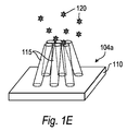
図1A〜図1Hは、様々なテント状構造要素100〜106を示し、各テント状構造要素は、テント状構造を形成するために複数(少なくとも2つ)のナノポール115を支持する基板110を含み、テント状構造は、本明細書において、図1Aに示されるように、ポールがそれぞれ、一方の端部115aで基板に取り付けられ、それらの他方の端部115bのそれらの先端で接触するように斜めに互いに傾いている構造として定義される。ナノポール、又は柱状体、又はフィンガ115の高さは、約50nm〜2μmの範囲内であり、それらの直径は約10nm〜1μmの範囲内である。
1A-1H show various tent-like structural elements 100-106, each tent-like structural element including a
図1Aは、テント構造100を形成するために先端部で接触している2つの係るナノポール115を示す。同様に、図1Bは構造101を形成する3つのナノポールを示す。図1Cは構造102を形成する4つのナノポールを示す。図1Dは構造103を形成する5つのナノポールを示す。図1E及び図1Fは、6つのナノポールを示し、2つの異なる構成において、それぞれ3つのナノポールからなる2つの平行な線(図1E)及び六角形の配置(図1F)がそれぞれ、構造104a及び104bを形成する。ナノポールの数が増加するにつれて、多角形、及び少なくとも2つの平行な線などのような様々な配置が、特定の配置におけるポールが全てそれらの先端部分115bの一部で接触する限り、使用され得る。図1Gは構造105を形成する7つのナノポールを示す。図1Hは構造106を形成する9つのナノポールを示す。図1A〜図1Hに示された配置は、単なる例示であり、ナノポールの他の構成、及びナノポールの他の数などが使用され得る。
FIG. 1A shows two
ナノポール115は本明細書で示されるように、断面を円形とすることができ、又はナノポールがそれらの先端部115bにおいて如何にして近寄るかを巧みに処理することを可能にすることができる、卵形のような非対称形状とすることができる。
The
各例において、ここで溶液(図示せず)の複数の分子120として表された被分析物は、一般にナノポール115の先端部115bにおいて又はその近くでナノポール115と関連付けられる(associated:結合される)。被分析物120は、基板110及びナノポール115にわたって分散され得るが、(1)ナノポールの表面にSERS活性金属(後述される)が存在すること、(2)レーザ照射の下で先端部に被分析物を集める傾向がある表面プラズモン効果に起因して、それらはナノポールの先端部115bと結合する可能性が高い。
In each example, an analyte, represented here as a plurality of
毛細管力(microcapillary force)は一般に、テント状構造要素100〜106を形成するために使用される。また、テント状構造要素100〜106の形成を生じさせるために、eビーム、イオンビーム、又は電気的荷電効果のような他の制限しない例も利用され得る。最初に形成されるナノポールは、3Dインプリンティング方法、型押し、CVD成長、エッチング、又はロールツーロール方式のような様々な技術により形成され得る垂直な自立型の柱である。 Capillary force is generally used to form the tent-like structural elements 100-106. Other non-limiting examples such as e-beams, ion beams, or electrical charging effects can also be utilized to cause the formation of tent-like structural elements 100-106. The first formed nanopole is a vertical freestanding column that can be formed by various techniques such as 3D imprinting methods, stamping, CVD growth, etching, or roll-to-roll systems.
次いで、構造要素100〜106は、水のような溶液内の被分析物にさらされる。乾燥時、毛細管力が、隣接するナノポール又は柱状体115を互いに引き寄せ、その結果、それらの先端部115bが接触する。このプロセスの間、被分析物120の分子は、隣接する柱状体115の間に捕捉される傾向がある。この場合、柱状体の先端部における柱状体の離隔距離は、分子のサイズに依存する。このプロセスは、構造要素100〜106の形成の十分に制御された均一性を提供する。
The structural elements 100-106 are then exposed to the analyte in a solution such as water. During drying, capillary forces pull adjacent nanopoles or
構造要素100〜106の形成は、柱状体をそれらの先端部で互いに保持するためのファンデルワールス相互作用に依存して、永久的にすることができると考えられる。これは、乾燥後、及び溶液に再度浸しても生じることができる。 It is believed that the formation of the structural elements 100-106 can be made permanent depending on the van der Waals interaction to hold the columns together at their tips. This can occur after drying and re-immersing in the solution.
他方では、構造要素100〜106の形成は、場合によっては元の垂直な自立型のナノポールに戻るように当該構造要素を後退させて開くように反発する電磁力、機械力、又は電荷を用いて可逆的にすることができる。 On the other hand, the formation of the structural elements 100-106 may be accomplished using electromagnetic force, mechanical force, or charge that repels the structural element back to open back to the original vertical freestanding nanopole. Can be reversible.
先端部におけるナノポール間の間隙に形成される強化(増強)された電磁界が存在する。電磁界強化の大きさは、間隙のサイズに依存し、それは上述したように、間隙に捕捉される分子のサイズに依存する。 There is an enhanced (enhanced) electromagnetic field formed in the gap between the nanopoles at the tip. The magnitude of the electromagnetic field enhancement depends on the size of the gap, which as described above depends on the size of the molecules trapped in the gap.
間隙のサイズが減少するにつれて、電磁界は増大する。例えば、間隙が2つの金属ナノ粒子間で10nmから1nm未満に減少する場合、電磁界では約1000倍の増大がある。SERS効果は、電磁界強化の4乗の関数であることが知られている。かくして、間隙が減少する際の103の増大は、ラマン信号強度において1012の改善という結果になる。 As the gap size decreases, the electromagnetic field increases. For example, if the gap decreases from 10 nm to less than 1 nm between two metal nanoparticles, there is an increase of about 1000 times in the electromagnetic field. The SERS effect is known to be a fourth power function of electromagnetic field enhancement. Thus, an increase of 10 3 as the gap decreases results in an improvement of 10 12 in Raman signal strength.
上述したように、間隙は、ほぼ分子のサイズ(捕捉された分子のサイズ)である。分子のサイズは、約1nm未満、一般的には約0.5nmであろう。 As described above, the gap is approximately the size of the molecule (the size of the captured molecule). The size of the molecule will be less than about 1 nm, typically about 0.5 nm.
チオ基(例えば−SH)が結合された炭素含有基を有する有機分子を考察する。この場合、これらチオ基は、ナノポール115を被覆する金属(例えば、金または銀)に結合することができる。かくして、約5nm、2〜3nm、1nm等の間隙のサイズが、分子のサイズ及び結合する基の存在に依存して得られることができる。
Consider an organic molecule having a carbon-containing group to which a thio group (eg, —SH) is attached. In this case, these thio groups can be bonded to the metal (eg, gold or silver) that coats the
ナノポールの数が大きくなればなるほど、捕捉され得る分子の数もより大きくなる。例えば、9つのナノポールは、2つ又は3つのナノポールに比べてより多くの分子を捕捉する。けれども、2つ又は3つのナノポールは、8つ又は9つのナノポールに比べて基板上の必要とする実面積が少ない。かくして、より多くのホットスポットの要望と、必要以上に高い密度が信号応答の減少という結果になるという事実との間になされるべきトレードオフが存在する。 The larger the number of nanopoles, the greater the number of molecules that can be captured. For example, nine nanopoles capture more molecules than two or three nanopoles. However, two or three nanopoles require less real area on the substrate than eight or nine nanopoles. Thus, there is a tradeoff to be made between the desire for more hot spots and the fact that higher density than necessary results in reduced signal response.
得られた構成100〜106は、以下で更に説明されるように、ナノポール115の最初の離隔距離により制御される。ナノポール115は、根元で測定される際に10〜500nmの範囲の距離だけ間隔を置いて配置され得る。
The resulting configurations 100-106 are controlled by the initial separation of the
図2Aは、ナノポール115のアレイ200の顕微鏡写真(平面図)であり、アレイの各ユニット210は、4つの係るナノポールからなる。各ユニット210における4つのナノポール115は、ナノポールの先端部がそれらの頂部で接触した状態で、ユニットの中心の方へ傾斜しているように看取される。
FIG. 2A is a photomicrograph (plan view) of an
図2Aにおいて、ナノポール115はそれぞれ、100nmの直径、及び100nmの離隔距離を有する。かくして、ピッチは200nmである。ナノポール115の高さは700nmである。
In FIG. 2A, the
図2Bは、ラマン強度(任意の単位)対ラマンシフト(cm−1)の座標におけるグラフであり、ナノインプリントリソグラフィーによりミラー上に形成された従来のランダムな円錐状のもの(コーン)に対する、それぞれ4つの柱状体(図2A)からなる多柱状構造要素のアレイからのラマン信号の強度の比較である。看取され得るように、本明細書で開示された構造は、ラマン信号の強度において大幅な増大を提供する。 FIG. 2B is a graph in the coordinates of Raman intensity (arbitrary units) versus Raman shift (cm −1 ), 4 for each of the conventional random cones (cones) formed on the mirror by nanoimprint lithography. 2 is a comparison of Raman signal intensities from an array of multi-columnar structural elements consisting of two columns (FIG. 2A). As can be seen, the structure disclosed herein provides a significant increase in the strength of the Raman signal.
図2Cは、図2Aに示された領域とは異なり、様々な構造要素という結果になったナノポール115の領域200’の拡大図である。特に、構造要素は、数ある中で4つのナノポール210a、6つのナノポール210b、及び9つのナノポール210cを含む。これは本質的に、同じサイズの構造要素の規則正しい分布を示す図2Aと比べて、異なるサイズの構造要素のランダムな分布である。上述したように、ナノポールの最初の離隔距離は、最後の所望の構成を制御するために使用され得る。ポールの隣接するグループ間の適切な離隔距離をグループ内のナノポール間の距離より僅かに大きくなるように選択することにより、最終的な構成の均一な制御につながることができる。
FIG. 2C is an enlarged view of region 200 'of
幾つかの実施形態において、ナノポールは、金、銀、銅、白金、アルミニウムなど、又は合金の形態でのこれら金属の組み合わせのようなSERS活性金属で被覆された、レジストのようなポリマーからなることができる。SERS活性金属は、ナノポール115全体にわたって被覆され得るか、又はナノポールの先端部115bに選択的に被覆され得る。更に、SERS活性金属は、多層構造とすることができる(例えば、1〜50nmの金の上側被覆を有する10〜100nmの銀の層、又は逆もまた同じである)。代案として、SERS活性金属は更に、薄い誘電体層で、又はALD成長された酸化ケイ素または酸化アルミニウム、酸化チタンなどのような機能的コーティングで被覆され得る。機能的コーティングは、被分析物の分子の選択的捕捉と検知を提供することができる。更に、プローブ種の自己組織化分子層が、ナノポールの先端部に形成され得る。
In some embodiments, the nanopole consists of a resist-like polymer coated with a SERS-active metal such as gold, silver, copper, platinum, aluminum, etc., or a combination of these metals in the form of an alloy. Can do. The SERS active metal can be coated throughout the
ポリマーの使用は、先端部が構造要素の頂部において接触するように曲がることを可能にするためにナノポールを十分にフレキシブルにする。適切なポリマーの例は、以下に限定されないが、ポリメタクリル酸メチル(PMMA)、ポリカーボネート、シロキサン、ポリジメチルシロキサン(PDMS)、フォトレジスト、ナノインプリントレジスト、並びに他の熱可塑性ポリマー及び1つ又は複数のモノマー/オリゴマー/ポリマーからなる紫外線硬化材料を含む。代案として、ナノポールは、曲がるのに十分な可撓性を有する無機材料からなることができる。係る無機材料の例は、酸化ケイ素、ケイ素(シリコン)、窒化ケイ素、アルミナ、ダイヤモンド、ダイヤモンド状炭素、アルミニウム、銅などを含む。 The use of a polymer makes the nanopole sufficiently flexible to allow the tip to bend to contact at the top of the structural element. Examples of suitable polymers include, but are not limited to, polymethyl methacrylate (PMMA), polycarbonate, siloxane, polydimethylsiloxane (PDMS), photoresist, nanoimprint resist, and other thermoplastic polymers and one or more Including UV curable material consisting of monomer / oligomer / polymer. Alternatively, the nanopole can be made of an inorganic material that is flexible enough to bend. Examples of such inorganic materials include silicon oxide, silicon (silicon), silicon nitride, alumina, diamond, diamond-like carbon, aluminum, copper and the like.
ナノポールの間隙の離隔距離は、調整(modulated:変調)され得る。熱で、又は特定の波長/パルスのレーザ下で試料を加熱することにより、ポール115の先端部の離隔間隙dは、微調整され得る。これは、構造要素の、異なるプラズモン特性を達成することを可能にする。図3Aは、ポール115の先端部が離隔距離d1を有する二ポール構造要素を示す。図3Bは、ポール115の先端部がd1と異なる(この場合、より大きい)離隔距離d2を有する類似した構造を示す。例えば、ゴムは20℃で〜10−4/℃の線形熱膨張を有する。従って、100nmの長さのゴム柱状体が10nmのd1を有していて20℃から120℃まで加熱される場合、離隔距離は、それぞれd1及びd2について10nmから約1nmまで変化することができる。当該プロセスは、温度が戻るように冷却される場合に可逆的にすることができる。
The separation distance of the nanopole gap can be modulated. By heating the sample with heat or under a specific wavelength / pulse laser, the gap d at the tip of the
同様に、適切な熱膨張または熱収縮が達成され得るようにナノポールの材料を設計することができる。例えば、2つの異なる材料を用いて、2つの異なる材料を加熱することから効果を得るようにナノポールを形成することができる。 Similarly, nanopole materials can be designed so that appropriate thermal expansion or contraction can be achieved. For example, nanopoles can be formed using two different materials to benefit from heating two different materials.
機械的曲げ、伸張/圧縮、又は基板の振動、電界または磁界のような他の手段を用いて構造を調整することもできる。特に、ナノポールが形成される基板は、PDMS又はゴム材料のようなエラストマー特性を有する材料とすることができる。伸張または圧縮力が基板に印加される場合、ポール先端部間の距離dは、例えば1nm未満のd1と5〜10nmのd2との間で調整され得る。 The structure can also be adjusted using mechanical bending, stretching / compression, or other means such as substrate vibration, electric or magnetic fields. In particular, the substrate on which the nanopole is formed can be a material having elastomeric properties such as PDMS or rubber material. When stretching or compressive force is applied to the substrate, the distance d between the pole tips can be adjusted, for example, between d 1 less than 1 nm and d 2 between 5 and 10 nm.
任意のテント状構造要素100〜106は、他の光学部品類と一体化され得る。例えば、図4Aは、金属ミラー402上に形成された三ポール構造要素400を示す。そして、金属ミラー402は、基板110上に形成される。金属ミラー402は、平面または凹面とすることができる。ミラー402を用いて光を構造要素400へ反射し、それにより信号強度の更なる増加を獲得することができる。
Optional tent-like structural elements 100-106 can be integrated with other optical components. For example, FIG. 4A shows a three pole
図4Bは、格子構造412上に形成された三ポール構造要素410を示す。そして、格子構造412は、基板110上に形成される。SERS構造と協働する格子構造は、他で説明されており、例えば米国特許第7,639,355号及び米国特許第7,474,396号を参照されたい。代案として、構造要素410自体が、格子として使用されてもよい。基板表面上で一次元または二次元に沿ってポールのピッチ又はテント状構造要素のピッチを適切に設計することにより、振幅変調干渉格子が確立され得る。
FIG. 4B shows a three
基板上にナノポールのアレイを製造する制限しない方法は、以下のことを含む。即ち、
1.Eビームリソグラフィ、フォトリソグラフィ、レーザ干渉リソグラフィ、FIB(集束イオンビーム)、球体の自己組織化などにより、モールド(型)上に所望のパターンを設計し、
2.シリコン基板、ガラス基板、ポリマー基板(PDMS、ポリイミド、ポリカーボネートなど)上へ当該パターンを転写し、
3.金、銀、銅などのようなラマン活性材料でナノポールを被覆し、
4.自己組織化を生じさせる(液体の乾燥でもってナノポールの先端部を互いに移動させる、即ち液体乾燥中の毛細管力が、規則的(例えば、図2A)又は不規則的(例えば、図2C)なテント状構造要素へのナノポールの自己組織化を生じさせる)。
Non-limiting methods of fabricating an array of nanopoles on a substrate include: That is,
1. E-beam lithography, photolithography, laser interference lithography, FIB (focused ion beam), self-organization of spheres, etc., design a desired pattern on the mold (mold),
2. Transfer the pattern onto a silicon substrate, glass substrate, polymer substrate (PDMS, polyimide, polycarbonate, etc.)
3. The nanopole is coated with a Raman active material such as gold, silver, copper, etc.
4). Tents that cause self-assembly (the nanopole tips move relative to each other with liquid drying, ie, capillary forces during liquid drying are regular (eg, FIG. 2A) or irregular (eg, FIG. 2C) Causing the self-organization of nanopoles into structural elements).
ナノポールのアセンブリのテント状構造要素の形成から得られる幾つかの利点が存在する。例えば、ナノポール(例えば、2つ、3つなど)の異なる幾何学的形状が、設計され得る。大きなSERS活性塊が、これら3D構造で達成され得る。プラズモン集束/結合が、テント状構造要素の先端部115bに向かって達成され得る。ミラー、格子などのような他の光学部品との容易な一体化が、容易に実現可能である。更に、特定の入射波長の下での最適なSERS性能のために、並びに蛍光、ルミネセンス(発光)、プラズモン共鳴、散乱などのような他の光学的検知のために、先端部の離隔距離の微調整が、熱またはレーザ加熱、機械力、電界または磁界を用いて可能である。
There are several advantages derived from the formation of tent-like structural elements of nanopole assemblies. For example, different geometric shapes of nanopoles (eg, 2, 3, etc.) can be designed. Large SERS active masses can be achieved with these 3D structures. Plasmon focusing / coupling can be achieved towards the
図5A〜図5Bは、本発明の実施形態に従って構成されて動作する被分析物センサの略図を示す。被分析物センサ500は、図1A〜図1Hに関連して上述されたような特徴要素504のアレイからなるラマン活性基板502、例えば光検出器506、及びラマン励起光源508を含む。
5A-5B show a schematic diagram of an analyte sensor constructed and operative in accordance with an embodiment of the present invention.
図5Aに示された例において、光源508は、ラマン励起光が特徴要素504(ナノポール115)のアレイに直接的に入射するように配置される。
In the example shown in FIG. 5A, the
図5Bに示された例において、光源508は、ラマン励起光が基板を通過するようにラマン活性基板502の下に配置される。この後者の場合、基板110は入射光に対して透過的とすることができる。
In the example shown in FIG. 5B, the
何れの場合も、光検出器506は、基板の表面の被分析物により放出されるラマン散乱光λemの少なくとも一部を捕捉するように配置される。
In any case, the
また、ラマン散乱光の強度は、ラマン活性材料に関連した2つのメカニズムの結果として強化され得る。第1のメカニズムは、ラマン活性基板502の表面、特に図1A〜図1Hに示されたナノポール115においてもたらされる強化された電磁界である。この結果、ナノアンテナ115の金属表面における伝導電子が、「表面プラズモンポラリトン」又は「局在表面プラズモン」と呼ばれる拡張表面励起電子状態へ励起される。ナノアンテナ115で又はその近傍で吸着された被分析物120は、比較的強い電磁界を受ける。ナノポール115の表面に垂直に向けられた分子振動モードが、最も強く強化される。表面プラズモンポラリトン共鳴の強度は、金属材料、アンテナ(ここでは、ナノポール115)のサイズ及び形状、並びに離隔距離を含む多くの要因に依存する。
Also, the intensity of the Raman scattered light can be enhanced as a result of two mechanisms associated with the Raman active material. The first mechanism is an enhanced electromagnetic field provided at the surface of the Raman
強化の第2のモード、電荷移動は、ナノポール115の表面とナノポール表面に吸収される被分析物120との間の電荷移動錯体の形成の結果として生じることができる。多くの電荷移動錯体の電子遷移は一般に、電磁スペクトルの可視範囲内にある。
A second mode of enhancement, charge transfer, can occur as a result of the formation of a charge transfer complex between the surface of the
上記の説明は、便宜上、SERS分析に関して提供された。しかしながら、理解されるように、同じ多柱状構造要素が、以下に限定されないが、増強蛍光、増強発光、及びプラズモン的検知、光学散乱および/または光吸収を含む他の解析技術に使用され得る。 The above description has been provided for SERS analysis for convenience. However, it will be appreciated that the same multi-columnar structural element can be used for other analytical techniques including, but not limited to, enhanced fluorescence, enhanced emission, and plasmonic detection, optical scattering and / or light absorption.
Claims (13)
少なくとも2つのナノポール(115)からなり、各ナノポールが一方の端部(115a)で基板(110)に取り付けられて、曲がるようにフレキシブルであり、前記少なくとも2つのナノポールの反対側の端部(115b)がそれぞれ、それらの反対側の端部において、溶液内の被分析物にさらされた後の乾燥時に毛細管力によって、前記被分析物の少なくとも1つの分子(120)を捕捉するように互いの方へ移動可能であり、各ナノポールが金属コーティングで被覆されている、多柱状構造要素(100〜106)。 A multi-columnar structural element (100 to 106) for molecular analysis,
It consists of at least two nanopoles (115), each nanopole is attached to the substrate (110) at one end (115a) and is flexible to bend , the opposite end (115b) of the at least two nanopoles ), respectively, at their ends opposite to the capillary force during drying after exposure to the analyte in solution, said to capture at least one molecular analyte (120) Multi-columnar structural elements (100 to 106) that are movable towards each other and each nanopole is coated with a metal coating.
前記アレイの各構造要素が、請求項1〜7の何れかに記載の構造要素からなる、多柱状構造要素のアレイ(200、200')。 An array of multi-columnar structural elements (200, 200 ') for molecular analysis,
An array of multi-columnar structural elements (200, 200 '), wherein each structural element of the array consists of the structural elements according to any of claims 1-7.
前記光検出器が、前記基板の、前記ナノポールと同じ側にあり、前記光源が、前記基板の、前記ナノポールと同じ側にあるか、又は前記基板の、前記ナノポールとは反対の側にある、請求項8に記載のアレイ。 For molecular analysis with a SERS device including a Raman excitation light source (508) and a photodetector (506),
The photodetector is on the same side of the substrate as the nanopole, and the light source is on the same side of the substrate as the nanopole, or on the opposite side of the substrate from the nanopole, The array according to claim 8.
前記基板上に複数の前記ナノポールを形成し、
各ナノポールに金属コーティングを施し、
前記複数のナノポールを溶液中の被分析物にさらし、
前記溶液を除去し、前記ナノポールに前記被分析物を残し、前記ナノポールの前記反対側の端部を、互いの方へ移動させて当該反対側の端部において前記被分析物の少なくとも1つの分子を捕捉することを含む、方法。 A method for creating a multi-columnar structural element according to claim 1,
Forming a plurality of the nanopoles on the substrate;
A metal coating to facilities in each Nanoporu,
Exposing the plurality of nanopoles to an analyte in solution;
Removing the solution, leaving the analyte on the nanopole, and moving the opposite ends of the nanopole towards each other to at least one molecule of the analyte at the opposite end Capturing the method.
Applications Claiming Priority (1)
| Application Number | Priority Date | Filing Date | Title |
|---|---|---|---|
| PCT/US2010/031790 WO2011133143A1 (en) | 2010-04-20 | 2010-04-20 | Multi-pillar structure for molecular analysis |
Publications (2)
| Publication Number | Publication Date |
|---|---|
| JP2013527921A JP2013527921A (en) | 2013-07-04 |
| JP5519075B2 true JP5519075B2 (en) | 2014-06-11 |
Family
ID=44834409
Family Applications (1)
| Application Number | Title | Priority Date | Filing Date |
|---|---|---|---|
| JP2013506118A Expired - Fee Related JP5519075B2 (en) | 2010-04-20 | 2010-04-20 | Multi-columnar structural elements for molecular analysis |
Country Status (5)
| Country | Link |
|---|---|
| US (1) | US20130040862A1 (en) |
| EP (1) | EP2561337A4 (en) |
| JP (1) | JP5519075B2 (en) |
| CN (1) | CN102834709A (en) |
| WO (1) | WO2011133143A1 (en) |
Cited By (2)
| Publication number | Priority date | Publication date | Assignee | Title |
|---|---|---|---|---|
| US9588048B2 (en) | 2011-05-20 | 2017-03-07 | Hewlett-Packard Development Company, L.P. | Surface enhanced raman spectroscopy sensor, system and method of sensing |
| US9594022B2 (en) | 2010-10-20 | 2017-03-14 | Hewlett-Packard Development Company, L.P. | Chemical-analysis device integrated with metallic-nanofinger device for chemical sensing |
Families Citing this family (26)
| Publication number | Priority date | Publication date | Assignee | Title |
|---|---|---|---|---|
| CN102947681B (en) * | 2010-04-20 | 2016-05-18 | 惠普发展公司,有限责任合伙企业 | Strengthen luminous automatic layout, luminous enhance device for surface |
| WO2012015443A1 (en) | 2010-07-30 | 2012-02-02 | Hewlett-Packard Development Company, L.P. | Optical fiber surface enhanced raman spectroscopy (sers) probe |
| US9274058B2 (en) | 2010-10-20 | 2016-03-01 | Hewlett-Packard Development Company, L.P. | Metallic-nanofinger device for chemical sensing |
| US9310306B2 (en) | 2011-02-17 | 2016-04-12 | Hewlett-Packard Development Company, L.P. | Apparatus for use in sensing applications |
| US9377409B2 (en) | 2011-07-29 | 2016-06-28 | Hewlett-Packard Development Company, L.P. | Fabricating an apparatus for use in a sensing application |
| US8520202B2 (en) | 2011-09-15 | 2013-08-27 | Hewlett-Packard Development Company, L.P. | Asymmetrical-nanofinger device for surface-enhanced luminescense |
| JP2013096939A (en) * | 2011-11-04 | 2013-05-20 | Seiko Epson Corp | Optical device and detector |
| US9574990B2 (en) | 2012-02-28 | 2017-02-21 | Hewlett-Packard Development Company, L.P. | SERS structures with nanoporous materials |
| WO2013158114A1 (en) | 2012-04-20 | 2013-10-24 | Hewlett-Packard Development Company, L.P. | Integrated sensors |
| US9453793B2 (en) | 2012-04-20 | 2016-09-27 | Hewlett-Packard Development Company, L.P. | Integrated sensors |
| EP2948757B1 (en) * | 2013-01-25 | 2017-04-26 | Hewlett-Packard Development Company, L.P. | Chemical sensing device |
| US9702821B2 (en) | 2013-01-30 | 2017-07-11 | Hewlett-Packard Development Company, L.P. | Surface enhanced fluorescence spectroscopy apparatus |
| US20140212867A1 (en) | 2013-01-30 | 2014-07-31 | Hewlett-Packard Development Company, L.P. | Device for monitoring and controlling cellular growth |
| JP2014160021A (en) * | 2013-02-20 | 2014-09-04 | Nsk Ltd | Target substance capturing device and target substance detection device including the same |
| US10520441B2 (en) * | 2013-03-14 | 2019-12-31 | Hewlett-Packard Development Company, L.P. | Devices to detect a substance and methods of producing such a device |
| CN105209910B (en) * | 2013-03-14 | 2019-02-15 | 百奥马克科技有限公司 | The detection of acetyl amantadine and quantitative in urine sample |
| DE102013008104A1 (en) * | 2013-05-14 | 2014-11-20 | Laser-Laboratorium Göttingen e.V. | SERS substrate |
| DE102013106432A1 (en) * | 2013-06-20 | 2014-12-24 | Endress + Hauser Conducta Gesellschaft für Mess- und Regeltechnik mbH + Co. KG | Optical indicator unit and device and method for determining a physico-chemical property of a process medium in a process plant |
| KR101448111B1 (en) * | 2013-09-17 | 2014-10-13 | 한국기계연구원 | A substrate for surface-enhanced Raman scattering spectroscopy and a preparing method thereof |
| EP3076161A1 (en) | 2015-04-01 | 2016-10-05 | Danmarks Tekniske Universitet | A substrate and a method of using it |
| KR101745080B1 (en) * | 2015-04-17 | 2017-06-09 | 연세대학교 산학협력단 | Manufacturing Method for Alumina Based Light Diffuser, and Light Diffuser Manufactured Thereby |
| CN105203511A (en) * | 2015-09-14 | 2015-12-30 | 东南大学 | Preparation method of substrate with fluorescence enhancement effect |
| US11402332B2 (en) | 2017-01-31 | 2022-08-02 | Hewlett-Packard Development Company, L.P. | Surface enhanced luminescence sensor nano finger |
| JP2017211395A (en) * | 2017-09-08 | 2017-11-30 | セイコーエプソン株式会社 | Raman spectrometer, raman spectroscopy, and electronic apparatus |
| KR102132624B1 (en) * | 2018-10-31 | 2020-07-10 | 연세대학교 산학협력단 | Substrate for raman scattering, method for manufacturing the same, analyzing apparatus and analyzing method comprising the same |
| WO2020091405A1 (en) * | 2018-10-30 | 2020-05-07 | 연세대학교 산학협력단 | Raman spectroscopy substrate and aptasensor |
Family Cites Families (9)
| Publication number | Priority date | Publication date | Assignee | Title |
|---|---|---|---|---|
| WO2002093738A2 (en) * | 2001-01-19 | 2002-11-21 | California Institute Of Technology | Carbon nanobimorph actuator and sensor |
| WO2002093140A1 (en) * | 2001-05-14 | 2002-11-21 | Johns Hopkins University | Multifunctional magnetic nanowires |
| US6970239B2 (en) * | 2002-06-12 | 2005-11-29 | Intel Corporation | Metal coated nanocrystalline silicon as an active surface enhanced Raman spectroscopy (SERS) substrate |
| US7163659B2 (en) * | 2002-12-03 | 2007-01-16 | Hewlett-Packard Development Company, L.P. | Free-standing nanowire sensor and method for detecting an analyte in a fluid |
| JP2006145230A (en) * | 2004-11-16 | 2006-06-08 | Canon Inc | Specimen carrier and its manufacturing method |
| US7245370B2 (en) * | 2005-01-06 | 2007-07-17 | Hewlett-Packard Development Company, L.P. | Nanowires for surface-enhanced Raman scattering molecular sensors |
| US7940387B2 (en) * | 2005-03-15 | 2011-05-10 | Univeristy Of Georgia Research Foundation, Inc. | Surface enhanced Raman spectroscopy (SERS) systems for the detection of viruses and methods of use thereof |
| US7528948B2 (en) * | 2006-07-25 | 2009-05-05 | Hewlett-Packard Development Company, L.P. | Controllable surface enhanced Raman spectroscopy |
| US7898658B2 (en) * | 2007-01-23 | 2011-03-01 | The Regents Of The University Of California | Platform for chemical and biological sensing by surface-enhanced Raman spectroscopy |
-
2010
- 2010-04-20 CN CN2010800663207A patent/CN102834709A/en active Pending
- 2010-04-20 JP JP2013506118A patent/JP5519075B2/en not_active Expired - Fee Related
- 2010-04-20 US US13/636,799 patent/US20130040862A1/en not_active Abandoned
- 2010-04-20 WO PCT/US2010/031790 patent/WO2011133143A1/en active Application Filing
- 2010-04-20 EP EP10850365.7A patent/EP2561337A4/en not_active Withdrawn
Cited By (2)
| Publication number | Priority date | Publication date | Assignee | Title |
|---|---|---|---|---|
| US9594022B2 (en) | 2010-10-20 | 2017-03-14 | Hewlett-Packard Development Company, L.P. | Chemical-analysis device integrated with metallic-nanofinger device for chemical sensing |
| US9588048B2 (en) | 2011-05-20 | 2017-03-07 | Hewlett-Packard Development Company, L.P. | Surface enhanced raman spectroscopy sensor, system and method of sensing |
Also Published As
| Publication number | Publication date |
|---|---|
| WO2011133143A1 (en) | 2011-10-27 |
| EP2561337A4 (en) | 2013-12-25 |
| JP2013527921A (en) | 2013-07-04 |
| CN102834709A (en) | 2012-12-19 |
| US20130040862A1 (en) | 2013-02-14 |
| EP2561337A1 (en) | 2013-02-27 |
Similar Documents
| Publication | Publication Date | Title |
|---|---|---|
| JP5519075B2 (en) | Multi-columnar structural elements for molecular analysis | |
| US8993339B2 (en) | Hybrid nanostructures for molecular analysis | |
| Kanipe et al. | Large format surface-enhanced Raman spectroscopy substrate optimized for enhancement and uniformity | |
| RU2361193C2 (en) | Optical sensor with multilayered plasmon structure for improved detection of chemical groups through sers | |
| US9176065B2 (en) | Nanoscale array structures suitable for surface enhanced raman scattering and methods related thereto | |
| Lal et al. | Tailoring plasmonic substrates for surface enhanced spectroscopies | |
| Yan et al. | Engineered SERS substrates with multiscale signal enhancement: nanoparticle cluster arrays | |
| US8462334B2 (en) | Sensor system with plasmonic nano-antenna array | |
| Liu et al. | Flexible three-dimensional anticounterfeiting plasmonic security labels: Utilizing z-axis-dependent SERS readouts to encode multilayered molecular information | |
| Song et al. | Partial leidenfrost evaporation-assisted ultrasensitive surface-enhanced Raman spectroscopy in a Janus water droplet on hierarchical plasmonic micro-/nanostructures | |
| Tripathy et al. | Acousto-plasmonic and surface-enhanced Raman scattering properties of coupled gold nanospheres/nanodisk trimers | |
| Sow et al. | Revisiting surface-enhanced Raman scattering on realistic lithographic gold nanostripes | |
| Kravets et al. | Composite Au nanostructures for fluorescence studies in visible light | |
| JP2009042112A (en) | Sensing device and sensing method using it |
Legal Events
| Date | Code | Title | Description |
|---|---|---|---|
| A977 | Report on retrieval |
Free format text: JAPANESE INTERMEDIATE CODE: A971007 Effective date: 20131003 |
|
| A521 | Written amendment |
Free format text: JAPANESE INTERMEDIATE CODE: A523 Effective date: 20140203 |
|
| TRDD | Decision of grant or rejection written | ||
| A01 | Written decision to grant a patent or to grant a registration (utility model) |
Free format text: JAPANESE INTERMEDIATE CODE: A01 Effective date: 20140304 |
|
| A61 | First payment of annual fees (during grant procedure) |
Free format text: JAPANESE INTERMEDIATE CODE: A61 Effective date: 20140402 |
|
| R150 | Certificate of patent or registration of utility model |
Ref document number: 5519075 Country of ref document: JP Free format text: JAPANESE INTERMEDIATE CODE: R150 |
|
| LAPS | Cancellation because of no payment of annual fees |