EP3551931B1 - Wellenleiter mit peripheren seitengeometrien zum recyceln von licht - Google Patents
Wellenleiter mit peripheren seitengeometrien zum recyceln von licht Download PDFInfo
- Publication number
- EP3551931B1 EP3551931B1 EP17829739.6A EP17829739A EP3551931B1 EP 3551931 B1 EP3551931 B1 EP 3551931B1 EP 17829739 A EP17829739 A EP 17829739A EP 3551931 B1 EP3551931 B1 EP 3551931B1
- Authority
- EP
- European Patent Office
- Prior art keywords
- coupler
- optical waveguide
- peripheral side
- output
- waveguide
- Prior art date
- Legal status (The legal status is an assumption and is not a legal conclusion. Google has not performed a legal analysis and makes no representation as to the accuracy of the status listed.)
- Active
Links
Images


Classifications
-
- G—PHYSICS
- G02—OPTICS
- G02B—OPTICAL ELEMENTS, SYSTEMS OR APPARATUS
- G02B27/00—Optical systems or apparatus not provided for by any of the groups G02B1/00 - G02B26/00, G02B30/00
- G02B27/01—Head-up displays
- G02B27/017—Head mounted
- G02B27/0172—Head mounted characterised by optical features
-
- G—PHYSICS
- G02—OPTICS
- G02B—OPTICAL ELEMENTS, SYSTEMS OR APPARATUS
- G02B27/00—Optical systems or apparatus not provided for by any of the groups G02B1/00 - G02B26/00, G02B30/00
- G02B27/0081—Optical systems or apparatus not provided for by any of the groups G02B1/00 - G02B26/00, G02B30/00 with means for altering, e.g. enlarging, the entrance or exit pupil
-
- G—PHYSICS
- G02—OPTICS
- G02B—OPTICAL ELEMENTS, SYSTEMS OR APPARATUS
- G02B6/00—Light guides; Structural details of arrangements comprising light guides and other optical elements, e.g. couplings
- G02B6/0001—Light guides; Structural details of arrangements comprising light guides and other optical elements, e.g. couplings specially adapted for lighting devices or systems
- G02B6/0011—Light guides; Structural details of arrangements comprising light guides and other optical elements, e.g. couplings specially adapted for lighting devices or systems the light guides being planar or of plate-like form
- G02B6/0013—Means for improving the coupling-in of light from the light source into the light guide
- G02B6/0015—Means for improving the coupling-in of light from the light source into the light guide provided on the surface of the light guide or in the bulk of it
- G02B6/002—Means for improving the coupling-in of light from the light source into the light guide provided on the surface of the light guide or in the bulk of it by shaping at least a portion of the light guide, e.g. with collimating, focussing or diverging surfaces
-
- G—PHYSICS
- G02—OPTICS
- G02B—OPTICAL ELEMENTS, SYSTEMS OR APPARATUS
- G02B27/00—Optical systems or apparatus not provided for by any of the groups G02B1/00 - G02B26/00, G02B30/00
- G02B27/01—Head-up displays
- G02B27/0101—Head-up displays characterised by optical features
- G02B2027/0123—Head-up displays characterised by optical features comprising devices increasing the field of view
- G02B2027/0125—Field-of-view increase by wavefront division
-
- G—PHYSICS
- G02—OPTICS
- G02B—OPTICAL ELEMENTS, SYSTEMS OR APPARATUS
- G02B27/00—Optical systems or apparatus not provided for by any of the groups G02B1/00 - G02B26/00, G02B30/00
- G02B27/01—Head-up displays
- G02B27/017—Head mounted
- G02B2027/0178—Eyeglass type
-
- G—PHYSICS
- G02—OPTICS
- G02B—OPTICAL ELEMENTS, SYSTEMS OR APPARATUS
- G02B6/00—Light guides; Structural details of arrangements comprising light guides and other optical elements, e.g. couplings
- G02B6/0001—Light guides; Structural details of arrangements comprising light guides and other optical elements, e.g. couplings specially adapted for lighting devices or systems
- G02B6/0011—Light guides; Structural details of arrangements comprising light guides and other optical elements, e.g. couplings specially adapted for lighting devices or systems the light guides being planar or of plate-like form
- G02B6/0033—Means for improving the coupling-out of light from the light guide
- G02B6/0035—Means for improving the coupling-out of light from the light guide provided on the surface of the light guide or in the bulk of it
Definitions
- Various types of computing, entertainment, and/or mobile devices can be implemented with a transparent or semi-transparent display through which a user of a device can view the surrounding environment.
- Such devices which can be referred to as see-through, mixed reality display device systems, or as augmented reality (AR) systems, enable a user to see through the transparent or semi-transparent display of a device to view the surrounding environment, and also see images of virtual objects (e.g., text, graphics, video, etc.) that are generated for display to appear as a part of, and/or overlaid upon, the surrounding environment.
- virtual objects e.g., text, graphics, video, etc.
- HMD head-mounted display
- These devices which can be implemented as head-mounted display (HMD) glasses or other wearable display devices, but are not limited thereto, often utilize optical waveguides to replicate an image, e.g., produced by a display engine, to a location where a user of a device can view the image as a virtual image in an augmented reality environment.
- an image e.g., produced by a display engine
- a user of a device can view the image as a virtual image in an augmented reality environment.
- waveguides to display images of virtual objects to a user.
- WO2016006758A1 teaches a lightguide structure comprising: a first portion disposed to receive light rays emitted by an external display, a second portion disposed to provide, to a second surface facing a viewer, the light rays from the first portion and ambient light, wherein the second portion has a plurality of first surfaces for reflecting light rays and at least one second surface which the light rays and the ambient light perpendicularly enter into and pass through, an intermediate portion disposed to connect between the first portion and the second portion and reflect the light rays from the first portion for transferring the light rays to the second portion.
- US20120206817A1 teaches that a thickness of a tapered part provided at the deeper side in a light guide direction of a light transmission member is smaller toward the deeper side, and thus, a reflection angle of ghost light that has passed through a fourth reflection surface provided with a half mirror layer and reached the light transmission member gradually becomes smaller within the tapered part and no longer satisfies a total reflection condition, and the light is ejected to the outside in the position diverging from an eye of an observer.
- a half mirror layer has an angle dependency in which when an angle of incidence becomes larger than the angle of incidence range of image light, reflectance increases, such that it is possible to prevent unintended light, which is emitted to a light transmitting member from a light guiding member and is reflected inside a light transmitting member, from being returned to a light emission portion of the light guiding member after passing through the half mirror layer as a reflective film at a relatively large angle of incidence.
- US6563992B1 teaches a fiber-optic coupled diffuse reflectance probe that is adapted to detachably connect to a bifurcated fiber bundle.
- WO2012066798A1 teaches that a three-dimensional display device, the occurrence of crosstalk is suppressed.
- Left-side light sources and right-side light sources are respectively disposed facing the light entrance end surfaces of light guide plates.
- the end surfaces at the reverse side from the light entrance end surfaces of the light guide plates are inclined, forming inclined surfaces.
- Light absorption members are provided to the region facing the inclined surfaces at the front surface or rear surface of the light guide plates.
- an apparatus for use in replicating an image associated with an input-pupil to an output-pupil.
- Such an apparatus comprises an optical waveguide including a bulk-substrate, an input-coupler and an output-coupler.
- the bulk-substrate of the optical waveguide includes a first major side, a second major side opposite the first major side, and peripheral sides that can extend between the first and second major sides.
- the input-coupler of the optical waveguide is configured to couple, into the bulk-substrate of the optical waveguide, light corresponding to the image associated with the input-pupil.
- the output-coupler of the optical waveguide is configured to couple, out of the bulk-substrate of the optical waveguide, light corresponding to the image that has traveled through the optical waveguide from the input-coupler to the output-coupler at least in part by way of total internal reflection (TIR).
- TIR total internal reflection
- At least one of the peripheral sides of the bulk-substrate of the optical waveguide includes first and second surfaces that define first and second planes angled 45 degrees relative to one another. Such a peripheral side provides for effective recycling of light that may otherwise undesirably leak out of optical waveguide through the peripheral side.
- Certain embodiments of the present technology relate to apparatuses for use in replicating an image associated with an input-pupil to an output-pupil.
- Such apparatuses can include a waveguide.
- waveguides are used to perform pupil replication (also referred to as image replication)
- light may inadvertently and undesirably leak out of the waveguide through one or peripheral sides of the waveguide. This may degrade the optical efficiency of the waveguide and may cause undesirable stray light in a system that includes the waveguide.
- Certain embodiments described herein can be used to reduce and preferably prevent light from inadvertently and undesirably leaking out of an optical waveguide through its peripheral sides, and thereby, can be used to improve the optical efficiency of the waveguide and reduce and preferably prevent stray light within a system that includes the waveguide.
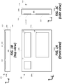
- FIGS. 1A, 1B and 1C are front, top and side views, respectively, of an exemplary optical waveguide 100 that can be used to replicate an image associated with an input-pupil to an expanded output-pupil.
- the term "input-pupil,” as used herein, refers to an aperture through which light corresponding to an image is overlaid on an input-coupler of a waveguide.
- An input-pupil is sometimes also referred to as an entrance-pupil
- an output-pupil is sometimes also referred to as an exit-pupil.
- the optical waveguide 100 will often be referred to hereafter more succinctly simply as a waveguide 100.
- the image that the waveguide 100 is being used to replicate, and likely also expand, can be generated using a display engine.
- the optical waveguide 100 includes a bulk-substrate 106 having an input-coupler 112 and an output-coupler 116.
- the input-coupler 112 is configured to couple light corresponding to an image associated with an input-pupil into the bulk-substrate 106 of the waveguide.
- the output-coupler 116 is configured to couple the light corresponding to the image associated with the input-pupil, which travels in the optical waveguide 100 from the input-coupler 112 to the output-coupler 116, out of the waveguide 100 so that the light is output and viewable from the output-pupil.
- the bulk-substrate 106 which can be made of glass or optical plastic, but is not limited thereto, includes a first major side 108, a second major side 110, and peripheral sides 109a, 109b, 109c and 109d.
- the first major side 108 and the second major side 110 are opposite and parallel to one another.
- the major sides 108 and 110 are planar.
- the major sides 108 and 110 are curved.
- the first major side 108 can alternatively be referred to as the front-side 108
- the second major side 110 can alternatively be referred to as the back-side 110.
- peripheral sides 109a, 109b, 109c and 109d can be referred to individually as a peripheral side 109, or collectively as the peripheral sides 109.
- a substrate is considered to be “bulk” substrate where the thickness of the substrate (between its major sides) is at least ten times (i.e., 10x) the wavelength of the light for which the substrate is being used as an optical transmission medium.
- the substrate will be considered a bulk-substrate where the thickness of the substrate (between its major sides) is at least 6200 nm, i.e., at least 6.2 ⁇ m.
- the bulk-substrate 106 has a thickness of at least 25 ⁇ m between its major sides 108 and 110.
- the bulk-substrate 106 has a thickness (between its major sides) within a range of 25 ⁇ m to 1000 ⁇ m.
- the bulk-substrate 106, and more generally the waveguide 100 is transparent, meaning that it allows light to pass through it so that a user can see through the waveguide 100 and observe objects on an opposite side of the waveguide 100 than the user's eye(s).
- the optical waveguide 100 in FIGS. 1A, 1B and 1C is also shown as including an intermediate-component 114, which can alternatively be referred to as an intermediate-zone 114.
- the input-coupler 112 is configured to couple light into the waveguide 100 (and more specifically, into the bulk-substrate 106 of the waveguide 100) and in a direction of the intermediate-component 114.
- the intermediate-component 114 is configured to redirect such light in a direction of the output-coupler 116.
- the intermediate-component 114 is configured to perform one of horizontal or vertical pupil expansion
- the output-coupler 116 is configured to perform the other one of horizontal or vertical pupil expansion.
- the intermediate-component 114 can be configured to perform horizontal pupil expansion, and the output-coupler 116 can be configured to vertical pupil expansion.
- the intermediate-component 114 were repositioned, e.g., to be below the input-coupler 112 and to the left of the output-coupler 116 shown in FIG. 1A , then the intermediate-component 114 can be configured to perform vertical pupil expansion, and the output-coupler 116 can be configured to perform horizontal pupil expansion.
- the input-coupler 112, the intermediate-component 114 and the output-coupler 116 can be referred to collectively herein as optical components 112, 114 and 116 of the waveguide, or more succinctly as components 112, 114 and 116.
- a waveguide includes an input-coupler and an output-coupler, without including an intermediate-components.
- the input-coupler would be configured to couple light into the waveguide and in a direction toward the output-coupler.
- the output-coupler can provide one of horizontal or vertical pupil expansion, depending upon implementation.
- the input-coupler 112, the intermediate-component 114 and the output-coupler 116 are shown as having rectangular outer peripheral shapes, but can have alternative outer peripheral shapes.
- the input-coupler 112 can alternatively have a circular outer peripheral shape, but is not limited thereto.
- the intermediate-component can have a triangular or hexagonal outer peripheral shape, but is not limited thereto.
- the corners of each of the peripheral shapes e.g., where generally rectangular or triangular, can be chamfered or rounded, but are not limited thereto.
- the input-coupler 112, the intermediate-component 114 and the output-coupler 116 are all shown as being provided in or on a same side (i.e., the back-side 110) of the waveguide 100.
- the input-coupler 112 can be transmissive (e.g., a transmission grating)
- the intermediate-component 114 can be reflective (e.g., a reflective grating)
- the output-coupler 116 can also be reflective (e.g., a further reflective grating).
- the input-coupler 112, the intermediate-component 114 and the output-coupler 116 can alternatively all be provided in the front-side 110 of the waveguide 100.
- the input-coupler 112 can be reflective (e.g., a reflective grating)
- the intermediate-component 114 can be reflective (e.g., a further reflective grating)
- the output-coupler 116 can also be transmissive (e.g., a transmission grating).
- the input-coupler 112, the intermediate-component 114 and the output-coupler 116 can all be embedded (also referred to as immersed) in the bulk-substrate 106.
- the bulk-substrate 106 can be separated into two halves (that are parallel to the major sides 108 and 110), and the input-coupler 112, the intermediate-component 114 and the output-coupler 116 can be provided in (e.g., etched into) one of the inner surfaces of the two halves, and the inner surfaces of the two halves can be adhered to one another.
- the bulk-substrate 106 can be separated into two halves (that are parallel to the major sides 108 and 110), and the input-coupler 112, the intermediate-component 114 and the output-coupler 116 can be provided between the inner surfaces of the two halves.
- Other implementations for embedding the input-coupler 112, the intermediate-component 114 and the output-coupler 116 in the bulk-substrate 106 are also possible, and within the scope of the embodiments described herein.
- one of the input-coupler 112, the intermediate-component 114 and the output-coupler 116 is provided in or on the front-side 108 of the waveguide 108, another one of the components 112, 114 and 116 is provided in or on the back-side 110, and the last one of the components 112, 114 and 116 is embedded or immersed in the bulk-substrate 106. More generally, unless stated otherwise, any individual one of the input-coupler 112, the intermediate-component 114 and the output-coupler 116 can be provided in or on either one of the major sides 108 or 110 of the bulk-substrate 106, or embedded therebetween.
- the input-coupler 112, the intermediate-component 114 and the output-coupler 116 can each be implemented as a diffraction grating, or more generally, as a diffractive optical element (DOE).
- DOE diffractive optical element
- a diffraction grating is an optical component that may contain a periodic structure that causes incident light to split and change direction due to an optical phenomenon known as diffraction. The splitting (known as optical orders) and angle change depend on the characteristics of the diffraction grating.
- the periodic structure is on the surface of an optical component, it is referred to a surface grating.
- SRG surface relief grating
- an SRG can include uniform straight grooves in a surface of an optical component that are separated by uniform straight groove spacing regions. Groove spacing regions can be referred to as "lines", “grating lines” or “filling regions”. The nature of the diffraction by an SRG depends on the wavelength, polarization and angle of light incident on the SRG and various optical characteristics of the SRG, such as refractive index (also known as the index of refraction), line spacing, groove depth, groove profile, groove fill ratio and groove slant angle.
- refractive index also known as the index of refraction
- An SRG can be fabricated by way of a suitable microfabrication process, which may involve etching of and/or deposition on a substrate to fabricate a desired periodic microstructure on the substrate to form an optical component, which may then be used as a production master such as a mold or mask for manufacturing further optical components.
- An SRG is an example of a Diffractive Optical Element (DOE).
- DOE Diffractive Optical Element
- a diffraction grating instead of being a surface grating, can alternatively be a volume grating, such as a Bragg diffraction grating.
- one or more of the couplers are manufactured as SRGs and then covered within another material, e.g., using an aluminum deposition process, thereby essentially burying the SRGs such that the major waveguide surface(s) including the SRG(s) is/are substantially smooth.
- a coupler is one example of a hybrid of a surface and volume diffraction grating.
- Any one of the input-coupler 112, the intermediate-component 114 and the output-coupler 116 can be, e.g., a surface diffraction grating, or a volume diffraction grating, or a hybrid of a surface and volume diffraction grating.
- Each diffraction grating can have a preferential linear polarization orientation specified by a direction of the grating lines of the diffraction grating, wherein the coupling efficiency for light having the preferential linear polarization orientation will be higher than for light having a non-preferential linear polarization orientation.
- each such SRG can be etched into one of the major sides 108 or 110 of the bulk-substrate 106.
- the SRG can be said to be formed "in” the bulk-substrate 106.
- each SRG can be physically formed in a coating that covers one of the major sides 108 or 110 of the bulk-substrate 106, in which case each such SRG can be said to be formed "on” the bulk-substrate 106.
- the components 112, 114 and 116 are considered parts of the waveguide 100.
- the input-coupler 112 can have surface gratings that extend in a vertical (y) direction
- the output-coupler 116 can have surface gratings that extend in a horizontal (x) direction
- the intermediate-component 114 can have surface gratings that extend diagonal (e.g., ⁇ 45 degrees) relative to the horizontal and vertical directions. This is just an example. Other variations are also possible.
- the input-coupler 112, the intermediate-component 114 and the output-coupler 116 can have various different outer peripheral geometries, can be provided in or on either of the major sides of the bulk-substrate, or can be embedded in the bulk-substrate 106, and can be implemented using various different types of optical structures, as can be appreciated from the above discussion, and will further be appreciated from the discussion below.
- TIR total internal refection
- FIG. 2 shows a side view of the waveguide 100, but also shows a display engine 204 that generates an image including angular content that is coupled into the waveguide by the input-coupler 112. Also shown in FIG. 2 , is representation of a human eye 214 that is using the waveguide 100 to observe an image, produced using the display engine 204, as a virtual image.
- the display engine 204 can include, e.g., an image former 206, a collimating lens 208 and an illuminator 210, but is not limited thereto.
- the image former 206 can be implemented using a transmissive projection technology where a light source is modulated by an optically active material, and backlit with white light. These technologies are usually implemented using liquid crystal display (LCD) type displays with powerful backlights and high optical energy densities.
- the illuminator 210 can provide the aforementioned backlighting.
- the image former 206 can also be implemented using a reflective technology for which external light is reflected and modulated by an optically active material. Digital light processing (DLP), liquid crystal on silicon (LCOS) and Mirasol(TM) display technology from Qualcomm, Inc.
- DLP digital light processing
- LCOS liquid crystal on silicon
- Mirasol(TM) display technology from Qualcomm, Inc.
- the image former 206 can be implemented using an emissive technology where light is generated by a display, see for example, a PicoP(TM) display engine from Microvision, Inc.
- a PicoP(TM) display engine from Microvision, Inc.
- Another example of emissive display technology is a micro organic light emitting diode (OLED) display. Companies such as eMagin(TM) and Microoled(TM) provide examples of micro OLED displays.
- the image former 206 alone or in combination with the illuminator 210, can also be referred to as a micro display.
- the collimating lens 208 is arranged to receive a diverging display image from the image former 206, to collimate the display image, and to direct the collimated image toward the input-coupler 112 of the waveguide 100.
- an entry pupil associated with the waveguide may be approximately the same size as an exit pupil associated with the image former 206, e.g., 5 mm or less in some embodiments, but is not limited there
- the display engine 204 is shown as facing the back-side 110 of the waveguide 100, and the eye 214 is shown as facing the front-side 108 opposite and parallel to the back-side 110.
- This provides for a periscope type of configuration in which light enters the waveguide on one side of the waveguide 100, and exits the waveguide at an opposite side of the waveguide 100.
- the input-coupler 112 and the output-coupler 116 can be implemented in a manner such that the display engine 204 and the eye 214 are proximate to and face a same major side (108 or 110).
- the waveguide 100 can be incorporated into a see-through mixed reality display device system, but is not limited to use therewith.
- a separate instance of the waveguide 100 and the display engine 204 can be provided for each of the left and right eyes of a user.
- such waveguide(s) 100 may be positioned next to or between see-through lenses, which may be standard lenses used in eye glasses and can be made to any prescription (including no prescription).
- a see-through mixed reality display device system is implemented as head-mounted display (HMD) glasses including a frame
- the display engine 204 can be located to the side of the frame so that it sits near to a user's temple.
- the display engine 204 can be located in a central portion of the HMD glasses that rests above a nose bridge of a user. Other locations for the display engine 204 are also possible. In these instances, the user can also be referred to as a wearer. Where there is a separate waveguide for each of the left and right eyes of a user, there can be a separate display engine for each of the waveguides, and thus, for each of the left and right eyes of the user. One or more further adjacent waveguides can be used to perform eye tracking based on infrared light that is incident on and reflected from the user's eye(s) 214, as is known in the art.
- light that is coupled into the waveguide 100 by the input-coupler 112 can travel by way of TIR from the input-coupler 112 to the intermediate-component 114, and by way of TIR from the intermediate-component 114 to the output-coupler 116, where it exits the waveguide 100.
- a combination of diffractive beam splitting and TIR within the waveguide 100 results in multiple versions of an input beam of light being outwardly diffracted from the output-coupler 116 in both the length and the width of the output-coupler 116.
- some light that is coupled into the waveguide 100, after traveling in a propagation direction towards the output-coupler 116 may not be coupled out of the waveguide 100 by the output-coupler 116, and thus, may reach the peripheral side 109d and eventually leak out of the waveguide 100 through the peripheral side 109d. This may degrade the optical efficiency of the waveguide 100 and may cause undesirable stray light in a system that includes the waveguide 100. Similarly, light may undesirably leak out one or more of the other peripheral sides 109a, 109b and/or 109c.
- optical efficiency of a waveguide refers to the amount of light that is coupled into the waveguide through an input-coupler of the waveguide divided by the amount of light that is coupled out of the waveguide through an output-coupler of the waveguide.
- the portion of the light that leaks out through the peripheral side 109d is labelled 222.
- the light 222 that leaks out of the peripheral side 109d is shown as continuing with a same angle that the light had when it was incident on the peripheral side, but this angle would likely actually be altered due to differences between the index of refraction of the bulk substrate 106 of the waveguide and the air or other medium adjacent to the peripheral side 109d.
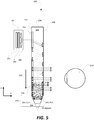
- One technique to improve the optical efficiency of the waveguide 100 is to coat one or more of the peripheral sides 109 with a reflective material, as shown in FIG. 3 . More specifically, in FIG. 3 , the peripheral side 109d is shown as being coated with a reflective material 302, which can also be referred to as a reflective coating 302. Exemplary materials that may be used as the reflective coating include, but are not limited to, aluminium, gold, silver, a gold-alloy or a silver-alloy, or a dielectric material such as magnesium fluoride, or a combination thereof.
- the reflective coating 302 will cause light traveling within the waveguide 100 that reaches the peripheral side 109d (that is coated with the reflective coating 302) to be reflected off of the peripheral side 109d in the opposite direction.
- Rays of light that are reflected off the reflectively coated peripheral side 109d can be referred to as recycled light. If the reflectively coated peripheral side 109d is precisely 90 degrees relative to the major sides 108 and 110, then the recycled light will have the same angle of incidence relative to the major sides 108 and 110 that the light had when it was incident on the reflectively coated peripheral side 109d.
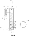
- a problem is that if the reflectively coated completely planar peripheral side 109d is not precisely 90 degrees relative to the major sides 108 and 110, then ghost images may result, as will be explained in more detail with reference to FIG. 4 .
- peripheral side 109 Due to manufacturing tolerances, it is very difficult to manufacture a peripheral side 109 such that it is precisely 90 degrees relative to the major sides 108 and 110. The adverse effects of a peripheral side 109 not being precisely 90 degrees relative to the major sides 108 and 110 will now be described with reference to FIG. 4 .
- the peripheral side 109d which is shown as not being precisely 90 degrees relative to the major sides 108 and 110, is coated with the reflective coating 302.
- the reflective coating 302 will cause light traveling within the waveguide 100 that reaches the peripheral side 109d (that is coated with the reflective coating 302) to be reflected off of the peripheral side 109d in the opposite direction. Rays of light that are reflected off the reflectively coated peripheral side 109d, which are shown in slightly thicker lines and are labelled 404, can be referred to as recycled light. As shown in FIG.
- the recycled light 404 will have a different angle of incidence relative to the major sides 108 and 110 than the light had when it was incident on the reflectively coated peripheral side 109d. This will result in the recycled light being diffracted out of the output-coupler 116 at a different angle than the light would have been diffracted out of the output-coupler 116 prior to being incident on the reflectively coated peripheral side 109d. This will result in an undesirable ghost image of a virtual image presented to a user's eye by the optical waveguide. Such a ghost image is essentially a replica of the desired virtual image that is offset in position and super imposed on top of the desired virtual image. Certain embodiments of the present technology, which are described below, effectively recycle light without causing such ghost images.
- FIG. 5 is a side view of a waveguide 100 including a peripheral side 109d having a geometry that effectively recycles light, according to an example of the present technology.
- the peripheral side 109d is shown as including surfaces 502 and 504 that define first and second planes 512 and 514 which are angled 45 degrees relative to one another.
- the peripheral side 109d (which includes the surfaces 502 and 504 that define first and second planes 512 and 514 angled 45 degrees relative to one another) is configured to recycle light (corresponding to an image) that is incident on the peripheral side 109d after traveling within the bulk-substrate 106 of the optical waveguide 100 in a propagation direction toward the peripheral side 109d.
- the peripheral side 109d is also shown as including a surface 506 that extends between the surfaces 502 and 504. Accordingly, in FIG. 5 edges between the peripheral side 109d and the first and second major planar sides 108 and 110 are chamfered edges. In an alternative example, the surfaces 502 and 504 of the peripheral side 109d meet one another at a 45 degree angle, and thus, there is no surface 506. In such an alternative example, the edges between the peripheral side and the first and second major planar sides are bevelled edges.
- the surface 502 is a planar surface that is coextensive with the first plane 512
- the surface 504 is a planar surface that is coextensive with the second plane 514.
- the surface 502 and the first plane 512 are equivalent to one another
- the surface 504 and the second plane 514 are equivalent to one another.
- the propagation direction 520 of light traveling towards the peripheral side 109d is shown as being the negative y direction.
- Such light can travel completely within a same y-z plane (parallel to the page), in which case light that is recycled by the peripheral side 109d and thereby travels in the direction opposite to the propagation direction 520 will also travel completely within the same y-z plane (parallel to the page).
- light traveling in the propagation direction 520 travels at zero degrees relative to the y-z plane
- light that is recycled by the peripheral side 109d and thereby travels in the direction opposite to the propagation direction 520 will also travel at zero degrees relative to the y-z plane.
- it is more likely that light traveling in the propagation direction 520 towards the peripheral side 109d would also travel at some angle relative to a y-z plane, and thus, have an x component.
- the surface 502 is a planar surface that is coextensive with the first plane 512
- the surface 504 is a planar surface that is coextensive with the second plane 514
- the light that is recycled by the peripheral side 109d will travel in the direction opposite the propagation direction 520 at an angle relative to the y-z plane that is reversed in sign (compared to the light that travelled in the propagation direction 520).
- the sign of the angle of the recycled light in the orthogonal plane would be reversed.
- the x component of the recycled light would be minus 7 degrees (if the surface 502 is a planar surface that is coextensive with the first plane 512, and the surface 504 is a planar surface that is coextensive with the second plane 514). This offset in the angle of the recycled light may cause undesirable ghost images.
- one of the surfaces 502 and 504 is implemented as a multifaceted surface that includes a plurality of peaks and a plurality of valleys, while the other one of the surface 502 and 504 is implemented as a planar surface. More specifically, each of the peaks of the multifaceted surface is formed by a pair of adjacent facets that are 90 degrees relative to one another, each of the valleys of the multifaceted surface is formed by a pair of adjacent facets that are 90 degrees relative to one another, and the peaks collectively define the plane (512 or 514) of the multifaceted surface. Each pair of adjacent facets (of the multifaceted surface) that are 90 degrees relative to one another function in a similar manner as the roof section of a roof pentaprism. Additional details of such embodiments can be appreciated from FIG. 7 , which is described below.
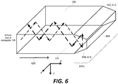
- FIG. 6 is a perspective view of a portion of a waveguide 100 that has a peripheral side 109d including a surface 602 that is planar and coextensive with a first plane 612, a surface 604 that is planar and coextensive with a second plane 614, and a surface 606 that extends between the surfaces 602 and 604, wherein the first and second planes 612 and 614 are 45 degrees relative to one another.
- the waveguide 100 includes an input-coupler 112 and an output-coupler 116, and may also include an intermediate-component 114, each of which function in the manners described above with reference to FIGS. 1A, 1B, 1C and 2 .
- the light that is recycled by the peripheral side 109d will travel in the direction opposite a propagation direction 620 at an angle relative to the y-z plane that is reversed in sign (compared to the light that travelled in the propagation direction 620).
- the sign of the angle of the recycled light in the orthogonal plane would be reversed.
- the x component of light traveling in the propagation direction 620 were plus 7 degrees, then the x component of the recycled light would be minus 7 degrees, which may cause undesirable ghost images.
- the surfaces 602 and 604 are coated with a reflective coating, examples of which were described above with reference to the reflective coating 302 described with reference to FIGS. 3 and 4 .
- the waveguide 100 can be designed such that substantially all of the light (after traveling within the waveguide) that is incident on the peripheral side 109d will experience TIR, then the surfaces 602 and 604 need not be coated with a reflective coating.
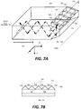
- FIG. 7A is a perspective view of a portion of a waveguide 100 that has a peripheral side 109d including a multifaceted surface 702 and a planar surface 704.
- FIG. 7B is a cross-section view of the waveguide 100 shown in FIG. 7A , along the line B-B in FIG. 7A .
- the waveguide 100 includes an input-coupler 112 and an output-coupler 116, and may also include an intermediate-component 114, each of which function in the manners described above with reference to FIGS. 1A, 1B, 1C and 2 .
- the multifaceted surface 702 includes a plurality of peaks 707 that collectively define a first plane 712.
- the planar surface 704 is coextensive with and thereby defines a second plane 714.
- the first and second planes 712 and 714 are 45 degrees relative to one another.
- Each of the peaks 707 of the multifaceted surface 702 is formed by a pair of adjacent facets 703 that are 90 degrees relative to one another.
- the multifaceted surface 702 also includes a plurality of valleys 709 each of which is formed by a pair of adjacent facets 703 that are 90 degrees relative to one another.
- the x component of the recycled light would also be plus 7 degrees. More specifically, when light is incident on one of the facets 703 of the multifaceted surface 702, that light will be directed toward an adjacent one of the facets 703 (wherein the two facets are 90 degrees relative to one another and meet for form a peak 707) before being reflected away from the multifaceted surface 702. This is what preserves the sign of the angle of the recycled light in the orthogonal plane (the x-y plane in this example).
- the surfaces 702 and 704 are coated with a reflective coating, examples of which were described above with reference to the reflective coating 302 described with reference to FIGS. 3 and 4 .
- the waveguide 100 can be designed such that substantially all of the light (while traveling within the waveguide) that is incident on the peripheral side 109d will experience TIR, then the surfaces 702 and 704 need not be coated with a reflective coating.
- the surface 702 was shown as being multifaceted and the surface 704 was shown as being planar.
- the surface 702 can be planar and the surface 704 can be multifaceted, and the peripheral side 109d would similarly effectively recycle light in a manner that maintains the sign of the angle of the recycled light in the orthogonal plane (the x-y plane in this example).
- peripheral side geometries shown in and described with reference to FIGS. 5 , 6 , 7A and 7B decouple alignment errors between the major sides 108 and 110 and the peripheral side 109d. It is relatively easy to manufacture a waveguide 100 having first and second major sides 108 and 110 that are parallel to one another. It is also relative easy to manufacture a peripheral side 109 having a pair of surfaces (e.g., 502 and 504, 602 and 604, or 702 and 704) that define first and second planes (e.g., 512 and 514, or 612 and 614, or 712 and 714) that are angled 45 degrees relative to one another.
- first and second planes e.g., 512 and 514, or 612 and 614, or 712 and 714
- peripheral side 109 that is precisely 90 degrees relative to the first and second major sides 108 and 110, which makes adding a reflective coating to a completely planar peripheral side 109 impractical.
- the embodiments of the present technology that were described above with reference to FIGS. 7A and 7B overcome this problem by utilizing a peripheral side geometry that is not sensitive to alignment relative to the major sides 108 and 110 of the waveguide 100.
- a peripheral side 109 includes a pair of surfaces (e.g., 502 and 504, 602 and 604, or 702 and 704) that define first and second planes (e.g., 512 and 514, or 612 and 614, or 712 and 714) that are angled 45 degrees relative to one another, the angles of portions of the peripheral side 109 relative to the major sides 108 and 110 are not critical.
- first and second planes e.g., 512 and 514, or 612 and 614, or 712 and 714
- a peripheral side 109 that includes a pair of surfaces (e.g., 502 and 504, 602 and 604, or 702 and 704) that define first and second planes (e.g., 512 and 514, or 612 and 614, or 712 and 714) that are angled 45 degrees relative to one another.
- first and second planes e.g., 512 and 514, or 612 and 614, or 712 and 714.
- one or more high precision bevel tools can be used to create the chamfered or bevelled geometries described herein.
- a waveguide with one or more peripheral sides having one of the desired geometries described herein can be produced using a mold. The use of other manufacturing techniques are also possible and within the scope of the embodiments of the present technology.
- the peripheral side 109d was described as having the geometry where a pair of surfaces (e.g., 502 and 504, 602 and 604, or 702 and 704) that define first and second planes (e.g., 512 and 514, or 612 and 614, or 712 and 714) are angled 45 degrees relative to one another.
- a pair of surfaces e.g., 502 and 504, 602 and 604, or 702 and 704
- first and second planes e.g., 512 and 514, or 612 and 614, or 712 and 71
- one or more of the other peripheral sides (e.g., 109a, 109b and/or 109c) of an optical waveguide 100 may have the same geometry that provides for effective recycling of light that while traveling within the waveguide is incident thereon. Utilizing this peripheral side geometry on additional peripheral sides 109 should further increase the optical efficiency of the waveguide.
- the optical efficiency of a waveguide refers to the amount of light that is coupled into the waveguide through an input-coupler of the waveguide divided by the amount of light that is coupled out of the waveguide through an output-coupler of the waveguide.
- a peripheral side 109 having a pair of surfaces that define first and second planes that are 45 degrees relative to one another an alternative option would be manufacture a peripheral side 109 having a pair of planar surfaces that are 90 degrees relative to one another.
- the planar surfaces 602 and 604 instead of having the planar surfaces 602 and 604 (of the peripheral side 109d) be 45 degrees relative to one another, the planar surfaces 602 and 604 can instead be 90 degrees relative to one another, and the side 606 can be eliminated so that the planar surfaces meet at a 90 degree angle.
- Such an alternative is believed to be inferior to the embodiments of the present technology described herein (where a peripheral side includes first and second surfaces that define first and second planes angled 45 degrees relative to one another).
- the 45 degree arrangement allows for a larger aperture for recycling light without causing ghost images than the 90 degree arrangement. Additionally, the 90 degree arrangement will only recycle light rays without causing ghost images if the light rays are incident on a surface of the peripheral side after traveling within the waveguide by way of TIR at an angle (relative to the normal to the major sides of the waveguide) that is greater than 45 degrees. This is because such light rays would only reflect off one of the two surfaces (of the peripheral side) that are at 90 degrees relative to one another.
- the 45 degree arrangement will recycle light rays without causing ghost images even where the light rays are incident on a surface of the peripheral side after traveling within the waveguide by way of TIR at an angle (relative to the normal to the major sides of the waveguide) that is less than 45 degrees.
- each of the optical waveguides described herein can be for use with a display engine, which can be the same as or similar to the display engine 204 described above with reference to FIG. 2 , but is not limited thereto.
- the display engine e.g., 204
- a user's eye e.g., the eye of a person wearing HMD glasses
- the input-coupler and the output-coupler can be implemented in a manner such that the display engine and a user's eye are proximate to and face a same major side of the optical waveguide.
- the optical waveguides described herein can be incorporated into a see-through mixed reality display device system.
- the same waveguide can be used to steer light of multiple different colors (e.g., red, green and blue) associated with an image from the input-coupler to the output-coupler.
- three waveguides can be stacked adjacent to each other, with each of the waveguides being used to steer light of a different colors (e.g., red, green or blue) associated with an image from its respective input-coupler to its output-coupler.
- a different colors e.g., red, green or blue
- one waveguide handle light of two colors (e.g., green and blue) and another waveguide handles light of a third color (e.g., red).
- Other variations are also possible.
- FIG. 8 is a high level flow diagram that is used to summarize methods according to certain embodiments of the present technology.
- Such methods which can be for use with a near-eye or heads-up display system including an optical waveguide, can use the optical waveguide to replicate an image associated with an input-pupil to an output-pupil.
- Such an optical waveguide includes at least an input-coupler and an output-coupler, and may also include an intermediate-component
- step 802 involves producing light corresponding to an image
- step 804 involves coupling the light corresponding to the image into an optical waveguide. More specifically, step 804 can involve coupling light corresponding to an image associated with an input-pupil into a bulk-substrate of an optical waveguide.
- step 802 is performed using a display engine, which can be the same as or similar to the display engine 204 described above with reference to FIG. 2 , but is not limited thereto.
- the coupling of the light corresponding to the image into optical waveguide at step 804 is performed using an input-coupler (e.g., 112) of the optical waveguide (e.g. 100).
- step 806 involves coupling out of the bulk-substrate of the optical waveguide, light corresponding to the image that has traveled through the optical waveguide from the input-coupler to the output-coupler at least in part by way of total internal reflection (TIR).
- step 804 is performed using an output-coupler (e.g., 116) of the optical waveguide (e.g., 100).
- Step 808 involves recycling at least a portion (and preferably all) of the light corresponding to the image, that is incident on one of the peripheral sides that includes first and second surfaces that define first and second planes angled 45 degrees relative to one another (after the portion of the light corresponding to the image has traveled within the bulk-substrate of the optical waveguide in a propagation direction toward the one of the peripheral sides).
- the recycling of light that is performed at step 808 is performed using the first and second surfaces that define the first and second planes angled 45 degrees relative to one another. Exemplary details of such surfaces and planes were described above with reference to FIGS. 5 , 6 , 7A and 7B . For example, referring back to FIG.
- step 808 can involve using one of the surfaces 502 or 504 to reflect, towards the other one of the surfaces 502 or 504, a portion of the light corresponding to an image that after being coupled into the waveguide 100 is incident on one of the surfaces 502 or 504.
- Such light may be incident on one of the surfaces 502 or 504 after traveling within the bulk-substrate 106 of the optical waveguide 100 at an angle of incidence relative to first and second major sides 108 and 110 in a propagation direction 520 toward the peripheral side 109d.
- Step 808 can also involve using the other one of the surfaces 502 or 504 to reflect the portion of the light corresponding to the image incident therein in a direction opposite the propagation direction 520 with the same angle of incidence relative to the first and second major sides 108 and 110.
- both of the surfaces can be planar surfaces that are coextensive with and define first and second planes (e.g., 512 and 514, or 612 and 614).
- first and second planes e.g., 512 and 514, or 612 and 614.
- one of the surfaces e.g., 502 or 702
- the other one of the surfaces can be and a planar surface (e.g., 504 or 704).
- Such a multifaceted surface includes a plurality of peaks and a plurality of valleys, with each of the peaks formed by a pair of adjacent facets of the multifaceted surface that are 90 degrees relative to one another, and each of the valleys similarly formed by a pair of adjacent facets of the multifaceted surface that are 90 degrees relative to one another.
- the peaks of the multifaceted surface collectively define one of the first and second planes, and the other one of the first and second surfaces is planar and defines the other one of the first and second planes.
- Use of the multifaceted surface preserves a sign, of the portion of the light corresponding to the image that is reflected in the direction opposite the propagation direction after being incident on the peripheral sides, in an orthogonal plane relative to the first and second major sides (e.g., 108 and 110) of the optical waveguide.
- the methods described with reference to FIG. 8 can be performed using an optical waveguide that includes at least an input-coupler and an output-coupler, and may also include an intermediate-component.
- the optical waveguide includes an input-coupler (e.g., 112) and an output-coupler (e.g., 116), but not an intermediate-component (e.g., 114)
- the input-coupler will direct light that it couples into the optical waveguide toward the output-coupler, and the output-coupler may provide one of horizontal or vertical pupil expansion.
- the input-coupler can be used to direct the light corresponding to the image (that is coupled into the bulk-substrate of the optical waveguide) toward the intermediate-component.
- the intermediate-component can be used to perform one of horizontal or vertical pupil expansion and to direct the light corresponding to the image towards the output-coupler, and the output-coupler can be used to perform the other one of horizontal or vertical pupil expansion. Additional details of the methods summarized with reference to FIG. 8 can be appreciated from the above discussion of FIGS. 1A, 1B, 1C , 2-6 , 7A and 7B .
Landscapes
- Physics & Mathematics (AREA)
- General Physics & Mathematics (AREA)
- Optics & Photonics (AREA)
- Optical Couplings Of Light Guides (AREA)
Claims (11)
- Einrichtung zur Verwendung beim Replizieren eines Bildes, das mit einer Eintrittspupille zusammenhängt, auf eine Austrittspupille, wobei die Einrichtung umfasst:einen optischen Wellenleiter (100), der ein Bulk-Substrat (106), einen Einkoppler (112) und einen Auskoppler (116) einschließt;wobei das Bulk-Substrat (106) des optischen Wellenleiters (100) eine erste Hauptseite (108), eine zweite Hauptseite (110) gegenüber der ersten Hauptseite (108), und Randseiten (109) einschließt;wobei der Einkoppler (112) des optischen Wellenleiters (100) so ausgelegt ist, dass er Licht, das dem mit der Eintrittspupille zusammenhängenden Bild entspricht, in das Bulk-Substrat (106) des optischen Wellenleiters (100) einkoppelt; undwobei der Auskoppler (116) des optischen Wellenleiters (100) so ausgelegt ist, dass er dem Bild entsprechendes Licht, das den optischen Wellenleiter (100) mindestens zum Teil durch innere Totalreflexion (TIR) vom Einkoppler (112) zum Auskoppler (116) durchlaufen hat, aus dem Bulk-Substrat (106) des optischen Wellenleiters (100) auskoppelt;wobei eine oder mehrere der Randseiten (109) des Bulk-Substrats (106) des optischen Wellenleiters (100) eine erste und eine zweite Fläche (502 und 504, 602 und 604, 702 und 704) einschließen, die eine erste und eine zweite Ebene (512 und 514, 612 und 614, 712 und 714) definieren, die relativ zueinander um 45 Grad abgewinkelt sind, wobei die erste Fläche (502, 602, 702) eine erste gefaste oder abgeschrägte Kante definiert, die sich zwischen der Randseite (109) und der ersten Hauptseite (108) befindet; und die zweite Fläche (504, 604, 704) eine zweite gefaste oder abgeschrägte Kante definiert, die sich zwischen der Randseite (109) und der zweiten Hauptseite (110) befindet,wobei der Auskoppler so ausgelegt ist, dass er einen Teil des dem Bild entsprechenden Lichts, das auf eine der Randseiten (109) fällt, die eine erste und eine zweite Fläche einschließt, aus dem Auskoppler heraus ablenkt,wobei bei mindestens einer Randseite (109), die eine erste und eine zweite Fläche (702 und 704) einschließt, die eine erste und eine zweite Ebene (712 und 714) definieren, die relativ zueinander um 45 Grad abgewinkelt sind:die erste Fläche (702) eine mehrfacettige Fläche umfasst, die eine Vielzahl von Spitzen (707) und eine Vielzahl von Tälern (709) einschließt;jede der Spitzen (707) von einem Paar aneinandergrenzender Facetten (703) der mehrfacettigen Fläche gebildet wird, die 90 Grad relativ zueinander stehen;jedes der Täler (709) von einem Paar aneinandergrenzender Facetten (703) der mehrfacettigen Fläche gebildet wird, die 90 Grad relativ zueinander stehen;die Spitzen (709) zusammen die erste Ebene (712) definieren; unddie zweite Fläche (704) plan ist und die zweite Ebene (714) definiert.
- Einrichtung nach Anspruch 1, wobei jede Randseite (109), die eine erste und eine zweite Fläche (502 und 504, 602 und 604, 702 und 704) einschließt, die eine erste und eine zweite Ebene (512 und 514, 612 und 614, 712 und 714) definieren, die relativ zueinander um 45 Grad abgewinkelt sind, so ausgelegt ist, dass sie einen Teil des dem Bild entsprechenden Lichts, das auf die Randseite (109) fällt, nachdem es das Bulk-Substrat (106) des optischen Wellenleiters (100) in einer Ausbreitungsrichtung zur Randseite (109) hin durchlaufen hat, wiederverwertet.
- Einrichtung nach Anspruch 1, wobei jede Randseite (109), die eine erste und eine zweite Fläche (502 und 504, 602 und 604, 702 und 704) einschließt, die eine erste und eine zweite Ebene (512 und 514, 612 und 614, 712 und 714) definieren, die relativ zueinander um 45 Grad abgewinkelt sind, so ausgelegt ist, dass sie bewirkt, dass ein Teil des dem Bild entsprechenden Lichts, das, nachdem es in den Wellenleiter (100) eingekoppelt wurde, in einem Einfallswinkel relativ zur ersten und der zweiten Hauptseite (108 und 110) in einer Ausbreitungsrichtung zur Randseite (109) hin auf eine aus der ersten und der zweiten Fläche (502 und 504, 602 und 604, 702 und 704) fällt, nachdem es das Bulk-Substrat (106) des optischen Wellenleiters (100) durchlaufen hat, zu der anderen aus der ersten und der zweiten Fläche (502 und 504, 602 und 604, 702 und 704) der Randseite (109) hin reflektiert wird, und dann von der anderen aus der ersten und der zweiten Fläche (502 und 504, 602 und 604, 702 und 704) mit einem gleichen Einfallswinkel relativ zur ersten und der zweiten Hauptseite (108 und 110) in eine der Ausbreitungsrichtung entgegengesetzte Richtung reflektiert wird.
- Einrichtung nach einem der Ansprüche 1-3, wobei bei mindestens einer Randseite (109), die eine erste und eine zweite Fläche (502 und 504, 602 und 604, 702 und 704) einschließt, die eine erste und eine zweite Ebene (512 und 514, 612 und 614, 712 und 714) definieren, die relativ zueinander um 45 Grad abgewinkelt sind, die erste und die zweite Fläche (502 und 504, 602 und 604, 702 und 704) mit einem reflektierenden Material beschichtet sind.
- Einrichtung nach einem der Ansprüche 1-3, wobei bei mindestens einer Randseite (109), die eine erste und eine zweite Fläche (502 und 504, 602 und 604) einschließt, die eine erste und eine zweite Ebene (512 und 514, 612 und 614) definieren, die relativ zueinander um 45 Grad abgewinkelt sind, die erste und die zweite Fläche (502 und 504, 602 und 604) je plan sind, und die plane erste und zweite Fläche (502 und 504, 602 und 604) jeweils die erste und die zweite Ebene (512 und 514, 612 und 614) definieren, die 45 Grad relativ zueinander stehen.
- Einrichtung nach einem der Ansprüche 1-3, wobei bei mindestens einer Randseite (109), die eine erste und eine zweite Fläche (502 und 504, 602 und 604, 702 und 704) einschließt, die eine erste und eine zweite Ebene (512 und 514, 612 und 614, 712 und 714) definieren, die relativ zueinander um 45 Grad abgewinkelt sind:
die Randseite (109) ebenfalls eine dritte Fläche (506, 606, 706) einschließt, die sich zwischen der ersten und der zweiten Fläche (502 und 504, 602 und 604, 702 und 704) erstreckt. - Einrichtung nach einem der Ansprüche 1-3, wobei:der optische Wellenleiter (100) ebenfalls eine Zwischenkomponente (114) einschließt;der Einkoppler (112) so ausgelegt ist, dass er das Licht, das dem mit der Eintrittspupille zusammenhängenden Bild entspricht, das in das Bulk-Substrat (106) des Wellenleiters (100) eingekoppelt wird, zur Zwischenkomponente (114) hin lenkt;die Zwischenkomponente (114) so ausgelegt ist, dass sie eines aus horizontaler oder vertikaler Pupillenerweiterung durchführt und das dem Bild entsprechende Licht zum Auskoppler (116) hin lenkt; undder Auskoppler (116) so ausgelegt ist, dass er das andere aus horizontaler oder vertikaler Pupillenerweiterung durchführt.
- Verfahren zur Verwendung in einem optischen Wellenleiter (100), der ein Bulk-Substrat (106), einen Einkoppler (112) und einen Auskoppler (116) einschließt, wobei das Bulk-Substrat (106) des optischen Wellenleiters eine erste Hauptseite (108), eine zweite Hauptseite (110) gegenüber der ersten Hauptseite (108), und Randseiten (109) einschließt, wobei das Verfahren umfasst:Einkoppeln (804) von Licht, das einem mit einer Eintrittspupille zusammenhängenden Bild entspricht, unter Verwendung des Einkopplers (112) des optischen Wellenleiters (100) in das Bulk-Substrat (106) des optischen Wellenleiters (100);Auskoppeln (806) von dem Bild entsprechendem Licht, das den optischen Wellenleiter (100) mindestens zum Teil durch innere Totalreflexion (TIR) vom Einkoppler (112) zum Auskoppler (116) durchlaufen hat, unter Verwendung des Auskopplers (116) aus dem Bulk-Substrat (106) des optischen Wellenleiters (100); undWiederverwerten (808) eines Teils des dem Bild entsprechenden Lichts, das auf eine der Randseiten (109) fällt, die eine erste und eine zweite Fläche (502 und 504, 602 und 604, 702 und 704) einschließen, die eine erste und eine zweite Ebene (512 und 514, 612 und 614, 712 und 714) definieren, die relativ zueinander um 45 Grad abgewinkelt sind, nachdem der Teil des dem Bild entsprechenden Lichts das Bulk-Substrat (106) des optischen Wellenleiters (100) in einer Ausbreitungsrichtung zu der einen der Randseiten (109) hin durchlaufen hat, wobei das Wiederverwerten unter Verwendung der ersten und der zweiten Fläche (502 und 504, 602 und 604, 702 und 704), die eine erste und eine zweite Ebene (512 und 514, 612 und 614, 712 und 714) definieren, die relativ zueinander um 45 Grad abgewinkelt sind, durchgeführt wird, wobei die erste Fläche (502, 602, 702) eine erste gefaste oder abgeschrägte Kante definiert, die sich zwischen der Randseite (109) und der ersten Hauptseite (108) befindet; und die zweite Fläche (504, 604, 704) eine zweite gefaste oder abgeschrägte Kante definiert, die sich zwischen der Randseite (109) und der zweiten Hauptseite (110) befindet,wobei das wiederverwertete Licht aus dem Auskoppler heraus abgelenkt wird,wobei eine aus der ersten und der zweiten Fläche (702) der einen der Randseiten (109) eine mehrfacettige Fläche (702) umfasst, die eine Vielzahl von Spitzen (707) und eine Vielzahl von Tälern (709) einschließt, jede der Spitzen (707) von einem Paar aneinandergrenzender Facetten (703) der mehrfacettigen Fläche (702) gebildet wird, die 90 Grad relativ zueinander stehen, jedes der Täler (709) von einem Paar aneinandergrenzender Facetten (703) der mehrfacettigen Fläche (702) gebildet wird, die 90 Grad relativ zueinander stehen, die Spitzen (707) zusammen die eine aus der ersten und der zweiten Ebene (712) definieren, und die andere aus der ersten und der zweiten Fläche (704) plan ist und die andere aus der ersten und der zweiten Ebene (714) definiert; unddas Wiederverwerten das Verwenden der mehrfacettigen Fläche (702) einschließt, um ein Vorzeichen, in einer relativ zur ersten und der zweiten Hauptseite (108 und 110) orthogonalen Ebene, des Teils des dem Bild entsprechenden Lichts, das, nachdem es auf die eine der Randseiten (109) fällt, in der der Ausbreitungsrichtung entgegengesetzten Richtung reflektiert wird, beizubehalten.
- Verfahren nach Anspruch 8, wobei das Wiederverwerten einschließt:Verwenden einer aus der ersten und der zweiten Fläche (502 und 504, 602 und 604, 702 und 704), um einen Teil des dem Bild entsprechenden Lichts, das, nachdem es in den Wellenleiter eingekoppelt wurde, in einem Einfallswinkel relativ zur ersten und der zweiten Hauptseite in einer Ausbreitungsrichtung zu der einen der Randseiten hin auf die eine aus der ersten und der zweiten Fläche fällt, nachdem es das Bulk-Substrat des optischen Wellenleiters durchlaufen hat, zu der anderen aus der ersten und der zweiten Fläche (502 und 504, 602 und 604, 702 und 704) zu reflektieren; undVerwenden der anderen aus der ersten und der zweiten Fläche (502 und 504, 602 und 604, 702 und 704), um den Teil des dem Bild entsprechenden Lichts, das auf sie fällt, mit einem gleichen Einfallswinkel relativ zur ersten und der zweiten Hauptseite in eine der Ausbreitungsrichtung entgegengesetzte Richtung zu reflektieren.
- Verfahren nach Anspruch 8 oder 9, wobei die erste und die zweite Fläche (502 und 504, 602 und 604) der einen der Randseiten (109) je plan sind, und die plane erste und zweite Fläche (502 und 504, 602 und 604) jeweils die erste und die zweite Ebene (512 und 514, 612 und 614) definieren, die 45 Grad relativ zueinander stehen.
- Verfahren nach Anspruch 8 oder 9, wobei der optische Wellenleiter (100) ebenfalls eine Zwischenkomponente (114) einschließt, und weiter umfassend:Verwenden des Einkopplers (112), um das dem Bild entsprechende Licht, das in das Bulk-Substrat (106) des optischen Wellenleiters (100) eingekoppelt wird, zur Zwischenkomponente (114) hin zu lenken; undVerwenden der Zwischenkomponente (114), um eines aus horizontaler oder vertikaler Pupillenerweiterung durchzuführen und das dem Bild entsprechende Licht zum Auskoppler (116) hin zu lenken; undVerwenden des Auskopplers (116), um das andere aus horizontaler oder vertikaler Pupillenerweiterung durchzuführen.
Applications Claiming Priority (2)
| Application Number | Priority Date | Filing Date | Title |
|---|---|---|---|
| US15/370,897 US10310268B2 (en) | 2016-12-06 | 2016-12-06 | Waveguides with peripheral side geometries to recycle light |
| PCT/US2017/064102 WO2018106515A1 (en) | 2016-12-06 | 2017-12-01 | Waveguides with peripheral side geometries to recycle light |
Publications (2)
| Publication Number | Publication Date |
|---|---|
| EP3551931A1 EP3551931A1 (de) | 2019-10-16 |
| EP3551931B1 true EP3551931B1 (de) | 2021-07-28 |
Family
ID=60991498
Family Applications (1)
| Application Number | Title | Priority Date | Filing Date |
|---|---|---|---|
| EP17829739.6A Active EP3551931B1 (de) | 2016-12-06 | 2017-12-01 | Wellenleiter mit peripheren seitengeometrien zum recyceln von licht |
Country Status (4)
| Country | Link |
|---|---|
| US (1) | US10310268B2 (de) |
| EP (1) | EP3551931B1 (de) |
| CN (1) | CN110036235B (de) |
| WO (1) | WO2018106515A1 (de) |
Families Citing this family (9)
| Publication number | Priority date | Publication date | Assignee | Title |
|---|---|---|---|---|
| US10761256B2 (en) * | 2018-04-16 | 2020-09-01 | Samsung Electronics Co., Ltd. | Backlight unit providing uniform light and display apparatus including the same |
| JP7235850B2 (ja) * | 2018-08-13 | 2023-03-08 | レイア、インコーポレイテッド | 光リサイクル光源を用いるグレーティングコリメータ、バックライトシステム、及び方法 |
| GB201905773D0 (en) | 2019-04-25 | 2019-06-05 | Wave Optics Ltd | Display for augmented reality |
| EP3733139A1 (de) * | 2019-05-02 | 2020-11-04 | Gensight Biologics | Betrachtungsvorrichtung und verfahren zur projizierung eines lichtsignals |
| CN112444969B (zh) * | 2019-08-30 | 2022-10-18 | 成都理想境界科技有限公司 | 一种大视场双层深度ar波导 |
| CN114616506B (zh) * | 2019-11-01 | 2024-02-23 | 株式会社籁天那 | 具有重影阻挡功能和广视角的紧凑型增强现实用光学装置 |
| US20240103270A1 (en) * | 2019-11-06 | 2024-03-28 | Google Llc | Optical combiners with improved efficiency and uniformity |
| CN113325505A (zh) * | 2020-02-28 | 2021-08-31 | 苏州苏大维格科技集团股份有限公司 | 一种光波导镜片及三维显示装置 |
| TWI839769B (zh) * | 2022-07-05 | 2024-04-21 | 友達光電股份有限公司 | 抬頭顯示器及其操作方法 |
Family Cites Families (24)
| Publication number | Priority date | Publication date | Assignee | Title |
|---|---|---|---|---|
| US5303085A (en) | 1992-02-07 | 1994-04-12 | Rallison Richard D | Optically corrected helmet mounted display |
| US6144439A (en) | 1997-07-29 | 2000-11-07 | Kaiser Electro-Optics, Inc. | Method and apparatus for reducing ghost images with a tilted cholesteric liquid crystal panel |
| US5943171A (en) | 1998-06-03 | 1999-08-24 | International Business Machines Corporation | Head mounted displays utilizing reflection light valves |
| US6563992B1 (en) | 1998-07-02 | 2003-05-13 | Axiom Analytical, Inc. | Small diameter diffuse reflectance probe |
| US6785447B2 (en) | 1998-10-09 | 2004-08-31 | Fujitsu Limited | Single and multilayer waveguides and fabrication process |
| US20050174641A1 (en) | 2002-11-26 | 2005-08-11 | Jds Uniphase Corporation | Polarization conversion light integrator |
| JP4397394B2 (ja) | 2003-01-24 | 2010-01-13 | ディジタル・オプティクス・インターナショナル・コーポレイション | 高密度照明システム |
| GB0425215D0 (en) | 2004-11-16 | 2004-12-15 | Cambridge Flat Projection | Flat projection diffuser |
| DE102006033703A1 (de) | 2006-07-20 | 2008-01-24 | Kathrein-Werke Kg | Hohlleiterkrümmer |
| JP4450058B2 (ja) * | 2007-11-29 | 2010-04-14 | ソニー株式会社 | 画像表示装置 |
| EP2196729A1 (de) * | 2008-12-12 | 2010-06-16 | BAE Systems PLC | Verbesserungen an oder im Zusammenhang mit Wellenleitern |
| JP5278412B2 (ja) | 2010-11-17 | 2013-09-04 | オムロン株式会社 | 面光源装置及び立体表示装置 |
| JP5633406B2 (ja) | 2011-02-04 | 2014-12-03 | セイコーエプソン株式会社 | 虚像表示装置 |
| JP5720290B2 (ja) * | 2011-02-16 | 2015-05-20 | セイコーエプソン株式会社 | 虚像表示装置 |
| US8472119B1 (en) | 2011-08-12 | 2013-06-25 | Google Inc. | Image waveguide having a bend |
| CN104040410B (zh) * | 2011-08-29 | 2017-06-09 | 伊奎蒂公司 | 用于近眼显示器应用的可控波导 |
| US9459392B2 (en) | 2012-05-16 | 2016-10-04 | 3M Innovative Properties Company | Illumination converter |
| JP6510160B2 (ja) | 2012-10-22 | 2019-05-08 | セイコーエプソン株式会社 | 光学デバイス及び画像表示装置 |
| CN102998799A (zh) * | 2012-12-04 | 2013-03-27 | 深圳市长江力伟股份有限公司 | 一种虚境与实境融合近眼显示系统 |
| US9069115B2 (en) | 2013-04-25 | 2015-06-30 | Google Inc. | Edge configurations for reducing artifacts in eyepieces |
| CN107219628B (zh) | 2013-11-27 | 2020-05-01 | 奇跃公司 | 虚拟和增强现实系统与方法 |
| WO2015117023A1 (en) | 2014-01-31 | 2015-08-06 | Mack Corey | Augmented reality eyewear and methods for using same |
| RU2594370C2 (ru) | 2014-07-11 | 2016-08-20 | Самсунг Электроникс Ко., Лтд. | Световодная структура, оптическое устройство и система формирования изображений |
| CN105929545B (zh) * | 2016-06-20 | 2019-03-26 | 东莞市长资实业有限公司 | 波导式的头戴显示器的光学装置 |
-
2016
- 2016-12-06 US US15/370,897 patent/US10310268B2/en active Active
-
2017
- 2017-12-01 CN CN201780075177.XA patent/CN110036235B/zh active Active
- 2017-12-01 WO PCT/US2017/064102 patent/WO2018106515A1/en not_active Ceased
- 2017-12-01 EP EP17829739.6A patent/EP3551931B1/de active Active
Also Published As
| Publication number | Publication date |
|---|---|
| US20180157042A1 (en) | 2018-06-07 |
| CN110036235B (zh) | 2020-11-03 |
| US10310268B2 (en) | 2019-06-04 |
| EP3551931A1 (de) | 2019-10-16 |
| CN110036235A (zh) | 2019-07-19 |
| WO2018106515A1 (en) | 2018-06-14 |
Similar Documents
| Publication | Publication Date | Title |
|---|---|---|
| EP3551931B1 (de) | Wellenleiter mit peripheren seitengeometrien zum recyceln von licht | |
| EP3443402B1 (de) | Wellenleiter mit erweitertem gesichtsfeld | |
| US10353202B2 (en) | Wrapped waveguide with large field of view | |
| US10551616B2 (en) | Display device system with tilted lens group to prevent ghost images | |
| EP3631561B1 (de) | Anzeigevorrichtungssystem mit nichttelezentrischer bildgebung zur verhinderung von geisterbildern | |
| US12130443B2 (en) | Waveguide for transmitting light | |
| US9891436B2 (en) | Waveguide-based displays with anti-reflective and highly-reflective coating | |
| US9989763B2 (en) | Imaging using multiple different narrow bands of light having respective different emission peaks | |
| US20170299860A1 (en) | Waveguide-Based Displays With Exit Pupil Expander | |
| CN219349182U (zh) | 一种光波导和近眼显示装置 | |
| EP4224238B1 (de) | Multipupillen-erweiterungslichtleiteranordnung mit stange | |
| US20250321425A1 (en) | Waveguide stack architecture with high red efficiency |
Legal Events
| Date | Code | Title | Description |
|---|---|---|---|
| STAA | Information on the status of an ep patent application or granted ep patent |
Free format text: STATUS: UNKNOWN |
|
| STAA | Information on the status of an ep patent application or granted ep patent |
Free format text: STATUS: THE INTERNATIONAL PUBLICATION HAS BEEN MADE |
|
| PUAI | Public reference made under article 153(3) epc to a published international application that has entered the european phase |
Free format text: ORIGINAL CODE: 0009012 |
|
| STAA | Information on the status of an ep patent application or granted ep patent |
Free format text: STATUS: REQUEST FOR EXAMINATION WAS MADE |
|
| 17P | Request for examination filed |
Effective date: 20190515 |
|
| AK | Designated contracting states |
Kind code of ref document: A1 Designated state(s): AL AT BE BG CH CY CZ DE DK EE ES FI FR GB GR HR HU IE IS IT LI LT LU LV MC MK MT NL NO PL PT RO RS SE SI SK SM TR |
|
| AX | Request for extension of the european patent |
Extension state: BA ME |
|
| DAV | Request for validation of the european patent (deleted) | ||
| DAX | Request for extension of the european patent (deleted) | ||
| GRAP | Despatch of communication of intention to grant a patent |
Free format text: ORIGINAL CODE: EPIDOSNIGR1 |
|
| STAA | Information on the status of an ep patent application or granted ep patent |
Free format text: STATUS: GRANT OF PATENT IS INTENDED |
|
| INTG | Intention to grant announced |
Effective date: 20210208 |
|
| GRAJ | Information related to disapproval of communication of intention to grant by the applicant or resumption of examination proceedings by the epo deleted |
Free format text: ORIGINAL CODE: EPIDOSDIGR1 |
|
| STAA | Information on the status of an ep patent application or granted ep patent |
Free format text: STATUS: REQUEST FOR EXAMINATION WAS MADE |
|
| GRAP | Despatch of communication of intention to grant a patent |
Free format text: ORIGINAL CODE: EPIDOSNIGR1 |
|
| STAA | Information on the status of an ep patent application or granted ep patent |
Free format text: STATUS: GRANT OF PATENT IS INTENDED |
|
| INTC | Intention to grant announced (deleted) | ||
| GRAS | Grant fee paid |
Free format text: ORIGINAL CODE: EPIDOSNIGR3 |
|
| GRAA | (expected) grant |
Free format text: ORIGINAL CODE: 0009210 |
|
| STAA | Information on the status of an ep patent application or granted ep patent |
Free format text: STATUS: THE PATENT HAS BEEN GRANTED |
|
| INTG | Intention to grant announced |
Effective date: 20210609 |
|
| AK | Designated contracting states |
Kind code of ref document: B1 Designated state(s): AL AT BE BG CH CY CZ DE DK EE ES FI FR GB GR HR HU IE IS IT LI LT LU LV MC MK MT NL NO PL PT RO RS SE SI SK SM TR |
|
| REG | Reference to a national code |
Ref country code: GB Ref legal event code: FG4D |
|
| REG | Reference to a national code |
Ref country code: CH Ref legal event code: EP |
|
| REG | Reference to a national code |
Ref country code: DE Ref legal event code: R096 Ref document number: 602017043069 Country of ref document: DE |
|
| REG | Reference to a national code |
Ref country code: AT Ref legal event code: REF Ref document number: 1415029 Country of ref document: AT Kind code of ref document: T Effective date: 20210815 |
|
| REG | Reference to a national code |
Ref country code: IE Ref legal event code: FG4D |
|
| REG | Reference to a national code |
Ref country code: NL Ref legal event code: FP |
|
| RAP4 | Party data changed (patent owner data changed or rights of a patent transferred) |
Owner name: MICROSOFT TECHNOLOGY LICENSING, LLC |
|
| REG | Reference to a national code |
Ref country code: LT Ref legal event code: MG9D |
|
| REG | Reference to a national code |
Ref country code: AT Ref legal event code: MK05 Ref document number: 1415029 Country of ref document: AT Kind code of ref document: T Effective date: 20210728 |
|
| PG25 | Lapsed in a contracting state [announced via postgrant information from national office to epo] |
Ref country code: BG Free format text: LAPSE BECAUSE OF FAILURE TO SUBMIT A TRANSLATION OF THE DESCRIPTION OR TO PAY THE FEE WITHIN THE PRESCRIBED TIME-LIMIT Effective date: 20211028 Ref country code: AT Free format text: LAPSE BECAUSE OF FAILURE TO SUBMIT A TRANSLATION OF THE DESCRIPTION OR TO PAY THE FEE WITHIN THE PRESCRIBED TIME-LIMIT Effective date: 20210728 Ref country code: LT Free format text: LAPSE BECAUSE OF FAILURE TO SUBMIT A TRANSLATION OF THE DESCRIPTION OR TO PAY THE FEE WITHIN THE PRESCRIBED TIME-LIMIT Effective date: 20210728 Ref country code: NO Free format text: LAPSE BECAUSE OF FAILURE TO SUBMIT A TRANSLATION OF THE DESCRIPTION OR TO PAY THE FEE WITHIN THE PRESCRIBED TIME-LIMIT Effective date: 20211028 Ref country code: PT Free format text: LAPSE BECAUSE OF FAILURE TO SUBMIT A TRANSLATION OF THE DESCRIPTION OR TO PAY THE FEE WITHIN THE PRESCRIBED TIME-LIMIT Effective date: 20211129 Ref country code: SE Free format text: LAPSE BECAUSE OF FAILURE TO SUBMIT A TRANSLATION OF THE DESCRIPTION OR TO PAY THE FEE WITHIN THE PRESCRIBED TIME-LIMIT Effective date: 20210728 Ref country code: RS Free format text: LAPSE BECAUSE OF FAILURE TO SUBMIT A TRANSLATION OF THE DESCRIPTION OR TO PAY THE FEE WITHIN THE PRESCRIBED TIME-LIMIT Effective date: 20210728 Ref country code: HR Free format text: LAPSE BECAUSE OF FAILURE TO SUBMIT A TRANSLATION OF THE DESCRIPTION OR TO PAY THE FEE WITHIN THE PRESCRIBED TIME-LIMIT Effective date: 20210728 Ref country code: ES Free format text: LAPSE BECAUSE OF FAILURE TO SUBMIT A TRANSLATION OF THE DESCRIPTION OR TO PAY THE FEE WITHIN THE PRESCRIBED TIME-LIMIT Effective date: 20210728 Ref country code: FI Free format text: LAPSE BECAUSE OF FAILURE TO SUBMIT A TRANSLATION OF THE DESCRIPTION OR TO PAY THE FEE WITHIN THE PRESCRIBED TIME-LIMIT Effective date: 20210728 |
|
| PG25 | Lapsed in a contracting state [announced via postgrant information from national office to epo] |
Ref country code: PL Free format text: LAPSE BECAUSE OF FAILURE TO SUBMIT A TRANSLATION OF THE DESCRIPTION OR TO PAY THE FEE WITHIN THE PRESCRIBED TIME-LIMIT Effective date: 20210728 Ref country code: LV Free format text: LAPSE BECAUSE OF FAILURE TO SUBMIT A TRANSLATION OF THE DESCRIPTION OR TO PAY THE FEE WITHIN THE PRESCRIBED TIME-LIMIT Effective date: 20210728 Ref country code: GR Free format text: LAPSE BECAUSE OF FAILURE TO SUBMIT A TRANSLATION OF THE DESCRIPTION OR TO PAY THE FEE WITHIN THE PRESCRIBED TIME-LIMIT Effective date: 20211029 |
|
| PG25 | Lapsed in a contracting state [announced via postgrant information from national office to epo] |
Ref country code: DK Free format text: LAPSE BECAUSE OF FAILURE TO SUBMIT A TRANSLATION OF THE DESCRIPTION OR TO PAY THE FEE WITHIN THE PRESCRIBED TIME-LIMIT Effective date: 20210728 |
|
| REG | Reference to a national code |
Ref country code: DE Ref legal event code: R097 Ref document number: 602017043069 Country of ref document: DE |
|
| PG25 | Lapsed in a contracting state [announced via postgrant information from national office to epo] |
Ref country code: SM Free format text: LAPSE BECAUSE OF FAILURE TO SUBMIT A TRANSLATION OF THE DESCRIPTION OR TO PAY THE FEE WITHIN THE PRESCRIBED TIME-LIMIT Effective date: 20210728 Ref country code: SK Free format text: LAPSE BECAUSE OF FAILURE TO SUBMIT A TRANSLATION OF THE DESCRIPTION OR TO PAY THE FEE WITHIN THE PRESCRIBED TIME-LIMIT Effective date: 20210728 Ref country code: RO Free format text: LAPSE BECAUSE OF FAILURE TO SUBMIT A TRANSLATION OF THE DESCRIPTION OR TO PAY THE FEE WITHIN THE PRESCRIBED TIME-LIMIT Effective date: 20210728 Ref country code: EE Free format text: LAPSE BECAUSE OF FAILURE TO SUBMIT A TRANSLATION OF THE DESCRIPTION OR TO PAY THE FEE WITHIN THE PRESCRIBED TIME-LIMIT Effective date: 20210728 Ref country code: CZ Free format text: LAPSE BECAUSE OF FAILURE TO SUBMIT A TRANSLATION OF THE DESCRIPTION OR TO PAY THE FEE WITHIN THE PRESCRIBED TIME-LIMIT Effective date: 20210728 Ref country code: AL Free format text: LAPSE BECAUSE OF FAILURE TO SUBMIT A TRANSLATION OF THE DESCRIPTION OR TO PAY THE FEE WITHIN THE PRESCRIBED TIME-LIMIT Effective date: 20210728 |
|
| PLBE | No opposition filed within time limit |
Free format text: ORIGINAL CODE: 0009261 |
|
| STAA | Information on the status of an ep patent application or granted ep patent |
Free format text: STATUS: NO OPPOSITION FILED WITHIN TIME LIMIT |
|
| 26N | No opposition filed |
Effective date: 20220429 |
|
| PG25 | Lapsed in a contracting state [announced via postgrant information from national office to epo] |
Ref country code: MC Free format text: LAPSE BECAUSE OF FAILURE TO SUBMIT A TRANSLATION OF THE DESCRIPTION OR TO PAY THE FEE WITHIN THE PRESCRIBED TIME-LIMIT Effective date: 20210728 Ref country code: IT Free format text: LAPSE BECAUSE OF FAILURE TO SUBMIT A TRANSLATION OF THE DESCRIPTION OR TO PAY THE FEE WITHIN THE PRESCRIBED TIME-LIMIT Effective date: 20210728 |
|
| REG | Reference to a national code |
Ref country code: CH Ref legal event code: PL |
|
| REG | Reference to a national code |
Ref country code: BE Ref legal event code: MM Effective date: 20211231 |
|
| PG25 | Lapsed in a contracting state [announced via postgrant information from national office to epo] |
Ref country code: LU Free format text: LAPSE BECAUSE OF NON-PAYMENT OF DUE FEES Effective date: 20211201 Ref country code: IE Free format text: LAPSE BECAUSE OF NON-PAYMENT OF DUE FEES Effective date: 20211201 |
|
| PG25 | Lapsed in a contracting state [announced via postgrant information from national office to epo] |
Ref country code: BE Free format text: LAPSE BECAUSE OF NON-PAYMENT OF DUE FEES Effective date: 20211231 |
|
| PG25 | Lapsed in a contracting state [announced via postgrant information from national office to epo] |
Ref country code: LI Free format text: LAPSE BECAUSE OF NON-PAYMENT OF DUE FEES Effective date: 20211231 Ref country code: CH Free format text: LAPSE BECAUSE OF NON-PAYMENT OF DUE FEES Effective date: 20211231 |
|
| P01 | Opt-out of the competence of the unified patent court (upc) registered |
Effective date: 20230430 |
|
| PG25 | Lapsed in a contracting state [announced via postgrant information from national office to epo] |
Ref country code: CY Free format text: LAPSE BECAUSE OF FAILURE TO SUBMIT A TRANSLATION OF THE DESCRIPTION OR TO PAY THE FEE WITHIN THE PRESCRIBED TIME-LIMIT Effective date: 20210728 |
|
| PG25 | Lapsed in a contracting state [announced via postgrant information from national office to epo] |
Ref country code: HU Free format text: LAPSE BECAUSE OF FAILURE TO SUBMIT A TRANSLATION OF THE DESCRIPTION OR TO PAY THE FEE WITHIN THE PRESCRIBED TIME-LIMIT; INVALID AB INITIO Effective date: 20171201 |
|
| PG25 | Lapsed in a contracting state [announced via postgrant information from national office to epo] |
Ref country code: MK Free format text: LAPSE BECAUSE OF FAILURE TO SUBMIT A TRANSLATION OF THE DESCRIPTION OR TO PAY THE FEE WITHIN THE PRESCRIBED TIME-LIMIT Effective date: 20210728 |
|
| PG25 | Lapsed in a contracting state [announced via postgrant information from national office to epo] |
Ref country code: TR Free format text: LAPSE BECAUSE OF FAILURE TO SUBMIT A TRANSLATION OF THE DESCRIPTION OR TO PAY THE FEE WITHIN THE PRESCRIBED TIME-LIMIT Effective date: 20210728 |
|
| PG25 | Lapsed in a contracting state [announced via postgrant information from national office to epo] |
Ref country code: MT Free format text: LAPSE BECAUSE OF FAILURE TO SUBMIT A TRANSLATION OF THE DESCRIPTION OR TO PAY THE FEE WITHIN THE PRESCRIBED TIME-LIMIT Effective date: 20210728 |
|
| PGFP | Annual fee paid to national office [announced via postgrant information from national office to epo] |
Ref country code: NL Payment date: 20251119 Year of fee payment: 9 |
|
| PGFP | Annual fee paid to national office [announced via postgrant information from national office to epo] |
Ref country code: DE Payment date: 20251126 Year of fee payment: 9 |
|
| PGFP | Annual fee paid to national office [announced via postgrant information from national office to epo] |
Ref country code: GB Payment date: 20251119 Year of fee payment: 9 |
|
| PGFP | Annual fee paid to national office [announced via postgrant information from national office to epo] |
Ref country code: FR Payment date: 20251120 Year of fee payment: 9 |