EP3550628B1 - Display device, method of manufacturing the same, and glass stack - Google Patents
Display device, method of manufacturing the same, and glass stack Download PDFInfo
- Publication number
- EP3550628B1 EP3550628B1 EP19167021.5A EP19167021A EP3550628B1 EP 3550628 B1 EP3550628 B1 EP 3550628B1 EP 19167021 A EP19167021 A EP 19167021A EP 3550628 B1 EP3550628 B1 EP 3550628B1
- Authority
- EP
- European Patent Office
- Prior art keywords
- coating layer
- frit
- encapsulation substrate
- light emitting
- substrate
- Prior art date
- Legal status (The legal status is an assumption and is not a legal conclusion. Google has not performed a legal analysis and makes no representation as to the accuracy of the status listed.)
- Active
Links
Images











Classifications
-
- C—CHEMISTRY; METALLURGY
- C03—GLASS; MINERAL OR SLAG WOOL
- C03C—CHEMICAL COMPOSITION OF GLASSES, GLAZES OR VITREOUS ENAMELS; SURFACE TREATMENT OF GLASS; SURFACE TREATMENT OF FIBRES OR FILAMENTS MADE FROM GLASS, MINERALS OR SLAGS; JOINING GLASS TO GLASS OR OTHER MATERIALS
- C03C17/00—Surface treatment of glass, not in the form of fibres or filaments, by coating
- C03C17/28—Surface treatment of glass, not in the form of fibres or filaments, by coating with organic material
- C03C17/32—Surface treatment of glass, not in the form of fibres or filaments, by coating with organic material with synthetic or natural resins
-
- C—CHEMISTRY; METALLURGY
- C03—GLASS; MINERAL OR SLAG WOOL
- C03C—CHEMICAL COMPOSITION OF GLASSES, GLAZES OR VITREOUS ENAMELS; SURFACE TREATMENT OF GLASS; SURFACE TREATMENT OF FIBRES OR FILAMENTS MADE FROM GLASS, MINERALS OR SLAGS; JOINING GLASS TO GLASS OR OTHER MATERIALS
- C03C27/00—Joining pieces of glass to pieces of other inorganic material; Joining glass to glass other than by fusing
- C03C27/06—Joining glass to glass by processes other than fusing
- C03C27/10—Joining glass to glass by processes other than fusing with the aid of adhesive specially adapted for that purpose
-
- C—CHEMISTRY; METALLURGY
- C09—DYES; PAINTS; POLISHES; NATURAL RESINS; ADHESIVES; COMPOSITIONS NOT OTHERWISE PROVIDED FOR; APPLICATIONS OF MATERIALS NOT OTHERWISE PROVIDED FOR
- C09D—COATING COMPOSITIONS, e.g. PAINTS, VARNISHES OR LACQUERS; FILLING PASTES; CHEMICAL PAINT OR INK REMOVERS; INKS; CORRECTING FLUIDS; WOODSTAINS; PASTES OR SOLIDS FOR COLOURING OR PRINTING; USE OF MATERIALS THEREFOR
- C09D123/00—Coating compositions based on homopolymers or copolymers of unsaturated aliphatic hydrocarbons having only one carbon-to-carbon double bond; Coating compositions based on derivatives of such polymers
- C09D123/02—Coating compositions based on homopolymers or copolymers of unsaturated aliphatic hydrocarbons having only one carbon-to-carbon double bond; Coating compositions based on derivatives of such polymers not modified by chemical after-treatment
- C09D123/04—Homopolymers or copolymers of ethene
- C09D123/08—Copolymers of ethene
- C09D123/0846—Copolymers of ethene with unsaturated hydrocarbons containing other atoms than carbon or hydrogen atoms
-
- G—PHYSICS
- G02—OPTICS
- G02B—OPTICAL ELEMENTS, SYSTEMS OR APPARATUS
- G02B5/00—Optical elements other than lenses
- G02B5/30—Polarising elements
- G02B5/3025—Polarisers, i.e. arrangements capable of producing a definite output polarisation state from an unpolarised input state
-
- G—PHYSICS
- G06—COMPUTING OR CALCULATING; COUNTING
- G06F—ELECTRIC DIGITAL DATA PROCESSING
- G06F3/00—Input arrangements for transferring data to be processed into a form capable of being handled by the computer; Output arrangements for transferring data from processing unit to output unit, e.g. interface arrangements
- G06F3/01—Input arrangements or combined input and output arrangements for interaction between user and computer
- G06F3/03—Arrangements for converting the position or the displacement of a member into a coded form
- G06F3/041—Digitisers, e.g. for touch screens or touch pads, characterised by the transducing means
- G06F3/0412—Digitisers structurally integrated in a display
-
- G—PHYSICS
- G09—EDUCATION; CRYPTOGRAPHY; DISPLAY; ADVERTISING; SEALS
- G09G—ARRANGEMENTS OR CIRCUITS FOR CONTROL OF INDICATING DEVICES USING STATIC MEANS TO PRESENT VARIABLE INFORMATION
- G09G3/00—Control arrangements or circuits, of interest only in connection with visual indicators other than cathode-ray tubes
- G09G3/20—Control arrangements or circuits, of interest only in connection with visual indicators other than cathode-ray tubes for presentation of an assembly of a number of characters, e.g. a page, by composing the assembly by combination of individual elements arranged in a matrix no fixed position being assigned to or needed to be assigned to the individual characters or partial characters
- G09G3/22—Control arrangements or circuits, of interest only in connection with visual indicators other than cathode-ray tubes for presentation of an assembly of a number of characters, e.g. a page, by composing the assembly by combination of individual elements arranged in a matrix no fixed position being assigned to or needed to be assigned to the individual characters or partial characters using controlled light sources
-
- H—ELECTRICITY
- H10—SEMICONDUCTOR DEVICES; ELECTRIC SOLID-STATE DEVICES NOT OTHERWISE PROVIDED FOR
- H10K—ORGANIC ELECTRIC SOLID-STATE DEVICES
- H10K50/00—Organic light-emitting devices
- H10K50/80—Constructional details
- H10K50/84—Passivation; Containers; Encapsulations
-
- H—ELECTRICITY
- H10—SEMICONDUCTOR DEVICES; ELECTRIC SOLID-STATE DEVICES NOT OTHERWISE PROVIDED FOR
- H10K—ORGANIC ELECTRIC SOLID-STATE DEVICES
- H10K50/00—Organic light-emitting devices
- H10K50/80—Constructional details
- H10K50/84—Passivation; Containers; Encapsulations
- H10K50/842—Containers
- H10K50/8426—Peripheral sealing arrangements, e.g. adhesives, sealants
-
- H—ELECTRICITY
- H10—SEMICONDUCTOR DEVICES; ELECTRIC SOLID-STATE DEVICES NOT OTHERWISE PROVIDED FOR
- H10K—ORGANIC ELECTRIC SOLID-STATE DEVICES
- H10K59/00—Integrated devices, or assemblies of multiple devices, comprising at least one organic light-emitting element covered by group H10K50/00
- H10K59/80—Constructional details
- H10K59/87—Passivation; Containers; Encapsulations
- H10K59/871—Self-supporting sealing arrangements
- H10K59/8722—Peripheral sealing arrangements, e.g. adhesives, sealants
-
- H—ELECTRICITY
- H10—SEMICONDUCTOR DEVICES; ELECTRIC SOLID-STATE DEVICES NOT OTHERWISE PROVIDED FOR
- H10K—ORGANIC ELECTRIC SOLID-STATE DEVICES
- H10K71/00—Manufacture or treatment specially adapted for the organic devices covered by this subclass
Definitions
- the present disclosure relates to a display device, a method of manufacturing the same, and a glass stack.
- an organic light emitting display includes a base and an organic light emitting element disposed on the base.
- the organic light emitting element may include two opposite electrodes and an organic light emitting layer interposed between the two opposite electrodes. Electrons and holes provided from the two electrodes may be recombined in the organic light emitting layer to generate excitons, and the generated excitons may emit light as they change from an excited state to a ground state.
- the organic light emitting layer of the organic light emitting element is vulnerable to damage by moisture or air.
- a method of placing an encapsulation substrate on a light emitting substrate including a light emitting element and then bonding the light emitting substrate and the encapsulation substrate together using a frit material may be exemplified.
- US6887577B1 describes a laminated safety glass comprising two panes of glass and an intermediate film based on PVB comprising a polyethylene glycol plasticizer to improve sound insulation.
- US2009/0206739A1 and EP1814178A2 describe an OLED display device comprising a frit material between a base substrate and an encapsulation substrate.
- aspects of the present disclosure provide a display device having improved bond strength between an encapsulation substrate and a frit.
- aspects of the present disclosure also provide a method of manufacturing a display device, the method being employed to improve the bond strength between an encapsulation substrate and a frit.
- aspects of the present disclosure also provide a glass stack having improved bond strength.
- a display device is as recited in claim 1, a glass stack as recited in claim 16 and a method of manufacturing a display device as recited in claim 17.
- first, second, etc. may be used herein to describe various elements, components, regions, layers and/or sections, these elements, components, regions, layers and/or sections should not be limited by these terms. These terms are only used to distinguish one element, component, region, layer or section from another region, layer or section. Thus, a first element, component, region, layer or section discussed below could be termed a second element, component, region, layer or section without departing from the teachings of the inventive concept.
- a first direction X denotes any one direction in a plane
- a second direction Y denotes a direction intersecting the first direction X in the plane
- a third direction Z denotes a direction perpendicular to the plane.
- 'plane' refers to a plane to which the first direction X and the second direction Y belong.
- FIG. 1 is a perspective view of a display device 1 according to an embodiment.
- the display device 1 may include a display area DA and a non-display area NA.
- the display area DA may be an area contributing to substantial image display by including a plurality of pixels PX.
- 'pixels' refer to single regions into which the display area DA is divided for color display in plan view, and one pixel may be a single region defined as a minimum unit that can express a color independently of other pixels. That is, each of the pixels PX may uniquely display one of predetermined primary colors to implement color display. Examples of the primary colors include red, green and blue.
- the display area DA may be surrounded by the non-display area NA.
- the non-display area DA does not contribute to image display, and elements necessary for the operation of the display device 1 may be located in the non-display area NA.
- FIG. 2 is a cross-sectional view of the display area DA and the non-display area NA of the display device 1 of FIG. 1 , illustrating a region where a light emitting element 150 is disposed and a region where a frit 310 is disposed.
- the display device 1 may include a light emitting substrate 100, an encapsulation substrate 200 and the frit 310 bonding the light emitting substrate 100 and the encapsulation substrate 200 together and may further include lower and upper coating layers 411 and 412 disposed on at least part of a surface of the encapsulating substrate 200.
- the lower and upper coating layers 411 and 412 may also be termed as first and second coating layers 411 and 412.
- the light emitting substrate 100 may include a base 110 and the light emitting element 150.
- the light emitting substrate 100 may include the light emitting element 150 capable of emitting light by itself to provide light required for image display.
- the light emitting substrate 100 may be a display substrate including the light emitting element 150 disposed in each pixel PX.
- the light emitting elements 150 respectively disposed in the pixels PX may emit light independently of each other, thereby realizing image display and color display.
- the base 110 may be a transparent or opaque insulating substrate or film.
- the base 110 may include a glass material or a quartz material or may include a polymer material such as polyimide, polycarbonate, polyethylene terephthalate or polyacrylate.
- a buffer layer 115 may be disposed on a surface (an upper surface in FIG. 2 ) of the base 110.
- the buffer layer 115 may protect the base 110 and prevent impurities such as moisture or air from penetrating and damaging the light emitting element 150.
- the buffer layer 115 may prevent the base 110 from being damaged in the process of forming an active layer 121 which will be described later.
- the buffer layer 115 may be disposed over the display area DA and the non-display area NA.
- the buffer layer 115 may include an inorganic material such as silicon nitride (SiNx), silicon oxide (SiOx), or silicon nitride oxide (SiNxOy, SiOxNy). In an embodiment, the buffer layer 115 may be omitted.
- a thin-film transistor 120 and first and second insulating layers 131 and 133 may be disposed on the buffer layer 115.
- the thin-film transistor 120 may be a driving transistor configured to control the amount of light emitted from the light emitting element 150 in a certain pixel PX by controlling the amount of current flowing through a channel region in the active layer 121 according to a signal transmitted to a control terminal.
- the thin-film transistor 120 may include the active layer 121 that forms a channel, a gate 123 which is the control terminal, a drain 125 which is an input terminal, and a source 127 which is an output terminal.
- the active layer 121 may be disposed on the buffer layer 115.
- the active layer 121 may include a semiconductor material.
- the active layer 121 may include polycrystalline silicon.
- the active layer 121 may include monocrystalline silicon or amorphous silicon or may include a non-silicon-based semiconductor material such as an oxide semiconductor.
- the active layer 121 may be partially conductive.
- the active layer 121 may include a drain region and a source region spaced apart from each other by the channel region interposed between the drain region and the source region, and each of the drain region and the source region may have greater electrical conductivity than the channel region.
- the gate 123 may be disposed on the active layer 121.
- the gate 123 may at least partially overlap the channel region of the active layer 121.
- the gate 123 may include aluminum (Al), molybdenum (Mo), copper (Cu), or an alloy of these materials.
- the gate 123 may be electrically connected to an output electrode of a switching transistor (not illustrated) that controls ON/OFF of a certain pixel.
- the first gate insulating layer 131 may be interposed between the active layer 121 and the gate 123 to insulate the active layer 121 and the gate 123 from each other. That is, the first insulating layer 131 may be a gate insulating layer. The first insulating layer 131 may be disposed over the display area DA and the non-display area NA. The first insulating layer 131 may include an inorganic insulating material such as silicon nitride, silicon oxide, or silicon nitride oxide.
- the second insulating layer 133 may be disposed on the gate 123.
- the second insulating layer 133 may insulate the gate 123 from elements disposed on the gate 123.
- the second insulating layer 133 may be disposed over the display area DA and the non-display area NA.
- the second insulating layer 133 may be a laminated structure of a plurality of insulating layers.
- the second insulating layer 133 may include an inorganic insulating material such as silicon nitride, silicon oxide, or silicon nitride oxide.
- Through holes at least partially exposing the active layer 121 may be formed in the first insulating layer 131 and the second insulating layer 133.
- the through holes may pass through the first insulating layer 131 and the second insulating layer 133 to at least partially expose the drain region and the source region of the active layer 121.
- the drain 125 and the source 127 may be disposed on the second insulating layer 133.
- the drain 125 and the source 127 may be respectively inserted into the through holes to contact the active layer 121.
- the drain 125 may be electrically connected to a driving voltage line (not illustrated) to receive a driving voltage
- the source 127 may be electrically connected to the light emitting element 150.
- a step difference compensating layer 140 may be disposed on the drain 125 and the source 127.
- the step difference compensating layer 140 may minimize steps formed by elements such as the thin-film transistor 120, the switching transistor (not illustrated), auxiliary electrodes (not illustrated) and/or wirings (not illustrated) such as a scan line, a data line and the driving voltage line. That is, the step difference compensating layer 140 may be a planarizing layer that provides a space in which the light emitting element 150 can be stably disposed.
- the material of the step difference compensating layer 140 is not particularly limited as long as it has an insulating property and a planarizing property.
- the step difference compensating layer 140 may include an organic or inorganic material such as acrylic resin, epoxy resin, imide resin, cardo resin, or ester resin.
- the light emitting element 150 may be disposed on the step difference compensating layer 140.
- the light emitting element 150 may be disposed in each pixel PX.
- the light emitting element 150 may be an organic light emitting element including an anode 151 and a cathode 153 which face each other and an organic light emitting layer 155 which is interposed between the anode 151 and the cathode 153.
- the light emitting element 150 may emit blue light, green light, red light, or white light depending on the material or the lamination structure of the organic light emitting layer 155.
- the anode 151 may be disposed on the step difference compensating layer 140.
- the anode 151 may be electrically connected to the source 127 through a through hole penetrating the step difference compensating layer 140.
- the anode 151 and the source 127 of the thin-film transistor 120 i.e., the driving transistor
- the anode 151 and the source 127 of the thin-film transistor 120 are in direct contact with each other and thus are directly connected to each other.
- the present disclosure is not limited to this case, and the anode 151 and the source 127 can be electrically connected by one or more thin-film transistors (not illustrated) or a connection electrode (not illustrated).
- the anode 151 may be a pixel electrode which is disposed in each pixel PX in the display area DA and to which an independent driving signal is transmitted.
- the anode 151 may be a transparent electrode, an opaque electrode, or a laminated structure of a transparent electrode and an opaque electrode.
- Examples of the material that forms the transparent electrode include indium tin oxide (ITO), indium zinc oxide (IZO), zinc oxide, and indium oxide.
- Examples of the material that forms the opaque electrode include lithium (Li), aluminum (Al), magnesium (Mg), silver (Ag), nickel (Ni), and chromium (Cr).
- the cathode 153 may be disposed on the anode 151.
- the cathode 153 may be a common electrode disposed over or across a plurality of pixels PX without distinction between the pixels PX. That is, a plurality of light emitting elements 150 disposed in different pixels PX may share the cathode 153 with each other.
- the cathode 153 may be a transparent electrode, an opaque electrode, or a laminated structure of a transparent electrode and an opaque electrode.
- the organic light emitting layer 155 may be interposed between the anode 151 and the cathode 153.
- the organic light emitting layer 155 may emit light by recombining holes and electrons received from the anode 151 and the cathode 153. For example, electrons and holes may be recombined in the organic light emitting layer 155 to generate excitons, and the generated excitons may emit light as they change from an excited state to a ground state.
- the organic light emitting layer 155 may include a material that can emit blue phosphorescent or fluorescent light having a peak wavelength in the range of about 430 nm (nanometer) to about 470 nm, a material that can emit green phosphorescent or fluorescent light having a peak wavelength in the range of about 530 nm to about 570 nm, or a material that can emit red phosphorescent or fluorescent light having a peak wavelength in the range of about 610 nm to about 650 nm.
- the organic light emitting layer 155 is disposed in each pixel PX.
- the present disclosure is not limited to this case.
- the organic light emitting layer 155 may be disposed over a plurality of pixels PX. That is, at least some of a plurality of light emitting elements 150 disposed in different pixels PX may share the organic light emitting layer 155 with each other.
- hole control assisting layers such as a hole injection layer, a hole transport layer and a hole blocking layer
- electron control assisting layers such as an electron injection layer, an electron transport layer and an electron blocking layer
- a charge generation assisting layer may be further formed between the organic light emitting layer 155 and the anode 151 or between the organic light emitting layer 155 and the cathode 153 to improve the luminous efficiency of the light emitting element 150.
- a pixel defining layer 160 may be disposed on the anode 151.
- the pixel defining layer 160 may define each pixel PX in the display area DA.
- the pixel defining layer 160 may have an opening that partially exposes a surface of the anode 151. That is, in plan view, the pixel defining layer 160 may have an opening that exposes at least a portion of the anode 151 disposed in each pixel PX.
- the organic light emitting layer 155 and the cathode 153 described above may be disposed on the pixel defining layer 160.
- the pixel defining layer 160 may include an organic material such as acrylic resin, epoxy resin, imide resin, or ester resin.
- the light emitting substrate 100 may further include a protective layer 170 disposed on the light emitting element 150.
- the protective layer 170 may be disposed directly on the light emitting element 150.
- the protective layer 170 may be disposed directly on the cathode 153 of the light emitting element 150.
- the protective layer 170 may prevent impurities such as moisture or air from penetrating and damaging the light emitting element 150 or prevent the light emitting element 150 from being damaged by a filler 510 containing an organic material. That is, the protective layer 170 may perform an additional encapsulating function for the light emitting element 150.
- the protective layer 170 may be disposed over a plurality of pixels PX.
- the protective layer 170 may include an inorganic material such as silicon nitride, silicon oxide, or silicon nitride oxide.
- the encapsulation substrate 200 is disposed on the light emitting substrate 100.
- the encapsulation substrate 200 includes a material that can prevent damage to the light emitting element 150 due to penetration of moisture or air.
- the encapsulation substrate 200 includes a glass material or a quartz material.
- the surface of the encapsulation substrate 200 may be at least partially treated with fluorine. That is, fluorine groups (-F) may be present on the surface of the encapsulation substrate 200, specifically, the surface of the encapsulation substrate 200 which is in contact with the lower and upper coating layers 411 and 412 to be described later.
- fluorine groups (-F) may be present on the surface of the encapsulation substrate 200, specifically, the surface of the encapsulation substrate 200 which is in contact with the lower and upper coating layers 411 and 412 to be described later.
- fluorine groups bonded to silicon atoms may be present on the surface of the encapsulation substrate 200.
- the fluorine groups on the surface of the encapsulation substrate 200 may form a physical/chemical bond with compounds in the lower and upper coating layers 411 and 412 to contribute to the improvement of bond strength between the encapsulation substrate 200 and the frit 310.
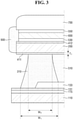
- the frit 310 and the lower and upper coating layers 411 and 412 of the display device 1 according to the current embodiment will now be described in detail by additionally referring to FIG. 3 .
- the term 'frit' refers not only to an additive-containing glass material in the form of a powder but also to a glass structure formed by melting and curing an additive-containing glass material in the form of a powder.
- the frit 310 is be disposed between the light emitting substrate 100 and the encapsulation substrate 200.
- the frit 310 may be a sealing member for bonding the light emitting substrate 100 and the encapsulation substrate 200 together.
- the frit 310 is a glass frit containing a glass material.
- the transmittance of the frit 310 may be smaller than the transmittance of the encapsulation substrate 200.
- the frit 310 may be disposed in the non-display area NA and surround a plurality of light emitting elements 150. In plan view, the frit 310 may be shaped like, but not limited to, a substantially quadrilateral band. The frit 310 may be configured to completely encapsulate the light emitting element 150 together with the encapsulation substrate 200. Accordingly, the damage to the light emitting element 150 due to penetration of moisture or air can be prevented.
- the frit 310 may have inclined side surfaces.
- a lower width W 1 of the frit 310 for example, a width W 1 of the frit 310 on the side of the light emitting substrate 100 may be greater than an upper width W 2 of the frit 310, for example, a width W 2 of the frit 310 on the side of the encapsulation substrate 200.
- the lower width of the frit 310 may be smaller than the upper width of the frit 310, or the side surfaces of the frit 310 may not be inclined, but may be substantially perpendicular.
- a lower surface of the frit 310 may contact the first insulating layer 131 and/or the second insulating layer 133 of the light emitting substrate 100.
- the frit 310 contacts both the first insulating layer 131 and the second insulating layer 133 of the light emitting substrate 100.
- the present disclosure is not limited to this case.
- the frit 310 may not contact the first insulating layer 131, may not contact the second insulating layer 133, or may contact the buffer layer 115 or the base 110.
- an upper surface of the frit 310 may contact the lower coating layer 411. The lower coating layer 411 will be described later.
- the frit 310 may be formed by melting and curing a frit composition or frit paste.
- the frit 310 may include vanadium oxide such as vanadium pentoxide (V 2 O 5 ).
- the content of the vanadium oxide in the frit 310 may be, but is not limited to, about 30 mol% to about 50 mol%.
- the frit 310 may further include a ceramic filler.
- the frit 310 may include barium oxide, bismuth oxide, antimony oxide, borate, phosphate or borosilicate, in addition to vanadium oxide.
- the lower coating layer 411 is disposed between the frit 310 and the encapsulation substrate 200.
- the lower coating layer 411 may be disposed directly on a back surface of the encapsulation substrate 200.
- the lower coating layer 411 may contact the frit 310 and the encapsulation substrate 200.
- the lower coating layer 411 may contribute to the improvement of bond strength between the frit 310 and the encapsulation substrate 200.
- the lower coating layer 411 may be a coating layer formed by single molecules having a self-aligning property or a self-assembling property. That is, the lower coating layer 411 may be a self-aligned layer.
- the lower coating layer 411 may be a self-aligned layer of a polyethylene glycol-based compound.
- the lower coating layer 411 includes a compound having an intramolecular ⁇ -(OCH 2 CH 2 ) n - ⁇ structure (where n is a natural number of 1 to 200) and may be a coating layer formed by self-alignment of the above compound ( ⁇ may be a part of the remaining molecule, and the structure may be alternatively written without the ⁇ ; this also applies to the further definitions herein).
- the compound in the lower coating layer 411 has an intramolecular ⁇ -(OCH 2 CH 2 ) n -OH structure or an intramolecular ⁇ -(OCH 2 CH 2 )-OH structure.
- the compound in the lower coating layer 411 may have an R-(OCH 2 CH2) n -OH structure, where R may be a C 1 -C 50 alkyl group substituted with one or more hydroxyl groups.
- the self-aligned compound having the hydroxyl groups may form a physical/chemical bond with fluorine groups on the back surface of the encapsulation substrate 200.
- the lower coating layer 411 may have alkalinity. As used herein, 'alkalinity' denotes having a pH exceeding 7.
- the lower coating layer 411 may be disposed over the display area DA and the non-display area NA.
- the lower coating layer 411 may overlap the light emitting element 150 in the display area DA and the frit 310 in the non-display area NA in the third direction Z.
- a thickness of the lower coating layer 411 may be approximately uniform.
- a maximum thickness T 1 of the lower coating layer 411 may be about 10 ⁇ m or less. When the maximum thickness T 1 of the lower coating layer 411 is about 10 ⁇ m or less, compounds in the lower coating layer 411 may be stably maintained in a self-aligned state.
- the upper coating layer 412 may be disposed on a front surface of the encapsulation substrate 200.
- the upper coating layer 412 may be disposed directly on the encapsulation substrate 200.
- the upper coating layer 412 may contribute to the improvement of bond strength between the encapsulation substrate 200 and a first bonding layer 530 to be described later.
- the upper coating layer 412 may include the same compound as the lower coating layer 411.
- the upper coating layer 412 may be a self-aligned layer formed by self-alignment of the above-described compound having an intramolecular ⁇ -(OCH 2 CH 2 ) n -OH structure or an intramolecular ⁇ -(OCH 2 CH 2 )-OH structure.
- the self-aligned compound having the hydroxyl groups may form a physical/chemical bond with fluorine groups on the front surface of the encapsulation substrate 200.
- the upper coating layer 412 may have alkalinity.
- the upper coating layer 412 may be disposed over the display area DA and the non-display area NA and may overlap the light emitting element 150 and the frit 310 in the third direction Z.
- a maximum thickness of the upper coating layer 412 may be, but is not limited to, about 10 ⁇ m or less.
- the filler 510 may be disposed between the encapsulation substrate 200 and the light emitting element 150.
- the filler 510 may minimize a step formed by the light emitting element 150, for example, a step formed by the pixel defining layer 160.
- the filler 510 may fill a space between the encapsulation substrate 200 and the light emitting substrate 100. Since the filler 510 minimizes a step difference between the encapsulation substrate 200 and the light emitting substrate 100 and fills the space between the encapsulation substrate 200 and the light emitting substrate 100, the mechanical strength or durability of the display device 1 can be improved.
- the filler 510 may at least partially contact the protective layer 170, the lower coating layer 411, and the frit 310.
- the material of the filler 510 is not particularly limited as long as it is a material having a planarizing property.
- the filler 510 may include an organic material such as acrylic resin, epoxy resin, imide resin, or acrylate resin.
- the filler 510 may not be used or included between the encapsulation substrate 200 and the light emitting element 150, and the encapsulation substrate 200 and the light emitting element 150 may be spaced apart from each other.
- the space between the encapsulation substrate 200 and the light emitting element 150 may be filled with an inert gas such as nitrogen gas (N 2 ).
- the display device 1 may include a functional member 600 disposed on the encapsulation substrate 200, a cover glass 700 disposed on the functional member 600, a housing 800 accommodating the light emitting substrate 100 and the encapsulation substrate 200, and a cushion member 900 disposed on side surfaces of the encapsulation substrate 200.
- the functional member 600 may be disposed on the front surface of the encapsulation substrate 200.
- the functional member 600 may have a polarizing function or a touch sensing function. That is, the functional member 600 may include a polarizing element or a touch sensing element.
- the polarizing element may contribute to outdoor visibility by blocking the transmission of reflected light of external light or at least partially absorbing the reflected light.
- the polarizing element may be a linear polarizer that converts incident light into linearly polarized light or a circular polarizer that converts incident light into circularly polarized light.
- the touch sensing element may sense information input to the display device 1 by a user of the display device 1 through a touch operation.
- the touch operation may be performed using a part of the user's body, a stylus pen, or the like.
- the touch sensing element may sense at least one of information about whether a touch has been made, information about a touch position, information about the magnitude of touch pressure, and information about the shape of an object performing a touch function among the information input by the user.
- the functional member 600 may be a laminated structure of a plurality of layers.
- the first bonding layer 530 may be interposed between the functional member 600 and the upper coating layer 412.
- the first bonding layer 530 may contact a lower surface of the functional member 600 and the upper coating layer 412.
- the first bonding layer 530 may include an optical clear adhesive such as a double-sided tape, an optical clear resin such as a photocurable resin or a thermosetting resin, or a pressure sensitive adhesive.
- the upper coating layer 412 between the encapsulation substrate 200 and the first bonding layer 530 may contribute to the improvement of bond strength between the encapsulation substrate 200 and the first bonding layer 530.
- the cover glass 700 may be disposed on the functional member 600.
- the cover glass 700 may form an upper surface of the display device 1.
- the cover glass 700 may protect the elements inside the display device 1, form a display surface of the display device 1 on which an image is formed, and may form the exterior of the display device 1.
- the cover glass 700 may form a touch surface on which a user's touch operation, that is, a touch operation performed by a user is carried out.
- the cover glass 700 may include a material having high light transmittance and excellent strength such as a glass material, a sapphire material, or a polymer material.
- a second bonding layer 550 may be interposed between the cover glass 700 and the functional member 600.
- the second bonding layer 550 may contact a lower surface of the cover glass 700 and an upper surface of the functional member 600.
- the second bonding layer 550 may include an optical clear adhesive such as a double-sided tape, an optical clear resin such as a photocurable resin or a thermosetting resin, or a pressure sensitive adhesive.
- the second bonding layer 550 may include the same or different material from the first bonding layer 530.
- the housing 800 may be disposed on a back surface of the light emitting substrate 100.
- the housing 800 may have an inner space in which the light emitting substrate 100 and/or the encapsulation substrate 200 can be housed or accommodated. That is, the housing 800 may be a back cover, a back chassis, or a bracket.
- the housing 800 may include a bottom portion 810 which covers the back surface of the light emitting substrate 100 and side portions 830 which protrude upward the bottom portion 810 to cover side surfaces of the light emitting substrate 100 and/or the encapsulation substrate 200.
- the side portions 830 of the housing 800 may protect the base 110 of the light emitting substrate 100 and the encapsulation substrate 200 by covering side surfaces of the base 100 of the light emitting substrate 100 and the encapsulation substrate 200.
- the side portions 830 of the housing 800 may protect the functional member 600 and the cover glass 700 by at least partially covering side surfaces of the functional member 600 and the cover glass 700.
- the bottom portion 810 of the housing 800 may be spaced apart from the base 110, and the side portions 830 of the housing 800 may be spaced apart from the base 110 of the light emitting substrate 100, the encapsulation substrate 200 and the cover glass 700.
- the material of the housing 800 is not particularly limited as long as it is a material having excellent strength and rigidity.
- the housing 800 may include a polymer material such as carbonate resin or a metal material such as aluminum, nickel or an alloy of these metals.
- the cushion member 900 may be disposed on the side surfaces of the encapsulation substrate 200.
- the cushion member 900 may be disposed between the encapsulation substrate 200 and the side portions 830 of the housing 800 to prevent the encapsulation substrate 200 from being damaged by the housing 800.
- the cushion member 900 may maintain the distance between the encapsulation substrate 200 and the housing 800 and absorb at least part of the impact, thereby minimizing damage.
- the cushion member 900 may cover the side surfaces of the encapsulation substrate 200 and may be shaped like a substantially quadrilateral band in plan view.
- the cushion member 900 may contact the encapsulation substrate 200, the first bonding layer 530, the functional member 600, the second bonding layer 550, the cover glass 700, and/or the side portions 830 of the housing 800.
- the cushion member 900 may be coupled to the encapsulation substrate 200, but may be separable from the housing 800.
- the cushion member 900 By aligning the side surfaces of the encapsulation substrate 200, the functional member 600 and the cover glass 700 and maintaining the distance between the encapsulation substrate 200 and the housing 800 using the cushion member 900, it is possible to protect the light emitting substrate 100, the encapsulation substrate 200 and the frit 310 from external impact and minimize a width of the non-display area NA of the display device 1.
- the material of the cushion member 900 is not particularly limited as long as it can absorb at least part of impact.
- the cushion member 900 may include an organic material such as acrylic resin, epoxy resin, imide resin, or acrylate resin.
- the display device 1 may include the lower coating layer 411 and the upper coating layer 412 disposed on the surface of the encapsulation substrate 200.
- the encapsulation substrate 200 including a glass material, the glass frit 310, and the lower coating layer 411 interposed between the encapsulation substrate 200 and the frit 310 form a glass stack. That is, according to the present disclosure, it is possible to provide a glass stack having improved adhesion between a first glass piece (e.g., an encapsulation substrate) and a second glass piece (e.g., a glass frit).
- a first glass piece e.g., an encapsulation substrate
- a second glass piece e.g., a glass frit
- the lower coating layer 411 including a compound having an intramolecular ⁇ -(OCH 2 CH 2 ) n -OH structure or an intramolecular ⁇ -(OCH 2 CH 2 )-OH structure contributes to the improvement of bond strength between the first glass piece (e.g., the encapsulation substrate) and the second glass piece (e.g., the glass frit). Accordingly, the glass stack according to the current embodiment exhibits excellent bond strength.
- the encapsulation substrate 200 including a glass material, the first bonding layer 530 including an organic material, and the upper coating layer 412 interposed between the encapsulation substrate 200 and the first bonding layer 530 may form a glass-resin stack. That is, according to the present disclosure, it is possible to provide a glass-resin stack having improved adhesion between glass and resin.
- the upper coating layer 412 including a compound having an intramolecular ⁇ -(OCH 2 CH 2 ) n -OH structure or an intramolecular ⁇ -(OCH 2 CH 2 )-OH structure may contribute to the improvement of bond strength between the encapsulation substrate 200 and the first bonding layer 530. Accordingly, the glass-resin stack according to the present embodiment may exhibit excellent bond strength.
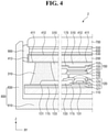
- FIG. 4 is a cross-sectional view of a display device 2 according to an embodiment, illustrating a display area where a light emitting element 150 of the display device 2 is disposed and a non-display area where a frit 310 is disposed.
- FIG. 5 is an enlarged cross-sectional view of the non-display area of the display device 2 of FIG. 4 .
- the display device 2 according to the current embodiment is different from the display device 1 according to the embodiment of FIG. 2 , etc. in that it further includes a side coating layer 413 disposed on side surfaces of an encapsulation substrate 200.
- the side coating layer 413 may be disposed between the encapsulation substrate 200 and a cushion member 900.
- the side coating layer 413 may be disposed directly on the side surfaces of the encapsulation substrate 200.
- the side coating layer 413 may contribute to the improvement of bond strength between the encapsulation substrate 200 and the cushion member 900.
- the side coating layer 413 may include the same compound as a lower coating layer 411 and an upper coating layer 412.
- the side coating layer 413 may be a self-aligned layer formed by self-alignment of the above-described compound having an intramolecular ⁇ -(OCH 2 CH 2 ) n -OH structure or an intramolecular ⁇ -(OCH 2 CH 2 )-OH structure.
- the self-aligned compound having the hydroxyl groups may form a physical/chemical bond with fluorine groups on the side surfaces of the encapsulation substrate 200.
- a physical boundary that is visible with the naked eye may not substantially exist between the side coating layer 413 and the lower coating layer 411 and between the side coating layer 413 and the upper coating layer 412.
- the side coating layer 413 may have alkalinity.
- a maximum thickness of the side coating layer 413 may be, but is not limited to, about 10 ⁇ m or less.
- the side coating layer 413 may include a different compound from the lower coating layer 411 and the upper coating layer 412.
- the cushion member 900 may be disposed on the side coating layer 413.
- the cushion member 900 may contact the side coating layer 413, a first bonding layer 530, a functional member 600, a second bonding layer 550, a cover glass 700 and/or side portions 830 of a housing 800.
- the encapsulation substrate 200 including a glass material, the cushion member 900 including an organic material, and the side coating layer 413 interposed between the encapsulation substrate 200 and the cushion member 900 may form a glass-resin stack.
- FIG. 6 is a cross-sectional view of a display device 3 according to an embodiment, illustrating a display area where a light emitting element 150 of the display device 3 is disposed and a non-display area where a frit 330 is disposed.
- FIG. 7 is an enlarged cross-sectional view of the non-display area of the display device 3 of FIG. 6 .
- the display device 3 according to the current embodiment is different from the display device 2 according to the embodiment of FIG. 4 , etc. in that a lower coating layer 431 has a partially different thickness.
- the lower coating layer 431 may overlap the light emitting element 150 in the display area and the frit 330 in the non-display area in the third direction Z.
- an average thickness of the lower coating layer 431 overlapping the light emitting element 150 may be greater than an average thickness of the lower coating layer 431 overlapping the frit 330.
- a first thickness T 2 of the lower coating layer 431 overlapping the light emitting element 150 in the display area may be substantially uniform.
- the first thickness T 2 may be about 10 ⁇ m or less.
- a thickness of the lower coating layer 431 overlapping the frit 330 in the non-display area may be partially non-uniform.
- a portion of the lower coating layer 431 which overlaps the frit 330 may have a second thickness T 3 smaller than the first thickness T 2 .
- a portion of the lower coating layer 431 which contacts the frit 330 may have the second thickness T 3 .
- An upper limit of the second thickness T 3 may be about 5.0 ⁇ m, about 4.0 ⁇ m, about 3.0 ⁇ m, about 2.0 ⁇ m, or about 1.0 ⁇ m. Therefore, an inclined surface may be formed on part of a surface of the lower coating layer 431.
- the lower coating layer 431 which contacts the frit 330 of the display device 3 may have a partially non-uniform thickness.
- the lower coating layer 431 contacting the frit 330 may be formed relatively thin so that the lower coating layer 431 can form a partially inclined surface while a compound having an intramolecular ⁇ -(OCH 2 CH 2 ) n -OH structure or an intramolecular ⁇ -(OCH 2 CH 2 )-OH structure is stably maintained in a self-aligned state.
- the inclined surface of the lower coating layer 431 may increase the area of a bonding interface between the frit 330 and the lower coating layer 431, thereby further improving the bond strength formed by the frit 330.
- the inclined surface of the lower coating layer 431 may increase a path length of the bonding interface between the frit 330 and the lower coating layer 431, thereby increasing a length of a penetration path of impurities such as moisture or air.
- a side coating layer 413 may be omitted, and a cushion member 900 may contact an encapsulation substrate 200.
- FIG. 8 is a cross-sectional view of a display device 4 according to an embodiment, illustrating a display area where a light emitting element 150 of the display device 4 is disposed and a non-display area where a frit 340 is disposed.
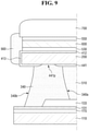
- FIG. 9 is an enlarged cross-sectional view of the non-display area of the display device 4 of FIG. 8 .
- the display device 4 according to the current embodiment is different from the display device 2 according to the embodiment of FIG. 4 , etc. in that at least a portion of the frit 340 contacts an encapsulation substrate 200.
- a lower coating layer 441 may have an opening 441p that at least partially exposes a back surface of the encapsulation substrate 200.
- the opening 441p of the lower coating layer 441 may be formed in the process of forming the frit 340 by melting and curing a frit composition or frit paste, but the present disclosure is not limited to this case.
- the opening 441p of the lower coating layer 441 may be controlled by the type of laser, the position of laser focus, laser irradiation intensity, or laser irradiation time.
- the frit 340 may at least partially contact the lower coating layer 441 and may further contact the encapsulation substrate 200 exposed by the opening 441p. For example, an approximately central portion of an upper surface of the frit 340 may contact the encapsulation substrate 200 in plan view.
- each of an inner edge portion formed by the upper surface and inner side surface 340a of the frit 340 and an outer edge portion formed by the upper surface and outer side surface 340b of the frit 340 may contact the lower coating layer 441.
- the inner side surface 340a of the frit 340 may be a side surface on the side of the light emitting elements 150
- the outer side surface 340b of the frit 340 may be a side surface opposite the inner side surface 340a.
- a bonding interface may be formed between the frit 340 and the encapsulation substrate 200, and the penetration of impurities such as moisture or air through the bonding interface formed between the frit 340 and the encapsulation substrate 200 in contact with each other can be effectively prevented.
- a side coating layer 413 may be omitted, and a cushion member 900 may contact the encapsulation substrate 200.
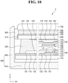
- FIG. 10 is a cross-sectional view of a display device 5 according to an embodiment, illustrating a display area where a light emitting element 150 of the display device 5 is disposed and a non-display area where a frit 350 is disposed.
- FIG. 11 is an enlarged cross-sectional view of the non-display area of the display device 5 of FG. 10.
- the display device 5 according to the current embodiment is different from the display device 2 according to the embodiment of FIG. 4 , etc. in that an outer edge portion of the frit 350 contacts an encapsulation substrate 200.
- a lower coating layer 451 may be disposed on a back surface of the encapsulation substrate 200, but may not be disposed in an edge region of the back surface of the encapsulation substrate 200 in plan view.
- a region where the lower coating layer 451 is not disposed may be controlled in the process of forming the frit 350, but the present disclosure is not limited to this case.
- the region where the lower coating layer 451 of the frit 350 is not disposed may be controlled by, for example, the laser irradiation position.
- the frit 350 may at least partially contact the lower coating layer 451 and may further contact the encapsulation substrate 200 uncovered by the lower coating layer 451.
- An inner edge portion formed by an upper surface and an inner side surface 350a of the frit 350 may contact the lower coating layer 451.
- the outer edge portion formed by an approximately central portion of the upper surface of the frit 350, the upper surface of the frit 350, and an outer side surface 350b of the frit 350 may contact the encapsulation substrate 200.
- the bonding surface When an impact is applied from the outside of the display device 5, stress may be concentrated on a bonding surface formed by the frit 350, thereby damaging the bonding surface.
- the bonding surface may be relatively more vulnerable to damage near the inner edge portion of the frit 350 than near the outer edge portion of the frit 350.
- the bonding strength can be improved.
- the frit 350 and the encapsulation substrate 200 are formed to partially contact each other, specifically, since the outer edge portion of the frit 350 and the central portion of the upper surface of the frit 350 are formed to contact the encapsulation substrate 200, a bonding interface may be formed between the frit 350 and the encapsulation substrate 200, and the penetration of impurities such as moisture or air through the bonding interface formed between the frit 350 and the encapsulation substrate 200 in contact with each other can be effectively prevented.
- an average inclination angle ⁇ 1 of the inner side surface 350a of the frit 350 and an average inclination angle ⁇ 2 of the outer side surface 350b of the frit 350 may be different.
- the average inclination angle ⁇ 1 of the inner side surface 350a of the frit 350 and the average inclination angle ⁇ 2 of the outer side surface 350b of the frit 350 may all be 90 degrees or less, but the average inclination angle ⁇ 1 of the inner side surface 350a of the frit 350 may be smaller than the average inclination angle ⁇ 2 of the outer side surface 350b of the frit 350.
- the average inclination angle ⁇ 1 of the inner side surface 350a of the frit 350 may be about 60 degrees to about 80 degrees, and the average inclination angle ⁇ 2 of the outer side surface 350b of the frit 350 may be about 65 degrees to about 88 degrees.
- the inclination angles ⁇ 1 and ⁇ 2 of the inner side surface 350a and the outer side surface 350b of the frit 350 may be controlled in the process of melting and curing a frit composition or frit paste, but the present disclosure is not limited to this case.
- the inclination angles ⁇ 1 and ⁇ 2 of the inner side surface 350a and the outer side surface 350b of the frit 350 may be controlled by, for example, the laser irradiation position.
- a side coating layer 413 may be omitted, and a cushion member 900 may contact the encapsulation substrate 200.
- FIG. 12 is a cross-sectional view of a display device 6 according to an embodiment, illustrating a display area where a light emitting element 150 of the display device 6 is disposed and a non-display area where a frit 360 is disposed.
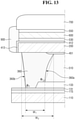
- FIG. 13 is an enlarged cross-sectional view of the non-display area of the display device 6 of FIG. 12 .
- the display device 6 according to the current embodiment is different from the display device 5 according to the embodiment of FIG. 10 , etc. in that the frit 360 has inclined surfaces and a lower width W 1 of the frit 360, for example, a width W 1 of the frit 360 on the side of a light emitting substrate is smaller than an upper width W 2 of the frit 360, for example, a width W 2 of the frit 360 on the side of an encapsulation substrate 200.
- an average inclination angle ⁇ 1 of an inner side surface 360a of the frit 360 and an average inclination angle ⁇ 2 of an outer side surface 360b of the frit 360 may be different.
- the average inclination angle ⁇ 1 of the inner side surface 360a of the frit 360 and the average inclination angle ⁇ 2 of the outer side surface 360b of the frit 360 may all be 90 degrees or more, but the average inclination angle ⁇ 1 of the inner side surface 360a of the frit 360 may be greater than the average inclination angle ⁇ 2 of the outer side surface 360b of the frit 360.
- the inclination angles ⁇ 1 and ⁇ 2 of the inner side surface 360a and the outer side surface 360b of the frit 360 may be controlled in the process of melting and curing a frit composition or frit paste, but the present disclosure is not limited to this case.
- a side coating layer 413 may be omitted, and a cushion member 900 may contact the encapsulation substrate 200.
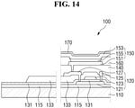
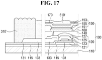
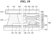
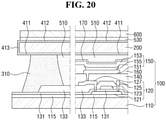
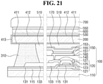
- FIGS. 14 through 23 are cross-sectional views illustrating a method of manufacturing a display device according to an embodiment.
- a light emitting substrate 100 including a base 110, a thin-film transistor 120, a light emitting element 150, and a protective layer 170 is prepared. Since the elements of the light emitting substrate 100 have been described above, a redundant description thereof is omitted.
- a surface of the encapsulation substrate 200 is treated with fluorine.
- a first surface (a lower surface in FIG. 15 ) and a second surface (an upper surface in FIG. 15 ) of the encapsulation substrate 200 are treated with fluorine to form fluorine groups (-F) on the first and second surfaces of the encapsulation substrate 200.
- side surfaces of the encapsulation substrate 200 may also be treated with fluorine.
- the encapsulation substrate 200 having lower and upper coating layers 411 and 412 formed on at least a portion of its surface is prepared.
- the preparing of the encapsulation substrate 200 having the lower and upper coating layers 411 and 412 may include forming the lower coating layer 411 on the fluorine group-containing first surface (the lower surface in FIG. 15 ) of the encapsulation substrate 200, forming the upper coating layer 412 on the fluorine group-containing second surface (the upper surface in FIG. 15 ) of the encapsulation substrate 200, and washing and drying the encapsulation substrate 200 having the lower coating layer 411 and the upper coating layer 412.
- lower coating layer 411 may include self-aligning single molecules having a self-aligning property or a self-assembling property directly on the encapsulation substrate 200.
- lower coating layer 411 is a coating layer formed by self-alignment of a compound having an intramolecular ⁇ -(OCH 2 CH 2 ) n -OH structure or an intramolecular ⁇ -(OCH 2 CH 2 )-OH structure. Since the above compound has been described above, a redundant description thereof is omitted.
- the forming of the upper coating layer 412 may include self-aligning single molecules having a self-aligning property or a self-assembling property directly on the encapsulation substrate 200.
- the upper coating layer 412 may include the same compound as the lower coating layer 411, and thus a redundant description thereof is omitted.
- the lower coating layer 411 and the upper coating layer 412 may be simultaneously formed through a single process.
- the washing and drying of the encapsulation substrate 200 having the lower coating layer 411 and the upper coating layer 412 may include washing the encapsulation substrate 200 using distilled water or deionized water and drying the washed encapsulation substrate 200 using an air knife.
- the lower coating layer 411 and the upper coating layer 412 that are substantially water-insoluble may be stabilized in the process of being washed by an aqueous medium. That is, since the encapsulation substrate 200 is washed after the lower coating layer 411 and the upper coating layer 412 are formed on the encapsulation substrate 200, the lower coating layer 411 and the upper coating layer 412 can be made more solid.
- a frit composition 310' and a filler composition 510' are provided on the light emitting substrate 100 and are heat-treated.
- the providing of the frit composition 310' may be an operation of applying the frit composition 310' onto the light emitting substrate 100.
- the applying method is not particularly limited, but, e.g., screen printing may be used.
- the frit composition 310' may be provided in a substantially quadrilateral band shape along edges of the light emitting substrate 100.
- the frit composition 310' may include vanadium oxide and further include a ceramic filler or an organic material and may be in a paste or gel state.
- the heat-treating of the frit composition 310' may be an operation of pre-curing the frit composition 310' in the paste or gel state to a solid state by baking the frit composition 310'.
- the frit composition 310' pre-cured or baked through heat treatment may be temporarily fixed on the light emitting substrate 100 in a substantially solid state. In this operation, the organic material in the frit composition 310' may be removed through deterioration, but the present disclosure is not limited to this case.
- the heat-treating of the filler composition 510' may be an operation of curing the filler composition 510'.
- the heat treatment temperature of the frit composition 310' and the filler composition 510' may be about 300 ⁇ to about 500 ⁇ or about 350 ⁇ to about 450 ⁇ .
- the heat treatment operation may be performed under a nitrogen atmosphere.
- the frit composition 310' and the filler composition 510' are provided on the light emitting substrate 100 and are treated with heat.
- the present disclosure is not limited to this case.
- the frit composition 310' and/or the filler composition 510' may be provided on the encapsulation substrate (not illustrated).
- the providing of the filler composition 510' may be omitted, and a space surrounded by the light emitting substrate 100, the encapsulation substrate 200, and a frit 310 to be described later may be filled with an inert gas such as nitrogen gas (N 2 ).
- an inert gas such as nitrogen gas (N 2 ).
- the frit 310 is formed between the light emitting substrate 100 and the encapsulation substrate 200 to bond the light emitting substrate 100 and the encapsulation substrate 200 together.
- the forming of the frit 310 may include aligning the light emitting substrate 100 and the encapsulation substrate 200 and forming the frit 310 by melting and curing the heat-treated frit composition 310'.
- the aligning of the light emitting substrate 100 and the encapsulation substrate 200 may be an operation of aligning the light emitting substrate 100 and the encapsulation substrate 200 such that the frit composition 310' pre-cured or baked through heat treatment overlaps the lower coating layer 411 and the upper coating layer 412.
- the melting and curing of the heat-treated frit composition 310' may include irradiating a laser L to the frit composition 310' pre-cured or baked through heat treatment.
- the laser L irradiated to the heat-treated frit composition 310' may melt the frit composition 310'.
- the frit composition 310' melted after being irradiated with the laser L may be cured or re-cured to form the frit 310.
- the laser L may be irradiated to the frit composition 310' sequentially via the upper coating layer 412, the encapsulation substrate 200, and the lower coating layer 411.
- the frit 310 may contact a first insulating layer 131 and a second insulating layer 133 of the light emitting substrate 100 and the lower coating layer 411 to form a bonding interface.
- the lower coating layer 411 between the encapsulation substrate 200 and the frit 310 may contribute to the improvement of bond strength between the encapsulation substrate 200 and the frit 310.
- the laser L may have a wavelength of about 760 nm to about 860 nm or about 780 nm to about 830 nm.
- the laser L may be irradiated while being moved along the shape of the frit composition 310' which is temporarily fixed as a result of being pre-cured or baked.
- the energy distribution of the laser L may have a flat shape, not a Gaussian distribution, but the present disclosure is not limited to this case.
- the side surfaces of the encapsulation substrate 200 may be exposed after the light emitting substrate 100 and the encapsulation substrate 200 are bonded together.
- a side coating layer 413 is formed on the side surfaces of the encapsulation substrate 200.
- the forming of the side coating layer 413 may include self-aligning single molecules having a self-aligning property or a self-assembling property directly on the side surfaces of the encapsulation substrate 200.
- the side coating layer 413 may include the same compound as the lower coating layer 411 and the upper coating layer 412, that is, the compound having the intramolecular ⁇ -(OCH 2 CH 2 ) n -OH structure or the intramolecular ⁇ -(OCH 2 CH 2 )-OH structure. Thus, a redundant description of the compound of the side coating layer 413 is omitted.
- the method of manufacturing a display device may further include partially washing and drying the light emitting substrate 100 and the encapsulation substrate 200 bonded together.
- the washing and drying of the light emitting substrate 100 and the encapsulation substrate 200 may include washing the light emitting substrate 100 and the encapsulation substrate 200 using distilled water or deionized water and drying the light emitting substrate 100 and the encapsulation substrate 200 using an air knife.
- a functional member 600 is formed on the encapsulation substrate 200 with a first bonding layer 530 interposed between the functional member 600 and the encapsulation substrate 200. Since the first bonding layer 530 and the functional member 600 have been described above, a redundant description thereof is omitted.
- a cover glass 700 is formed on the functional member 600 with a second bonding layer 550 interposed between the cover glass 700 and the functional member 600. Since the second bonding layer 550 and the cover glass 700 have been described above, a redundant description thereof is omitted.
- a cushion member 900 is formed.
- the cushion member 900 may be disposed on the side surfaces of the encapsulation substrate 200.
- the cushion member 900 may at least partially contact the side coating layer 413, the first bonding layer 530, the functional member 600, the second bonding layer 550, and the cover glass 700. Since the cushion member 900 has been described above, a redundant description thereof is omitted.
- the light emitting substrate 100 and the encapsulation substrate 200 are inserted into a housing 800. Since the housing 800 has been described above, a redundant description thereof is omitted.
- a coating layer capable of improving bond strength is interposed between an encapsulation substrate or a glass and a frit to improve the bond strength between the encapsulation substrate or the glass and the frit.
Landscapes
- Engineering & Computer Science (AREA)
- Chemical & Material Sciences (AREA)
- Physics & Mathematics (AREA)
- Life Sciences & Earth Sciences (AREA)
- Materials Engineering (AREA)
- Organic Chemistry (AREA)
- Chemical Kinetics & Catalysis (AREA)
- General Chemical & Material Sciences (AREA)
- Geochemistry & Mineralogy (AREA)
- General Physics & Mathematics (AREA)
- Theoretical Computer Science (AREA)
- Optics & Photonics (AREA)
- General Engineering & Computer Science (AREA)
- Ceramic Engineering (AREA)
- Human Computer Interaction (AREA)
- Wood Science & Technology (AREA)
- Computer Hardware Design (AREA)
- Manufacturing & Machinery (AREA)
- Electroluminescent Light Sources (AREA)
- Devices For Indicating Variable Information By Combining Individual Elements (AREA)
Description
- The present disclosure relates to a display device, a method of manufacturing the same, and a glass stack.
- With the development of multimedia, display devices are becoming increasingly important. Accordingly, various display devices such as liquid crystal displays and organic light emitting diode displays are being developed.
- For example, an organic light emitting display includes a base and an organic light emitting element disposed on the base. The organic light emitting element may include two opposite electrodes and an organic light emitting layer interposed between the two opposite electrodes. Electrons and holes provided from the two electrodes may be recombined in the organic light emitting layer to generate excitons, and the generated excitons may emit light as they change from an excited state to a ground state. The organic light emitting layer of the organic light emitting element is vulnerable to damage by moisture or air.
- As one way to suppress the damage of the organic light emitting layer due to external moisture or air, a method of placing an encapsulation substrate on a light emitting substrate including a light emitting element and then bonding the light emitting substrate and the encapsulation substrate together using a frit material may be exemplified.
- There is a limit in improving the bond strength between an encapsulation substrate and a frit. For example, when an impact is applied from the outside of a display device, a bonding surface between the encapsulation substrate and the frit may be damaged. If the bonding surface between the encapsulation substrate and the frit is damaged, penetration of moisture, air, or the like from the outside may be allowed, thereby reducing the durability of an organic light emitting element.
-
US6887577B1 describes a laminated safety glass comprising two panes of glass and an intermediate film based on PVB comprising a polyethylene glycol plasticizer to improve sound insulation.US2009/0206739A1 andEP1814178A2 describe an OLED display device comprising a frit material between a base substrate and an encapsulation substrate. - Aspects of the present disclosure provide a display device having improved bond strength between an encapsulation substrate and a frit.
- Aspects of the present disclosure also provide a method of manufacturing a display device, the method being employed to improve the bond strength between an encapsulation substrate and a frit.
- Aspects of the present disclosure also provide a glass stack having improved bond strength.
- However, aspects of the present disclosure are not restricted to the one set forth herein. The above and other aspects of the present disclosure will become more apparent to one of ordinary skill in the art to which the present disclosure pertains by referencing the detailed description of the present disclosure given below.
- According to the claimed invention, a display device is as recited in
claim 1, a glass stack as recited in claim 16 and a method of manufacturing a display device as recited in claim 17. - Further details are described in dependent claims.
- These and/or other aspects will become apparent and more readily appreciated from the following description of the embodiments, taken in conjunction with the accompanying drawings in which:
-
FIG. 1 is a perspective view of a display device according to an embodiment; -
FIG. 2 is a cross-sectional view of a display area and a non-display area of the display device ofFIG. 1 ; -
FIG. 3 is an enlarged cross-sectional view of the non-display area of the display device ofFIG. 2 ; -
FIG. 4 is a cross-sectional view of a display device according to an embodiment; -
FIG. 5 is an enlarged cross-sectional view of the non-display area of the display device ofFIG. 4 ; -
FIG. 6 is a cross-sectional view of a display device according to an embodiment; -
FIG. 7 is an enlarged cross-sectional view of the non-display area of the display device ofFIG. 6 ; -
FIG. 8 is a cross-sectional view of a display device according to an embodiment; -
FIG. 9 is an enlarged cross-sectional view of the non-display area of the display device ofFIG. 8 ; -
FIG. 10 is a cross-sectional view of a display device according to an embodiment; -
FIG. 11 is an enlarged cross-sectional view of the non-display area of the display device of FG. 10; -
FIG. 12 is a cross-sectional view of a display device according to an embodiment; -
FIG. 13 is an enlarged cross-sectional view of the non-display area of the display device ofFIG. 12 ; and -
FIGS. 14 through 23 are cross-sectional views illustrating a method of manufacturing a display device according to an embodiment. - Features of the inventive concept and methods of accomplishing the same may be understood more readily by reference to the following detailed description of embodiments and the accompanying drawings. The inventive concept may, however, be embodied in many different forms and should not be construed as being limited to the embodiments set forth herein. Rather, these embodiments are provided so that this disclosure will be thorough and complete and will fully convey the concept of the inventive concept to those skilled in the art, and the inventive concept will only be defined by the appended claims. Like reference numerals refer to like elements throughout the specification.
- The terminology used herein is for the purpose of describing particular embodiments only and is not intended to be limiting of the inventive concept. As used herein, the singular forms "a", "an" and "the" are intended to include the plural forms as well, unless the context clearly indicates otherwise. It will be further understood that the terms "comprises" and/or "comprising," when used in this specification, specify the presence of stated features, integers, steps, operations, elements, and/or components, but do not preclude the presence or addition of one or more other features, integers, steps, operations, elements, components, and/or groups thereof.
- It will be understood that when an element or layer is referred to as being "on", "connected to" or "coupled to" another element or layer, it can be directly on, connected or coupled to the other element or layer or intervening elements or layers may be present. In contrast, when an element is referred to as being "directly on", "directly connected to" or "directly coupled to" another element or layer, there are no intervening elements or layers present. As used herein, the term "and/or" includes any and all combinations of one or more of the associated listed items.
- It will be understood that, although the terms first, second, etc. may be used herein to describe various elements, components, regions, layers and/or sections, these elements, components, regions, layers and/or sections should not be limited by these terms. These terms are only used to distinguish one element, component, region, layer or section from another region, layer or section. Thus, a first element, component, region, layer or section discussed below could be termed a second element, component, region, layer or section without departing from the teachings of the inventive concept.
- As used herein, a first direction X denotes any one direction in a plane, a second direction Y denotes a direction intersecting the first direction X in the plane, and a third direction Z denotes a direction perpendicular to the plane. Unless otherwise defined, 'plane' refers to a plane to which the first direction X and the second direction Y belong.
- Hereinafter, embodiments will be described with reference to the accompanying drawings.
-
FIG. 1 is a perspective view of adisplay device 1 according to an embodiment. - Referring to
FIG. 1 , thedisplay device 1 according to the current embodiment may include a display area DA and a non-display area NA. - The display area DA may be an area contributing to substantial image display by including a plurality of pixels PX. As used herein, 'pixels' refer to single regions into which the display area DA is divided for color display in plan view, and one pixel may be a single region defined as a minimum unit that can express a color independently of other pixels. That is, each of the pixels PX may uniquely display one of predetermined primary colors to implement color display. Examples of the primary colors include red, green and blue. In plan view, the display area DA may be surrounded by the non-display area NA. The non-display area DA does not contribute to image display, and elements necessary for the operation of the
display device 1 may be located in the non-display area NA. - The
display device 1 according to the current embodiment will now be described in more detail by additionally referring toFIG. 2. FIG. 2 is a cross-sectional view of the display area DA and the non-display area NA of thedisplay device 1 ofFIG. 1 , illustrating a region where alight emitting element 150 is disposed and a region where afrit 310 is disposed. - Referring to
FIGS. 1 and2 , thedisplay device 1 may include alight emitting substrate 100, anencapsulation substrate 200 and the frit 310 bonding thelight emitting substrate 100 and theencapsulation substrate 200 together and may further include lower and upper coating layers 411 and 412 disposed on at least part of a surface of the encapsulatingsubstrate 200. The lower and upper coating layers 411 and 412 may also be termed as first and second coating layers 411 and 412. - The
light emitting substrate 100 may include abase 110 and thelight emitting element 150. Thelight emitting substrate 100 may include thelight emitting element 150 capable of emitting light by itself to provide light required for image display. For example, thelight emitting substrate 100 may be a display substrate including thelight emitting element 150 disposed in each pixel PX. Thelight emitting elements 150 respectively disposed in the pixels PX may emit light independently of each other, thereby realizing image display and color display. - The base 110 may be a transparent or opaque insulating substrate or film. For example, the
base 110 may include a glass material or a quartz material or may include a polymer material such as polyimide, polycarbonate, polyethylene terephthalate or polyacrylate. - A
buffer layer 115 may be disposed on a surface (an upper surface inFIG. 2 ) of thebase 110. Thebuffer layer 115 may protect thebase 110 and prevent impurities such as moisture or air from penetrating and damaging thelight emitting element 150. In addition, thebuffer layer 115 may prevent the base 110 from being damaged in the process of forming anactive layer 121 which will be described later. Thebuffer layer 115 may be disposed over the display area DA and the non-display area NA. Thebuffer layer 115 may include an inorganic material such as silicon nitride (SiNx), silicon oxide (SiOx), or silicon nitride oxide (SiNxOy, SiOxNy). In an embodiment, thebuffer layer 115 may be omitted. - A thin-
film transistor 120 and first and second insulatinglayers buffer layer 115. - The thin-
film transistor 120 may be a driving transistor configured to control the amount of light emitted from thelight emitting element 150 in a certain pixel PX by controlling the amount of current flowing through a channel region in theactive layer 121 according to a signal transmitted to a control terminal. For example, the thin-film transistor 120 may include theactive layer 121 that forms a channel, agate 123 which is the control terminal, adrain 125 which is an input terminal, and asource 127 which is an output terminal. - The
active layer 121 may be disposed on thebuffer layer 115. Theactive layer 121 may include a semiconductor material. For example, theactive layer 121 may include polycrystalline silicon. In an embodiment, theactive layer 121 may include monocrystalline silicon or amorphous silicon or may include a non-silicon-based semiconductor material such as an oxide semiconductor. Theactive layer 121 may be partially conductive. For example, theactive layer 121 may include a drain region and a source region spaced apart from each other by the channel region interposed between the drain region and the source region, and each of the drain region and the source region may have greater electrical conductivity than the channel region. - The
gate 123 may be disposed on theactive layer 121. Thegate 123 may at least partially overlap the channel region of theactive layer 121. Thegate 123 may include aluminum (Al), molybdenum (Mo), copper (Cu), or an alloy of these materials. Although not illustrated in the drawings, thegate 123 may be electrically connected to an output electrode of a switching transistor (not illustrated) that controls ON/OFF of a certain pixel. - The first
gate insulating layer 131 may be interposed between theactive layer 121 and thegate 123 to insulate theactive layer 121 and thegate 123 from each other. That is, the first insulatinglayer 131 may be a gate insulating layer. The first insulatinglayer 131 may be disposed over the display area DA and the non-display area NA. The first insulatinglayer 131 may include an inorganic insulating material such as silicon nitride, silicon oxide, or silicon nitride oxide. - The second
insulating layer 133 may be disposed on thegate 123. The secondinsulating layer 133 may insulate thegate 123 from elements disposed on thegate 123. The secondinsulating layer 133 may be disposed over the display area DA and the non-display area NA. In some embodiments, the second insulatinglayer 133 may be a laminated structure of a plurality of insulating layers. The secondinsulating layer 133 may include an inorganic insulating material such as silicon nitride, silicon oxide, or silicon nitride oxide. - Through holes at least partially exposing the
active layer 121 may be formed in the first insulatinglayer 131 and the second insulatinglayer 133. For example, the through holes may pass through the first insulatinglayer 131 and the second insulatinglayer 133 to at least partially expose the drain region and the source region of theactive layer 121. - The
drain 125 and thesource 127 may be disposed on the second insulatinglayer 133. Thedrain 125 and thesource 127 may be respectively inserted into the through holes to contact theactive layer 121. Although not illustrated in the drawings, thedrain 125 may be electrically connected to a driving voltage line (not illustrated) to receive a driving voltage, and thesource 127 may be electrically connected to thelight emitting element 150. - A step
difference compensating layer 140 may be disposed on thedrain 125 and thesource 127. The stepdifference compensating layer 140 may minimize steps formed by elements such as the thin-film transistor 120, the switching transistor (not illustrated), auxiliary electrodes (not illustrated) and/or wirings (not illustrated) such as a scan line, a data line and the driving voltage line. That is, the stepdifference compensating layer 140 may be a planarizing layer that provides a space in which thelight emitting element 150 can be stably disposed. The material of the stepdifference compensating layer 140 is not particularly limited as long as it has an insulating property and a planarizing property. For example, the stepdifference compensating layer 140 may include an organic or inorganic material such as acrylic resin, epoxy resin, imide resin, cardo resin, or ester resin. - The
light emitting element 150 may be disposed on the stepdifference compensating layer 140. Thelight emitting element 150 may be disposed in each pixel PX. For example, thelight emitting element 150 may be an organic light emitting element including ananode 151 and acathode 153 which face each other and an organiclight emitting layer 155 which is interposed between theanode 151 and thecathode 153. Thelight emitting element 150 may emit blue light, green light, red light, or white light depending on the material or the lamination structure of the organiclight emitting layer 155. - The
anode 151 may be disposed on the stepdifference compensating layer 140. Theanode 151 may be electrically connected to thesource 127 through a through hole penetrating the stepdifference compensating layer 140. InFIG. 2 , etc., theanode 151 and thesource 127 of the thin-film transistor 120 (i.e., the driving transistor) are in direct contact with each other and thus are directly connected to each other. However, the present disclosure is not limited to this case, and theanode 151 and thesource 127 can be electrically connected by one or more thin-film transistors (not illustrated) or a connection electrode (not illustrated). Theanode 151 may be a pixel electrode which is disposed in each pixel PX in the display area DA and to which an independent driving signal is transmitted. Theanode 151 may be a transparent electrode, an opaque electrode, or a laminated structure of a transparent electrode and an opaque electrode. Examples of the material that forms the transparent electrode include indium tin oxide (ITO), indium zinc oxide (IZO), zinc oxide, and indium oxide. Examples of the material that forms the opaque electrode include lithium (Li), aluminum (Al), magnesium (Mg), silver (Ag), nickel (Ni), and chromium (Cr). - The
cathode 153 may be disposed on theanode 151. Thecathode 153 may be a common electrode disposed over or across a plurality of pixels PX without distinction between the pixels PX. That is, a plurality oflight emitting elements 150 disposed in different pixels PX may share thecathode 153 with each other. Like theanode 151, thecathode 153 may be a transparent electrode, an opaque electrode, or a laminated structure of a transparent electrode and an opaque electrode. - The organic
light emitting layer 155 may be interposed between theanode 151 and thecathode 153. The organiclight emitting layer 155 may emit light by recombining holes and electrons received from theanode 151 and thecathode 153. For example, electrons and holes may be recombined in the organiclight emitting layer 155 to generate excitons, and the generated excitons may emit light as they change from an excited state to a ground state. - The organic
light emitting layer 155 may include a material that can emit blue phosphorescent or fluorescent light having a peak wavelength in the range of about 430 nm (nanometer) to about 470 nm, a material that can emit green phosphorescent or fluorescent light having a peak wavelength in the range of about 530 nm to about 570 nm, or a material that can emit red phosphorescent or fluorescent light having a peak wavelength in the range of about 610 nm to about 650 nm. InFIG. 2 , etc., the organiclight emitting layer 155 is disposed in each pixel PX. However, the present disclosure is not limited to this case. In an embodiment, the organiclight emitting layer 155 may be disposed over a plurality of pixels PX. That is, at least some of a plurality oflight emitting elements 150 disposed in different pixels PX may share the organiclight emitting layer 155 with each other. - Although not illustrated in the drawings, hole control assisting layers (not illustrated) such as a hole injection layer, a hole transport layer and a hole blocking layer, electron control assisting layers (not illustrated) such as an electron injection layer, an electron transport layer and an electron blocking layer, or a charge generation assisting layer (illustrated) may be further formed between the organic
light emitting layer 155 and theanode 151 or between the organiclight emitting layer 155 and thecathode 153 to improve the luminous efficiency of thelight emitting element 150. - In some embodiments, a
pixel defining layer 160 may be disposed on theanode 151. Thepixel defining layer 160 may define each pixel PX in the display area DA. Thepixel defining layer 160 may have an opening that partially exposes a surface of theanode 151. That is, in plan view, thepixel defining layer 160 may have an opening that exposes at least a portion of theanode 151 disposed in each pixel PX. The organiclight emitting layer 155 and thecathode 153 described above may be disposed on thepixel defining layer 160. Thepixel defining layer 160 may include an organic material such as acrylic resin, epoxy resin, imide resin, or ester resin. - The
light emitting substrate 100 may further include aprotective layer 170 disposed on thelight emitting element 150. Theprotective layer 170 may be disposed directly on thelight emitting element 150. For example, theprotective layer 170 may be disposed directly on thecathode 153 of thelight emitting element 150. Together with theencapsulation substrate 200 and the frit 310 which will be described later, theprotective layer 170 may prevent impurities such as moisture or air from penetrating and damaging thelight emitting element 150 or prevent thelight emitting element 150 from being damaged by afiller 510 containing an organic material. That is, theprotective layer 170 may perform an additional encapsulating function for thelight emitting element 150. Theprotective layer 170 may be disposed over a plurality of pixels PX. Theprotective layer 170 may include an inorganic material such as silicon nitride, silicon oxide, or silicon nitride oxide. - Next, the
encapsulation substrate 200 will be described. Theencapsulation substrate 200 is disposed on thelight emitting substrate 100. Theencapsulation substrate 200 includes a material that can prevent damage to thelight emitting element 150 due to penetration of moisture or air. Theencapsulation substrate 200 includes a glass material or a quartz material. - In an embodiment, the surface of the
encapsulation substrate 200 may be at least partially treated with fluorine. That is, fluorine groups (-F) may be present on the surface of theencapsulation substrate 200, specifically, the surface of theencapsulation substrate 200 which is in contact with the lower and upper coating layers 411 and 412 to be described later. In a non-limiting example, when theencapsulation substrate 200 includes a silicon-based glass material, fluorine groups bonded to silicon atoms may be present on the surface of theencapsulation substrate 200. The fluorine groups on the surface of theencapsulation substrate 200 may form a physical/chemical bond with compounds in the lower and upper coating layers 411 and 412 to contribute to the improvement of bond strength between theencapsulation substrate 200 and thefrit 310. - The
frit 310 and the lower and upper coating layers 411 and 412 of thedisplay device 1 according to the current embodiment will now be described in detail by additionally referring toFIG. 3 . As used herein, the term 'frit' refers not only to an additive-containing glass material in the form of a powder but also to a glass structure formed by melting and curing an additive-containing glass material in the form of a powder. - Referring to
FIGS. 1 through 3 , thefrit 310 is be disposed between thelight emitting substrate 100 and theencapsulation substrate 200. The frit 310 may be a sealing member for bonding thelight emitting substrate 100 and theencapsulation substrate 200 together. Thefrit 310 is a glass frit containing a glass material. The transmittance of the frit 310 may be smaller than the transmittance of theencapsulation substrate 200. - The frit 310 may be disposed in the non-display area NA and surround a plurality of
light emitting elements 150. In plan view, thefrit 310 may be shaped like, but not limited to, a substantially quadrilateral band. The frit 310 may be configured to completely encapsulate thelight emitting element 150 together with theencapsulation substrate 200. Accordingly, the damage to thelight emitting element 150 due to penetration of moisture or air can be prevented. - In some embodiments, the
frit 310 may have inclined side surfaces. A lower width W1 of thefrit 310, for example, a width W1 of the frit 310 on the side of thelight emitting substrate 100 may be greater than an upper width W2 of thefrit 310, for example, a width W2 of the frit 310 on the side of theencapsulation substrate 200. Alternatively, the lower width of the frit 310 may be smaller than the upper width of thefrit 310, or the side surfaces of the frit 310 may not be inclined, but may be substantially perpendicular. - A lower surface of the frit 310 may contact the first insulating
layer 131 and/or the second insulatinglayer 133 of thelight emitting substrate 100. InFIGS. 2 and3 , the frit 310 contacts both the first insulatinglayer 131 and the second insulatinglayer 133 of thelight emitting substrate 100. However, the present disclosure is not limited to this case. In an embodiment, thefrit 310 may not contact the first insulatinglayer 131, may not contact the second insulatinglayer 133, or may contact thebuffer layer 115 or thebase 110. In addition, an upper surface of the frit 310 may contact thelower coating layer 411. Thelower coating layer 411 will be described later. - The frit 310 may be formed by melting and curing a frit composition or frit paste. For example, the
frit 310 may include vanadium oxide such as vanadium pentoxide (V2O5). The content of the vanadium oxide in thefrit 310 may be, but is not limited to, about 30 mol% to about 50 mol%. In some embodiments, thefrit 310 may further include a ceramic filler. In an embodiment, thefrit 310 may include barium oxide, bismuth oxide, antimony oxide, borate, phosphate or borosilicate, in addition to vanadium oxide. - The
lower coating layer 411 is disposed between the frit 310 and theencapsulation substrate 200. For example, thelower coating layer 411 may be disposed directly on a back surface of theencapsulation substrate 200. Thelower coating layer 411 may contact thefrit 310 and theencapsulation substrate 200. Thelower coating layer 411 may contribute to the improvement of bond strength between the frit 310 and theencapsulation substrate 200. - The
lower coating layer 411 may be a coating layer formed by single molecules having a self-aligning property or a self-assembling property. That is, thelower coating layer 411 may be a self-aligned layer. For example, thelower coating layer 411 may be a self-aligned layer of a polyethylene glycol-based compound. - In an embodiment, the
lower coating layer 411 includes a compound having an intramolecular ∗-(OCH2CH2)n-∗ structure (where n is a natural number of 1 to 200) and may be a coating layer formed by self-alignment of the above compound (∗ may be a part of the remaining molecule, and the structure may be alternatively written without the ∗; this also applies to the further definitions herein). The compound in thelower coating layer 411 has an intramolecular ∗-(OCH2CH2)n-OH structure or an intramolecular ∗-(OCH2CH2)-OH structure. In a more specific example, the compound in thelower coating layer 411 may have an R-(OCH2CH2)n-OH structure, where R may be a C1-C50 alkyl group substituted with one or more hydroxyl groups. The self-aligned compound having the hydroxyl groups may form a physical/chemical bond with fluorine groups on the back surface of theencapsulation substrate 200. Thelower coating layer 411 may have alkalinity. As used herein, 'alkalinity' denotes having a pH exceeding 7. - The
lower coating layer 411 may be disposed over the display area DA and the non-display area NA. For example, thelower coating layer 411 may overlap thelight emitting element 150 in the display area DA and the frit 310 in the non-display area NA in the third direction Z. In an embodiment, a thickness of thelower coating layer 411 may be approximately uniform. A maximum thickness T1 of thelower coating layer 411 may be about 10 µm or less. When the maximum thickness T1 of thelower coating layer 411 is about 10 µm or less, compounds in thelower coating layer 411 may be stably maintained in a self-aligned state. - In addition, the
upper coating layer 412 may be disposed on a front surface of theencapsulation substrate 200. For example, theupper coating layer 412 may be disposed directly on theencapsulation substrate 200. Theupper coating layer 412 may contribute to the improvement of bond strength between theencapsulation substrate 200 and afirst bonding layer 530 to be described later. Theupper coating layer 412 may include the same compound as thelower coating layer 411. For example, theupper coating layer 412 may be a self-aligned layer formed by self-alignment of the above-described compound having an intramolecular ∗-(OCH2CH2)n-OH structure or an intramolecular ∗-(OCH2CH2)-OH structure. The self-aligned compound having the hydroxyl groups may form a physical/chemical bond with fluorine groups on the front surface of theencapsulation substrate 200. - Like the
lower coating layer 411, theupper coating layer 412 may have alkalinity. In addition, theupper coating layer 412 may be disposed over the display area DA and the non-display area NA and may overlap thelight emitting element 150 and the frit 310 in the third direction Z. A maximum thickness of theupper coating layer 412 may be, but is not limited to, about 10 µm or less. - In an embodiment, the
filler 510 may be disposed between theencapsulation substrate 200 and thelight emitting element 150. Thefiller 510 may minimize a step formed by thelight emitting element 150, for example, a step formed by thepixel defining layer 160. In addition, thefiller 510 may fill a space between theencapsulation substrate 200 and thelight emitting substrate 100. Since thefiller 510 minimizes a step difference between theencapsulation substrate 200 and thelight emitting substrate 100 and fills the space between theencapsulation substrate 200 and thelight emitting substrate 100, the mechanical strength or durability of thedisplay device 1 can be improved. Thefiller 510 may at least partially contact theprotective layer 170, thelower coating layer 411, and thefrit 310. The material of thefiller 510 is not particularly limited as long as it is a material having a planarizing property. For example, thefiller 510 may include an organic material such as acrylic resin, epoxy resin, imide resin, or acrylate resin. - In an embodiment, the
filler 510 may not be used or included between theencapsulation substrate 200 and thelight emitting element 150, and theencapsulation substrate 200 and thelight emitting element 150 may be spaced apart from each other. The space between theencapsulation substrate 200 and thelight emitting element 150 may be filled with an inert gas such as nitrogen gas (N2). - In some embodiments, the
display device 1 may include afunctional member 600 disposed on theencapsulation substrate 200, acover glass 700 disposed on thefunctional member 600, ahousing 800 accommodating thelight emitting substrate 100 and theencapsulation substrate 200, and acushion member 900 disposed on side surfaces of theencapsulation substrate 200. - The
functional member 600 may be disposed on the front surface of theencapsulation substrate 200. Thefunctional member 600 may have a polarizing function or a touch sensing function. That is, thefunctional member 600 may include a polarizing element or a touch sensing element. - The polarizing element may contribute to outdoor visibility by blocking the transmission of reflected light of external light or at least partially absorbing the reflected light. The polarizing element may be a linear polarizer that converts incident light into linearly polarized light or a circular polarizer that converts incident light into circularly polarized light.
- In addition, the touch sensing element may sense information input to the
display device 1 by a user of thedisplay device 1 through a touch operation. The touch operation may be performed using a part of the user's body, a stylus pen, or the like. - For example, the touch sensing element may sense at least one of information about whether a touch has been made, information about a touch position, information about the magnitude of touch pressure, and information about the shape of an object performing a touch function among the information input by the user.
- In some embodiments, the
functional member 600 may be a laminated structure of a plurality of layers. - The
first bonding layer 530 may be interposed between thefunctional member 600 and theupper coating layer 412. Thefirst bonding layer 530 may contact a lower surface of thefunctional member 600 and theupper coating layer 412. Thefirst bonding layer 530 may include an optical clear adhesive such as a double-sided tape, an optical clear resin such as a photocurable resin or a thermosetting resin, or a pressure sensitive adhesive. Theupper coating layer 412 between theencapsulation substrate 200 and thefirst bonding layer 530 may contribute to the improvement of bond strength between theencapsulation substrate 200 and thefirst bonding layer 530. - The
cover glass 700 may be disposed on thefunctional member 600. Thecover glass 700 may form an upper surface of thedisplay device 1. Thecover glass 700 may protect the elements inside thedisplay device 1, form a display surface of thedisplay device 1 on which an image is formed, and may form the exterior of thedisplay device 1. In some embodiments in which thefunctional member 600 is a touch sensing element, thecover glass 700 may form a touch surface on which a user's touch operation, that is, a touch operation performed by a user is carried out. Thecover glass 700 may include a material having high light transmittance and excellent strength such as a glass material, a sapphire material, or a polymer material. - A
second bonding layer 550 may be interposed between thecover glass 700 and thefunctional member 600. Thesecond bonding layer 550 may contact a lower surface of thecover glass 700 and an upper surface of thefunctional member 600. Like thefirst bonding layer 530, thesecond bonding layer 550 may include an optical clear adhesive such as a double-sided tape, an optical clear resin such as a photocurable resin or a thermosetting resin, or a pressure sensitive adhesive. Thesecond bonding layer 550 may include the same or different material from thefirst bonding layer 530. - The
housing 800 may be disposed on a back surface of thelight emitting substrate 100. Thehousing 800 may have an inner space in which thelight emitting substrate 100 and/or theencapsulation substrate 200 can be housed or accommodated. That is, thehousing 800 may be a back cover, a back chassis, or a bracket. For example, thehousing 800 may include abottom portion 810 which covers the back surface of thelight emitting substrate 100 andside portions 830 which protrude upward thebottom portion 810 to cover side surfaces of thelight emitting substrate 100 and/or theencapsulation substrate 200. Theside portions 830 of thehousing 800 may protect thebase 110 of thelight emitting substrate 100 and theencapsulation substrate 200 by covering side surfaces of thebase 100 of thelight emitting substrate 100 and theencapsulation substrate 200. Theside portions 830 of thehousing 800 may protect thefunctional member 600 and thecover glass 700 by at least partially covering side surfaces of thefunctional member 600 and thecover glass 700. Thebottom portion 810 of thehousing 800 may be spaced apart from thebase 110, and theside portions 830 of thehousing 800 may be spaced apart from thebase 110 of thelight emitting substrate 100, theencapsulation substrate 200 and thecover glass 700. However, the present disclosure is not limited to this case. The material of thehousing 800 is not particularly limited as long as it is a material having excellent strength and rigidity. For example, thehousing 800 may include a polymer material such as carbonate resin or a metal material such as aluminum, nickel or an alloy of these metals. - The
cushion member 900 may be disposed on the side surfaces of theencapsulation substrate 200. Thecushion member 900 may be disposed between theencapsulation substrate 200 and theside portions 830 of thehousing 800 to prevent theencapsulation substrate 200 from being damaged by thehousing 800. For example, when theencapsulation substrate 200 is distorted or an external impact is applied to thedisplay device 1, thecushion member 900 may maintain the distance between theencapsulation substrate 200 and thehousing 800 and absorb at least part of the impact, thereby minimizing damage. - The
cushion member 900 may cover the side surfaces of theencapsulation substrate 200 and may be shaped like a substantially quadrilateral band in plan view. Thecushion member 900 may contact theencapsulation substrate 200, thefirst bonding layer 530, thefunctional member 600, thesecond bonding layer 550, thecover glass 700, and/or theside portions 830 of thehousing 800. For example, thecushion member 900 may be coupled to theencapsulation substrate 200, but may be separable from thehousing 800. - By aligning the side surfaces of the
encapsulation substrate 200, thefunctional member 600 and thecover glass 700 and maintaining the distance between theencapsulation substrate 200 and thehousing 800 using thecushion member 900, it is possible to protect thelight emitting substrate 100, theencapsulation substrate 200 and the frit 310 from external impact and minimize a width of the non-display area NA of thedisplay device 1. The material of thecushion member 900 is not particularly limited as long as it can absorb at least part of impact. For example, thecushion member 900 may include an organic material such as acrylic resin, epoxy resin, imide resin, or acrylate resin. - As described above, the
display device 1 according to the current embodiment may include thelower coating layer 411 and theupper coating layer 412 disposed on the surface of theencapsulation substrate 200. - Specifically, the
encapsulation substrate 200 including a glass material, theglass frit 310, and thelower coating layer 411 interposed between theencapsulation substrate 200 and thefrit 310 form a glass stack. That is, according to the present disclosure, it is possible to provide a glass stack having improved adhesion between a first glass piece (e.g., an encapsulation substrate) and a second glass piece (e.g., a glass frit). Thelower coating layer 411 including a compound having an intramolecular ∗-(OCH2CH2)n-OH structure or an intramolecular ∗-(OCH2CH2)-OH structure contributes to the improvement of bond strength between the first glass piece (e.g., the encapsulation substrate) and the second glass piece (e.g., the glass frit). Accordingly, the glass stack according to the current embodiment exhibits excellent bond strength. - In addition, the
encapsulation substrate 200 including a glass material, thefirst bonding layer 530 including an organic material, and theupper coating layer 412 interposed between theencapsulation substrate 200 and thefirst bonding layer 530 may form a glass-resin stack. That is, according to the present disclosure, it is possible to provide a glass-resin stack having improved adhesion between glass and resin. Theupper coating layer 412 including a compound having an intramolecular ∗-(OCH2CH2)n-OH structure or an intramolecular ∗-(OCH2CH2)-OH structure may contribute to the improvement of bond strength between theencapsulation substrate 200 and thefirst bonding layer 530. Accordingly, the glass-resin stack according to the present embodiment may exhibit excellent bond strength. - Hereinafter, other embodiments will be described. For simplicity, a description of elements identical to those of the
display device 1 according to the above-described embodiment will be omitted, and the identical elements will be clearly understood by those skilled in the art from the accompanying drawings. -
FIG. 4 is a cross-sectional view of adisplay device 2 according to an embodiment, illustrating a display area where alight emitting element 150 of thedisplay device 2 is disposed and a non-display area where afrit 310 is disposed.FIG. 5 is an enlarged cross-sectional view of the non-display area of thedisplay device 2 ofFIG. 4 . - Referring to
FIGS. 4 and5 , thedisplay device 2 according to the current embodiment is different from thedisplay device 1 according to the embodiment ofFIG. 2 , etc. in that it further includes aside coating layer 413 disposed on side surfaces of anencapsulation substrate 200. - In an embodiment, the
side coating layer 413 may be disposed between theencapsulation substrate 200 and acushion member 900. For example, theside coating layer 413 may be disposed directly on the side surfaces of theencapsulation substrate 200. Theside coating layer 413 may contribute to the improvement of bond strength between theencapsulation substrate 200 and thecushion member 900. Theside coating layer 413 may include the same compound as alower coating layer 411 and anupper coating layer 412. For example, theside coating layer 413 may be a self-aligned layer formed by self-alignment of the above-described compound having an intramolecular ∗-(OCH2CH2)n-OH structure or an intramolecular ∗-(OCH2CH2)-OH structure. The self-aligned compound having the hydroxyl groups may form a physical/chemical bond with fluorine groups on the side surfaces of theencapsulation substrate 200. A physical boundary that is visible with the naked eye may not substantially exist between theside coating layer 413 and thelower coating layer 411 and between theside coating layer 413 and theupper coating layer 412. - Like the
lower coating layer 411 and theupper coating layer 412, theside coating layer 413 may have alkalinity. A maximum thickness of theside coating layer 413 may be, but is not limited to, about 10 µm or less. - In an embodiment, the
side coating layer 413 may include a different compound from thelower coating layer 411 and theupper coating layer 412. - The
cushion member 900 may be disposed on theside coating layer 413. Thecushion member 900 may contact theside coating layer 413, afirst bonding layer 530, afunctional member 600, asecond bonding layer 550, acover glass 700 and/orside portions 830 of ahousing 800. - In the
display device 2 according to the current embodiment, theencapsulation substrate 200 including a glass material, thecushion member 900 including an organic material, and theside coating layer 413 interposed between theencapsulation substrate 200 and thecushion member 900 may form a glass-resin stack. -
FIG. 6 is a cross-sectional view of adisplay device 3 according to an embodiment, illustrating a display area where alight emitting element 150 of thedisplay device 3 is disposed and a non-display area where afrit 330 is disposed.FIG. 7 is an enlarged cross-sectional view of the non-display area of thedisplay device 3 ofFIG. 6 . - Referring to
FIGS. 6 and7 , thedisplay device 3 according to the current embodiment is different from thedisplay device 2 according to the embodiment ofFIG. 4 , etc. in that alower coating layer 431 has a partially different thickness. - The
lower coating layer 431 may overlap thelight emitting element 150 in the display area and the frit 330 in the non-display area in the third direction Z. In an embodiment, an average thickness of thelower coating layer 431 overlapping thelight emitting element 150 may be greater than an average thickness of thelower coating layer 431 overlapping thefrit 330. For example, a first thickness T2 of thelower coating layer 431 overlapping thelight emitting element 150 in the display area may be substantially uniform. The first thickness T2 may be about 10 µm or less. - On the other hand, a thickness of the
lower coating layer 431 overlapping the frit 330 in the non-display area may be partially non-uniform. For example, a portion of thelower coating layer 431 which overlaps the frit 330 may have a second thickness T3 smaller than the first thickness T2. In a more specific example, a portion of thelower coating layer 431 which contacts thefrit 330 may have the second thickness T3. An upper limit of the second thickness T3 may be about 5.0 µm, about 4.0 µm, about 3.0 µm, about 2.0 µm, or about 1.0 µm. Therefore, an inclined surface may be formed on part of a surface of thelower coating layer 431. - The
lower coating layer 431 which contacts thefrit 330 of thedisplay device 3 according to the current embodiment may have a partially non-uniform thickness. In particular, thelower coating layer 431 contacting thefrit 330 may be formed relatively thin so that thelower coating layer 431 can form a partially inclined surface while a compound having an intramolecular ∗-(OCH2CH2)n-OH structure or an intramolecular ∗-(OCH2CH2)-OH structure is stably maintained in a self-aligned state. The inclined surface of thelower coating layer 431 may increase the area of a bonding interface between the frit 330 and thelower coating layer 431, thereby further improving the bond strength formed by thefrit 330. - In addition, the inclined surface of the
lower coating layer 431 may increase a path length of the bonding interface between the frit 330 and thelower coating layer 431, thereby increasing a length of a penetration path of impurities such as moisture or air. - In an embodiment, a
side coating layer 413 may be omitted, and acushion member 900 may contact anencapsulation substrate 200. -
FIG. 8 is a cross-sectional view of adisplay device 4 according to an embodiment, illustrating a display area where alight emitting element 150 of thedisplay device 4 is disposed and a non-display area where afrit 340 is disposed.FIG. 9 is an enlarged cross-sectional view of the non-display area of thedisplay device 4 ofFIG. 8 . - Referring to
FIGS. 8 and9 , thedisplay device 4 according to the current embodiment is different from thedisplay device 2 according to the embodiment ofFIG. 4 , etc. in that at least a portion of the frit 340 contacts anencapsulation substrate 200. - In an embodiment, a
lower coating layer 441 may have anopening 441p that at least partially exposes a back surface of theencapsulation substrate 200. Theopening 441p of thelower coating layer 441 may be formed in the process of forming the frit 340 by melting and curing a frit composition or frit paste, but the present disclosure is not limited to this case. In an embodiment in which a laser is irradiated to form thefrit 340, theopening 441p of thelower coating layer 441 may be controlled by the type of laser, the position of laser focus, laser irradiation intensity, or laser irradiation time. - Also, the
frit 340 may at least partially contact thelower coating layer 441 and may further contact theencapsulation substrate 200 exposed by theopening 441p. For example, an approximately central portion of an upper surface of the frit 340 may contact theencapsulation substrate 200 in plan view. - On the other hand, each of an inner edge portion formed by the upper surface and
inner side surface 340a of thefrit 340 and an outer edge portion formed by the upper surface andouter side surface 340b of the frit 340 may contact thelower coating layer 441. In plan view, when thefrit 340 is formed to surround thelight emitting elements 150, theinner side surface 340a of the frit 340 may be a side surface on the side of thelight emitting elements 150, and theouter side surface 340b of the frit 340 may be a side surface opposite theinner side surface 340a. - When an impact is applied from the outside of the
display device 4, stress may be concentrated on a bonding surface formed by thefrit 340, thereby damaging the bonding surface. In particular, the stress due to the external impact may be primarily transferred to the inner edge portion and the outer edge portion of thefrit 340. However, since the inner edge portion and the outer edge portion of the frit 340 that are most vulnerable to damage due to the stress are formed to contact thelower coating layer 441, the bonding strength can be improved. In addition, since thefrit 340 and theencapsulation substrate 200 are formed to partially contact each other, a bonding interface may be formed between the frit 340 and theencapsulation substrate 200, and the penetration of impurities such as moisture or air through the bonding interface formed between the frit 340 and theencapsulation substrate 200 in contact with each other can be effectively prevented. - In an embodiment, a
side coating layer 413 may be omitted, and acushion member 900 may contact theencapsulation substrate 200. -
FIG. 10 is a cross-sectional view of adisplay device 5 according to an embodiment, illustrating a display area where alight emitting element 150 of thedisplay device 5 is disposed and a non-display area where afrit 350 is disposed.FIG. 11 is an enlarged cross-sectional view of the non-display area of thedisplay device 5 of FG. 10. - Referring to
FIGS. 10 and11 , thedisplay device 5 according to the current embodiment is different from thedisplay device 2 according to the embodiment ofFIG. 4 , etc. in that an outer edge portion of the frit 350 contacts anencapsulation substrate 200. - In an embodiment, a
lower coating layer 451 may be disposed on a back surface of theencapsulation substrate 200, but may not be disposed in an edge region of the back surface of theencapsulation substrate 200 in plan view. A region where thelower coating layer 451 is not disposed may be controlled in the process of forming thefrit 350, but the present disclosure is not limited to this case. In an embodiment in which a laser is irradiated to form thefrit 350, the region where thelower coating layer 451 of thefrit 350 is not disposed may be controlled by, for example, the laser irradiation position. - The frit 350 may at least partially contact the
lower coating layer 451 and may further contact theencapsulation substrate 200 uncovered by thelower coating layer 451. - An inner edge portion formed by an upper surface and an
inner side surface 350a of the frit 350 may contact thelower coating layer 451. On the other hand, the outer edge portion formed by an approximately central portion of the upper surface of thefrit 350, the upper surface of thefrit 350, and anouter side surface 350b of the frit 350 may contact theencapsulation substrate 200. - When an impact is applied from the outside of the
display device 5, stress may be concentrated on a bonding surface formed by thefrit 350, thereby damaging the bonding surface. In particular, the bonding surface may be relatively more vulnerable to damage near the inner edge portion of the frit 350 than near the outer edge portion of thefrit 350. However, since the inner edge portion is formed to contact thelower coating layer 451 in thedisplay device 5 according to the current embodiment, the bonding strength can be improved. In addition, since thefrit 350 and theencapsulation substrate 200 are formed to partially contact each other, specifically, since the outer edge portion of thefrit 350 and the central portion of the upper surface of the frit 350 are formed to contact theencapsulation substrate 200, a bonding interface may be formed between the frit 350 and theencapsulation substrate 200, and the penetration of impurities such as moisture or air through the bonding interface formed between the frit 350 and theencapsulation substrate 200 in contact with each other can be effectively prevented. - In some embodiments, an average inclination angle θ1 of the
inner side surface 350a of thefrit 350 and an average inclination angle θ2 of theouter side surface 350b of the frit 350 may be different. For example, the average inclination angle θ1 of theinner side surface 350a of thefrit 350 and the average inclination angle θ2 of theouter side surface 350b of the frit 350 may all be 90 degrees or less, but the average inclination angle θ1 of theinner side surface 350a of the frit 350 may be smaller than the average inclination angle θ2 of theouter side surface 350b of thefrit 350. In a more specific example, the average inclination angle θ1 of theinner side surface 350a of the frit 350 may be about 60 degrees to about 80 degrees, and the average inclination angle θ2 of theouter side surface 350b of the frit 350 may be about 65 degrees to about 88 degrees. The inclination angles θ1 and θ2 of theinner side surface 350a and theouter side surface 350b of the frit 350 may be controlled in the process of melting and curing a frit composition or frit paste, but the present disclosure is not limited to this case. In an embodiment in which a laser is irradiated to form thefrit 350, the inclination angles θ1 and θ2 of theinner side surface 350a and theouter side surface 350b of the frit 350 may be controlled by, for example, the laser irradiation position. - In an embodiment, a
side coating layer 413 may be omitted, and acushion member 900 may contact theencapsulation substrate 200. -
FIG. 12 is a cross-sectional view of adisplay device 6 according to an embodiment, illustrating a display area where alight emitting element 150 of thedisplay device 6 is disposed and a non-display area where afrit 360 is disposed.FIG. 13 is an enlarged cross-sectional view of the non-display area of thedisplay device 6 ofFIG. 12 . - Referring to
FIGS. 12 and13 , thedisplay device 6 according to the current embodiment is different from thedisplay device 5 according to the embodiment ofFIG. 10 , etc. in that thefrit 360 has inclined surfaces and a lower width W1 of thefrit 360, for example, a width W1 of the frit 360 on the side of a light emitting substrate is smaller than an upper width W2 of thefrit 360, for example, a width W2 of the frit 360 on the side of anencapsulation substrate 200. - In an embodiment, an average inclination angle θ1 of an
inner side surface 360a of thefrit 360 and an average inclination angle θ2 of anouter side surface 360b of the frit 360 may be different. For example, the average inclination angle θ1 of theinner side surface 360a of thefrit 360 and the average inclination angle θ2 of theouter side surface 360b of the frit 360 may all be 90 degrees or more, but the average inclination angle θ1 of theinner side surface 360a of the frit 360 may be greater than the average inclination angle θ2 of theouter side surface 360b of thefrit 360. The inclination angles θ1 and θ2 of theinner side surface 360a and theouter side surface 360b of the frit 360 may be controlled in the process of melting and curing a frit composition or frit paste, but the present disclosure is not limited to this case. - In an embodiment, a
side coating layer 413 may be omitted, and acushion member 900 may contact theencapsulation substrate 200. - Hereinafter, a method of manufacturing a display device according to the present disclosure will be described.
FIGS. 14 through 23 are cross-sectional views illustrating a method of manufacturing a display device according to an embodiment. - First, referring to
FIG. 14 , alight emitting substrate 100 including abase 110, a thin-film transistor 120, alight emitting element 150, and aprotective layer 170 is prepared. Since the elements of thelight emitting substrate 100 have been described above, a redundant description thereof is omitted. - Next, referring to
FIG. 15 , a surface of theencapsulation substrate 200 is treated with fluorine. A first surface (a lower surface inFIG. 15 ) and a second surface (an upper surface inFIG. 15 ) of theencapsulation substrate 200 are treated with fluorine to form fluorine groups (-F) on the first and second surfaces of theencapsulation substrate 200. In some embodiments, side surfaces of theencapsulation substrate 200 may also be treated with fluorine. - Next, referring to
FIG. 16 , theencapsulation substrate 200 having lower and upper coating layers 411 and 412 formed on at least a portion of its surface is prepared. - In an embodiment, the preparing of the
encapsulation substrate 200 having the lower and upper coating layers 411 and 412 may include forming thelower coating layer 411 on the fluorine group-containing first surface (the lower surface inFIG. 15 ) of theencapsulation substrate 200, forming theupper coating layer 412 on the fluorine group-containing second surface (the upper surface inFIG. 15 ) of theencapsulation substrate 200, and washing and drying theencapsulation substrate 200 having thelower coating layer 411 and theupper coating layer 412. - The forming of the
lower coating layer 411 may include self-aligning single molecules having a self-aligning property or a self-assembling property directly on theencapsulation substrate 200. According to the claimed invention,lower coating layer 411 is a coating layer formed by self-alignment of a compound having an intramolecular ∗-(OCH2CH2)n-OH structure or an intramolecular ∗-(OCH2CH2)-OH structure. Since the above compound has been described above, a redundant description thereof is omitted. - In addition, the forming of the
upper coating layer 412 may include self-aligning single molecules having a self-aligning property or a self-assembling property directly on theencapsulation substrate 200. Theupper coating layer 412 may include the same compound as thelower coating layer 411, and thus a redundant description thereof is omitted. In some embodiments, thelower coating layer 411 and theupper coating layer 412 may be simultaneously formed through a single process. - The washing and drying of the
encapsulation substrate 200 having thelower coating layer 411 and theupper coating layer 412 may include washing theencapsulation substrate 200 using distilled water or deionized water and drying the washedencapsulation substrate 200 using an air knife. Thelower coating layer 411 and theupper coating layer 412 that are substantially water-insoluble may be stabilized in the process of being washed by an aqueous medium. That is, since theencapsulation substrate 200 is washed after thelower coating layer 411 and theupper coating layer 412 are formed on theencapsulation substrate 200, thelower coating layer 411 and theupper coating layer 412 can be made more solid. - Next, referring to
FIG. 17 , a frit composition 310' and a filler composition 510' are provided on thelight emitting substrate 100 and are heat-treated. - The providing of the frit composition 310' may be an operation of applying the frit composition 310' onto the
light emitting substrate 100. The applying method is not particularly limited, but, e.g., screen printing may be used. The frit composition 310' may be provided in a substantially quadrilateral band shape along edges of thelight emitting substrate 100. The frit composition 310' may include vanadium oxide and further include a ceramic filler or an organic material and may be in a paste or gel state. - The heat-treating of the frit composition 310' may be an operation of pre-curing the frit composition 310' in the paste or gel state to a solid state by baking the frit composition 310'. The frit composition 310' pre-cured or baked through heat treatment may be temporarily fixed on the
light emitting substrate 100 in a substantially solid state. In this operation, the organic material in the frit composition 310' may be removed through deterioration, but the present disclosure is not limited to this case. In addition, the heat-treating of the filler composition 510' may be an operation of curing the filler composition 510'. The heat treatment temperature of the frit composition 310' and the filler composition 510' may be about 300 □ to about 500□ or about 350 □ to about 450□. In addition, the heat treatment operation may be performed under a nitrogen atmosphere. - In
FIG. 17 , the frit composition 310' and the filler composition 510' are provided on thelight emitting substrate 100 and are treated with heat. However, the present disclosure is not limited to this case. In an embodiment, the frit composition 310' and/or the filler composition 510' may be provided on the encapsulation substrate (not illustrated). - In an embodiment, the providing of the filler composition 510' may be omitted, and a space surrounded by the
light emitting substrate 100, theencapsulation substrate 200, and a frit 310 to be described later may be filled with an inert gas such as nitrogen gas (N2). - Next, referring to
FIG. 18 , thefrit 310 is formed between thelight emitting substrate 100 and theencapsulation substrate 200 to bond thelight emitting substrate 100 and theencapsulation substrate 200 together. In an embodiment, the forming of the frit 310 may include aligning thelight emitting substrate 100 and theencapsulation substrate 200 and forming the frit 310 by melting and curing the heat-treated frit composition 310'. - The aligning of the
light emitting substrate 100 and theencapsulation substrate 200 may be an operation of aligning thelight emitting substrate 100 and theencapsulation substrate 200 such that the frit composition 310' pre-cured or baked through heat treatment overlaps thelower coating layer 411 and theupper coating layer 412. - In addition, the melting and curing of the heat-treated frit composition 310' may include irradiating a laser L to the frit composition 310' pre-cured or baked through heat treatment. The laser L irradiated to the heat-treated frit composition 310' may melt the frit composition 310'. The frit composition 310' melted after being irradiated with the laser L may be cured or re-cured to form the
frit 310. The laser L may be irradiated to the frit composition 310' sequentially via theupper coating layer 412, theencapsulation substrate 200, and thelower coating layer 411. - The frit 310 may contact a first insulating
layer 131 and a second insulatinglayer 133 of thelight emitting substrate 100 and thelower coating layer 411 to form a bonding interface. As described above, thelower coating layer 411 between theencapsulation substrate 200 and the frit 310 may contribute to the improvement of bond strength between theencapsulation substrate 200 and thefrit 310. - The laser L may have a wavelength of about 760 nm to about 860 nm or about 780 nm to about 830 nm. In an embodiment in which the frit composition 310' is provided in a substantially quadrilateral band shape, the laser L may be irradiated while being moved along the shape of the frit composition 310' which is temporarily fixed as a result of being pre-cured or baked. The energy distribution of the laser L may have a flat shape, not a Gaussian distribution, but the present disclosure is not limited to this case.
- In some embodiments, the side surfaces of the
encapsulation substrate 200 may be exposed after thelight emitting substrate 100 and theencapsulation substrate 200 are bonded together. - Next, referring to
FIG. 19 , aside coating layer 413 is formed on the side surfaces of theencapsulation substrate 200. The forming of theside coating layer 413 may include self-aligning single molecules having a self-aligning property or a self-assembling property directly on the side surfaces of theencapsulation substrate 200. Theside coating layer 413 may include the same compound as thelower coating layer 411 and theupper coating layer 412, that is, the compound having the intramolecular ∗-(OCH2CH2)n-OH structure or the intramolecular ∗-(OCH2CH2)-OH structure. Thus, a redundant description of the compound of theside coating layer 413 is omitted. - In some embodiments, after the forming of the
side coating layer 413, the method of manufacturing a display device may further include partially washing and drying thelight emitting substrate 100 and theencapsulation substrate 200 bonded together. The washing and drying of thelight emitting substrate 100 and theencapsulation substrate 200 may include washing thelight emitting substrate 100 and theencapsulation substrate 200 using distilled water or deionized water and drying thelight emitting substrate 100 and theencapsulation substrate 200 using an air knife. - Next, referring to
FIG. 20 , afunctional member 600 is formed on theencapsulation substrate 200 with afirst bonding layer 530 interposed between thefunctional member 600 and theencapsulation substrate 200. Since thefirst bonding layer 530 and thefunctional member 600 have been described above, a redundant description thereof is omitted. - Next, referring to
FIG. 21 , acover glass 700 is formed on thefunctional member 600 with asecond bonding layer 550 interposed between thecover glass 700 and thefunctional member 600. Since thesecond bonding layer 550 and thecover glass 700 have been described above, a redundant description thereof is omitted. - Referring to
FIG. 22 , acushion member 900 is formed. Thecushion member 900 may be disposed on the side surfaces of theencapsulation substrate 200. For example, thecushion member 900 may at least partially contact theside coating layer 413, thefirst bonding layer 530, thefunctional member 600, thesecond bonding layer 550, and thecover glass 700. Since thecushion member 900 has been described above, a redundant description thereof is omitted. - Referring to
FIG. 23 , thelight emitting substrate 100 and theencapsulation substrate 200 are inserted into ahousing 800. Since thehousing 800 has been described above, a redundant description thereof is omitted. - According to embodiments, a coating layer capable of improving bond strength is interposed between an encapsulation substrate or a glass and a frit to improve the bond strength between the encapsulation substrate or the glass and the frit. Thus, a display device with improved durability and reliability can be provided.
- However, the effects of the embodiments are not restricted to the one set forth herein. The above and other effects of the embodiments will become more apparent to one of daily skill in the art to which the embodiments pertain by referencing the claims.
Claims (20)
- A display device (1-6) comprising:a light emitting substrate (100) which comprises a base (110) and a light emitting element (150) disposed on the base (110);an encapsulation substrate (200) which is disposed on the light emitting substrate (100) and includes a glass material or quartz material;a frit ( 310, 330, 340, 350, 360) which surrounds the light emitting element (150) and is disposed between the light emitting substrate (100) and the encapsulation substrate (200), wherein the frit ( 310, 330, 340, 350, 360) is a glass frit containing a glass material; and characterized in that the display device further comprisesa first coating layer (411, 431, 441, 451) which is disposed between the encapsulation substrate (200) and the frit (310, 330, 340, 350, 360), said first coating layer comprises a compound having an intramolecular ∗-(OCH2CH2)-OH structure, and at least partially contacts the frit (310, 330, 340, 350, 360).
- The display device (1-6) of claim 1, wherein the first coating layer (411, 431, 441, 451) is disposed directly on a first surface of the encapsulation substrate (200) which faces the light emitting substrate (100), and fluorine groups, -F, are present on the first surface of the encapsulation substrate (200) which contacts the first coating layer (411, 431, 441, 451).
- The display device (1-6) of claim 1 or 2, wherein the first coating layer (411, 431, 441, 451) has alkalinity.
- The display device (1-6) of at least one of claims 1 to 3, wherein the first coating layer (411, 431, 441, 451) is a self-aligned layer of the compound, and a maximum thickness of the first coating layer (411, 431, 441, 451) is about 10 µm or less.
- The display device (1-6) of at least one of claims 1 to 4, wherein the first coating layer (411, 431, 441, 451) overlaps the light emitting element (150) and the frit (310,330,340,350,360).
- The display device (3) of claim 5, wherein an average thickness of the first coating layer (431) overlapping the light emitting element (150) is greater than an average thickness of the first coating layer overlapping the frit (330).
- The display device (4-6) of at least one of claims 1 to 6, wherein at least a portion of the frit (340, 350, 360) contacts the encapsulation substrate (200).
- The display device (4-6) of claim 7, wherein a central portion of an upper surface of the frit (340, 350, 360) contacts the encapsulation substrate (200) in plan view.
- The display device (5, 6) of claim 8, wherein the frit (350, 360) has an inner side surface (350a, 360a) on the side of the light emitting element (150) and an outer side surface (350b, 360b) opposite the inner side surface (350a, 360a), wherein an inner edge portion formed by the upper surface and the inner side surface (350a, 360a) of the frit (350, 360) contacts the first coating layer (451), and an outer edge portion formed by the upper surface and the outer side surface (350b, 360b) of the frit (350, 360) contacts the encapsulation substrate (200).
- The display device (6) of claim 9, wherein a width (W1) of the frit (360) on the side of the light emitting substrate (100) is different from a width (W2) of the frit (360) on the side of the encapsulation substrate (200), and an average inclination angle of the inner side surface (360a) of the frit (360) is different from an average inclination angle of the outer side surface (360b) of the frit (360).
- The display device (1-6) of at least one of claims 1 to 10, further comprising a second coating layer (412) which is disposed on a second surface of the encapsulation substrate (200) and is a self-aligned layer, the second surface facing away from the light emitting substrate (100).
- The display device (1-6) of claim 11, wherein the second coating layer (412) is disposed directly on the second surface of the encapsulation substrate (200), overlaps the light emitting element (150) and the frit ( 310, 330, 340, 350, 360), and comprises the same compound as the first coating layer (411, 431, 441, 451).
- The display device (1-6) of claim 11 or 12, further comprising:a functional member (600) which is disposed on the second coating layer (412) and comprises a polarizing element or a touch sensing element; anda bonding layer (530) which is disposed between the second coating layer (412) and the function member and contacts the second coating layer (412) and the functional member (600).
- The display device (2-6) of at least one of claims 1 to 13, further comprising a third coating layer (413) which is disposed directly on side surfaces of the encapsulation substrate (200) and is a self-aligned layer of a compound having an intramolecular ∗-(OCH2CH2)-OH structure.
- The display device (2-6) of claim 14, further comprising:a cover glass (700) which is disposed on the functional member (600);a housing (800) which houses the light emitting substrate (100) and the encapsulation substrate (200) and has sidewall portions (830) covering the side surfaces of the encapsulation substrate (200); anda cushion member (900) which is disposed between the third coating layer (413) and the sidewall portions (830) of the housing (800) and comprises an organic material,wherein the cushion member (900) contacts the third coating layer (413), the bonding layer (530), the functional member (600), and the cover glass (700).
- A glass stack comprising:a first glass piece formed as a substrate including a glass material or quartz material;a second glass piece formed as a glass frit containing a glass material which is disposed on the first glass piece; and characterized in that the glass stack further comprisesa coating layer which is interposed between the first glass piece and the second glass piece, said coating layer contacts the first glass piece and the second glass piece, and comprises a compound having an intramolecular ∗-(OCH2CH2)-OH structure.
- A method of manufacturing a display device (1-6), the method comprising:preparing a light emitting substrate (100) which comprises a base (110) and a light emitting element (150) disposed on the base (110);preparing an encapsulation substrate (200) including a glass material or quartz material, on at least a portion of a surface of which a coating layer comprising a compound having an intramolecular ∗-(OCH2CH2)-OH structure is formed;forming a glass frit ( 310, 330, 340, 350, 360) containing a glass material for bonding the light emitting substrate (100) and the encapsulation substrate (200) together between the light emitting substrate (100) and the encapsulation substrate (200) to at least partially contact the coating layer formed on the encapsulation substrate (200).
- The method of claim 17, wherein the coating layer comprises a first coating layer (411, 431, 441, 451) which is disposed on a first surface of the encapsulation substrate (200) and a second coating layer (412) which is disposed on a second surface of the encapsulation substrate (200), and the preparing of the encapsulation substrate (200) having the coating layer comprises:treating the first and second surfaces of the encapsulation substrate (200) with fluorine;forming the first coating layer (411, 431, 441, 451) by self-aligning the compound directly on the first surface of the encapsulation substrate (200);forming the second coating layer (412) by self-aligning the compound directly on the second surface of the encapsulation substrate (200); andwashing and drying the encapsulation substrate (200) having the first coating layer (411, 431, 441, 451) and the second coating layer (412).
- The method of claim 17 or 18, wherein the forming of the frit ( 310, 330, 340, 350, 360) comprises:providing a frit composition (310') on the light emitting substrate (100);treating the frit composition (310') with heat;aligning the encapsulation substrate (200) such that the heat-treated frit composition (310') and the coating layer overlap each other; andmelting and curing the heat-treated frit composition (310') by irradiating a laser to the heat-treated frit composition (310'),wherein the coating layer comprises a first coating layer (411, 431, 441, 451) formed on a first surface of the encapsulation which faces the light emitting substrate (100) and a second coating layer (412) formed on a second surface of the encapsulation substrate (200), the second surface facing away from the light emitting substrate (100), and the irradiating of the laser comprises irradiating the laser to be sequentially transmitted through the second coating layer (412), the encapsulation substrate (200) and the first coating layer (411, 431, 441, 451).
- The method of at least one of claims 17 to 19, further comprising, after the forming of the frit (310, 330, 340, 350, 360),:forming a third coating layer (413), which comprises a compound having an intramolecular ∗-(OCH2CH2)-OH structure, on side surfaces of the encapsulation substrate (200);placing a functional member (600), which comprises a polarizing element or a touch sensing element, on the encapsulation substrate (200) having the third coating layer (413);placing a cover glass (700) on the functional member (600); andplacing a cushion member (900), which comprises an organic material, on the third coating layer (413) to contact the third coating layer (413), the functional member (600) and the cover glass (700).
Applications Claiming Priority (1)
| Application Number | Priority Date | Filing Date | Title |
|---|---|---|---|
| KR1020180039066A KR102588308B1 (en) | 2018-04-04 | 2018-04-04 | Display device, manufacturing method of the same and glass stack |
Publications (2)
| Publication Number | Publication Date |
|---|---|
| EP3550628A1 EP3550628A1 (en) | 2019-10-09 |
| EP3550628B1 true EP3550628B1 (en) | 2022-03-09 |
Family
ID=66092047
Family Applications (1)
| Application Number | Title | Priority Date | Filing Date |
|---|---|---|---|
| EP19167021.5A Active EP3550628B1 (en) | 2018-04-04 | 2019-04-03 | Display device, method of manufacturing the same, and glass stack |
Country Status (4)
| Country | Link |
|---|---|
| US (1) | US11114021B2 (en) |
| EP (1) | EP3550628B1 (en) |
| KR (1) | KR102588308B1 (en) |
| CN (1) | CN110350099B (en) |
Families Citing this family (1)
| Publication number | Priority date | Publication date | Assignee | Title |
|---|---|---|---|---|
| KR102881126B1 (en) * | 2021-09-30 | 2025-11-05 | 삼성디스플레이 주식회사 | Display device and manufacturing method thereof |
Family Cites Families (14)
| Publication number | Priority date | Publication date | Assignee | Title |
|---|---|---|---|---|
| US6808606B2 (en) * | 1999-05-03 | 2004-10-26 | Guardian Industries Corp. | Method of manufacturing window using ion beam milling of glass substrate(s) |
| DE19938159A1 (en) * | 1999-08-16 | 2001-02-22 | Huels Troisdorf | Acoustically insulating film, useful for the production of laminated safety glass, comprises partially acetalized polyvinyl alcohol containing a polyalkylene glycol or derivative |
| TW517356B (en) * | 2001-10-09 | 2003-01-11 | Delta Optoelectronics Inc | Package structure of display device and its packaging method |
| KR100685812B1 (en) | 2005-01-05 | 2007-02-22 | 삼성에스디아이 주식회사 | Organic light emitting display device and manufacturing method |
| KR100688795B1 (en) | 2006-01-25 | 2007-03-02 | 삼성에스디아이 주식회사 | Organic light emitting display device and manufacturing method |
| US8716850B2 (en) | 2007-05-18 | 2014-05-06 | Semiconductor Energy Laboratory Co., Ltd. | Semiconductor device and method for manufacturing the same |
| KR101465478B1 (en) | 2008-02-18 | 2014-11-26 | 삼성디스플레이 주식회사 | Organic light emitting display device and method for manufacturing the same |
| KR20090111151A (en) * | 2008-04-21 | 2009-10-26 | 삼성전자주식회사 | OLED display and manufacturing method thereof |
| MY159533A (en) | 2009-01-02 | 2017-01-13 | Univ Putra Malaysia | Porous bioceramic composition for bone repair |
| KR101084179B1 (en) * | 2009-12-28 | 2011-11-17 | 삼성모바일디스플레이주식회사 | Sealing method of organic light emitting display device |
| KR102060061B1 (en) | 2013-04-29 | 2019-12-30 | 삼성디스플레이 주식회사 | Organic light emitting display apparatus and method of manufacturing the same |
| KR102561113B1 (en) * | 2015-08-13 | 2023-07-28 | 삼성디스플레이 주식회사 | Organic light emitting diode display device and manufacturing method thereof |
| KR101853446B1 (en) * | 2016-08-24 | 2018-04-30 | 주식회사 베이스 | Organic light emitting display and sealing method threrof |
| CN107634155B (en) * | 2017-09-22 | 2019-02-22 | 京东方科技集团股份有限公司 | OLED display substrate packaging method, packaging structure and display device |
-
2018
- 2018-04-04 KR KR1020180039066A patent/KR102588308B1/en active Active
-
2019
- 2019-04-03 US US16/374,164 patent/US11114021B2/en active Active
- 2019-04-03 EP EP19167021.5A patent/EP3550628B1/en active Active
- 2019-04-04 CN CN201910270204.XA patent/CN110350099B/en active Active
Also Published As
| Publication number | Publication date |
|---|---|
| KR20190116605A (en) | 2019-10-15 |
| US20190311671A1 (en) | 2019-10-10 |
| EP3550628A1 (en) | 2019-10-09 |
| CN110350099B (en) | 2024-06-14 |
| KR102588308B1 (en) | 2023-10-12 |
| US11114021B2 (en) | 2021-09-07 |
| CN110350099A (en) | 2019-10-18 |
Similar Documents
| Publication | Publication Date | Title |
|---|---|---|
| US11569474B2 (en) | Organic light-emitting diode (OLED) display and method of fabricating the same | |
| CN108962941B (en) | display device | |
| EP1437777B1 (en) | Manufacturing method of light emitting device | |
| JP4776769B2 (en) | Method for manufacturing light emitting device | |
| US11469292B2 (en) | Display device with reduced cell area and method of manufacturing display device | |
| KR101753771B1 (en) | A organic electroluminescent display apparatus and a methode for manufacturing the same | |
| US20080012476A1 (en) | Organic electro-luminescence display device and method for fabricating the same | |
| KR101513869B1 (en) | Organic light emitting display apparatus and method of manufacturing thereof | |
| US20160164029A1 (en) | Display device and method of manufacturing the same | |
| US12127424B2 (en) | Display device | |
| KR102035252B1 (en) | Display device including sealant and manufacturing method thereof | |
| KR20170028490A (en) | Display device | |
| KR20170061773A (en) | Display apparatus | |
| CN107870495B (en) | display screen | |
| KR101274807B1 (en) | organic electro-luminescence display device and method for fabricating the same | |
| CN100452936C (en) | Display panel and method for manufacturing display panel | |
| JP6831860B2 (en) | Substrate sealing structure, display device and its manufacturing method | |
| US11114021B2 (en) | Display device, method of manufacturing the same, and glass stack | |
| KR102094143B1 (en) | Fabricating Method Of Organic Light Emitting Diode Display | |
| JP2009252687A (en) | Method for manufacturing of organic electroluminescent device, and the organic electroluminescent device | |
| CN215451458U (en) | Flexible Mini LED display panel capable of isolating water and oxygen | |
| KR100703447B1 (en) | Organic electroluminescent display and manufacturing method thereof | |
| KR20250091615A (en) | Display device | |
| KR100745330B1 (en) | Organic electroluminescent display and manufacturing method thereof | |
| KR20090043038A (en) | Manufacturing method of organic light emitting diode display device |
Legal Events
| Date | Code | Title | Description |
|---|---|---|---|
| PUAI | Public reference made under article 153(3) epc to a published international application that has entered the european phase |
Free format text: ORIGINAL CODE: 0009012 |
|
| STAA | Information on the status of an ep patent application or granted ep patent |
Free format text: STATUS: THE APPLICATION HAS BEEN PUBLISHED |
|
| AK | Designated contracting states |
Kind code of ref document: A1 Designated state(s): AL AT BE BG CH CY CZ DE DK EE ES FI FR GB GR HR HU IE IS IT LI LT LU LV MC MK MT NL NO PL PT RO RS SE SI SK SM TR |
|
| AX | Request for extension of the european patent |
Extension state: BA ME |
|
| STAA | Information on the status of an ep patent application or granted ep patent |
Free format text: STATUS: REQUEST FOR EXAMINATION WAS MADE |
|
| 17P | Request for examination filed |
Effective date: 20200408 |
|
| RBV | Designated contracting states (corrected) |
Designated state(s): AL AT BE BG CH CY CZ DE DK EE ES FI FR GB GR HR HU IE IS IT LI LT LU LV MC MK MT NL NO PL PT RO RS SE SI SK SM TR |
|
| GRAP | Despatch of communication of intention to grant a patent |
Free format text: ORIGINAL CODE: EPIDOSNIGR1 |
|
| STAA | Information on the status of an ep patent application or granted ep patent |
Free format text: STATUS: GRANT OF PATENT IS INTENDED |
|
| RIC1 | Information provided on ipc code assigned before grant |
Ipc: C03C 27/10 20060101ALI20210930BHEP Ipc: C03C 17/32 20060101ALI20210930BHEP Ipc: H01L 51/52 20060101AFI20210930BHEP |
|
| INTG | Intention to grant announced |
Effective date: 20211020 |
|
| RAP3 | Party data changed (applicant data changed or rights of an application transferred) |
Owner name: SAMSUNG DISPLAY CO., LTD. |
|
| GRAS | Grant fee paid |
Free format text: ORIGINAL CODE: EPIDOSNIGR3 |
|
| GRAA | (expected) grant |
Free format text: ORIGINAL CODE: 0009210 |
|
| STAA | Information on the status of an ep patent application or granted ep patent |
Free format text: STATUS: THE PATENT HAS BEEN GRANTED |
|
| AK | Designated contracting states |
Kind code of ref document: B1 Designated state(s): AL AT BE BG CH CY CZ DE DK EE ES FI FR GB GR HR HU IE IS IT LI LT LU LV MC MK MT NL NO PL PT RO RS SE SI SK SM TR |
|
| REG | Reference to a national code |
Ref country code: CH Ref legal event code: EP Ref country code: AT Ref legal event code: REF Ref document number: 1474879 Country of ref document: AT Kind code of ref document: T Effective date: 20220315 |
|
| REG | Reference to a national code |
Ref country code: DE Ref legal event code: R096 Ref document number: 602019012260 Country of ref document: DE |
|
| REG | Reference to a national code |
Ref country code: IE Ref legal event code: FG4D |
|
| REG | Reference to a national code |
Ref country code: LT Ref legal event code: MG9D |
|
| REG | Reference to a national code |
Ref country code: NL Ref legal event code: MP Effective date: 20220309 |
|
| PG25 | Lapsed in a contracting state [announced via postgrant information from national office to epo] |
Ref country code: SE Free format text: LAPSE BECAUSE OF FAILURE TO SUBMIT A TRANSLATION OF THE DESCRIPTION OR TO PAY THE FEE WITHIN THE PRESCRIBED TIME-LIMIT Effective date: 20220309 Ref country code: RS Free format text: LAPSE BECAUSE OF FAILURE TO SUBMIT A TRANSLATION OF THE DESCRIPTION OR TO PAY THE FEE WITHIN THE PRESCRIBED TIME-LIMIT Effective date: 20220309 Ref country code: NO Free format text: LAPSE BECAUSE OF FAILURE TO SUBMIT A TRANSLATION OF THE DESCRIPTION OR TO PAY THE FEE WITHIN THE PRESCRIBED TIME-LIMIT Effective date: 20220609 Ref country code: LT Free format text: LAPSE BECAUSE OF FAILURE TO SUBMIT A TRANSLATION OF THE DESCRIPTION OR TO PAY THE FEE WITHIN THE PRESCRIBED TIME-LIMIT Effective date: 20220309 Ref country code: HR Free format text: LAPSE BECAUSE OF FAILURE TO SUBMIT A TRANSLATION OF THE DESCRIPTION OR TO PAY THE FEE WITHIN THE PRESCRIBED TIME-LIMIT Effective date: 20220309 Ref country code: BG Free format text: LAPSE BECAUSE OF FAILURE TO SUBMIT A TRANSLATION OF THE DESCRIPTION OR TO PAY THE FEE WITHIN THE PRESCRIBED TIME-LIMIT Effective date: 20220609 |
|
| REG | Reference to a national code |
Ref country code: AT Ref legal event code: MK05 Ref document number: 1474879 Country of ref document: AT Kind code of ref document: T Effective date: 20220309 |
|
| PG25 | Lapsed in a contracting state [announced via postgrant information from national office to epo] |
Ref country code: LV Free format text: LAPSE BECAUSE OF FAILURE TO SUBMIT A TRANSLATION OF THE DESCRIPTION OR TO PAY THE FEE WITHIN THE PRESCRIBED TIME-LIMIT Effective date: 20220309 Ref country code: GR Free format text: LAPSE BECAUSE OF FAILURE TO SUBMIT A TRANSLATION OF THE DESCRIPTION OR TO PAY THE FEE WITHIN THE PRESCRIBED TIME-LIMIT Effective date: 20220610 Ref country code: FI Free format text: LAPSE BECAUSE OF FAILURE TO SUBMIT A TRANSLATION OF THE DESCRIPTION OR TO PAY THE FEE WITHIN THE PRESCRIBED TIME-LIMIT Effective date: 20220309 |
|
| PG25 | Lapsed in a contracting state [announced via postgrant information from national office to epo] |
Ref country code: NL Free format text: LAPSE BECAUSE OF FAILURE TO SUBMIT A TRANSLATION OF THE DESCRIPTION OR TO PAY THE FEE WITHIN THE PRESCRIBED TIME-LIMIT Effective date: 20220309 |
|
| PG25 | Lapsed in a contracting state [announced via postgrant information from national office to epo] |
Ref country code: SM Free format text: LAPSE BECAUSE OF FAILURE TO SUBMIT A TRANSLATION OF THE DESCRIPTION OR TO PAY THE FEE WITHIN THE PRESCRIBED TIME-LIMIT Effective date: 20220309 Ref country code: SK Free format text: LAPSE BECAUSE OF FAILURE TO SUBMIT A TRANSLATION OF THE DESCRIPTION OR TO PAY THE FEE WITHIN THE PRESCRIBED TIME-LIMIT Effective date: 20220309 Ref country code: RO Free format text: LAPSE BECAUSE OF FAILURE TO SUBMIT A TRANSLATION OF THE DESCRIPTION OR TO PAY THE FEE WITHIN THE PRESCRIBED TIME-LIMIT Effective date: 20220309 Ref country code: PT Free format text: LAPSE BECAUSE OF FAILURE TO SUBMIT A TRANSLATION OF THE DESCRIPTION OR TO PAY THE FEE WITHIN THE PRESCRIBED TIME-LIMIT Effective date: 20220711 Ref country code: ES Free format text: LAPSE BECAUSE OF FAILURE TO SUBMIT A TRANSLATION OF THE DESCRIPTION OR TO PAY THE FEE WITHIN THE PRESCRIBED TIME-LIMIT Effective date: 20220309 Ref country code: EE Free format text: LAPSE BECAUSE OF FAILURE TO SUBMIT A TRANSLATION OF THE DESCRIPTION OR TO PAY THE FEE WITHIN THE PRESCRIBED TIME-LIMIT Effective date: 20220309 Ref country code: CZ Free format text: LAPSE BECAUSE OF FAILURE TO SUBMIT A TRANSLATION OF THE DESCRIPTION OR TO PAY THE FEE WITHIN THE PRESCRIBED TIME-LIMIT Effective date: 20220309 Ref country code: AT Free format text: LAPSE BECAUSE OF FAILURE TO SUBMIT A TRANSLATION OF THE DESCRIPTION OR TO PAY THE FEE WITHIN THE PRESCRIBED TIME-LIMIT Effective date: 20220309 |
|
| REG | Reference to a national code |
Ref country code: DE Ref legal event code: R079 Ref document number: 602019012260 Country of ref document: DE Free format text: PREVIOUS MAIN CLASS: H01L0051520000 Ipc: H10K0050800000 |
|
| PG25 | Lapsed in a contracting state [announced via postgrant information from national office to epo] |
Ref country code: PL Free format text: LAPSE BECAUSE OF FAILURE TO SUBMIT A TRANSLATION OF THE DESCRIPTION OR TO PAY THE FEE WITHIN THE PRESCRIBED TIME-LIMIT Effective date: 20220309 Ref country code: IS Free format text: LAPSE BECAUSE OF FAILURE TO SUBMIT A TRANSLATION OF THE DESCRIPTION OR TO PAY THE FEE WITHIN THE PRESCRIBED TIME-LIMIT Effective date: 20220709 Ref country code: AL Free format text: LAPSE BECAUSE OF FAILURE TO SUBMIT A TRANSLATION OF THE DESCRIPTION OR TO PAY THE FEE WITHIN THE PRESCRIBED TIME-LIMIT Effective date: 20220309 |
|
| REG | Reference to a national code |
Ref country code: CH Ref legal event code: PL |
|
| REG | Reference to a national code |
Ref country code: DE Ref legal event code: R097 Ref document number: 602019012260 Country of ref document: DE |
|
| REG | Reference to a national code |
Ref country code: BE Ref legal event code: MM Effective date: 20220430 |
|
| PLBE | No opposition filed within time limit |
Free format text: ORIGINAL CODE: 0009261 |
|
| STAA | Information on the status of an ep patent application or granted ep patent |
Free format text: STATUS: NO OPPOSITION FILED WITHIN TIME LIMIT |
|
| PG25 | Lapsed in a contracting state [announced via postgrant information from national office to epo] |
Ref country code: MC Free format text: LAPSE BECAUSE OF FAILURE TO SUBMIT A TRANSLATION OF THE DESCRIPTION OR TO PAY THE FEE WITHIN THE PRESCRIBED TIME-LIMIT Effective date: 20220309 Ref country code: LU Free format text: LAPSE BECAUSE OF NON-PAYMENT OF DUE FEES Effective date: 20220403 Ref country code: LI Free format text: LAPSE BECAUSE OF NON-PAYMENT OF DUE FEES Effective date: 20220430 Ref country code: DK Free format text: LAPSE BECAUSE OF FAILURE TO SUBMIT A TRANSLATION OF THE DESCRIPTION OR TO PAY THE FEE WITHIN THE PRESCRIBED TIME-LIMIT Effective date: 20220309 Ref country code: CH Free format text: LAPSE BECAUSE OF NON-PAYMENT OF DUE FEES Effective date: 20220430 |
|
| 26N | No opposition filed |
Effective date: 20221212 |
|
| PG25 | Lapsed in a contracting state [announced via postgrant information from national office to epo] |
Ref country code: SI Free format text: LAPSE BECAUSE OF FAILURE TO SUBMIT A TRANSLATION OF THE DESCRIPTION OR TO PAY THE FEE WITHIN THE PRESCRIBED TIME-LIMIT Effective date: 20220309 Ref country code: BE Free format text: LAPSE BECAUSE OF NON-PAYMENT OF DUE FEES Effective date: 20220430 |
|
| PG25 | Lapsed in a contracting state [announced via postgrant information from national office to epo] |
Ref country code: IE Free format text: LAPSE BECAUSE OF NON-PAYMENT OF DUE FEES Effective date: 20220403 |
|
| P01 | Opt-out of the competence of the unified patent court (upc) registered |
Effective date: 20230516 |
|
| PG25 | Lapsed in a contracting state [announced via postgrant information from national office to epo] |
Ref country code: IT Free format text: LAPSE BECAUSE OF FAILURE TO SUBMIT A TRANSLATION OF THE DESCRIPTION OR TO PAY THE FEE WITHIN THE PRESCRIBED TIME-LIMIT Effective date: 20220309 |
|
| PG25 | Lapsed in a contracting state [announced via postgrant information from national office to epo] |
Ref country code: HU Free format text: LAPSE BECAUSE OF FAILURE TO SUBMIT A TRANSLATION OF THE DESCRIPTION OR TO PAY THE FEE WITHIN THE PRESCRIBED TIME-LIMIT; INVALID AB INITIO Effective date: 20190403 |
|
| PG25 | Lapsed in a contracting state [announced via postgrant information from national office to epo] |
Ref country code: MK Free format text: LAPSE BECAUSE OF FAILURE TO SUBMIT A TRANSLATION OF THE DESCRIPTION OR TO PAY THE FEE WITHIN THE PRESCRIBED TIME-LIMIT Effective date: 20220309 Ref country code: CY Free format text: LAPSE BECAUSE OF FAILURE TO SUBMIT A TRANSLATION OF THE DESCRIPTION OR TO PAY THE FEE WITHIN THE PRESCRIBED TIME-LIMIT Effective date: 20220309 |
|
| PG25 | Lapsed in a contracting state [announced via postgrant information from national office to epo] |
Ref country code: MT Free format text: LAPSE BECAUSE OF FAILURE TO SUBMIT A TRANSLATION OF THE DESCRIPTION OR TO PAY THE FEE WITHIN THE PRESCRIBED TIME-LIMIT Effective date: 20220309 |
|
| PGFP | Annual fee paid to national office [announced via postgrant information from national office to epo] |
Ref country code: DE Payment date: 20250320 Year of fee payment: 7 |
|
| PG25 | Lapsed in a contracting state [announced via postgrant information from national office to epo] |
Ref country code: TR Free format text: LAPSE BECAUSE OF FAILURE TO SUBMIT A TRANSLATION OF THE DESCRIPTION OR TO PAY THE FEE WITHIN THE PRESCRIBED TIME-LIMIT Effective date: 20220309 |
|
| PGFP | Annual fee paid to national office [announced via postgrant information from national office to epo] |
Ref country code: GB Payment date: 20260324 Year of fee payment: 8 |
|
| PGFP | Annual fee paid to national office [announced via postgrant information from national office to epo] |
Ref country code: FR Payment date: 20260323 Year of fee payment: 8 |