EP3549262B1 - Knopfanordnungen - Google Patents
Knopfanordnungen Download PDFInfo
- Publication number
- EP3549262B1 EP3549262B1 EP17800603.7A EP17800603A EP3549262B1 EP 3549262 B1 EP3549262 B1 EP 3549262B1 EP 17800603 A EP17800603 A EP 17800603A EP 3549262 B1 EP3549262 B1 EP 3549262B1
- Authority
- EP
- European Patent Office
- Prior art keywords
- nodules
- flexible
- region
- elements
- flexible film
- Prior art date
- Legal status (The legal status is an assumption and is not a legal conclusion. Google has not performed a legal analysis and makes no representation as to the accuracy of the status listed.)
- Active
Links
Images




Classifications
-
- H—ELECTRICITY
- H03—ELECTRONIC CIRCUITRY
- H03K—PULSE TECHNIQUE
- H03K17/00—Electronic switching or gating, i.e. not by contact-making and –breaking
- H03K17/94—Electronic switching or gating, i.e. not by contact-making and –breaking characterised by the way in which the control signals are generated
- H03K17/96—Touch switches
- H03K17/964—Piezoelectric touch switches
-
- H—ELECTRICITY
- H03—ELECTRONIC CIRCUITRY
- H03K—PULSE TECHNIQUE
- H03K2217/00—Indexing scheme related to electronic switching or gating, i.e. not by contact-making or -breaking covered by H03K17/00
- H03K2217/94—Indexing scheme related to electronic switching or gating, i.e. not by contact-making or -breaking covered by H03K17/00 characterised by the way in which the control signal is generated
- H03K2217/96—Touch switches
- H03K2217/96015—Constructional details for touch switches
Definitions
- the present invention concerns button assemblies each of which uses piezoelectric material; in particular the present invention concerns button assemblies which comprises an elastic film comprising piezoelectric material, wherein the film is arranged to overlay a profiled surface, so that when a user presses the button assembly the film is stretched.
- a piezoelectric material is a material which has the ability to generate an electric charge in response to applied mechanical stress.
- Existing button assemblies which use piezoelectric material are typically designed to have a stiff top and bottom member, and a layer of piezoelectric material interposed between the stiff top and bottom members. During use the user will press on the top member so that the piezoelectric material is compressed between the stiff top and bottom members. The compression of the piezoelectric material causes the piezoelectric material to generate an electrical signal. The electrical signal which is generated is proportional to the amount with the piezoelectric material is compressed; since the piezoelectric material is very difficult to compress the generated electrical signal will be weak and difficult to detect.
- buttons assembly and a method of manufacturing a button assembly according to the invention are defined in the appended independent claims 1 and 8, respectively. Preferred embodiments are defined in the dependent claims.
- Fig. 1a provides a perspective view of a button assembly 1 according to an example useful for understanding the present invention
- Fig. 1b provides a cross sectional view of the button of Fig. 1a taken along line A-A' of Fig. 1a .
- the button assembly 1 comprises, an actuator member 3; a base member 5 having a cavity 7 defined therein which can receive a least a part of the actuator member 3; and a flexible film 9 which is arranged to overlay the cavity 7 in the base member 5, and is interposed between the base member 5 and the actuator member 3.
- the actuator member 3 comprises a nodule 3, and wherein the base member 5 has a cavity 7 defined therein which can receive a least a part of that nodule 3.
- the actuator member 3 may take any other suitable form.
- the base member 5 comprises a polymer, hard elastomer, semiconductor material or metal so that the base member 5 is stiff.
- the actuator member 3 comprises a polymer, hard elastomer, semiconductor material or metal so that the actuator member 3 is stiff.
- the flexible film 9 comprises a core 9a which comprises piezoelectric material.
- the core 9a may comprises Silicone, Nitrile butadiene rubber NBR, Hydrogenated nitrile butadiene rubber HNBR, Chloroprene rubber, ethylene propylene diene monomer rubber EPDM, Polyurethane, and/or Polyacrylate.
- the core 9a is composed of a silicone substrate having dipolar particles embedded therein. The dipolar particles define the piezoelectric material.
- the silicone substrate ensures that the flexible film 9 is both flexible and elastic.
- the dipolar particles may comprise organic and/or inorganic material.
- the dipolar particles comprise polymer; specifically, the dipolar particles comprise copolymers which comprise acrylonitrile and/or methacrylates. These provide for highly polar dipolar particles.
- the dipole of the dipolar particles can be enhanced by, for example, poling of the material with a strong electric field at a temperature higher than the glass transmission temperature of the particles. The poling remains after cooling of the dipolar particles below the glass transmission temperature.
- the dipolar particles comprise polymer inorganic materials; for example, the dipolar particles which comprise BaTiO3.
- the flexible film 9 further comprises a first flexible electrically conductive coating 11a, provided on a first surface 13a of the core 9a, which defines a first electrode 11a, and a second flexible electrically conductive costing 11b, provided on a second, opposite, surface 13b of the core 9a, which defines a second electrode 11b.
- the first and second electrodes 11a,11b are electrically isolated from one another; in this example this is achieved by ensuring that the first flexible electrically conductive coating 11a and second flexible electrically conductive coating 11b are independent of one another by provided them on opposite surfaces 13a,13b of the core 9a of the flexible film 9.
- the first flexible electrically conductive coating 11a comprises at least one of: carbon particles such as Carbon Black, Graphene, Fullerenes, Nanotubes; and/or metallic particles such as flakes and/or nanowires of Silver, Gold, Tungsten and/or Nickel; and/or semiconducting particles such as Silicon, Indiumphosphid and Galliumnitride particles; and/or conductive polymers such as Poly-3,4-ethylendioxythiophen (PEDOT, PEDT), Polyethin(or Polyacetylen, PAC), Polyanilin (PAni), Polyparaphenylen (PPP), Polythiophen (PT) and/or Polypyrrol (PPy).
- carbon particles such as Carbon Black, Graphene, Fullerenes, Nanotubes
- metallic particles such as flakes and/or nanowires of Silver, Gold, Tungsten and/or Nickel
- semiconducting particles such as Silicon, Indiumphosphid and Galliumnitride particles
- the electrically conductive material may comprise conductive fibres and/or a conductive cloth, which may comprise metal and/or conductive polymer(s).
- the second flexible electrically conductive coating 11b comprises at least one of: carbon particles such as Carbon Black, Graphene, Fullerenes, Nanotubes; and/or metallic particles such as flakes and/or nanowires of Silver, Gold, Tungsten and/or Nickel; and/or semiconducting particles such as Silicon, Indiumphosphid and Galliumnitride particles; and/or conductive polymers such as Poly-3,4-ethylendioxythiophen (PEDOT, PEDT), Polyethin(or Polyacetylen, PAC), Polyanilin (PAni), Polyparaphenylen (PPP), Polythiophen (PT) and/or Polypyrrol (PPy).
- the electrically conductive material may comprise conductive fibres and/or a conductive cloth, which may comprise metal and/or conductive polymer(s).
- the flexible film 9 further comprises a protective layer 15 which is provided on the first flexible electrically conductive coating 11a, and a protective layer 15 which is provided on the second flexible electrically conductive coating 11b.
- Each protective layer 15 comprises of flexible materials such as Polyurethane, natural and/or synthetic rubber, Silicone, Polyacrylate.
- the flexible film 9 is arranged to overlay the cavity 7 in the base member 5, and is interposed between the base member 5 and the actuator member 3, moving at least a part of the actuator member 3 into the cavity 7 of the base member 5 will cause the flexible film 9 to stretch.
- the piezoelectric material in the flexible film 9 is defined by the dipolar particles provided in the core 9a; due to the composition of the core 9a containing dipolar particles, this makes the core 9a piezoelectric, and thus makes the flexible film 9 piezoelectric.
- the stretching of the flexible film 9 will generating an electrical signal.
- the core 9a is stretched which causes a reduction in the thickness of the core 9a; the reduction in the thickness of the core 9a reduces the distance between dipolar particles which are embedded in the core 9a, and hence the density of the dipolar particles which is between the first and second electrodes is increased.
- the increase of the density of dipolar particles between the first and second electrodes increases the total polarization of the flexible film 9 between the first and the second electrodes. This increase of total polarization induces an electric charge which is collected by the first and second electrodes.
- the electric charge which is collected by the first and second electrodes can be converted into a voltage signal using, for example, discrete electronic components. The voltage can then be fed to a digital interface such as USB, CAN, LIN or KNX.
- the flexible film 9 will generate an electric charge due to the mechanical stress of stretching; this generated electric charge will pass to the first and second flexible electrically conductive coatings 11a,11b thereby generating an electrical charge which can be collected and converted into a voltage signal.
- Advantageously stretching of the flexible film 9 creates more mechanical stress in the core 9a compared to the mechanical stress created by just compression of the flexible film 35; accordingly compared to prior art solutions a much stronger electrical signal is generated.
- Figs. 2a and 2b illustrates the button assembly 1 after actuator member 3 has been moved into the cavity 7 of the base member 5.
- the actuator member 3 moves into the cavity 7 it will stretch the flexible film 9.
- the stretching of the flexible film 9 will generate an electrical signal due to the piezoelectric material composition of the core 9a.
- Advantageously stretching of the flexible film 9 creates more mechanical stress in the core 9a compared to the mechanical stress created by just compression of the flexible film 9; accordingly compared to prior art solutions a much stronger electrical signal is generated.
- the flexible film 9 will be compressed between a floor 17 of the cavity 7 and the actuator member 3; this compression of the flexible film 9 will further increase the mechanical stress in the flexible film (in particular will further increase the mechanical stress in the core 9a of the flexible film 9) which causes further increase in the electrical signal which is generated.
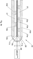
- Fig. 3a provides a perspective view of a button assembly 30 according to an embodiment of the present invention.
- Fig. 3b provides a cross sectional view of the button assembly 30, illustrated in a configuration in which no electrical signal is being generated.
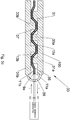
- Fig. 3c provides a cross sectional view of the button assembly 30, illustrated in a configuration in which an electrical signal is generated.
- the button assembly 30 comprises, a first element 31a having a plurality of nodules 33a and a second element 31b having a plurality of nodules 33b.
- the first and second elements 31a,31b are arranged to overlay one another and the nodules 33a of the first element 31a extend in a direction towards the second element 31b, and the nodules 33b of the second element 31b extend in a direction towards the first element 31a.
- the first and second elements 31a,b are arranged such that the nodules 33a,33b of the first and second elements 31a,31b are offset from one another such that moving one of the elements 31a,31b towards the other 31a,31b will cause the nodules 33a,33b of one element 31a,31b to be received between the nodules 33a,33b of the other element 31a,31b; in other words moving one of the elements 31a,31b towards the other 31a,31b will cause the nodules 33a,33b of one element 31a,31b to be received into spaces 37 which are between nodules 33a,33b of the other element 31a,31b.
- the button assembly 30 further comprises a flexible film 35 comprising piezoelectric material.
- the flexible film 35 is arranged to be interposed between the first and second elements 31a,31b.
- the flexible film 35 is arranged to be interposed between the first and second elements 31a,31b so that the nodules 33a,33b of both the first and second elements 31a,31b extend in a direction towards the flexible film 35.
- the flexible film 35 comprises a core 9a which comprises piezoelectric material.
- the core 9a will be both flexible and elastic.
- the core 9a is composed of a silicone substrate having dipole particles (preferably micor or nano dipole particles) embedded therein (the silicone substrate is both flexible and elastic.
- the dipolar particles may comprise organic and/or inorganic material.
- the dipolar particles comprise polymer; specifically, the dipolar particles comprise copolymers which comprise acrylonitrile and/or methacrylates. These provide for highly polar dipolar particles.
- the dipole of the dipolar particles can be enhanced by, for example, poling of the material with a strong electric field at a temperature higher than the glass transmission temperature of the particles. The poling remains after cooling of the dipolar particles below the glass transmission temperature.
- the dipolar particles comprise polymer inorganic materials; for example, the dipolar particles which comprise BaTiO3.
- the flexible film 35 further comprises a first flexible electrically conductive coating 11a, provided on a first surface 13a of the core 9a, which defines a first electrode 11a, and a second flexible electrically conductive costing 11b, provided on a second, opposite, surface 13b of the core 9a, which defines a second electrode 11b.
- the first and second electrodes 11a,11b are electrically isolated from one another; in this example this is achieved by ensuring that the first flexible electrically conductive coating 11a and second flexible electrically conductive coating 11b are independent of one another by provided them on opposite surfaces 13a,13b of the core 9a of the flexible film 35.
- the first flexible electrically conductive coating 11a comprises at least one of: carbon particles such as Carbon Black, Graphene, Fullerenes, Nanotubes; and/or metallic particles such as flakes and/or nanowires of Silver, Gold, Tungsten and/or Nickel; and/or semiconducting particles such as Silicon, Indiumphosphid and Galliumnitride particles; and/or conductive polymers such as Poly-3,4-ethylendioxythiophen (PEDOT, PEDT), Polyethin(or Polyacetylen, PAC), Polyanilin (PAni), Polyparaphenylen (PPP), Polythiophen (PT) and/or Polypyrrol (PPy).
- carbon particles such as Carbon Black, Graphene, Fullerenes, Nanotubes
- metallic particles such as flakes and/or nanowires of Silver, Gold, Tungsten and/or Nickel
- semiconducting particles such as Silicon, Indiumphosphid and Galliumnitride particles
- the electrically conductive material may comprise conductive fibres and/or a conductive cloth, which may comprise metal and/or conductive polymer(s).
- the second flexible electrically conductive coating 11b comprises at least one of: carbon particles such as Carbon Black, Graphene, Fullerenes, Nanotubes; and/or metallic particles such as flakes and/or nanowires of Silver, Gold, Tungsten and/or Nickel; and/or semiconducting particles such as Silicon, Indiumphosphid and Galliumnitride particles; and/or conductive polymers such as Poly-3,4-ethylendioxythiophen (PEDOT, PEDT), Polyethin(or Polyacetylen, PAC), Polyanilin (PAni), Polyparaphenylen (PPP), Polythiophen (PT) and/or Polypyrrol (PPy).
- the electrically conductive material may comprise conductive fibres and/or a conductive cloth, which may comprise metal and/or conductive polymer(s).
- the flexible film 35 may further comprise a protective layer 15 which is provided on the first flexible electrically conductive coating 11a, and a protective layer 15 which is provided on the second flexible electrically conductive coating 11b.
- Each protective layer 15 may comprise of flexible materials such as Polyurethane, natural and/or synthetic rubber, Silicone, Polyacrylate. It should be noted that the assembly 30 shown in Figs. 3a - 3c , does not comprise any protective layer 15.
- moving one of the elements 31a,31b towards the other 31a,31b will cause the nodules 33a,33b of one element 31a,31b to be received between the nodules 33a,33b of the other element 31a,31b; in other words moving one of the elements 31a,31b towards the other 31a,31b will cause the nodules 33a,33b of one element 31a,31b to be received into spaces 37 which are between nodules 33a,33b of the other element 31a,31b.
- the flexible film 35 Since the flexible film 35 is arranged to be interposed between the first and second elements 31a,31b, the flexible film 35 will be stretched as nodules 33a,33b of one element 31a,31b to be received between the nodules 33a,33b of the other element 31a,31b.
- the piezoelectric material in the flexible film 35 is defined by the dipolar particles provided in the core 9a; due to the composition of the core 9a containing dipolar particles, this makes the core piezoelectric, and thus makes the flexible film 35 piezoelectric. Accordingly, the stretching of the flexible film 35 will generate an electrical signal.
- Fig. 3c illustrates the button assembly 30 after one of the elements 31a,31b towards the other 31a,31b to cause the nodules 33a,33b of one element 31a,31b to be received between the nodules 33a,33b of the other element 31a,31b; in other words one of the elements 31a,31b has been moved towards the other 31a,31b to cause the nodules 33a,33b of one element 31a,31b to be received into spaces 37 which are between nodules 33a,33b of the other element 31a,31b, thereby stretching the flexible film 35 to generate an electrical signal.
- the film When the film is stretched its thickness is reduced; the reduction in the thickness reduces the distance between dipolar particles in the film, and hence the density of the dipolar particles which is between the first and second electrodes is increased.
- the increase of the density of dipolar particles between the first and second electrodes increases the total polarization of the film between the first and the second electrodes. This increase of total polarization induces an electric charge which is collected by the first and second electrodes.
- the electric charge which is collected by the first and second electrodes can be converted into a voltage signal using, for example, discrete electronic components. The voltage can then be fed to a digital interface such as USB, CAN, LIN or KNX.
- the flexible film 35 will generate an electric charge due to the mechanical stress of stretching; this generated electric charge will pass to the first and second flexible electrically conductive coatings 11a,11b thereby generating an electrical charge which can be collected and converted into a voltage signal.
- Advantageously stretching of the flexible film 35 creates more mechanical stress in the core 9a compared to the mechanical stress created by just compression of the flexible film 35; accordingly compared to prior art solutions a much stronger electrical signal is generated.
- the flexible film 35 will be compressed between each element 31a,31b and the nodules 33a,33b of the other element 31a,31b.
- This compression of the flexible film 35 will further increase the mechanical stress in the flexible film (in particular will further increase the mechanical stress in the core 9a of the flexible film 35) which causes a further increase in the density of the dipolar particles which is between the first and second electrodes, which in turn increase in the electrical signal which is generated.
- first and second elements 31a,31b may take any suitable design, shape or configuration.
- the first and second elements 31a,31b are mechanically connected via a flexible connecting portion 39.
- the first and second elements 31a,31b are mechanically independent.
- the assembly 30, comprises a single flexible strip 100 comprising a first region 31a having a plurality of nodules 33a, wherein the first region 31a defines said first element 31a, and a second region 31b having a plurality of nodules 33b, wherein the second region 31b defines said second element 31b; and wherein the flexible strip 100 further comprises a flexible connecting portion 39 which connects the first and second regions 31a,31b.
- the single flexible strip 100 is folded at the flexible connecting portion 39 so that, the first and second regions 31a,31b overlay one another and the nodules 33a of the first region 31a extend in a direction towards the second region 31b, and the nodules 31b of the second region 31b extend in a direction towards the first region 31a, and so that the nodules 33a of the first region 31a are offset from the nodules 33b of the second region 31b.
- the flexible film 35 is sandwiched between the first and second regions 31a,31b; in particular the flexible film 35 is sandwiched between the nodules 33a,33b of the first and second regions 31a,31b.
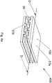
- Figure 5 provides a perspective view of the single flexible strip 100 which is provided in the assembly 30 of Figs. 3a - 3c .
- the a flexible strip is not essential to the present invention; for example the first and second elements 31a,31b may be mechanically independent elements.
- the strip 100 comprises a first region 31a having a plurality of nodules 33a and a second region 31b having a plurality of nodules 33b.
- the first and second regions 31a,31b define the first and second elements 31a,31b respectively.
- the nodules 33a,33b may have any suitable profile; in this example the nodules 33a,33b are cylindrical shaped. Also in this example the nodules 33a,33b are substantially rigid; in this embodiment the nodules 33a,33b are configured to each have a Young's modulus of 20N/mm 2 .
- the nodules 33a,33b may be configured to have a Young's modulus of any value, however preferably the nodules 33a,33b are configured to have a Young's modulus of between 1-100 N/mm 2 , preferably 0.3-30N/mm 2 .
- a flexible connecting portion 39 is interposed between the first and second regions 31a,31b.
- the flexible connecting portion 39 connects the first and second regions 31a,31b.
- the flexible connecting portion 39 is designed such as to allow the strip 100 to be folded at this section so that the first and second regions 31a,31b can be moved to overlay one another.
- an axis 108 which is parallel to the plane of the strip 100, and which extends across the flexible connecting portion 39, defines a fold line 108 along which the strip 100 is to be folded.
- the axis 108 will be positioned to bisect the length of the flexible connecting portion 39.
- the first and second regions 31a,31b the nodules 33a,33b and the flexible connecting portion 39 all have the same material composition.
- the thickness (in a direction perpendicular to the plane of the strip 100) of flexible connecting portion 39 is less than the thickness (in a direction perpendicular to the plane of the strip 1) of the regions of the first and second regions 31a,31b which are without nodules 33a,33b, thus making it easier to fold the strip 100 at the flexible connecting portion 39.
- the strip 100 is formed of a single moulded piece.
- the flexible connecting portion 39 further comprises a cut-out 107 which reduces the amount of material present in the flexible connecting portion 39, which further increases the flexibility of the flexible connecting portion 39.
- the cut-out 107 is an optional feature.
- the material composition of the first and second regions 31a,31b, and nodules 33a,33b is different to the material composition of the flexible connecting portion 39; in such an embodiment the regions of the first and second regions 31a,31b which are without nodules 33a,33b, and the flexible connecting portion 39 may all have equal thicknesses, but the flexible connecting portion 39 may be composed of material which is more flexible than the material of the first and second regions 31a,31b, thus making it easier to fold the strip 100 at the flexible connecting portion 39.
- the strip 100 further comprises at least one alignment window provided on one side of the axis 108 and a corresponding alignment window(s) provided on the opposite side of the axis 108.
- the strip 100 comprises eight alignment windows 109a-d and 110a-d. Alignment windows 109a-d are defined by respective apertures in the flexible connecting portion 39 and alignment windows 110a-d are defined by apertures provided in flaps 111 which extend at opposing end extremities of the strip 100.
- the alignment windows 109a,b, 110a,b are located on one side of the axis 108 and the corresponding alignment windows 109c,d, 110c,d are located on the opposite side of the axis 108. It should be understood that any number of alignment windows may be provided.
- the alignment windows aid correct positioning of the first and second regions 31a,31b with respect to one another when the strip 100 is folded at the flexible connecting portion 39.
- the alignment windows 109a-d and 110a-d are positioned such that when the strip 100 is folded, and the alignment windows 109a,b, 110a,b located on one side of the axis 108 are aligned with the corresponding alignment windows 109c,d, 110c,d located on the opposite side of the axis 108, then the first and second regions 31a,31b will have a predefined position with respect to one another; specifically the first and second regions 31a,31b will overlay one another and the nodule 33a on the first region 31a will be offset from the nodules 33b of the second region 31b.
- alignment windows 109a-d defined by respective apertures in the first and second regions 31a,31b are provided.
- the alignment windows 110a-d defined by apertures provided in flaps 111 at opposing end extremities of the silicone strip 100 are provided.
- the alignment windows 109a-d, 110a-d are optional features; the provision of alignment windows is not essential for the invention.
- no alignment windows are provided.
- the perimeters 112a, 112b of the respective first and second regions 31a,31b are used to aid correct positioning of the first and second regions 31a,31b with respect to one another when the strip 100 is folded:
- first and second regions 31a,31b will have a predefined, desired, position with respect to one another; specifically the first and second regions 31a,31b will overlay one another and the nodule 33a on the first region 31a will be offset from the nodules 33b of the second region 31b.
- the positions of the plurality of nodules 33a in the first region 31a do not correspond to the positions of the plurality of nodules 33b in the second region 31b.
- the positions of the plurality of nodules 33a in the first region 31a are such that when the strip 100 is folded at the flexible connecting portion 39, and the respective alignment windows 109a-d and 110a-d aligned and/or the respective perimeters 112a,112b aligned, the nodules 33a in the first region 31a will be offset from the nodules 33b in the second region 31b.
- the nodules 33a in the first region 31a will have a predefined position with respect to the nodules 33b in the second region 31b.
- each respective nodule 33b of the second region 31b will be positioned above a centre point between four adjacent nodules 33a of the first region 33a; for example the nodule 33a1 in the second region 33b will be positioned above the centre point 106 between the four adjacent nodules 33b1-b4 in the first region 31a.
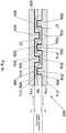
- the flexible electrically conductive coatings are provided on the first and second elements rather than on the flexible film, as shown in Figures 4a - 4c .
- the assembly 400 shown in Figures 4a - 4c has many of the same features as the assembly 30 shown in Figures 3a - 3c and like features are awarded the same reference numbers.
- the first and second elements 31a,31b are provided as mechanically independent elements.
- the first element 31a has a first electrically conductive coating 45a provided its surface 41a which is facing the second element 31b; and a second element 31b has a second electrically conductive coating 45b provided its surface 41b which is facing the first element 31a.
- the first electrically conductive coating 45a defines a first electrode 11a and the second electrically conductive coating 45b defines a second electrode 11b.
- the assembly 400 comprises a film 435 which is without electrically conductive coatings (in other word the film 435 consists a core 9a only).
- the film 435 comprises piezoelectric material.
- the film 435 is composed of a silicone substrate having dipolar particles embedded therein.
- the dipolar particles define the piezoelectric material in the film 435.
- the dipolar particles may comprise organic and/or inorganic material.
- the dipolar particles comprise polymer; specifically, the dipolar particles comprise copolymers which comprise acrylonitrile and/or methacrylates. These provide for highly polar dipolar particles.
- the dipole of the dipolar particles can be enhanced by, for example, poling of the material with a strong electric field at a temperature higher than the glass transmission temperature of the particles. The poling remains after cooling of the dipolar particles below the glass transmission temperature.
- the dipolar particles comprise polymer inorganic materials; for example, the dipolar particles which comprise BaTiO3.
- moving one of the elements 31a,31b towards the other 31a,31b will cause the nodules 33a,33b of one element 31a,31b to be received between the nodules 33a,33b of the other element 31a,31b; in other words moving one of the elements 31a,31b towards the other 31a,31b will cause the nodules 33a,33b of one element 31a,31b to be received into spaces 37 which are between nodules 33a,33b of the other element 31a,31b.
- the flexible film 435 Since the flexible film 435 is arranged to be interposed between the first and second elements 31a,31b, the flexible film 435 will be stretched as nodules 33a,33b of one element 31a,31b to be received between the nodules 33a,33b of the other element 31a,31b. Due to the composition of the film 435 containing piezoelectric material in the form of dipolar particles the stretching of the flexible film 435 will generate an electrical signal.
- Fig. 4b illustrates the button assembly 30 after one of the elements 31a,31b towards the other 31a,31b to cause the nodules 33a,33b of one element 31a,31b to be received between the nodules 33a,33b of the other element 31a,31b; in other words one of the elements 31a,31b has been moved towards the other 31a,31b to cause the nodules 33a,33b of one element 31a,31b to be received into spaces 37 which are between nodules 33a,33b of the other element 31a,31b, thereby stretching the flexible film 435 to generate an electrical signal.
- the film 435 when the film 435 is stretched its thickness is reduced; the reduction in the thickness reduces the distance between dipolar particles in the film 435, and hence the density of the dipolar particles which is between the first electrically conductive coating 45a and the second electrically conductive coating 45b is increased.
- the increase of the density of dipolar particles between the first electrically conductive coating 45a and the second electrically conductive coating 45b increases the total polarization of the film 435 between the first electrically conductive coating 45a and the second electrically conductive coating 45b. This increase of total polarization induces an electric charge which is collected by the first electrically conductive coating 45a and the second electrically conductive coating 45b.
- the electric charge generated by the film 435 will pass from the film 435 into the first electrically conductive coating 45a at the areas 50a where the first electrically conductive coating 45a contacts the film 435.
- the electric charge generated by the film 435 will also pass from the film 435 into the second electrically conductive coating 45b at the areas 50b where the second electrically conductive coating 45b contacts the film 435.
- the electric charge generated by the film 435 will pass to the first and second flexible electrically conductive coatings 11a,11b at the areas 50a,b where the respective first and second electrically conductive coatings 45a,45b contact the film 435.
- the electric charge which is collected can be converted into a voltage signal using, for example, discrete electronic components.
- the voltage can then be fed to a digital interface such as USB, CAN, LIN or KNX.
- the flexible film 435 will generate an electric charge due to the mechanical stress of stretching; this generated electric charge will pass to the first and second flexible electrically conductive coatings 11a,11b thereby generating an electrical charge which can be collected and converted into a voltage signal.
- Advantageously stretching of the flexible film 9 creates more mechanical stress in the core 9a compared to the mechanical stress created by just compression of the flexible film 35; accordingly compared to prior art solutions a much stronger electrical signal is generated.
- the flexible film 435 will be compressed between each element 31a,31b and the nodules 33a,33b of the other element 31a,31b at the areas 50a,b where the respective first and second electrically conductive coatings 45a,45b contact the film 435.
- This compression of the flexible film 435 will further increase the mechanical stress in the flexible film 435 which causes a further increase in the electrical signal which is generated.
Landscapes
- General Electrical Machinery Utilizing Piezoelectricity, Electrostriction Or Magnetostriction (AREA)
- Push-Button Switches (AREA)
Claims (8)
- Knopfanordnung (30, 400), umfassend:ein erstes Element (31a) mit einer Mehrzahl von Knötchen (33a) und ein zweites Element (31b) mit einer Mehrzahl von Knötchen (33b), und wobei das erste und das zweite Element (31a,b) so angeordnet sind, dass sie einander überlagern, und die Knötchen (33a) des ersten Elements sich in einer Richtung zum zweiten Element (31b) erstrecken, und die Knötchen (33b) des zweiten Elements (31b) sich in einer Richtung zum ersten Element (31a) erstrecken, und wobei das erste und das zweite Element (31a,b) derart angeordnet sind, dass die Knötchen (33a) des ersten Elements (31a) von den Knötchen (33b) des zweiten Elements (31b) versetzt sind, und die Knötchen (33b) des zweiten Elements (31b) von den Knötchen (33a) des ersten Elements (31a) versetzt sind, derart dass ein Bewegen eines des ersten und des zweiten Elements (31a, 31b) zum anderen (31a, 31b) bewirkt, dass die Knötchen (33a, 33b) eines des ersten und des zweiten Elements (31a, 31b) zwischen den Knötchen (33a, 33b) des anderen Elements (31a, 31b) aufgenommen werden;einen flexiblen Film (35), der piezoelektrisches Material umfasst;eine erste Elektrode (11a), die sich zwischen dem flexiblen Film und dem ersten Element (31a) befindet, und eine zweite Elektrode (11b), die sich zwischen dem flexiblen Film (35) und dem zweiten Element (31b) befindet;wobei der flexible Film (35) so angeordnet ist, dass er derart zwischen das erste und das zweite Element (31a,b) eingefügt ist, dass ein Bewirken der Aufnahme der Knötchen (33a,b) eines Elements (31a,b) zwischen den Knötchen (33a,b) des anderen Elements (31a,b) durch Bewegen eines des ersten und des zweiten Elements (31a, 31b) zum anderen (31a, 31b) bewirkt, dass der flexible Film (35) gestreckt wird, um dadurch ein elektrisches Signal in der ersten und der zweiten Elektrode (11a,b) zu erzeugen,wobei die Knopfanordnung einen einzigen flexiblen Streifen (35) umfasst, der eine erste Region (31a) mit einer Mehrzahl von Knötchen (33a), wobei die erste Region das erste Element (31a) definiert, und eine zweite Region (31b) mit einer Mehrzahl von Knötchen (33b) umfasst, wobei die zweite Region (31b) das zweite Element (31b) definiert; und wobei der flexible Streifen (35) ferner einen flexiblen Verbindungsabschnitt (39) umfasst, der die erste und die zweite Region (31a,b) verbindet; und wobei der flexible Streifen (100) am flexiblen Verbindungsabschnitt (39) so gefaltet ist, dass die erste und die zweite Region (31a,b) einander überlagern, und die Knötchen (33a) der ersten Region (31a) sich in einer Richtung zur zweiten Region (31b) erstrecken, und die Knötchen (33b) der zweiten Region (31b) sich in einer Richtung zur ersten Region (31b) erstrecken, und so, dass die Knötchen (33a) der ersten Region (31a) von den Knötchen (33b) der zweiten Region (31b) versetzt sind, und die Knötchen (33b) der zweiten Region (31b) von den Knötchen (33a) der ersten Region (31a) versetzt sind, und wobei der flexible Film (35) sandwichartig zwischen die erste und die zweite Region (31a,b) des gefalteten flexiblen Streifens (100) eingefügt ist.
- Knopfanordnung nach Anspruch 1, wobei der flexible Film ferner eine erste flexible elektrisch leitende Beschichtung, die auf einer Oberfläche des Films vorgesehen ist, welche die erste Elektrode definiert, und eine zweite flexible elektrisch leitende Beschichtung umfasst, die auf einer zweiten, gegenüberliegenden Oberfläche des Films vorgesehen ist, welche die zweite Elektrode definiert.
- Knopfanordnung nach Anspruch 1, wobei das erste Element eine erste elektrisch leitende Beschichtung aufweist, die auf einer Oberfläche vorgesehen ist, die dem zweiten Element gegenüberliegt und die erste Elektrode definiert, und das zweite Element eine zweite elektrisch leitende Beschichtung aufweist, die auf einer Oberfläche vorgesehen ist, die dem ersten Element gegenüberliegt und die zweite Elektrode definiert.
- Knopfanordnung nach Anspruch 2 oder 3, wobei der flexible Film einen Kern umfasst, der elastomeres Material umfasst; und wobei das piezoelektrische Material zweipolige Teilchen umfasst, die in den Kern eingebettet sind.
- Knopfanordnung nach einem der Ansprüche 2 bis 4, wobei der Film ferner eine Schutzschicht, die auf der ersten flexiblen elektrisch leitenden Beschichtung vorgesehen ist, und eine Schutzschicht umfasst, die auf der zweiten flexiblen elektrisch leitenden Beschichtung vorgesehen ist.
- Knopfanordnung nach Anspruch 5, wobei die Schutzschicht Polyurethan, Natur- und/oder Kunstkautschuk, Silikon und/oder Polyacrylat umfasst.
- Knopfanordnung nach Anspruch 2, wobei
die erste flexible elektrisch leitende Beschichtung mindestens eines umfasst von: Kohlenstoffteilchen, wie beispielsweise Ruß, Graphen, Fullerenen, Nanoröhrchen; und/oder Metallteilchen, wie beispielsweise Flocken und/oder Nanodrähten von Silber, Gold, Wolfram und/oder Nickel; und/oder Halbleiterteilchen, wie beispielsweise Silicium-, lndiumphosphid- und Galliumnitrid-Teilchen; und/oder leitenden Polymeren, wie beispielsweise Poly-3,4-ethylendioxythiophen, PEDOT, PEDT, Polyethin oder Polyacetylen, PAC, Polyanilin, PAni, Polyparaphenylen, PPP, Polythiophen, PT, und/oder Polypyrrol, PPy; und
die zweite flexible elektrisch leitende Beschichtung mindestens eines umfasst von: Kohlenstoffteilchen, wie beispielsweise Ruß, Graphen, Fullerenen, Nanoröhrchen; und/oder Metallteilchen, wie beispielsweise Flocken und/oder Nanodrähten von Silber, Gold, Wolfram und/oder Nickel; und/oder Halbleiterteilchen, wie beispielsweise Silicium-, lndiumphosphid- und Galliumnitrid-Teilchen; und/oder leitenden Polymeren, wie beispielsweise Poly-3,4-ethylendioxythiophen, PEDOT, PEDT, Polyethin oder Polyacetylen, PAC, Polyanilin, PAni, Polyparaphenylen, PPP, Polythiophen, PT, und/oder Polypyrrol, PPy. - Verfahren von Herstellung einer Knopfanordnung (30, 400), umfassend:Bereitstellen eines ersten Elements (31a) mit einer Mehrzahl von Knötchen (33a) und eines zweiten Elements (31b) mit einer Mehrzahl von Knötchen (33b);derartiges Anordnen des ersten und des zweiten Elements (31a,b), dass sie einander überlagern, derart dass die Knötchen (33a) des ersten Elements (31a) sich in einer Richtung zum zweiten Element (31b) erstecken, und die Knötchen (33b) des zweiten Elements (31b) sich in einer Richtung zum ersten Element (31a) erstrecken, und derart, dass die Knötchen (33a) des ersten Elements (31a) von den Knötchen (33b) des zweiten Elements (31b) versetzt sind, und die Knötchen (33b) des zweiten Elements (31b) von den Knötchen (33a) des ersten Elements (31a) versetzt sind, derart dass ein Bewegen eines des ersten und des zweiten Elements (31a, 31b) zum anderen (31a, 31b) bewirkt, dass die Knötchen (33a, 33b) eines des ersten und des zweiten Elements (31a, 31b) zwischen den Knötchen (33a, 33b) des anderen Elements (31a, 31b) aufgenommen werden;Bereitstellen eines flexiblen Films (35), der piezoelektrisches Material umfasst;Bereitstellen einer ersten Elektrode (11a) zwischen dem flexiblen Film (35) und dem ersten Element (11a) und einer zweiten Elektrode (11b) zwischen dem flexiblen Film (35) und dem zweiten Element (11b);derartiges Anordnen des flexiblen Films (35), dass er zwischen das erste und das zweite Element (31a,b) eingefügt wird, derart dass ein Bewirken der Aufnahme der Knötchen (33a,b) eines Elements (31a,b) zwischen den Knötchen (33a,b) des anderen Elements (31a,b) durch Bewegen eines des ersten und des zweiten Elements (31a, 31b) zum anderen (31a, 31b) bewirkt, dass der flexible Film (35) gestreckt wird, um dadurch ein elektrisches Signal in der ersten und der zweiten Elektrode zu erzeugen,wobei der Schritt des derartigen Anordnens des ersten und des zweiten Elements, dass sie einander überlagern, ein Falten eines einzigen flexiblen Streifens (100) umfasst, der eine erste Region (31a) mit einer Mehrzahl von Knötchen (33a), wobei die erste Region das erste Element (31a) definiert, und eine zweite Region (31b) mit einer zweiten Mehrzahl von Knötchen (33b), wobei die zweite Region (31b) das zweite Element (31b) definiert, und einen flexiblen Verbindungsabschnitt (39) umfasst, der das erste und das zweite Element (33a,b) so verbindet, dass der flexible Film (35) sandwichartig zwischen die erste und die zweite Region (31a,b) des gefalteten flexiblen Streifens (100) eingefügt wird.
Applications Claiming Priority (2)
| Application Number | Priority Date | Filing Date | Title |
|---|---|---|---|
| CH15882016 | 2016-12-05 | ||
| PCT/IB2017/056365 WO2018104807A1 (en) | 2016-12-05 | 2017-10-13 | Button assemblies |
Publications (2)
| Publication Number | Publication Date |
|---|---|
| EP3549262A1 EP3549262A1 (de) | 2019-10-09 |
| EP3549262B1 true EP3549262B1 (de) | 2021-04-07 |
Family
ID=60382482
Family Applications (1)
| Application Number | Title | Priority Date | Filing Date |
|---|---|---|---|
| EP17800603.7A Active EP3549262B1 (de) | 2016-12-05 | 2017-10-13 | Knopfanordnungen |
Country Status (3)
| Country | Link |
|---|---|
| US (1) | US11025251B2 (de) |
| EP (1) | EP3549262B1 (de) |
| WO (1) | WO2018104807A1 (de) |
Families Citing this family (6)
| Publication number | Priority date | Publication date | Assignee | Title |
|---|---|---|---|---|
| US11340123B2 (en) * | 2019-08-12 | 2022-05-24 | Parker-Hannifin Corporation | Electroactive polymer pressure sensor having corrugating capacitor |
| JP7264136B2 (ja) * | 2020-08-28 | 2023-04-25 | 横河電機株式会社 | 力検出装置、力検出システム及び力検出装置の製造方法 |
| CN112532106A (zh) * | 2020-10-30 | 2021-03-19 | 武汉汉烯科技有限公司 | 基于宏观石墨烯膜负泊松比结构的柔性压电能量收集器 |
| JP7558054B2 (ja) * | 2020-12-24 | 2024-09-30 | 横河電機株式会社 | 力検出器及び力検出システム |
| CN113068961B (zh) * | 2021-03-09 | 2023-06-13 | 青岛大学 | 一种基于柔性传感器的床垫 |
| WO2022250939A1 (en) * | 2021-05-27 | 2022-12-01 | The University Of Chicago | Strain-insensitive soft pressure sensor and method of measuring pressure |
Family Cites Families (3)
| Publication number | Priority date | Publication date | Assignee | Title |
|---|---|---|---|---|
| JPS5643551U (de) | 1979-09-13 | 1981-04-20 | ||
| FR2581496B1 (fr) * | 1985-05-02 | 1987-06-26 | Silec Liaisons Elec | Capteur microphonique de contact a membrane piezo polymere |
| JPH0935570A (ja) | 1995-07-21 | 1997-02-07 | Yazaki Corp | スイッチ装置 |
-
2017
- 2017-10-13 EP EP17800603.7A patent/EP3549262B1/de active Active
- 2017-10-13 WO PCT/IB2017/056365 patent/WO2018104807A1/en not_active Ceased
- 2017-10-13 US US16/337,151 patent/US11025251B2/en active Active
Non-Patent Citations (1)
| Title |
|---|
| None * |
Also Published As
| Publication number | Publication date |
|---|---|
| WO2018104807A1 (en) | 2018-06-14 |
| US20190229728A1 (en) | 2019-07-25 |
| US11025251B2 (en) | 2021-06-01 |
| EP3549262A1 (de) | 2019-10-09 |
Similar Documents
| Publication | Publication Date | Title |
|---|---|---|
| US11025251B2 (en) | Button assemblies | |
| CN100530931C (zh) | 弹性体致动器及制造致动器的方法 | |
| Pelrine et al. | High-field deformation of elastomeric dielectrics for actuators | |
| EP3504725B1 (de) | Flexible kondensatoren und verfahren zur herstellung der flexiblen kondensatoren | |
| US8785914B2 (en) | Piezoelectric nanowire structure and electronic device including the same | |
| CN105826283A (zh) | 电子设备 | |
| KR20140072027A (ko) | 압전형 압력 센서 | |
| WO2012108192A1 (ja) | 静電容量変化型発電素子 | |
| US20190306972A1 (en) | Electric element and electronic device | |
| KR20170126302A (ko) | 압력 센서 소자 및 압력 센서 소자 제조 방법 | |
| CN106575583A (zh) | 触摸式输入装置和电子设备 | |
| MX2008001195A (es) | Conmutadores y sensores interdigitales de fuerza. | |
| KR101582991B1 (ko) | 플렉서블 유기박막 트랜지스터 및 이를 포함한 센서 | |
| US20140042392A1 (en) | Double contacts for carbon nanotubes thin film devices | |
| WO2018207707A1 (ja) | アクチュエータ、駆動部材、触覚提示装置および駆動装置 | |
| US20220294366A1 (en) | Actuator | |
| JP5674222B2 (ja) | 積層型静電アクチュエータ | |
| KR20180103051A (ko) | 변환기 | |
| US11888412B2 (en) | Stackable actuating element with profiled insulated electrode structures | |
| US20200287478A1 (en) | Actuator | |
| JP6806328B2 (ja) | 電子装置 | |
| JP2021518635A (ja) | 可撓性スイッチ、センサーおよび回路 | |
| KR102417498B1 (ko) | 압력 감지 센서 및 이를 포함하는 압력 감지 인솔 | |
| US7476819B1 (en) | Switch box for multi-directional activation of a ribbon switch | |
| CN107665851B (zh) | 元件选取系统 |
Legal Events
| Date | Code | Title | Description |
|---|---|---|---|
| STAA | Information on the status of an ep patent application or granted ep patent |
Free format text: STATUS: UNKNOWN |
|
| STAA | Information on the status of an ep patent application or granted ep patent |
Free format text: STATUS: THE INTERNATIONAL PUBLICATION HAS BEEN MADE |
|
| PUAI | Public reference made under article 153(3) epc to a published international application that has entered the european phase |
Free format text: ORIGINAL CODE: 0009012 |
|
| STAA | Information on the status of an ep patent application or granted ep patent |
Free format text: STATUS: REQUEST FOR EXAMINATION WAS MADE |
|
| 17P | Request for examination filed |
Effective date: 20190418 |
|
| AK | Designated contracting states |
Kind code of ref document: A1 Designated state(s): AL AT BE BG CH CY CZ DE DK EE ES FI FR GB GR HR HU IE IS IT LI LT LU LV MC MK MT NL NO PL PT RO RS SE SI SK SM TR |
|
| AX | Request for extension of the european patent |
Extension state: BA ME |
|
| DAV | Request for validation of the european patent (deleted) | ||
| DAX | Request for extension of the european patent (deleted) | ||
| GRAP | Despatch of communication of intention to grant a patent |
Free format text: ORIGINAL CODE: EPIDOSNIGR1 |
|
| STAA | Information on the status of an ep patent application or granted ep patent |
Free format text: STATUS: GRANT OF PATENT IS INTENDED |
|
| INTG | Intention to grant announced |
Effective date: 20201215 |
|
| GRAS | Grant fee paid |
Free format text: ORIGINAL CODE: EPIDOSNIGR3 |
|
| GRAA | (expected) grant |
Free format text: ORIGINAL CODE: 0009210 |
|
| STAA | Information on the status of an ep patent application or granted ep patent |
Free format text: STATUS: THE PATENT HAS BEEN GRANTED |
|
| AK | Designated contracting states |
Kind code of ref document: B1 Designated state(s): AL AT BE BG CH CY CZ DE DK EE ES FI FR GB GR HR HU IE IS IT LI LT LU LV MC MK MT NL NO PL PT RO RS SE SI SK SM TR |
|
| REG | Reference to a national code |
Ref country code: GB Ref legal event code: FG4D |
|
| REG | Reference to a national code |
Ref country code: AT Ref legal event code: REF Ref document number: 1381000 Country of ref document: AT Kind code of ref document: T Effective date: 20210415 Ref country code: CH Ref legal event code: NV Representative=s name: P&TS SA, CH Ref country code: CH Ref legal event code: EP |
|
| REG | Reference to a national code |
Ref country code: DE Ref legal event code: R096 Ref document number: 602017036336 Country of ref document: DE |
|
| REG | Reference to a national code |
Ref country code: IE Ref legal event code: FG4D |
|
| REG | Reference to a national code |
Ref country code: LT Ref legal event code: MG9D |
|
| REG | Reference to a national code |
Ref country code: NL Ref legal event code: MP Effective date: 20210407 Ref country code: AT Ref legal event code: MK05 Ref document number: 1381000 Country of ref document: AT Kind code of ref document: T Effective date: 20210407 |
|
| PG25 | Lapsed in a contracting state [announced via postgrant information from national office to epo] |
Ref country code: HR Free format text: LAPSE BECAUSE OF FAILURE TO SUBMIT A TRANSLATION OF THE DESCRIPTION OR TO PAY THE FEE WITHIN THE PRESCRIBED TIME-LIMIT Effective date: 20210407 Ref country code: AT Free format text: LAPSE BECAUSE OF FAILURE TO SUBMIT A TRANSLATION OF THE DESCRIPTION OR TO PAY THE FEE WITHIN THE PRESCRIBED TIME-LIMIT Effective date: 20210407 Ref country code: BG Free format text: LAPSE BECAUSE OF FAILURE TO SUBMIT A TRANSLATION OF THE DESCRIPTION OR TO PAY THE FEE WITHIN THE PRESCRIBED TIME-LIMIT Effective date: 20210707 Ref country code: NL Free format text: LAPSE BECAUSE OF FAILURE TO SUBMIT A TRANSLATION OF THE DESCRIPTION OR TO PAY THE FEE WITHIN THE PRESCRIBED TIME-LIMIT Effective date: 20210407 Ref country code: FI Free format text: LAPSE BECAUSE OF FAILURE TO SUBMIT A TRANSLATION OF THE DESCRIPTION OR TO PAY THE FEE WITHIN THE PRESCRIBED TIME-LIMIT Effective date: 20210407 Ref country code: LT Free format text: LAPSE BECAUSE OF FAILURE TO SUBMIT A TRANSLATION OF THE DESCRIPTION OR TO PAY THE FEE WITHIN THE PRESCRIBED TIME-LIMIT Effective date: 20210407 |
|
| PG25 | Lapsed in a contracting state [announced via postgrant information from national office to epo] |
Ref country code: GR Free format text: LAPSE BECAUSE OF FAILURE TO SUBMIT A TRANSLATION OF THE DESCRIPTION OR TO PAY THE FEE WITHIN THE PRESCRIBED TIME-LIMIT Effective date: 20210708 Ref country code: IS Free format text: LAPSE BECAUSE OF FAILURE TO SUBMIT A TRANSLATION OF THE DESCRIPTION OR TO PAY THE FEE WITHIN THE PRESCRIBED TIME-LIMIT Effective date: 20210807 Ref country code: RS Free format text: LAPSE BECAUSE OF FAILURE TO SUBMIT A TRANSLATION OF THE DESCRIPTION OR TO PAY THE FEE WITHIN THE PRESCRIBED TIME-LIMIT Effective date: 20210407 Ref country code: SE Free format text: LAPSE BECAUSE OF FAILURE TO SUBMIT A TRANSLATION OF THE DESCRIPTION OR TO PAY THE FEE WITHIN THE PRESCRIBED TIME-LIMIT Effective date: 20210407 Ref country code: NO Free format text: LAPSE BECAUSE OF FAILURE TO SUBMIT A TRANSLATION OF THE DESCRIPTION OR TO PAY THE FEE WITHIN THE PRESCRIBED TIME-LIMIT Effective date: 20210707 Ref country code: LV Free format text: LAPSE BECAUSE OF FAILURE TO SUBMIT A TRANSLATION OF THE DESCRIPTION OR TO PAY THE FEE WITHIN THE PRESCRIBED TIME-LIMIT Effective date: 20210407 Ref country code: PL Free format text: LAPSE BECAUSE OF FAILURE TO SUBMIT A TRANSLATION OF THE DESCRIPTION OR TO PAY THE FEE WITHIN THE PRESCRIBED TIME-LIMIT Effective date: 20210407 Ref country code: PT Free format text: LAPSE BECAUSE OF FAILURE TO SUBMIT A TRANSLATION OF THE DESCRIPTION OR TO PAY THE FEE WITHIN THE PRESCRIBED TIME-LIMIT Effective date: 20210809 |
|
| REG | Reference to a national code |
Ref country code: DE Ref legal event code: R097 Ref document number: 602017036336 Country of ref document: DE |
|
| PG25 | Lapsed in a contracting state [announced via postgrant information from national office to epo] |
Ref country code: RO Free format text: LAPSE BECAUSE OF FAILURE TO SUBMIT A TRANSLATION OF THE DESCRIPTION OR TO PAY THE FEE WITHIN THE PRESCRIBED TIME-LIMIT Effective date: 20210407 Ref country code: EE Free format text: LAPSE BECAUSE OF FAILURE TO SUBMIT A TRANSLATION OF THE DESCRIPTION OR TO PAY THE FEE WITHIN THE PRESCRIBED TIME-LIMIT Effective date: 20210407 Ref country code: CZ Free format text: LAPSE BECAUSE OF FAILURE TO SUBMIT A TRANSLATION OF THE DESCRIPTION OR TO PAY THE FEE WITHIN THE PRESCRIBED TIME-LIMIT Effective date: 20210407 Ref country code: DK Free format text: LAPSE BECAUSE OF FAILURE TO SUBMIT A TRANSLATION OF THE DESCRIPTION OR TO PAY THE FEE WITHIN THE PRESCRIBED TIME-LIMIT Effective date: 20210407 Ref country code: SM Free format text: LAPSE BECAUSE OF FAILURE TO SUBMIT A TRANSLATION OF THE DESCRIPTION OR TO PAY THE FEE WITHIN THE PRESCRIBED TIME-LIMIT Effective date: 20210407 Ref country code: SK Free format text: LAPSE BECAUSE OF FAILURE TO SUBMIT A TRANSLATION OF THE DESCRIPTION OR TO PAY THE FEE WITHIN THE PRESCRIBED TIME-LIMIT Effective date: 20210407 Ref country code: ES Free format text: LAPSE BECAUSE OF FAILURE TO SUBMIT A TRANSLATION OF THE DESCRIPTION OR TO PAY THE FEE WITHIN THE PRESCRIBED TIME-LIMIT Effective date: 20210407 |
|
| PLBE | No opposition filed within time limit |
Free format text: ORIGINAL CODE: 0009261 |
|
| STAA | Information on the status of an ep patent application or granted ep patent |
Free format text: STATUS: NO OPPOSITION FILED WITHIN TIME LIMIT |
|
| 26N | No opposition filed |
Effective date: 20220110 |
|
| PG25 | Lapsed in a contracting state [announced via postgrant information from national office to epo] |
Ref country code: IS Free format text: LAPSE BECAUSE OF FAILURE TO SUBMIT A TRANSLATION OF THE DESCRIPTION OR TO PAY THE FEE WITHIN THE PRESCRIBED TIME-LIMIT Effective date: 20210807 Ref country code: AL Free format text: LAPSE BECAUSE OF FAILURE TO SUBMIT A TRANSLATION OF THE DESCRIPTION OR TO PAY THE FEE WITHIN THE PRESCRIBED TIME-LIMIT Effective date: 20210407 |
|
| REG | Reference to a national code |
Ref country code: BE Ref legal event code: MM Effective date: 20211031 |
|
| PG25 | Lapsed in a contracting state [announced via postgrant information from national office to epo] |
Ref country code: MC Free format text: LAPSE BECAUSE OF FAILURE TO SUBMIT A TRANSLATION OF THE DESCRIPTION OR TO PAY THE FEE WITHIN THE PRESCRIBED TIME-LIMIT Effective date: 20210407 |
|
| PG25 | Lapsed in a contracting state [announced via postgrant information from national office to epo] |
Ref country code: LU Free format text: LAPSE BECAUSE OF NON-PAYMENT OF DUE FEES Effective date: 20211013 Ref country code: IT Free format text: LAPSE BECAUSE OF FAILURE TO SUBMIT A TRANSLATION OF THE DESCRIPTION OR TO PAY THE FEE WITHIN THE PRESCRIBED TIME-LIMIT Effective date: 20210407 Ref country code: BE Free format text: LAPSE BECAUSE OF NON-PAYMENT OF DUE FEES Effective date: 20211031 |
|
| PG25 | Lapsed in a contracting state [announced via postgrant information from national office to epo] |
Ref country code: IE Free format text: LAPSE BECAUSE OF NON-PAYMENT OF DUE FEES Effective date: 20211013 |
|
| PG25 | Lapsed in a contracting state [announced via postgrant information from national office to epo] |
Ref country code: CY Free format text: LAPSE BECAUSE OF FAILURE TO SUBMIT A TRANSLATION OF THE DESCRIPTION OR TO PAY THE FEE WITHIN THE PRESCRIBED TIME-LIMIT Effective date: 20210407 |
|
| PG25 | Lapsed in a contracting state [announced via postgrant information from national office to epo] |
Ref country code: HU Free format text: LAPSE BECAUSE OF FAILURE TO SUBMIT A TRANSLATION OF THE DESCRIPTION OR TO PAY THE FEE WITHIN THE PRESCRIBED TIME-LIMIT; INVALID AB INITIO Effective date: 20171013 |
|
| PG25 | Lapsed in a contracting state [announced via postgrant information from national office to epo] |
Ref country code: MK Free format text: LAPSE BECAUSE OF FAILURE TO SUBMIT A TRANSLATION OF THE DESCRIPTION OR TO PAY THE FEE WITHIN THE PRESCRIBED TIME-LIMIT Effective date: 20210407 |
|
| PG25 | Lapsed in a contracting state [announced via postgrant information from national office to epo] |
Ref country code: MT Free format text: LAPSE BECAUSE OF FAILURE TO SUBMIT A TRANSLATION OF THE DESCRIPTION OR TO PAY THE FEE WITHIN THE PRESCRIBED TIME-LIMIT Effective date: 20210407 |
|
| REG | Reference to a national code |
Ref country code: CH Ref legal event code: U11 Free format text: ST27 STATUS EVENT CODE: U-0-0-U10-U11 (AS PROVIDED BY THE NATIONAL OFFICE) Effective date: 20251101 |
|
| PG25 | Lapsed in a contracting state [announced via postgrant information from national office to epo] |
Ref country code: TR Free format text: LAPSE BECAUSE OF FAILURE TO SUBMIT A TRANSLATION OF THE DESCRIPTION OR TO PAY THE FEE WITHIN THE PRESCRIBED TIME-LIMIT Effective date: 20210407 |
|
| PGFP | Annual fee paid to national office [announced via postgrant information from national office to epo] |
Ref country code: DE Payment date: 20251021 Year of fee payment: 9 |
|
| PGFP | Annual fee paid to national office [announced via postgrant information from national office to epo] |
Ref country code: GB Payment date: 20251022 Year of fee payment: 9 |
|
| PGFP | Annual fee paid to national office [announced via postgrant information from national office to epo] |
Ref country code: FR Payment date: 20251030 Year of fee payment: 9 |
|
| PGFP | Annual fee paid to national office [announced via postgrant information from national office to epo] |
Ref country code: CH Payment date: 20251101 Year of fee payment: 9 |