EP3548966B1 - Laminierte elektrooptische anzeigen und verfahren zur herstellung davon - Google Patents
Laminierte elektrooptische anzeigen und verfahren zur herstellung davon Download PDFInfo
- Publication number
- EP3548966B1 EP3548966B1 EP17875756.3A EP17875756A EP3548966B1 EP 3548966 B1 EP3548966 B1 EP 3548966B1 EP 17875756 A EP17875756 A EP 17875756A EP 3548966 B1 EP3548966 B1 EP 3548966B1
- Authority
- EP
- European Patent Office
- Prior art keywords
- substrate
- electro
- backplane
- layer
- conductive layer
- Prior art date
- Legal status (The legal status is an assumption and is not a legal conclusion. Google has not performed a legal analysis and makes no representation as to the accuracy of the status listed.)
- Active
Links
Images


Classifications
-
- G—PHYSICS
- G02—OPTICS
- G02F—OPTICAL DEVICES OR ARRANGEMENTS FOR THE CONTROL OF LIGHT BY MODIFICATION OF THE OPTICAL PROPERTIES OF THE MEDIA OF THE ELEMENTS INVOLVED THEREIN; NON-LINEAR OPTICS; FREQUENCY-CHANGING OF LIGHT; OPTICAL LOGIC ELEMENTS; OPTICAL ANALOGUE/DIGITAL CONVERTERS
- G02F1/00—Devices or arrangements for the control of the intensity, colour, phase, polarisation or direction of light arriving from an independent light source, e.g. switching, gating or modulating; Non-linear optics
- G02F1/01—Devices or arrangements for the control of the intensity, colour, phase, polarisation or direction of light arriving from an independent light source, e.g. switching, gating or modulating; Non-linear optics for the control of the intensity, phase, polarisation or colour
- G02F1/165—Devices or arrangements for the control of the intensity, colour, phase, polarisation or direction of light arriving from an independent light source, e.g. switching, gating or modulating; Non-linear optics for the control of the intensity, phase, polarisation or colour based on translational movement of particles in a fluid under the influence of an applied field
- G02F1/166—Devices or arrangements for the control of the intensity, colour, phase, polarisation or direction of light arriving from an independent light source, e.g. switching, gating or modulating; Non-linear optics for the control of the intensity, phase, polarisation or colour based on translational movement of particles in a fluid under the influence of an applied field characterised by the electro-optical or magneto-optical effect
- G02F1/167—Devices or arrangements for the control of the intensity, colour, phase, polarisation or direction of light arriving from an independent light source, e.g. switching, gating or modulating; Non-linear optics for the control of the intensity, phase, polarisation or colour based on translational movement of particles in a fluid under the influence of an applied field characterised by the electro-optical or magneto-optical effect by electrophoresis
-
- G—PHYSICS
- G02—OPTICS
- G02F—OPTICAL DEVICES OR ARRANGEMENTS FOR THE CONTROL OF LIGHT BY MODIFICATION OF THE OPTICAL PROPERTIES OF THE MEDIA OF THE ELEMENTS INVOLVED THEREIN; NON-LINEAR OPTICS; FREQUENCY-CHANGING OF LIGHT; OPTICAL LOGIC ELEMENTS; OPTICAL ANALOGUE/DIGITAL CONVERTERS
- G02F1/00—Devices or arrangements for the control of the intensity, colour, phase, polarisation or direction of light arriving from an independent light source, e.g. switching, gating or modulating; Non-linear optics
- G02F1/01—Devices or arrangements for the control of the intensity, colour, phase, polarisation or direction of light arriving from an independent light source, e.g. switching, gating or modulating; Non-linear optics for the control of the intensity, phase, polarisation or colour
- G02F1/13—Devices or arrangements for the control of the intensity, colour, phase, polarisation or direction of light arriving from an independent light source, e.g. switching, gating or modulating; Non-linear optics for the control of the intensity, phase, polarisation or colour based on liquid crystals, e.g. single liquid crystal display cells
- G02F1/133—Constructional arrangements; Operation of liquid crystal cells; Circuit arrangements
- G02F1/1333—Constructional arrangements; Manufacturing methods
- G02F1/1345—Conductors connecting electrodes to cell terminals
-
- G—PHYSICS
- G02—OPTICS
- G02F—OPTICAL DEVICES OR ARRANGEMENTS FOR THE CONTROL OF LIGHT BY MODIFICATION OF THE OPTICAL PROPERTIES OF THE MEDIA OF THE ELEMENTS INVOLVED THEREIN; NON-LINEAR OPTICS; FREQUENCY-CHANGING OF LIGHT; OPTICAL LOGIC ELEMENTS; OPTICAL ANALOGUE/DIGITAL CONVERTERS
- G02F1/00—Devices or arrangements for the control of the intensity, colour, phase, polarisation or direction of light arriving from an independent light source, e.g. switching, gating or modulating; Non-linear optics
- G02F1/01—Devices or arrangements for the control of the intensity, colour, phase, polarisation or direction of light arriving from an independent light source, e.g. switching, gating or modulating; Non-linear optics for the control of the intensity, phase, polarisation or colour
- G02F1/165—Devices or arrangements for the control of the intensity, colour, phase, polarisation or direction of light arriving from an independent light source, e.g. switching, gating or modulating; Non-linear optics for the control of the intensity, phase, polarisation or colour based on translational movement of particles in a fluid under the influence of an applied field
- G02F1/1675—Constructional details
- G02F1/16755—Substrates
-
- G—PHYSICS
- G02—OPTICS
- G02F—OPTICAL DEVICES OR ARRANGEMENTS FOR THE CONTROL OF LIGHT BY MODIFICATION OF THE OPTICAL PROPERTIES OF THE MEDIA OF THE ELEMENTS INVOLVED THEREIN; NON-LINEAR OPTICS; FREQUENCY-CHANGING OF LIGHT; OPTICAL LOGIC ELEMENTS; OPTICAL ANALOGUE/DIGITAL CONVERTERS
- G02F1/00—Devices or arrangements for the control of the intensity, colour, phase, polarisation or direction of light arriving from an independent light source, e.g. switching, gating or modulating; Non-linear optics
- G02F1/01—Devices or arrangements for the control of the intensity, colour, phase, polarisation or direction of light arriving from an independent light source, e.g. switching, gating or modulating; Non-linear optics for the control of the intensity, phase, polarisation or colour
- G02F1/165—Devices or arrangements for the control of the intensity, colour, phase, polarisation or direction of light arriving from an independent light source, e.g. switching, gating or modulating; Non-linear optics for the control of the intensity, phase, polarisation or colour based on translational movement of particles in a fluid under the influence of an applied field
- G02F1/1675—Constructional details
- G02F1/1676—Electrodes
- G02F1/16766—Electrodes for active matrices
-
- G—PHYSICS
- G02—OPTICS
- G02F—OPTICAL DEVICES OR ARRANGEMENTS FOR THE CONTROL OF LIGHT BY MODIFICATION OF THE OPTICAL PROPERTIES OF THE MEDIA OF THE ELEMENTS INVOLVED THEREIN; NON-LINEAR OPTICS; FREQUENCY-CHANGING OF LIGHT; OPTICAL LOGIC ELEMENTS; OPTICAL ANALOGUE/DIGITAL CONVERTERS
- G02F1/00—Devices or arrangements for the control of the intensity, colour, phase, polarisation or direction of light arriving from an independent light source, e.g. switching, gating or modulating; Non-linear optics
- G02F1/01—Devices or arrangements for the control of the intensity, colour, phase, polarisation or direction of light arriving from an independent light source, e.g. switching, gating or modulating; Non-linear optics for the control of the intensity, phase, polarisation or colour
- G02F1/13—Devices or arrangements for the control of the intensity, colour, phase, polarisation or direction of light arriving from an independent light source, e.g. switching, gating or modulating; Non-linear optics for the control of the intensity, phase, polarisation or colour based on liquid crystals, e.g. single liquid crystal display cells
- G02F1/133—Constructional arrangements; Operation of liquid crystal cells; Circuit arrangements
- G02F1/1333—Constructional arrangements; Manufacturing methods
- G02F1/133354—Arrangements for aligning or assembling substrates
-
- G—PHYSICS
- G02—OPTICS
- G02F—OPTICAL DEVICES OR ARRANGEMENTS FOR THE CONTROL OF LIGHT BY MODIFICATION OF THE OPTICAL PROPERTIES OF THE MEDIA OF THE ELEMENTS INVOLVED THEREIN; NON-LINEAR OPTICS; FREQUENCY-CHANGING OF LIGHT; OPTICAL LOGIC ELEMENTS; OPTICAL ANALOGUE/DIGITAL CONVERTERS
- G02F1/00—Devices or arrangements for the control of the intensity, colour, phase, polarisation or direction of light arriving from an independent light source, e.g. switching, gating or modulating; Non-linear optics
- G02F1/01—Devices or arrangements for the control of the intensity, colour, phase, polarisation or direction of light arriving from an independent light source, e.g. switching, gating or modulating; Non-linear optics for the control of the intensity, phase, polarisation or colour
- G02F1/13—Devices or arrangements for the control of the intensity, colour, phase, polarisation or direction of light arriving from an independent light source, e.g. switching, gating or modulating; Non-linear optics for the control of the intensity, phase, polarisation or colour based on liquid crystals, e.g. single liquid crystal display cells
- G02F1/133—Constructional arrangements; Operation of liquid crystal cells; Circuit arrangements
- G02F1/1333—Constructional arrangements; Manufacturing methods
- G02F1/13336—Combining plural substrates to produce large-area displays, e.g. tiled displays
-
- G—PHYSICS
- G02—OPTICS
- G02F—OPTICAL DEVICES OR ARRANGEMENTS FOR THE CONTROL OF LIGHT BY MODIFICATION OF THE OPTICAL PROPERTIES OF THE MEDIA OF THE ELEMENTS INVOLVED THEREIN; NON-LINEAR OPTICS; FREQUENCY-CHANGING OF LIGHT; OPTICAL LOGIC ELEMENTS; OPTICAL ANALOGUE/DIGITAL CONVERTERS
- G02F1/00—Devices or arrangements for the control of the intensity, colour, phase, polarisation or direction of light arriving from an independent light source, e.g. switching, gating or modulating; Non-linear optics
- G02F1/01—Devices or arrangements for the control of the intensity, colour, phase, polarisation or direction of light arriving from an independent light source, e.g. switching, gating or modulating; Non-linear optics for the control of the intensity, phase, polarisation or colour
- G02F1/165—Devices or arrangements for the control of the intensity, colour, phase, polarisation or direction of light arriving from an independent light source, e.g. switching, gating or modulating; Non-linear optics for the control of the intensity, phase, polarisation or colour based on translational movement of particles in a fluid under the influence of an applied field
- G02F1/1675—Constructional details
- G02F2001/1678—Constructional details characterised by the composition or particle type
-
- G—PHYSICS
- G02—OPTICS
- G02F—OPTICAL DEVICES OR ARRANGEMENTS FOR THE CONTROL OF LIGHT BY MODIFICATION OF THE OPTICAL PROPERTIES OF THE MEDIA OF THE ELEMENTS INVOLVED THEREIN; NON-LINEAR OPTICS; FREQUENCY-CHANGING OF LIGHT; OPTICAL LOGIC ELEMENTS; OPTICAL ANALOGUE/DIGITAL CONVERTERS
- G02F2201/00—Constructional arrangements not provided for in groups G02F1/00 - G02F7/00
- G02F2201/42—Arrangements for providing conduction through an insulating substrate
Definitions
- This invention relates to electro-optic displays and the processes for the production of electro-optic displays. More specifically, in one aspect this invention relates to a method of manufacturing a laminated electro-optic display to provide a top plane connection (TPC), i.e. an electrical connection between the conductors in a backplane and the conductive layer of the front plate laminate.
- TPC top plane connection
- optical property is typically color perceptible to the human eye, it may be another optical property, such as optical transmission, reflectance, luminescence, or, in the case of displays intended for machine reading, pseudo-color in the sense of a change in reflectance of electromagnetic wavelengths outside the visible range.
- electro-optic displays are known.
- One type of electro-optic display is a rotating bichromal member type as described, for example, in U.S. Patents Nos. 5,808,783 ; 5,777,782 ; 5,760,761 ; 6,054,071 6,055,091 ; 6,097,531 ; 6,128,124 ; 6,137,467 ; and 6,147,791 (although this type of display is often referred to as a "rotating bichromal ball" display, the term "rotating bichromal member" is preferred as more accurate since in some of the patents mentioned above the rotating members are not spherical).
- Such a display uses a large number of small bodies (typically spherical or cylindrical) which have two or more sections with differing optical characteristics, and an internal dipole. These bodies are suspended within liquid-filled vacuoles within a matrix, the vacuoles being filled with liquid so that the bodies are free to rotate. The appearance of the display is changed by applying an electric field thereto, thus rotating the bodies to various positions and varying which of the sections of the bodies is seen through a viewing surface.
- bodies typically spherical or cylindrical
- These bodies are suspended within liquid-filled vacuoles within a matrix, the vacuoles being filled with liquid so that the bodies are free to rotate.
- the appearance of the display is changed by applying an electric field thereto, thus rotating the bodies to various positions and varying which of the sections of the bodies is seen through a viewing surface.
- electro-optic display uses an electrochromic medium, for example an electrochromic medium in the form of a nanochromic film comprising an electrode formed at least in part from a semi-conducting metal oxide and a plurality of dye molecules capable of reversible color change attached to the electrode; see, for example O'Regan, B., et al., Nature 1991, 353, 737 ; and Wood, D., Information Display, 18(3), 24 (March 2002 ). See also Bach, U., et al., Adv. Mater., 2002, 14(11), 845 . Nanochromic films of this type are also described, for example, in U.S. Patents Nos. 6,301,038 ; 6,870,657 ; and 6,950,220 . This type of medium is also typically bistable.
- electro-optic display is an electro-wetting display developed by Philips and described in Hayes, R.A., et al., "Video-Speed Electronic Paper Based on Electrowetting", Nature, 425, 383-385 (2003 ). It is shown in U.S. Patent No. 7,420,549 that such electro-wetting displays can be made bistable.
- Electrophoretic display In which a plurality of charged particles move through a fluid under the influence of an electric field. Electrophoretic displays can have attributes of good brightness and contrast, wide viewing angles, state bistability, and low power consumption when compared with liquid crystal displays.
- Encapsulated electrophoretic media comprise numerous small capsules, each of which itself comprises an internal phase containing electrophoretically-mobile particles in a fluid medium, and a capsule wall surrounding the internal phase. Typically, the capsules are themselves held within a polymeric binder to form a coherent layer positioned between two electrodes.
- the charged particles and the fluid are not encapsulated within microcapsules but instead are retained within a plurality of cavities formed within a carrier medium, typically a polymeric film.
- the technologies described in these patents and applications include:
- An encapsulated electrophoretic display typically does not suffer from the clustering and settling failure mode of traditional electrophoretic devices and provides further advantages, such as the ability to print or coat the display on a wide variety of flexible and rigid substrates.
- printing is intended to include all forms of printing and coating, including, but without limitation: pre-metered coatings such as patch die coating, slot or extrusion coating, slide or cascade coating, curtain coating; roll coating such as knife over roll coating, forward and reverse roll coating; gravure coating; dip coating; spray coating; meniscus coating; spin coating; brush coating; air knife coating; silk screen printing processes; electrostatic printing processes; thermal printing processes; ink jet printing processes; electrophoretic deposition (See U.S. Patent No. 7,339,715 ); and other similar techniques.)
- pre-metered coatings such as patch die coating, slot or extrusion coating, slide or cascade coating, curtain coating
- roll coating such as knife over roll coating, forward and reverse roll coating
- gravure coating dip coating
- spray coating meniscus coating
- spin coating brush
- electro-optic media may also be used in the displays of the present invention.
- An electro-optic display normally comprises a layer of electro-optic material and at least two other layers disposed on opposed sides of the electro-optic material, one of these two layers being an electrode layer.
- both the layers are electrode layers, and one or both of the electrode layers are patterned to define the pixels of the display.
- one electrode layer may be patterned into elongate row electrodes and the other into elongate column electrodes running at right angles to the row electrodes, the pixels being defined by the intersections of the row and column electrodes.
- one electrode layer has the form of a single continuous electrode and the other electrode layer is patterned into a matrix of pixel electrodes, each of which defines one pixel of the display.
- electro-optic display which is intended for use with a stylus, print head or similar movable electrode separate from the display
- only one of the layers adjacent the electro-optic layer comprises an electrode, the layer on the opposed side of the electro-optic layer typically being a protective layer intended to prevent the movable electrode damaging the electro-optic layer.
- the manufacture of a three-layer electro-optic display normally involves at least one lamination operation.
- a process for manufacturing an encapsulated electrophoretic display in which an encapsulated electrophoretic medium comprising capsules in a binder is coated on to a flexible substrate comprising indium-tin-oxide (ITO) or a similar conductive coating (which acts as one electrode of the final display) on a plastic film, the capsules/binder coating being dried to form a coherent layer of the electrophoretic medium firmly adhered to the substrate.
- ITO indium-tin-oxide
- a similar conductive coating which acts as one electrode of the final display
- a backplane containing an array of pixel electrodes and an appropriate arrangement of conductors to connect the pixel electrodes to drive circuitry, is prepared.
- the substrate having the capsule/binder layer thereon is laminated to the backplane using a lamination adhesive.
- a lamination adhesive A very similar process can be used to prepare an electrophoretic display usable with a stylus or similar movable electrode by replacing the backplane with a simple protective layer, such as a plastic film, over which the stylus or other movable electrode can slide.
- the backplane is itself flexible and is prepared by printing the pixel electrodes and conductors on a plastic film or other flexible substrate.
- the obvious lamination technique for mass production of displays by this process is roll lamination using a lamination adhesive. Similar manufacturing techniques can be used with other types of electro-optic displays.
- a microcell electrophoretic medium or a rotating bichromal member medium may be laminated to a backplane in substantially the same manner as an encapsulated electrophoretic medium.
- Electro-optic displays can be costly; for example, the cost of the color LCD found in a portable computer is typically a substantial fraction of the entire cost of the computer. As the use of such displays spreads to devices, such as cellular telephones and personal digital assistants (PDA's), much less costly than portable computers, there is great pressure to reduce the costs of such displays.
- PDA's personal digital assistants
- the ability to form layers of electrophoretic media by printing techniques on flexible substrates, as discussed above, opens up the possibility of reducing the cost of electrophoretic components of displays by using mass production techniques such as roll-to-roll coating using commercial equipment used for the production of coated papers, polymeric films and similar media.
- mass production techniques such as roll-to-roll coating using commercial equipment used for the production of coated papers, polymeric films and similar media.
- the ability to utilize roll-to-roll coating for the purpose of mass-production of electro-optic displays having relatively large dimensions is limited due to the need for precise alignment of the front plane laminate and backplane.
- EP 2 877 895 A1 describes a method for forming an electrical connection between the backplane and the front electrode of an electro-optic display by: forming a front plane laminate comprising, in order, a light-transmissive electrically-conductive layer, a layer of electro-optic material, and a layer of lamination adhesive; forming an aperture through all three layers of the front plane laminate; and introducing a flowable, electrically-conductive material into the aperture, the flowable, electrically-conductive material being in electrical contact with the light-transmissive electrically-conductive layer and extending through the adhesive layer.
- US 2013/014 1776 A1 describes a backplane for an electrophoretic display, the backplane having a plurality of layers including a base film layer, an interconnect layer, a foil layer and a display film layer.
- Figures 8 -10 of the application illustrate an embodiment in which a conductive material layer penetrates the electro-optic medium to provide electrical contact,
- US 2016/0139482 A1 describes various methods for establishing contacts between a backplane and the front electrode of an electro-optic display. Some of these methods involve forming an aperture through the electro-optic layer and the adhesive layer which lie between the backplane and the front electrode, and filling this aperture with a conductive material
- a method of forming an electro-optic display comprises forming a front plane laminate comprising, in this order, a first substrate, a first conductive layer, a layer of electro-optic medium, and an adhesive, the first substrate and first conductive layer being transparent.
- the method further comprises coating an insulating layer and a second conductive layer onto a second substrate comprising a plurality of conductors to provide a backplane.
- the method further comprises scoring the second substrate to form a removable portion, laminating the front plane laminate to the backplane, removing the removable portion from the second substrate to provide an opening in the backplane, and filling the opening with a conductive material to provide an electrical connection between the first conductive layer and one of the plurality of conductors.
- the various examples described in this section relate to a method for forming a display through a non-precision lamination technique while also allowing for small, precisely located top plane connections.
- the backplane may be provided with a hole that extends through the end portion of a conductor that is formed in the backplane.
- the top conducting layer of the front plane laminate may be cleaned of electro-optic media and lamination adhesive through the hole in the backplane. This exposes the top conducting layer and allows for a conductive dispensable filler to be loaded into the hole in order to make an electrical connection between the top conducting layer and the conductor embedded in the backplane.
- a laminated electro-optic display comprising a front transparent substrate; a rear substrate having a plurality of conductors; and a plurality of layers between the front substrate and the rear substrate, the plurality of layers comprising a layer of electro-optic media, a first conductive layer positioned between the front substrate and the electro-optic media, and a second conductive layer positioned between the electro-optic media and the rear substrate, wherein the rear substrate includes a through-hole filled with a conductive material such that at least one of the plurality of conductors is electrically connected via the conductive material to the first conductive layer.
- Various embodiments of the present invention also include a method of forming an electro-optic display.
- the method comprises forming a front plane laminate comprising, in this order, a first substrate, a first conductive layer, a layer of electro-optic media, and an adhesive, the first substrate and first conductive layer being transparent; coating an insulating layer and a second conductive layer onto a second substrate comprising a plurality of conductors to provide a backplane; scoring the second substrate to provide a removable portion; laminating the front plane laminate to the backplane; removing the portion from the second substrate to provide an opening in the backplane; and filling the opening with a conductive material to provide an electrical connection between the first conductive layer and one of the plurality of conductors.
- the portion in the second substrate in the above described method may be cut in proximity to the one conductor.
- the scoring step may also occurs either prior to or after coating the second substrate with the insulating layer and the second conductive layer.
- the removing step may expose the electro-optic media and adhesive within the opening, so that at least some of the electro-optic media and adhesive within the opening after the laminating step to expose the first conductive layer may be cleaned away and/or removed.
- the portion of the second substrate may be cut into the form of a flap.
- the second conductive layer may be applied to two opposing surfaces of the second substrate.
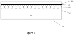
- FIG 1 a schematic cross-section of a front plane laminate (“FPL") 100 is provided.
- the FPL 100 is similar to those described in aforementioned U.S. Patent No. 6,982,178 .
- the FPL 100 may comprise, in order, a light-transmissive electrically-conductive layer; a layer of a solid electro-optic medium in electrical contact with the electrically-conductive layer; an adhesive layer; and a release sheet.
- the light-transmissive electrically-conductive layer 104 is applied to a light-transmissive substrate 102, which is preferably flexible, in the sense that the substrate can be manually wrapped around a drum 10 inches (254 mm) in diameter, for example, without permanent deformation.
- the term "light-transmissive" is used herein throughout the specification and claims to mean that the layer thus designated transmits sufficient light to enable an observer, looking through that layer, to observe the change in display states of the electro-optic medium, which will normally be viewed through the electrically-conductive layer and adjacent substrate (if present); in cases where the electro-optic medium displays a change in reflectivity at non-visible wavelengths, the term “light-transmissive” should of course be interpreted to refer to transmission of the relevant non-visible wavelengths.
- the substrate 102 may be manufactured from glass or a polymeric film, for example, and may have a thickness in the range of about 1 to about 25 mil (25 to 634 ⁇ m), preferably about 2 to about 10 mil (51 to 254 ⁇ m).
- the top conductive layer 104 may comprise a thin metal or metal oxide layer of, for example, ITO, or may be a conductive polymer, such as PEDOT.
- a coating of electro-optic medium 106 is applied over the top conductive layer 104, such that the electro-optic medium 106 is in electrical contact with the top conductive layer 104.
- the electro-optic medium 106 may, preferably, be in the form of an opposite charge dual particle encapsulated electrophoretic medium of the type described in U.S. Patent Application 2002/0185378 .
- the medium may comprise dispersion media encapsulated within a binder.
- the dispersion media may contain a hydrocarbon-based liquid in which are suspended negatively charged white particles and positively charged black particles.
- the white particles may move to the positive electrode and the black particles may move to the negative electrode, for example, so that the electro-optic medium 106 appears, to an observer viewing the display through the substrate 102, white or black depending upon whether the top conductive layer 104 is positive or negative relative to the backplane at any point within the final display.
- the electro-optic medium 106 may alternatively comprise a plurality of colored particles in addition to black and/or white particles, for example, each color having a respective charge polarity and strength.
- a layer of lamination adhesive 108 may be coated over the electro-optic medium layer 106, and a release layer 110 may be applied over the adhesive layer 108.
- the release layer 110 may be a PET film, for example, that is approximately 7 mil in thickness, which may be provided with any appropriate release coating, for example a silicone coating.
- the presence of this lamination adhesive layer affects the electro-optic characteristics of the displays.
- the electrical conductivity of the lamination adhesive layer affects both the low temperature performance and the resolution of the display.
- the low temperature performance of the display may be improved by increasing the conductivity of the lamination adhesive layer, for example by doping the layer with tetrabutylammonium hexafluorophosphate or other materials as described in U.S. Patent Nos.
- the FPL may optionally include a thin second conductive layer, preferably of aluminum, between the release sheet 110 and the laminate adhesive 108 that may be removed with the release sheet 110.
- the second conductive layer may be used for testing of the electro-optic medium.
- the FPL may also be provided in other forms, such as a "double release sheet” as described in U.S. Patent No. 7,561,324 or an "inverted front plane laminate", as described in U. S. Patent No. 7,839,564 .
- the backplane 200 may include a plurality of layers that may be flexible.
- the underlying substrate may be formed from an ablatable polymeric material, such as a polyimide, for example.
- the substrate may also include other optional layers such as a reflective/moisture barrier. Any method known by those of skill in the art may be used to fabricate a backplane for use in the lamination processes and laminated displays of the present invention, such as U.S. Patent 7,223,672 .
- backplanes There are three main categories of backplanes: an active matrix, a passive matrix, and a direct drive backplane. Any type of backplane may be used in the various embodiments of the present invention in order to provide a top plane connection within the perimeter of the laminate.
- an array of thin film transistors are formed on the surface of a substrate and each transistor acts as a switch for a pixel.
- the TFT is addressed by a set of narrow multiplexed electrodes (gate lines and source lines).
- a pixel is addressed by applying voltage to a gate line that switches the TFT on and allows a charge from the source line to flow on to the rear electrode. This sets up a voltage across the pixel and turns it on.
- Passive-matrix backplanes use a simple grid to supply the charge to a particular pixel on the display.
- the grids are formed on top and bottom substrates.
- One substrate forms the “columns” and the other substrate forms the "rows”.
- the wiring of the column or rows is made from a transparent conductive material, usually indium-tin oxide (ITO).
- ITO indium-tin oxide
- the rows or columns are connected to integrated circuits that control when a charge is sent down a particular column or row.
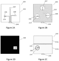
- the bottom substrate 202 may include an electrical connector 204 located on an edge of the substrate 202 from which a plurality of conductors 206, 207, 208 extends. Any method known by those of skill in the art may be used to trace the conductors 206, 207, 208 onto the surface of the substrate 202, such as plating methods.
- the plurality of conductors one of the conductors 206 is used to form the top plane connection with the top conductive layer of the FPL.
- the conductor 206 used to form the top plane connection may include a cut-out 214, which will be described in greater detail below.
- the substrate 202 of the direct drive backplane 200 will then be coated with an insulating layer 210, as illustrated in Figure 2B .
- the insulating layer 210 is preferably made from a dielectric material, such as silicon nitride, an insulating polymer, or cross-linkable monomer or oligomer.
- the insulating layer 210 is applied to cover a majority of the conductive material, while leaving the end portions of the conductors 206, 207, 208 exposed.
- a segmented conductive layer 212a, 212b is then applied over the conductors 207, 208 that will not form part of the top plane connection, as illustrated in Figure 2C .
- the segmented conductive layers 212a, 212b are applied such that each segment is electrically connected to a respective conductor 207, 208, which may be achieved by leaving an area of insulating material 210 between the segments 212a, 212b.
- the conductive layer is also applied in a manner that will avoid an electrical connection with conductor 206, which will form part of the top plane connection.
- the conductive layer 212b may be applied such that a boundary of insulating layer 210 will remain between the conductor 206 and the conductive layer 212b, as illustrated in Figure 2C .
- Assembly of an electro-optic display using FPL 100 may be effected by removing the release sheet 110 and contacting the adhesive layer 108 with the backplane 200 under conditions effective to cause the adhesive layer 108 to adhere to the backplane 200, thereby securing the adhesive layer 108, layer of electro-optic medium 106 and electrically-conductive top layer 104 to the backplane 200, and then cut into pieces of any size needed for use with specific backplanes.
- the backplane 200 and FPL 100 must be laminated, such that the end of the conductor 206 is electrically connected only to a specific area of the top conductive layer 104 that is exposed through the adhesive layer 108, as illustrated in Figure 2D .
- the process according to various embodiments of the present invention overcomes the disadvantages in previous lamination techniques by utilizing a cut-out 214 that is scored within the perimeter of an end portion of a conductor that forms a part of the top plane connection.
- the FPL must first be laminated to a backplane having a cut-out.
- the FPL can be cut larger than the final display size and could even be a continuous sheet as in a roll-to-roll process. This allows for coarse tolerances in alignment of the FPL and backplane, which is especially helpful for large displays.
- the display can be cut to its final size, potentially using alignment marks or pins on the backplane to allow for precisely aligning the cut to the backplane.
- the cut-out 214 in the rear surface of the backplane 200 may form a tab or flap, so that the cut-out 214 may be easily removed post-lamination of the backplane to the FPL.
- the cut-out may be provided in a variety of shapes, such as rectangular, circular, etc., and any method know to those of skill in the art for scoring a backplane material may be used, such as laser-cutting, for example. If the backplane is made of glass, laser-cutting may be used, as well as other methods, such as cutting or drilling with a diamond saw or drill, for example.
- a rectangular-shaped tab may be made from two substantially parallel cuts originating at the edge of the backplane, such as the tab 214 illustrated in Figure 3E .
- the cuts may converge to form a tapered tab, similar to a triangular or trapezoidal shape, for example.
- a hole may be drilled into the backplane and covered with a removable cover, such as a sticker, having an area at least as large as the opening. The removable cover would serve as the removable tab.
- the cut-out 214 may be a segmented circle and a slot 215 may be incorporated about the center of the segmented circle 214.
- the slot 215 may be dimensioned to receive a tool, such as a flat-head screwdriver, for example, and the thin strips of material separating the segments of the circle 214 may be sufficiently thin, such that rotation of the cut-out 214 with a tool will cause the thin strips of material to break and allow removal of the cut-out 214 from the substrate 202.
- the cut-out 214 may be divided into any number of segments, preferably at least two, and the slot 215 may be any shape that is able to mate with a tool.
- the slot 215 may be in the form of a cross to accommodate a Philips screwdriver or a hexagon to accommodate an Allen wrench.
- the lamination of the FPL to the backplane may advantageously be carried out by vacuum lamination.
- Vacuum lamination is effective in expelling air from between the two materials being laminated, thus avoiding unwanted air bubbles in the final display; such air bubbles may introduce undesirable artifacts in the images produced on the display.
- vacuum lamination of the two parts of an electro-optic display in this manner imposes stringent requirements upon the lamination adhesive used, especially in the case of a display using an encapsulated electrophoretic medium.
- the lamination adhesive should have sufficient adhesive strength to bind the electro-optic layer to the backplane, and in the case of an encapsulated electrophoretic medium, the adhesive should also have sufficient adhesive strength to mechanically hold the capsules together.
- the adhesive is preferably chemically compatible with all the other materials in the display. If the electro-optic display is to be of a flexible type, the adhesive should have sufficient flexibility not to introduce defects into the display when the display is flexed.
- the lamination adhesive should have adequate flow properties at the lamination temperature to ensure high quality lamination. Furthermore, the lamination temperature is preferably as low as possible.
- An example of a useful lamination adhesive that may be incorporated in the various embodiments of the present invention an aqueous polyurethane dispersion known as a "TMXDI/PPO" dispersion, as described in U.S. Patent Application Publication No. 2005/0107564 .
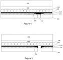
- Figures 4 to 7 are a partial schematic cross-section along axis I-I of Figure 3A . As illustrated in Figure 4 , the cut-out 214 in the substrate 202 of the backplane was incorporated prior to formation of the conductor 206.
- the material of the conductor 206 fills the space between the cut-out 214 and the substrate 202. Therefore, it is preferred to form the cut-out 214 prior to forming the conductors 206, as best shown in Figure 7 , in order to increase the surface contact area of the portion of the conductor that will form the top plane connector. It is also preferred to provide a cut-out 214 in the form of a tab, for example, rather than a through-hole in the substrate 202 to provide a backing for the FPL during the lamination process and reduce the likelihood of forming a divot or deformation in the surface of the FPL over the area of the through-hole.
- the cut-out 214 may be removed, as illustrated in Figure 5 . Because the adhesive layer 108 is laminated to the substrate 202, removal of the cut-out 214 will also result in removal in the section of the adhesive layer 108. Therefore, removal of the cut-out 214 will accomplish a substantial portion of the cleaning required to expose the top conductive layer 104.
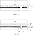
- a solvent may be used in a manual or automated cleaning process to expose a portion of the electro-optic medium 106 within the boundary of the through-hole, as illustrated in Figure 6 .
- the solvent should be selected that will dissolve the electro-optic layer without damaging the top conductive layer.
- the size of the cut-out should be selected, such that sufficient space is provided following its removal to allow for ease and efficiency of cleaning and to maximize the surface area for electrical contact with the overlying conductor.
- a conductive material 216 may be filled in the open space to electrically connect the conductor 206 to the top conductive layer 104, thus forming the top plane connection.
- the conductive material may be any conductive filler known to those of skill in the art, such as a silver or carbon filled epoxy.
- an insulating barrier (not shown) may be applied over any conductive filler by laminating or dispensing a thin layer of insulating material over an area that is at least as large as the area of the conductive filler on the exposed side of the backplane.
- a double-sided backplane may be incorporated into the laminate.
- a double-sided backplane differs from the backplane illustrated in Figures 4 to 7 in that the material used to the form the conductor for the top plane connection may be printed on both sides of the backplane substrate.
- the material used to form the conductor 206 has been printed on both sides of the substrate 202, such that the conductor 206 will cover generally the entirety of the through-hole formed after removal of the cut-out.
- the remaining steps of the top plane connection process will be the same as those described above.
- the surface area of the conductor is larger relative to the embodiment illustrated in Figures 4 to 7 . This allows for more connection surface area between the conductor in the backplane and the conductive fill material which will be dispensed into the plated through-hole via.
- a double sided backplane similar to a single sided backplane, may be produced by known PCB or flex-PCB techniques as well as by screen printing.
- the extra screen printing step where conductor material is applied to the bottom side of the substrate around the cut-out would add extra area for making the top plane connection thereby improving the overall display reliability.
- FIG. 9 Another embodiment comprising a double sided backplane is illustrated in Figure 9 .
- the through-hole created by removing the cut-out to form the top plane connection may not be ideally sized, such that it may simultaneously be used as a conductive via.
- the embodiment illustrated in Figure 9 instead provides two separate pathways through the substrate 202, one conductive via 220 for the conductor 206, which is screen printed on both sides of the substrate 202 and covered with an insulating layer 210, as well as one through-hole filled with conductive material 216 to from the top plane connection between the conductor 206 and the top conductive layer 104.
- the laminate may include a plurality of vias to ensure connectivity between the screen printed conductors on either side of the backplane substrate and the conductive layer on the walls of the through-hole for the top plane connection is not necessary.
- the various embodiments of the present invention simplify the production of custom large area displays where alignment jigs and other equipment are not available for precision aligned lamination. It also makes possible the use of roll-to-roll production of displays using continuous rolls of FPL and backplane.
- the electrical connection between the top conductive layer and the backplane will be robust and reliable due to the relatively large area of exposed top conductive layer.
- small volume orders can be made with high yield, especially in applications in which the TPC cannot be hidden behind a bezel or frame and must be small.
- the small TPC provided using the process according various embodiments of the invention may be highly desirable in such applications.
Landscapes
- Physics & Mathematics (AREA)
- Nonlinear Science (AREA)
- General Physics & Mathematics (AREA)
- Optics & Photonics (AREA)
- Chemical & Material Sciences (AREA)
- Life Sciences & Earth Sciences (AREA)
- Health & Medical Sciences (AREA)
- Chemical Kinetics & Catalysis (AREA)
- Electrochemistry (AREA)
- Molecular Biology (AREA)
- Mathematical Physics (AREA)
- Crystallography & Structural Chemistry (AREA)
- Electrochromic Elements, Electrophoresis, Or Variable Reflection Or Absorption Elements (AREA)
- Devices For Indicating Variable Information By Combining Individual Elements (AREA)
Claims (10)
- Verfahren zur Bildung einer elektrooptischen Anzeige, umfassend:Bilden eines Frontebenenlaminats (100), das in dieser Reihenfolge ein erstes Substrat (102), eine erste leitfähige Schicht (104), eine Schicht aus elektrooptischem Medium (106) und einen Klebstoff (108) umfasst, wobei das erste Substrat (102) und die erste leitfähige Schicht (104) transparent sind; undBeschichten eines zweiten Substrats (202), das eine Vielzahl von Leitern (204, 206, 207, 208) umfasst, mit einer Isolierschicht (210) und einer zweiten leitfähigen Schicht (212b), um eine Rückwand (Backplane) (200) bereitzustellen;wobei das Verfahren gekennzeichnet ist durch:Ritzen des zweiten Substrats (202), um einen entfernbaren Anteil (214) zu bilden;Laminieren des Frontebenenlaminats (100) auf die Backplane (200);Entfernen des entfernbaren Anteils (214) von dem zweiten Substrat (202), um eine Öffnung in der Backplane (200) bereitzustellen; undFüllen der Öffnung mit einem leitfähigen Material (216), um eine elektrische Verbindung zwischen der ersten leitfähigen Schicht (104) und einem (206) von der Vielzahl der Leiter (204, 206, 207, 208) bereitzustellen.
- Verfahren nach Anspruch 1, wobei der entfernbare Anteil (214) in dem zweiten Substrat (202) in der Nähe des einen Leiters (206) geritzt wird.
- Verfahren nach Anspruch 1, wobei der Ritzschritt vor dem Beschichten des zweiten Substrats (202) mit der Isolierschicht (210) und der zweiten leitfähigen Schicht (212b) stattfindet.
- Verfahren nach Anspruch 1, wobei der Entfernungsschritt mindestens eines von dem elektrooptischen Medium (106) und dem Klebstoff (108) innerhalb der Öffnung exponiert.
- Verfahren nach Anspruch 4, des Weiteren umfassend Entfernen von mindestens einem Teil des elektrooptischen Mediums (106) und des Klebstoffs (108) innerhalb der Öffnung nach dem Laminierungsschritt, um die erste leitfähige Schicht (104) zu exponieren.
- Verfahren nach Anspruch 1, wobei der entfernbare Anteil (214) des zweiten Substrats (202) in Form einer Lasche vorliegt.
- Verfahren nach Anspruch 1, wobei die zweite leitfähige Schicht (212b) auf zwei gegenüber liegende Oberflächen des zweiten Substrats (202) appliziert wird.
- Verfahren nach Anspruch 1, wobei der entfernbare Anteil (214) vor dem Laminierungsschritt entfernt wird.
- Verfahren nach Anspruch 8, wobei der eine Leiter (206) auf die Oberfläche der Öffnung plattiert wird, bevor das zweite Substrat (202) mit der Isolierschicht (210) und der zweiten leitfähigen Schicht (212b) beschichtet wird.
- Elektrooptische Anzeige, die gemäß dem Verfahren nach Anspruch 1 gefertigt ist.
Priority Applications (2)
| Application Number | Priority Date | Filing Date | Title |
|---|---|---|---|
| EP25156913.3A EP4550042B1 (de) | 2016-11-30 | 2017-11-15 | Laminierte elektrooptische anzeigen und verfahren zu ihrer herstellung |
| EP21206101.4A EP3992706B1 (de) | 2016-11-30 | 2017-11-15 | Laminierte elektrooptische anzeigen und verfahren zur herstellung davon |
Applications Claiming Priority (2)
| Application Number | Priority Date | Filing Date | Title |
|---|---|---|---|
| US201662427970P | 2016-11-30 | 2016-11-30 | |
| PCT/US2017/061710 WO2018102126A1 (en) | 2016-11-30 | 2017-11-15 | Laminated electro-optic displays and methods of making the same |
Related Child Applications (3)
| Application Number | Title | Priority Date | Filing Date |
|---|---|---|---|
| EP21206101.4A Division EP3992706B1 (de) | 2016-11-30 | 2017-11-15 | Laminierte elektrooptische anzeigen und verfahren zur herstellung davon |
| EP21206101.4A Division-Into EP3992706B1 (de) | 2016-11-30 | 2017-11-15 | Laminierte elektrooptische anzeigen und verfahren zur herstellung davon |
| EP25156913.3A Division EP4550042B1 (de) | 2016-11-30 | 2017-11-15 | Laminierte elektrooptische anzeigen und verfahren zu ihrer herstellung |
Publications (3)
| Publication Number | Publication Date |
|---|---|
| EP3548966A4 EP3548966A4 (de) | 2019-10-09 |
| EP3548966A1 EP3548966A1 (de) | 2019-10-09 |
| EP3548966B1 true EP3548966B1 (de) | 2022-01-19 |
Family
ID=62190132
Family Applications (3)
| Application Number | Title | Priority Date | Filing Date |
|---|---|---|---|
| EP17875756.3A Active EP3548966B1 (de) | 2016-11-30 | 2017-11-15 | Laminierte elektrooptische anzeigen und verfahren zur herstellung davon |
| EP25156913.3A Active EP4550042B1 (de) | 2016-11-30 | 2017-11-15 | Laminierte elektrooptische anzeigen und verfahren zu ihrer herstellung |
| EP21206101.4A Active EP3992706B1 (de) | 2016-11-30 | 2017-11-15 | Laminierte elektrooptische anzeigen und verfahren zur herstellung davon |
Family Applications After (2)
| Application Number | Title | Priority Date | Filing Date |
|---|---|---|---|
| EP25156913.3A Active EP4550042B1 (de) | 2016-11-30 | 2017-11-15 | Laminierte elektrooptische anzeigen und verfahren zu ihrer herstellung |
| EP21206101.4A Active EP3992706B1 (de) | 2016-11-30 | 2017-11-15 | Laminierte elektrooptische anzeigen und verfahren zur herstellung davon |
Country Status (9)
| Country | Link |
|---|---|
| US (3) | US10503041B2 (de) |
| EP (3) | EP3548966B1 (de) |
| JP (2) | JP6764038B2 (de) |
| KR (1) | KR102308588B1 (de) |
| CN (2) | CN109983399B (de) |
| ES (1) | ES3020088T3 (de) |
| PL (1) | PL3992706T3 (de) |
| TW (2) | TWI754917B (de) |
| WO (1) | WO2018102126A1 (de) |
Families Citing this family (24)
| Publication number | Priority date | Publication date | Assignee | Title |
|---|---|---|---|---|
| CN107315283B (zh) * | 2017-08-17 | 2021-03-05 | 京东方科技集团股份有限公司 | 背光模组、显示装置和调节背光模组出光亮度的方法 |
| CN109870837B (zh) * | 2017-12-05 | 2021-10-15 | 华为终端有限公司 | 显示组件、显示器、终端及显示器拆卸方法 |
| KR102599722B1 (ko) * | 2018-12-28 | 2023-11-09 | 삼성디스플레이 주식회사 | 표시 패널 및 이를 포함하는 타일드 표시 장치 |
| CA3126042C (en) * | 2019-01-21 | 2023-09-12 | Kyushu Nanotec Optics Co., Ltd. | Method for attaching electrode to liquid crystal element |
| KR102925199B1 (ko) * | 2020-06-30 | 2026-02-10 | 엘지이노텍 주식회사 | 광 경로 제어 부재 및 이를 포함하는 디스플레이 장치 |
| KR102818504B1 (ko) * | 2020-06-30 | 2025-06-10 | 엘지이노텍 주식회사 | 광 경로 제어 부재 및 이를 포함하는 디스플레이 장치 |
| CN116324609A (zh) * | 2020-07-22 | 2023-06-23 | 伊英克公司 | 包含集成的导电边缘密封件的电光装置和用于生产电光装置的方法 |
| KR20220021966A (ko) * | 2020-08-13 | 2022-02-23 | 삼성디스플레이 주식회사 | 표시 패널, 이의 제조 방법 및 표시 패널을 포함하는 표시 장치 |
| WO2022072500A1 (en) * | 2020-10-02 | 2022-04-07 | E Ink Corporation | Front plane laminates with outer surface electrical connections |
| JP7688154B2 (ja) | 2021-04-16 | 2025-06-03 | イー インク コーポレイション | 薄型縁シールを伴う電気泳動ディスプレイ |
| EP4381346A4 (de) * | 2021-08-04 | 2025-07-02 | E Ink Corp | Elektrophoretische anzeige mit dielektrischer beschichtung auf der elektrode |
| CN118696269A (zh) * | 2022-02-25 | 2024-09-24 | 伊英克公司 | 具有边缘密封部件的电光显示器及其制造方法 |
| WO2023211699A1 (en) * | 2022-04-27 | 2023-11-02 | E Ink Corporation | Electro-optic display stacks with segmented electrodes and methods of making the same |
| CN218497311U (zh) * | 2022-10-09 | 2023-02-17 | 汉朔科技股份有限公司 | 显示区域具有凹槽的电子纸屏幕 |
| TWI870787B (zh) * | 2023-02-24 | 2025-01-21 | 元太科技工業股份有限公司 | 顯示裝置 |
| WO2024224322A1 (en) * | 2023-04-28 | 2024-10-31 | Gentex Corporation | Double-sided conducting films |
| US20250053058A1 (en) | 2023-08-08 | 2025-02-13 | E Ink Corporation | Backplanes for segmented electro-optic displays and methods of manufacturing same |
| WO2025147504A1 (en) | 2024-01-05 | 2025-07-10 | E Ink Corporation | An electrophoretic medium comprising particles having a pigment core and a polymeric shell |
| US20250224646A1 (en) | 2024-01-08 | 2025-07-10 | E Ink Corporation | Adhesive Layer Comprising Conductive Filler Particles and a Polymeric Dispersant |
| US20250237922A1 (en) | 2024-01-19 | 2025-07-24 | E Ink Corporation | Flexible segmented electro-optic displays and methods of manufacture |
| WO2025230802A1 (en) | 2024-04-30 | 2025-11-06 | E Ink Corporation | A variable light transmission device comprising microcells |
| US20250370306A1 (en) | 2024-05-30 | 2025-12-04 | E Ink Corporation | Chemically-Resistant Multi-Layered Electro-Optic Device and a Method of Making the Same |
| WO2026006119A1 (en) | 2024-06-26 | 2026-01-02 | E Ink Corporation | A variable light transmission device comprising microcells |
| WO2026006234A1 (en) | 2024-06-26 | 2026-01-02 | E Ink Corporation | A variable light transmission device comprising microcells |
Citations (1)
| Publication number | Priority date | Publication date | Assignee | Title |
|---|---|---|---|---|
| EP2877895B1 (de) * | 2012-07-27 | 2017-09-06 | E Ink Corporation | Verfahren zur herstellung von elektrooptischen anzeigen |
Family Cites Families (66)
| Publication number | Priority date | Publication date | Assignee | Title |
|---|---|---|---|---|
| US55091A (en) | 1866-05-29 | Improvement in portable field-fence | ||
| US6137467A (en) | 1995-01-03 | 2000-10-24 | Xerox Corporation | Optically sensitive electric paper |
| US7411719B2 (en) | 1995-07-20 | 2008-08-12 | E Ink Corporation | Electrophoretic medium and process for the production thereof |
| US6866760B2 (en) | 1998-08-27 | 2005-03-15 | E Ink Corporation | Electrophoretic medium and process for the production thereof |
| US5760761A (en) | 1995-12-15 | 1998-06-02 | Xerox Corporation | Highlight color twisting ball display |
| US5808783A (en) | 1996-06-27 | 1998-09-15 | Xerox Corporation | High reflectance gyricon display |
| US6055091A (en) | 1996-06-27 | 2000-04-25 | Xerox Corporation | Twisting-cylinder display |
| US5777782A (en) | 1996-12-24 | 1998-07-07 | Xerox Corporation | Auxiliary optics for a twisting ball display |
| US6301038B1 (en) | 1997-02-06 | 2001-10-09 | University College Dublin | Electrochromic system |
| US7002728B2 (en) | 1997-08-28 | 2006-02-21 | E Ink Corporation | Electrophoretic particles, and processes for the production thereof |
| US6054071A (en) | 1998-01-28 | 2000-04-25 | Xerox Corporation | Poled electrets for gyricon-based electric-paper displays |
| US7075502B1 (en) | 1998-04-10 | 2006-07-11 | E Ink Corporation | Full color reflective display with multichromatic sub-pixels |
| US6241921B1 (en) | 1998-05-15 | 2001-06-05 | Massachusetts Institute Of Technology | Heterogeneous display elements and methods for their fabrication |
| US6128124A (en) | 1998-10-16 | 2000-10-03 | Xerox Corporation | Additive color electric paper without registration or alignment of individual elements |
| US6147791A (en) | 1998-11-25 | 2000-11-14 | Xerox Corporation | Gyricon displays utilizing rotating elements and magnetic latching |
| US6097531A (en) | 1998-11-25 | 2000-08-01 | Xerox Corporation | Method of making uniformly magnetized elements for a gyricon display |
| US6312304B1 (en) * | 1998-12-15 | 2001-11-06 | E Ink Corporation | Assembly of microencapsulated electronic displays |
| US7012600B2 (en) | 1999-04-30 | 2006-03-14 | E Ink Corporation | Methods for driving bistable electro-optic displays, and apparatus for use therein |
| US8009348B2 (en) | 1999-05-03 | 2011-08-30 | E Ink Corporation | Machine-readable displays |
| EP1500969A1 (de) | 1999-10-11 | 2005-01-26 | University College Dublin | Verbindung und ihrer Verwendung in elektrochromen Vorrichtungen |
| US7715088B2 (en) | 2000-03-03 | 2010-05-11 | Sipix Imaging, Inc. | Electrophoretic display |
| AU2001259451A1 (en) * | 2000-05-04 | 2001-11-12 | Schott Donnelly Llc | Chromogenic glazing |
| US7030854B2 (en) | 2001-03-13 | 2006-04-18 | E Ink Corporation | Apparatus for displaying drawings |
| US7679814B2 (en) | 2001-04-02 | 2010-03-16 | E Ink Corporation | Materials for use in electrophoretic displays |
| JP4188091B2 (ja) | 2001-05-15 | 2008-11-26 | イー インク コーポレイション | 電気泳動粒子 |
| US20020188053A1 (en) | 2001-06-04 | 2002-12-12 | Sipix Imaging, Inc. | Composition and process for the sealing of microcups in roll-to-roll display manufacturing |
| US7535624B2 (en) | 2001-07-09 | 2009-05-19 | E Ink Corporation | Electro-optic display and materials for use therein |
| US6982178B2 (en) * | 2002-06-10 | 2006-01-03 | E Ink Corporation | Components and methods for use in electro-optic displays |
| US6950220B2 (en) | 2002-03-18 | 2005-09-27 | E Ink Corporation | Electro-optic displays, and methods for driving same |
| US7223672B2 (en) | 2002-04-24 | 2007-05-29 | E Ink Corporation | Processes for forming backplanes for electro-optic displays |
| WO2003092077A2 (en) | 2002-04-24 | 2003-11-06 | E Ink Corporation | Electronic displays |
| CN101109885B (zh) | 2002-09-03 | 2012-06-13 | 伊英克公司 | 电光显示器 |
| US7839564B2 (en) | 2002-09-03 | 2010-11-23 | E Ink Corporation | Components and methods for use in electro-optic displays |
| TWI229230B (en) | 2002-10-31 | 2005-03-11 | Sipix Imaging Inc | An improved electrophoretic display and novel process for its manufacture |
| US6922276B2 (en) | 2002-12-23 | 2005-07-26 | E Ink Corporation | Flexible electro-optic displays |
| US7339715B2 (en) | 2003-03-25 | 2008-03-04 | E Ink Corporation | Processes for the production of electrophoretic displays |
| US7012735B2 (en) | 2003-03-27 | 2006-03-14 | E Ink Corporaiton | Electro-optic assemblies, and materials for use therein |
| CN101930118B (zh) | 2003-10-08 | 2013-05-29 | 伊英克公司 | 电润湿显示器 |
| CN101382719B (zh) * | 2003-10-24 | 2012-04-04 | 伊英克公司 | 电光显示器 |
| EP1680774B9 (de) | 2003-11-05 | 2018-05-16 | E Ink Corporation | Elektrophoretisches medium für elektro-optische bildschirme |
| US7342068B2 (en) | 2003-11-18 | 2008-03-11 | Air Products And Chemicals, Inc. | Aqueous polyurethane dispersion and method for making and using same |
| US7453445B2 (en) | 2004-08-13 | 2008-11-18 | E Ink Corproation | Methods for driving electro-optic displays |
| US8576162B2 (en) | 2005-03-14 | 2013-11-05 | Sipix Imaging, Inc. | Manufacturing processes of backplane for segment displays |
| CN101371180A (zh) * | 2005-10-18 | 2009-02-18 | 伊英克公司 | 用于电光显示器的部件 |
| US8173519B2 (en) * | 2006-03-03 | 2012-05-08 | Semiconductor Energy Laboratory Co., Ltd. | Method for manufacturing semiconductor device |
| US7733554B2 (en) | 2006-03-08 | 2010-06-08 | E Ink Corporation | Electro-optic displays, and materials and methods for production thereof |
| US7843624B2 (en) | 2006-03-08 | 2010-11-30 | E Ink Corporation | Electro-optic displays, and materials and methods for production thereof |
| JP4211808B2 (ja) * | 2006-06-23 | 2009-01-21 | セイコーエプソン株式会社 | 電気光学装置及び電子機器 |
| US20150005720A1 (en) | 2006-07-18 | 2015-01-01 | E Ink California, Llc | Electrophoretic display |
| TWI361331B (en) | 2007-06-01 | 2012-04-01 | Pervasive Display Co Ltd | E-paper apparatus |
| JP5521309B2 (ja) | 2008-10-29 | 2014-06-11 | セイコーエプソン株式会社 | 電気泳動表示素子の製造方法 |
| JP2012014206A (ja) | 2008-10-31 | 2012-01-19 | Nissha Printing Co Ltd | タッチ入力機能付き保護パネルのfpc接続方法 |
| JP2010181768A (ja) * | 2009-02-09 | 2010-08-19 | Citizen Holdings Co Ltd | 電気泳動型表示装置 |
| JP2011099948A (ja) * | 2009-11-05 | 2011-05-19 | Panasonic Corp | 電子ペーパ及び電子ペーパ書き込み装置 |
| KR101203388B1 (ko) | 2010-04-28 | 2012-11-21 | 주식회사 이미지앤머터리얼스 | 전기 광학 디스플레이 장치용 입자, 그 제조 방법 및 전기 영동 디스플레이 장치 |
| JP2012003988A (ja) * | 2010-06-17 | 2012-01-05 | Hitachi Displays Ltd | 有機エレクトロルミネッセンスパネルの製造方法 |
| JP2012119532A (ja) * | 2010-12-01 | 2012-06-21 | Seiko Epson Corp | 薄膜トランジスタ形成用基板、半導体装置、電気装置 |
| JP2012181445A (ja) * | 2011-03-02 | 2012-09-20 | Seiko Epson Corp | 電気装置 |
| WO2012128105A1 (ja) * | 2011-03-19 | 2012-09-27 | シャープ株式会社 | 表示素子、表示装置、および表示方法 |
| JP4882031B1 (ja) | 2011-04-26 | 2012-02-22 | 株式会社サクラクレパス | 電気泳動表示装置 |
| US10042189B2 (en) | 2011-12-01 | 2018-08-07 | Avery Dennison Retail Information Services, Llc | Backplane for electrophoretic display |
| GB201208680D0 (en) * | 2012-05-17 | 2012-06-27 | Origold As | Method of manufacturing an electronic card |
| US9279906B2 (en) | 2012-08-31 | 2016-03-08 | E Ink California, Llc | Microstructure film |
| ES2661512T3 (es) * | 2013-09-17 | 2018-04-02 | Essilor International | Composición electrocrómica |
| WO2015148398A1 (en) | 2014-03-25 | 2015-10-01 | E Ink California, Llc | Magnetophoretic display assembly and driving scheme |
| US20160012710A1 (en) | 2014-07-10 | 2016-01-14 | Sipix Technology Inc. | Smart medication device |
-
2017
- 2017-11-03 US US15/802,571 patent/US10503041B2/en active Active
- 2017-11-15 PL PL21206101.4T patent/PL3992706T3/pl unknown
- 2017-11-15 ES ES21206101T patent/ES3020088T3/es active Active
- 2017-11-15 EP EP17875756.3A patent/EP3548966B1/de active Active
- 2017-11-15 CN CN201780071231.3A patent/CN109983399B/zh active Active
- 2017-11-15 EP EP25156913.3A patent/EP4550042B1/de active Active
- 2017-11-15 KR KR1020197015079A patent/KR102308588B1/ko active Active
- 2017-11-15 JP JP2019547577A patent/JP6764038B2/ja active Active
- 2017-11-15 EP EP21206101.4A patent/EP3992706B1/de active Active
- 2017-11-15 WO PCT/US2017/061710 patent/WO2018102126A1/en not_active Ceased
- 2017-11-15 CN CN202210696255.0A patent/CN114995006B/zh active Active
- 2017-11-20 TW TW109112615A patent/TWI754917B/zh active
- 2017-11-20 TW TW106140140A patent/TWI691773B/zh active
-
2019
- 2019-11-06 US US16/675,620 patent/US11397362B2/en active Active
-
2020
- 2020-09-10 JP JP2020151834A patent/JP2021009394A/ja active Pending
-
2022
- 2022-02-28 US US17/682,627 patent/US11829047B2/en active Active
Patent Citations (1)
| Publication number | Priority date | Publication date | Assignee | Title |
|---|---|---|---|---|
| EP2877895B1 (de) * | 2012-07-27 | 2017-09-06 | E Ink Corporation | Verfahren zur herstellung von elektrooptischen anzeigen |
Also Published As
| Publication number | Publication date |
|---|---|
| EP3992706B1 (de) | 2025-03-19 |
| TW202028836A (zh) | 2020-08-01 |
| CN109983399B (zh) | 2022-07-12 |
| EP3548966A4 (de) | 2019-10-09 |
| CN109983399A (zh) | 2019-07-05 |
| KR20190060889A (ko) | 2019-06-03 |
| TWI754917B (zh) | 2022-02-11 |
| KR102308588B1 (ko) | 2021-10-01 |
| US20180149942A1 (en) | 2018-05-31 |
| US20220179276A1 (en) | 2022-06-09 |
| JP6764038B2 (ja) | 2020-09-30 |
| JP2019536116A (ja) | 2019-12-12 |
| JP2021009394A (ja) | 2021-01-28 |
| EP4550042A3 (de) | 2025-07-30 |
| US10503041B2 (en) | 2019-12-10 |
| EP4550042A2 (de) | 2025-05-07 |
| US20200073194A1 (en) | 2020-03-05 |
| EP3992706A1 (de) | 2022-05-04 |
| EP4550042B1 (de) | 2026-01-14 |
| TWI691773B (zh) | 2020-04-21 |
| EP3548966A1 (de) | 2019-10-09 |
| WO2018102126A1 (en) | 2018-06-07 |
| TW201825995A (zh) | 2018-07-16 |
| EP4550042C0 (de) | 2026-01-14 |
| CN114995006A (zh) | 2022-09-02 |
| ES3020088T3 (en) | 2025-05-21 |
| CN114995006B (zh) | 2025-11-07 |
| US11829047B2 (en) | 2023-11-28 |
| EP3992706C0 (de) | 2025-03-19 |
| PL3992706T3 (pl) | 2025-07-21 |
| US11397362B2 (en) | 2022-07-26 |
Similar Documents
| Publication | Publication Date | Title |
|---|---|---|
| US11829047B2 (en) | Top plane connections for electro-optic devices including a through-hole in rear substrate | |
| US12038666B2 (en) | Method of forming a top plane connection in an electro-optic device | |
| US9671635B2 (en) | Electro-optic display backplane structures with drive components and pixel electrodes on opposed surfaces | |
| KR102110013B1 (ko) | 백플레인 어셈블리들을 위한 멀티-레이어 확장 전극 구조들 | |
| US10317767B2 (en) | Electro-optic display backplane structure with drive components and pixel electrodes on opposed surfaces | |
| HK40072011A (zh) | 层压电光显示器及其制造方法 | |
| HK40003820B (en) | Laminated electro-optic displays and methods of making the same | |
| HK40003820A (en) | Laminated electro-optic displays and methods of making the same | |
| US20250053058A1 (en) | Backplanes for segmented electro-optic displays and methods of manufacturing same | |
| WO2018187077A1 (en) | Electro-optic display backplane structures with drive components and pixel electrodes on opposed surfaces |
Legal Events
| Date | Code | Title | Description |
|---|---|---|---|
| STAA | Information on the status of an ep patent application or granted ep patent |
Free format text: STATUS: THE INTERNATIONAL PUBLICATION HAS BEEN MADE |
|
| PUAI | Public reference made under article 153(3) epc to a published international application that has entered the european phase |
Free format text: ORIGINAL CODE: 0009012 |
|
| STAA | Information on the status of an ep patent application or granted ep patent |
Free format text: STATUS: REQUEST FOR EXAMINATION WAS MADE |
|
| 17P | Request for examination filed |
Effective date: 20190701 |
|
| A4 | Supplementary search report drawn up and despatched |
Effective date: 20190909 |
|
| AK | Designated contracting states |
Kind code of ref document: A1 Designated state(s): AL AT BE BG CH CY CZ DE DK EE ES FI FR GB GR HR HU IE IS IT LI LT LU LV MC MK MT NL NO PL PT RO RS SE SI SK SM TR |
|
| AX | Request for extension of the european patent |
Extension state: BA ME |
|
| DAV | Request for validation of the european patent (deleted) | ||
| DAX | Request for extension of the european patent (deleted) | ||
| GRAP | Despatch of communication of intention to grant a patent |
Free format text: ORIGINAL CODE: EPIDOSNIGR1 |
|
| STAA | Information on the status of an ep patent application or granted ep patent |
Free format text: STATUS: GRANT OF PATENT IS INTENDED |
|
| INTG | Intention to grant announced |
Effective date: 20210928 |
|
| GRAS | Grant fee paid |
Free format text: ORIGINAL CODE: EPIDOSNIGR3 |
|
| GRAA | (expected) grant |
Free format text: ORIGINAL CODE: 0009210 |
|
| STAA | Information on the status of an ep patent application or granted ep patent |
Free format text: STATUS: THE PATENT HAS BEEN GRANTED |
|
| AK | Designated contracting states |
Kind code of ref document: B1 Designated state(s): AL AT BE BG CH CY CZ DE DK EE ES FI FR GB GR HR HU IE IS IT LI LT LU LV MC MK MT NL NO PL PT RO RS SE SI SK SM TR |
|
| REG | Reference to a national code |
Ref country code: GB Ref legal event code: FG4D |
|
| REG | Reference to a national code |
Ref country code: CH Ref legal event code: EP |
|
| REG | Reference to a national code |
Ref country code: AT Ref legal event code: REF Ref document number: 1464138 Country of ref document: AT Kind code of ref document: T Effective date: 20220215 |
|
| REG | Reference to a national code |
Ref country code: IE Ref legal event code: FG4D |
|
| REG | Reference to a national code |
Ref country code: DE Ref legal event code: R096 Ref document number: 602017052608 Country of ref document: DE |
|
| REG | Reference to a national code |
Ref country code: LT Ref legal event code: MG9D |
|
| REG | Reference to a national code |
Ref country code: NL Ref legal event code: MP Effective date: 20220119 |
|
| REG | Reference to a national code |
Ref country code: AT Ref legal event code: MK05 Ref document number: 1464138 Country of ref document: AT Kind code of ref document: T Effective date: 20220119 |
|
| PG25 | Lapsed in a contracting state [announced via postgrant information from national office to epo] |
Ref country code: NL Free format text: LAPSE BECAUSE OF FAILURE TO SUBMIT A TRANSLATION OF THE DESCRIPTION OR TO PAY THE FEE WITHIN THE PRESCRIBED TIME-LIMIT Effective date: 20220119 |
|
| PG25 | Lapsed in a contracting state [announced via postgrant information from national office to epo] |
Ref country code: SE Free format text: LAPSE BECAUSE OF FAILURE TO SUBMIT A TRANSLATION OF THE DESCRIPTION OR TO PAY THE FEE WITHIN THE PRESCRIBED TIME-LIMIT Effective date: 20220119 Ref country code: RS Free format text: LAPSE BECAUSE OF FAILURE TO SUBMIT A TRANSLATION OF THE DESCRIPTION OR TO PAY THE FEE WITHIN THE PRESCRIBED TIME-LIMIT Effective date: 20220119 Ref country code: PT Free format text: LAPSE BECAUSE OF FAILURE TO SUBMIT A TRANSLATION OF THE DESCRIPTION OR TO PAY THE FEE WITHIN THE PRESCRIBED TIME-LIMIT Effective date: 20220519 Ref country code: NO Free format text: LAPSE BECAUSE OF FAILURE TO SUBMIT A TRANSLATION OF THE DESCRIPTION OR TO PAY THE FEE WITHIN THE PRESCRIBED TIME-LIMIT Effective date: 20220419 Ref country code: LT Free format text: LAPSE BECAUSE OF FAILURE TO SUBMIT A TRANSLATION OF THE DESCRIPTION OR TO PAY THE FEE WITHIN THE PRESCRIBED TIME-LIMIT Effective date: 20220119 Ref country code: HR Free format text: LAPSE BECAUSE OF FAILURE TO SUBMIT A TRANSLATION OF THE DESCRIPTION OR TO PAY THE FEE WITHIN THE PRESCRIBED TIME-LIMIT Effective date: 20220119 Ref country code: ES Free format text: LAPSE BECAUSE OF FAILURE TO SUBMIT A TRANSLATION OF THE DESCRIPTION OR TO PAY THE FEE WITHIN THE PRESCRIBED TIME-LIMIT Effective date: 20220119 Ref country code: BG Free format text: LAPSE BECAUSE OF FAILURE TO SUBMIT A TRANSLATION OF THE DESCRIPTION OR TO PAY THE FEE WITHIN THE PRESCRIBED TIME-LIMIT Effective date: 20220419 |
|
| PG25 | Lapsed in a contracting state [announced via postgrant information from national office to epo] |
Ref country code: PL Free format text: LAPSE BECAUSE OF FAILURE TO SUBMIT A TRANSLATION OF THE DESCRIPTION OR TO PAY THE FEE WITHIN THE PRESCRIBED TIME-LIMIT Effective date: 20220119 Ref country code: LV Free format text: LAPSE BECAUSE OF FAILURE TO SUBMIT A TRANSLATION OF THE DESCRIPTION OR TO PAY THE FEE WITHIN THE PRESCRIBED TIME-LIMIT Effective date: 20220119 Ref country code: GR Free format text: LAPSE BECAUSE OF FAILURE TO SUBMIT A TRANSLATION OF THE DESCRIPTION OR TO PAY THE FEE WITHIN THE PRESCRIBED TIME-LIMIT Effective date: 20220420 Ref country code: FI Free format text: LAPSE BECAUSE OF FAILURE TO SUBMIT A TRANSLATION OF THE DESCRIPTION OR TO PAY THE FEE WITHIN THE PRESCRIBED TIME-LIMIT Effective date: 20220119 Ref country code: AT Free format text: LAPSE BECAUSE OF FAILURE TO SUBMIT A TRANSLATION OF THE DESCRIPTION OR TO PAY THE FEE WITHIN THE PRESCRIBED TIME-LIMIT Effective date: 20220119 |
|
| PG25 | Lapsed in a contracting state [announced via postgrant information from national office to epo] |
Ref country code: IS Free format text: LAPSE BECAUSE OF FAILURE TO SUBMIT A TRANSLATION OF THE DESCRIPTION OR TO PAY THE FEE WITHIN THE PRESCRIBED TIME-LIMIT Effective date: 20220519 |
|
| REG | Reference to a national code |
Ref country code: DE Ref legal event code: R097 Ref document number: 602017052608 Country of ref document: DE |
|
| PG25 | Lapsed in a contracting state [announced via postgrant information from national office to epo] |
Ref country code: SM Free format text: LAPSE BECAUSE OF FAILURE TO SUBMIT A TRANSLATION OF THE DESCRIPTION OR TO PAY THE FEE WITHIN THE PRESCRIBED TIME-LIMIT Effective date: 20220119 Ref country code: SK Free format text: LAPSE BECAUSE OF FAILURE TO SUBMIT A TRANSLATION OF THE DESCRIPTION OR TO PAY THE FEE WITHIN THE PRESCRIBED TIME-LIMIT Effective date: 20220119 Ref country code: RO Free format text: LAPSE BECAUSE OF FAILURE TO SUBMIT A TRANSLATION OF THE DESCRIPTION OR TO PAY THE FEE WITHIN THE PRESCRIBED TIME-LIMIT Effective date: 20220119 Ref country code: EE Free format text: LAPSE BECAUSE OF FAILURE TO SUBMIT A TRANSLATION OF THE DESCRIPTION OR TO PAY THE FEE WITHIN THE PRESCRIBED TIME-LIMIT Effective date: 20220119 Ref country code: DK Free format text: LAPSE BECAUSE OF FAILURE TO SUBMIT A TRANSLATION OF THE DESCRIPTION OR TO PAY THE FEE WITHIN THE PRESCRIBED TIME-LIMIT Effective date: 20220119 Ref country code: CZ Free format text: LAPSE BECAUSE OF FAILURE TO SUBMIT A TRANSLATION OF THE DESCRIPTION OR TO PAY THE FEE WITHIN THE PRESCRIBED TIME-LIMIT Effective date: 20220119 |
|
| PLBE | No opposition filed within time limit |
Free format text: ORIGINAL CODE: 0009261 |
|
| STAA | Information on the status of an ep patent application or granted ep patent |
Free format text: STATUS: NO OPPOSITION FILED WITHIN TIME LIMIT |
|
| PG25 | Lapsed in a contracting state [announced via postgrant information from national office to epo] |
Ref country code: AL Free format text: LAPSE BECAUSE OF FAILURE TO SUBMIT A TRANSLATION OF THE DESCRIPTION OR TO PAY THE FEE WITHIN THE PRESCRIBED TIME-LIMIT Effective date: 20220119 |
|
| 26N | No opposition filed |
Effective date: 20221020 |
|
| PG25 | Lapsed in a contracting state [announced via postgrant information from national office to epo] |
Ref country code: SI Free format text: LAPSE BECAUSE OF FAILURE TO SUBMIT A TRANSLATION OF THE DESCRIPTION OR TO PAY THE FEE WITHIN THE PRESCRIBED TIME-LIMIT Effective date: 20220119 |
|
| PG25 | Lapsed in a contracting state [announced via postgrant information from national office to epo] |
Ref country code: MC Free format text: LAPSE BECAUSE OF FAILURE TO SUBMIT A TRANSLATION OF THE DESCRIPTION OR TO PAY THE FEE WITHIN THE PRESCRIBED TIME-LIMIT Effective date: 20220119 |
|
| REG | Reference to a national code |
Ref country code: CH Ref legal event code: PL |
|
| REG | Reference to a national code |
Ref country code: BE Ref legal event code: MM Effective date: 20221130 |
|
| PG25 | Lapsed in a contracting state [announced via postgrant information from national office to epo] |
Ref country code: LI Free format text: LAPSE BECAUSE OF NON-PAYMENT OF DUE FEES Effective date: 20221130 Ref country code: IT Free format text: LAPSE BECAUSE OF FAILURE TO SUBMIT A TRANSLATION OF THE DESCRIPTION OR TO PAY THE FEE WITHIN THE PRESCRIBED TIME-LIMIT Effective date: 20220119 Ref country code: CH Free format text: LAPSE BECAUSE OF NON-PAYMENT OF DUE FEES Effective date: 20221130 |
|
| PG25 | Lapsed in a contracting state [announced via postgrant information from national office to epo] |
Ref country code: LU Free format text: LAPSE BECAUSE OF NON-PAYMENT OF DUE FEES Effective date: 20221115 |
|
| PG25 | Lapsed in a contracting state [announced via postgrant information from national office to epo] |
Ref country code: IE Free format text: LAPSE BECAUSE OF NON-PAYMENT OF DUE FEES Effective date: 20221115 |
|
| PG25 | Lapsed in a contracting state [announced via postgrant information from national office to epo] |
Ref country code: BE Free format text: LAPSE BECAUSE OF NON-PAYMENT OF DUE FEES Effective date: 20221130 |
|
| PG25 | Lapsed in a contracting state [announced via postgrant information from national office to epo] |
Ref country code: HU Free format text: LAPSE BECAUSE OF FAILURE TO SUBMIT A TRANSLATION OF THE DESCRIPTION OR TO PAY THE FEE WITHIN THE PRESCRIBED TIME-LIMIT; INVALID AB INITIO Effective date: 20171115 |
|
| PG25 | Lapsed in a contracting state [announced via postgrant information from national office to epo] |
Ref country code: CY Free format text: LAPSE BECAUSE OF FAILURE TO SUBMIT A TRANSLATION OF THE DESCRIPTION OR TO PAY THE FEE WITHIN THE PRESCRIBED TIME-LIMIT Effective date: 20220119 |
|
| PG25 | Lapsed in a contracting state [announced via postgrant information from national office to epo] |
Ref country code: MK Free format text: LAPSE BECAUSE OF FAILURE TO SUBMIT A TRANSLATION OF THE DESCRIPTION OR TO PAY THE FEE WITHIN THE PRESCRIBED TIME-LIMIT Effective date: 20220119 |
|
| PG25 | Lapsed in a contracting state [announced via postgrant information from national office to epo] |
Ref country code: MT Free format text: LAPSE BECAUSE OF FAILURE TO SUBMIT A TRANSLATION OF THE DESCRIPTION OR TO PAY THE FEE WITHIN THE PRESCRIBED TIME-LIMIT Effective date: 20220119 |
|
| PG25 | Lapsed in a contracting state [announced via postgrant information from national office to epo] |
Ref country code: TR Free format text: LAPSE BECAUSE OF FAILURE TO SUBMIT A TRANSLATION OF THE DESCRIPTION OR TO PAY THE FEE WITHIN THE PRESCRIBED TIME-LIMIT Effective date: 20220119 |
|
| PGFP | Annual fee paid to national office [announced via postgrant information from national office to epo] |
Ref country code: DE Payment date: 20251022 Year of fee payment: 9 |
|
| PGFP | Annual fee paid to national office [announced via postgrant information from national office to epo] |
Ref country code: GB Payment date: 20251022 Year of fee payment: 9 |
|
| PGFP | Annual fee paid to national office [announced via postgrant information from national office to epo] |
Ref country code: FR Payment date: 20251022 Year of fee payment: 9 |