EP3547726B1 - Nahe feldkommunikationsgeräte und entsprechende fertigungsverfahren - Google Patents
Nahe feldkommunikationsgeräte und entsprechende fertigungsverfahren Download PDFInfo
- Publication number
- EP3547726B1 EP3547726B1 EP19163247.0A EP19163247A EP3547726B1 EP 3547726 B1 EP3547726 B1 EP 3547726B1 EP 19163247 A EP19163247 A EP 19163247A EP 3547726 B1 EP3547726 B1 EP 3547726B1
- Authority
- EP
- European Patent Office
- Prior art keywords
- sheet
- resistance
- photo
- support body
- core sheet
- Prior art date
- Legal status (The legal status is an assumption and is not a legal conclusion. Google has not performed a legal analysis and makes no representation as to the accuracy of the status listed.)
- Active
Links
Images


Classifications
-
- G—PHYSICS
- G06—COMPUTING OR CALCULATING; COUNTING
- G06K—GRAPHICAL DATA READING; PRESENTATION OF DATA; RECORD CARRIERS; HANDLING RECORD CARRIERS
- G06K7/00—Methods or arrangements for sensing record carriers, e.g. for reading patterns
- G06K7/10—Methods or arrangements for sensing record carriers, e.g. for reading patterns by electromagnetic radiation, e.g. optical sensing; by corpuscular radiation
- G06K7/10009—Methods or arrangements for sensing record carriers, e.g. for reading patterns by electromagnetic radiation, e.g. optical sensing; by corpuscular radiation sensing by radiation using wavelengths larger than 0.1 mm, e.g. radio-waves or microwaves
- G06K7/10316—Methods or arrangements for sensing record carriers, e.g. for reading patterns by electromagnetic radiation, e.g. optical sensing; by corpuscular radiation sensing by radiation using wavelengths larger than 0.1 mm, e.g. radio-waves or microwaves using at least one antenna particularly designed for interrogating the wireless record carriers
-
- G—PHYSICS
- G06—COMPUTING OR CALCULATING; COUNTING
- G06K—GRAPHICAL DATA READING; PRESENTATION OF DATA; RECORD CARRIERS; HANDLING RECORD CARRIERS
- G06K19/00—Record carriers for use with machines and with at least a part designed to carry digital markings
- G06K19/06—Record carriers for use with machines and with at least a part designed to carry digital markings characterised by the kind of the digital marking, e.g. shape, nature, code
- G06K19/067—Record carriers with conductive marks, printed circuits or semiconductor circuit elements, e.g. credit or identity cards also with resonating or responding marks without active components
- G06K19/07—Record carriers with conductive marks, printed circuits or semiconductor circuit elements, e.g. credit or identity cards also with resonating or responding marks without active components with integrated circuit chips
- G06K19/0723—Record carriers with conductive marks, printed circuits or semiconductor circuit elements, e.g. credit or identity cards also with resonating or responding marks without active components with integrated circuit chips the record carrier comprising an arrangement for non-contact communication, e.g. wireless communication circuits on transponder cards, non-contact smart cards or RFIDs
-
- G—PHYSICS
- G06—COMPUTING OR CALCULATING; COUNTING
- G06K—GRAPHICAL DATA READING; PRESENTATION OF DATA; RECORD CARRIERS; HANDLING RECORD CARRIERS
- G06K19/00—Record carriers for use with machines and with at least a part designed to carry digital markings
- G06K19/06—Record carriers for use with machines and with at least a part designed to carry digital markings characterised by the kind of the digital marking, e.g. shape, nature, code
- G06K19/067—Record carriers with conductive marks, printed circuits or semiconductor circuit elements, e.g. credit or identity cards also with resonating or responding marks without active components
- G06K19/07—Record carriers with conductive marks, printed circuits or semiconductor circuit elements, e.g. credit or identity cards also with resonating or responding marks without active components with integrated circuit chips
- G06K19/0716—Record carriers with conductive marks, printed circuits or semiconductor circuit elements, e.g. credit or identity cards also with resonating or responding marks without active components with integrated circuit chips at least one of the integrated circuit chips comprising a sensor or an interface to a sensor
- G06K19/0717—Record carriers with conductive marks, printed circuits or semiconductor circuit elements, e.g. credit or identity cards also with resonating or responding marks without active components with integrated circuit chips at least one of the integrated circuit chips comprising a sensor or an interface to a sensor the sensor being capable of sensing environmental conditions such as temperature history or pressure
-
- G—PHYSICS
- G06—COMPUTING OR CALCULATING; COUNTING
- G06K—GRAPHICAL DATA READING; PRESENTATION OF DATA; RECORD CARRIERS; HANDLING RECORD CARRIERS
- G06K19/00—Record carriers for use with machines and with at least a part designed to carry digital markings
- G06K19/06—Record carriers for use with machines and with at least a part designed to carry digital markings characterised by the kind of the digital marking, e.g. shape, nature, code
- G06K19/067—Record carriers with conductive marks, printed circuits or semiconductor circuit elements, e.g. credit or identity cards also with resonating or responding marks without active components
- G06K19/07—Record carriers with conductive marks, printed circuits or semiconductor circuit elements, e.g. credit or identity cards also with resonating or responding marks without active components with integrated circuit chips
- G06K19/073—Special arrangements for circuits, e.g. for protecting identification code in memory
- G06K19/07309—Means for preventing undesired reading or writing from or onto record carriers
- G06K19/07345—Means for preventing undesired reading or writing from or onto record carriers by activating or deactivating at least a part of the circuit on the record carrier, e.g. ON/OFF switches
-
- G—PHYSICS
- G06—COMPUTING OR CALCULATING; COUNTING
- G06K—GRAPHICAL DATA READING; PRESENTATION OF DATA; RECORD CARRIERS; HANDLING RECORD CARRIERS
- G06K19/00—Record carriers for use with machines and with at least a part designed to carry digital markings
- G06K19/06—Record carriers for use with machines and with at least a part designed to carry digital markings characterised by the kind of the digital marking, e.g. shape, nature, code
- G06K19/067—Record carriers with conductive marks, printed circuits or semiconductor circuit elements, e.g. credit or identity cards also with resonating or responding marks without active components
- G06K19/07—Record carriers with conductive marks, printed circuits or semiconductor circuit elements, e.g. credit or identity cards also with resonating or responding marks without active components with integrated circuit chips
- G06K19/077—Constructional details, e.g. mounting of circuits in the carrier
- G06K19/0772—Physical layout of the record carrier
- G06K19/07722—Physical layout of the record carrier the record carrier being multilayered, e.g. laminated sheets
-
- G—PHYSICS
- G06—COMPUTING OR CALCULATING; COUNTING
- G06K—GRAPHICAL DATA READING; PRESENTATION OF DATA; RECORD CARRIERS; HANDLING RECORD CARRIERS
- G06K19/00—Record carriers for use with machines and with at least a part designed to carry digital markings
- G06K19/06—Record carriers for use with machines and with at least a part designed to carry digital markings characterised by the kind of the digital marking, e.g. shape, nature, code
- G06K19/067—Record carriers with conductive marks, printed circuits or semiconductor circuit elements, e.g. credit or identity cards also with resonating or responding marks without active components
- G06K19/07—Record carriers with conductive marks, printed circuits or semiconductor circuit elements, e.g. credit or identity cards also with resonating or responding marks without active components with integrated circuit chips
- G06K19/077—Constructional details, e.g. mounting of circuits in the carrier
- G06K19/07745—Mounting details of integrated circuit chips
-
- G—PHYSICS
- G06—COMPUTING OR CALCULATING; COUNTING
- G06K—GRAPHICAL DATA READING; PRESENTATION OF DATA; RECORD CARRIERS; HANDLING RECORD CARRIERS
- G06K19/00—Record carriers for use with machines and with at least a part designed to carry digital markings
- G06K19/06—Record carriers for use with machines and with at least a part designed to carry digital markings characterised by the kind of the digital marking, e.g. shape, nature, code
- G06K19/067—Record carriers with conductive marks, printed circuits or semiconductor circuit elements, e.g. credit or identity cards also with resonating or responding marks without active components
- G06K19/07—Record carriers with conductive marks, printed circuits or semiconductor circuit elements, e.g. credit or identity cards also with resonating or responding marks without active components with integrated circuit chips
- G06K19/077—Constructional details, e.g. mounting of circuits in the carrier
- G06K19/07749—Constructional details, e.g. mounting of circuits in the carrier the record carrier being capable of non-contact communication, e.g. constructional details of the antenna of a non-contact smart card
- G06K19/07773—Antenna details
- G06K19/07777—Antenna details the antenna being of the inductive type
- G06K19/07779—Antenna details the antenna being of the inductive type the inductive antenna being a coil
- G06K19/07783—Antenna details the antenna being of the inductive type the inductive antenna being a coil the coil being planar
-
- H—ELECTRICITY
- H01—ELECTRIC ELEMENTS
- H01Q—ANTENNAS, i.e. RADIO AERIALS
- H01Q1/00—Details of, or arrangements associated with, antennas
-
- H—ELECTRICITY
- H01—ELECTRIC ELEMENTS
- H01Q—ANTENNAS, i.e. RADIO AERIALS
- H01Q7/00—Loop antennas with a substantially uniform current distribution around the loop and having a directional radiation pattern in a plane perpendicular to the plane of the loop
-
- H—ELECTRICITY
- H04—ELECTRIC COMMUNICATION TECHNIQUE
- H04B—TRANSMISSION
- H04B5/00—Near-field transmission systems, e.g. inductive or capacitive transmission systems
- H04B5/20—Near-field transmission systems, e.g. inductive or capacitive transmission systems characterised by the transmission technique; characterised by the transmission medium
- H04B5/24—Inductive coupling
- H04B5/26—Inductive coupling using coils
-
- H—ELECTRICITY
- H04—ELECTRIC COMMUNICATION TECHNIQUE
- H04B—TRANSMISSION
- H04B5/00—Near-field transmission systems, e.g. inductive or capacitive transmission systems
- H04B5/70—Near-field transmission systems, e.g. inductive or capacitive transmission systems specially adapted for specific purposes
- H04B5/77—Near-field transmission systems, e.g. inductive or capacitive transmission systems specially adapted for specific purposes for interrogation
-
- H—ELECTRICITY
- H04—ELECTRIC COMMUNICATION TECHNIQUE
- H04W—WIRELESS COMMUNICATION NETWORKS
- H04W4/00—Services specially adapted for wireless communication networks; Facilities therefor
- H04W4/80—Services using short range communication, e.g. near-field communication [NFC], radio-frequency identification [RFID] or low energy communication
Definitions
- Embodiments of the present disclosure relate to solutions of Near Field Communication (NFC) devices comprising a support body on which at least one antenna coil is arranged, on said support body being also arranged at least an integrated circuit connected to the at least one antenna coil.
- NFC Near Field Communication
- Embodiments of the present disclosure relate in particular to NFC devices like NFC plastic cards or tags and also to NFC devices including a body made at least in part of paper, like electronic passports, e-tickets.
- NFC (Near Field Communication) cards and tags are well known.
- Such NFC devices usually include a microchip or integrated circuit and an antenna comprising one or more coil, usually obtained by depositing metal tracks on a plane of the card.
- a NFC card reader, or initiator is configured, in order to activate the operation of the integrated circuit, to generate a time variable magnetic field (e.g. at 13,56 MHz), which induces a current in the coil or coils of the antenna.
- a time variable magnetic field e.g. at 13,56 MHz
- Such electro-magnetically induced current is used for the power supply of the integrated circuit on the NFC device, which for instance performs the operation required and sends back through the same antenna the corresponding information to the reader.
- Such card are used for different application, like credit card, electronic passport and other contactless application, like access control and e-ticketing.
- a problem with this type of cards is that everyone who comes in a sufficiently proximity with the NFC device with a NFC reader, e.g. a smartphones routinely includes a NFC reader, can attempt a fraud using radiofrequency, i.e. attempt an unauthorized reading of the content of the NFC device with his NFC reader, scanning and copying its content, for instance the authentication content of a credit card or of a passport.
- a fraud using radiofrequency i.e. attempt an unauthorized reading of the content of the NFC device with his NFC reader, scanning and copying its content, for instance the authentication content of a credit card or of a passport.
- such an object is achieved through a Near Field Communication device having the features specifically set forth in the claims that follow.
- Embodiments moreover concerns a related NFC device manufacturing method.
- a Near Field Communication device comprising a support body on which at least one antenna coil is arranged, on said support body being also arranged at least an integrated circuit connected to the at least one antenna coil, characterized in that said near field communication device includes a photoresistive circuit arranged connected on said at least one antenna coil and including at least a photo-resistance, said photoresistive circuit being configured to increase the resistance of the at least one antenna coil when the at least one photo-resistance is in its high resistance state under dark conditions.
- the solution here described may include that the support body includes a core sheet carrying said integrated circuit and at least one antenna coil which includes a hole or a recess in which said photo-resistance is mounted.
- the solution here described may include that the support body includes a core sheet carrying said integrated circuit and at least one antenna coil, said core sheet being comprised between at least an upper and a lower sheet, said upper and/or lower sheet comprising a window in which said photo-resistance is mounted in said window.
- the solution here described may include that said photo-resistance includes an upper and lower photosensitive surface.
- the solution here described may include that said support body is substantially a planar body.
- the solution here described may include that said support body includes also transparent sheets forming its upper and/or lower outer surface.
- the solution here described may include that said core sheet has a passing hole and it is comprised between transparent sheets.
- the solution here described may include that said photo-resistance is arranged in a cavity in the support body reaching a core sheet carrying said integrated circuit and at least one antenna coil.
- the solution here described may include that said photo-resistance is arranged on an outer surface of said support body.
- the solution here described may include that one or more of said sheets are plastic sheets or paper sheets.
- the present disclosure provides also solutions regarding a process for manufacturing a Near Field Communication device as described above, comprising providing a core sheet carrying at least said integrated circuit and at least one antenna coil, arranging said core sheet within a stack of plastic or paper layers to form said card support body laminating said sheet stack to obtain said support body, said method comprising also arranging a photo-resistance electrically connected to said at least one coil and with at least a photosensitive surface facing outwards from an external surface of the card body.
- the process here described may include providing at least a core sheet and an at least an upper and lower cover sheet, making a window in a vertically corresponding position at least in one of said at least an upper and lower cover sheet and in said core sheet, arranging said photo-resistance in the window in the core sheet, stacking at least said core sheet between said upper and lower cover sheet to obtain a sheet stack laminating said sheet stack to obtain said support body.
- the process here described may include providing at least a core sheet, making a window in said core sheet, arranging said photo-resistance in the window in the core sheet, said photo-resistance including an upper and lower photosensitive surface.
- the process here described may include stacking at least said core sheet in a stack comprising providing also an upper and lower cover sheet between the transparent upper and lower overlay sheet, making a window in a vertically corresponding position to the window in said core sheet at least in said upper and lower cover sheet.
- the process here described may include providing at least a core sheet, stacking at least said core sheet between further layers laminating said sheet stack to obtain said support body, making a cavity in the card support body reaching said core sheet, in particular by a standard milling+embedding process, and arranging said photo-resistance in said cavity on said core sheet electrically connected to said at least one coil, in particular by physical soldering or using conductive glue.
- the process here described may include providing a card support body including a core sheet arranging said photo-resistance on an external surface of said support body connected to said at least one coil, in particular by physical soldering or using conductive glue.
- the process here described may include that the thickness of said cover sheet or of both the cover sheets summed to the thickness of the core sheet is equal to the thickness of the photo-resistance.
- the process here described may include placing on the outer surfaces of the stack a scratch resistant transparent overlay sheet.
- the solution here described in particular regards a near field communication device which includes a photoresistive circuit arranged connected on said at least one antenna coil and including at least a photo-resistance, said photoresistive circuit being configured to increase the resistance of the at least one antenna coil when the at least one photo-resistance is under dark conditions.
- the value of the resistance increase in particular of the photo-resistance, is calculated so that when a NFC reader sends an alternate magnetic field, the current generated in the coil 14 in dark conditions, i.e. a dark current, is under a current threshold sufficient to activate the integrated circuit.
- dark conditions are defined by an amount of light level coming from the sun or from an illumination source below a certain threshold that put the photo-resistance 13, in a high resistance state, as opposed to a low resistance state when it is illuminated by light of an amount above a certain threshold.
- NFC device Since while not in use, most NFC device, like credit cards or e-ticket kept in wallet and folded electronic passports, are in dark conditions, their NFC device cannot be read until a positive action of exposing to the solar or ambient light is performed by the user.
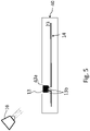
- FIG. 1 it is shown a NFC device 10, in particular in form of a NFC card, which operates as antifraud system according to the solution here described, indicated as a whole with the numerical reference 10.
- a NFC device 10 includes a plastic body 20, having a rectangular shape, which carries an integrated circuit 12, for instance the integrated circuit of a UICC card. Terminals 12a and 12b of the integrated circuit 12 are coupled to an antenna 14 obtained by a metal coil, in particular a track running along the periphery of the plastic body 20.
- the metal track of the antenna 14 starts in particular from the terminal 12a of the integrated circuit 12 and ends in the terminal 12b of the circuit 12, after performing several turns of the periphery of the body 20, in particular in the example three turns, so that, with the exception of where the tracks enter the terminals 12a, 12b, the antenna 14 defines three parallel metal coils co-planar with the plane of the body 20.
- the coils can be of course in a different number, depending on the parameters of the antenna 12.
- a current is generated in the coil of the antenna 14, this current can carry power supply to the integrated circuit 12 for operation.
- the NFC device 10 however includes also a photoresistive circuit, which is a arranged coupled on one of the coils of the antenna 14 and including a photo-resistance 13.
- the photoresistive circuit is configured to increase the resistance of the at least one antenna coil when the at least one photo-resistance is under dark conditions and thus is in its high resistance state.
- the photo-resistance 13 is arranged in series on the coil of the antenna 14, thus when in dark conditions, i.e. the photo-resistance is not reached by the light of a radiation source 16, which can be the sun or ambient lighting, the photo-resistance 13 has high value and increase the total resistance of the antenna 14, decreasing the value of the current generated under an operation threshold of the integrated circuit 12.
- the photo-resistance 13 When exposed to the light photo-resistance 13 has a lower value of resistance, increasing the value of the current generated over the operation threshold of the integrated circuit 12, which can in this way operate normally and can be read by the external reader.
- the photo-resistance 13 disables the electronic circuit 12 when it is not exposed to a light source, i.e. in dark conditions, and assure that no one is able to scan sensible data.
- FIG 2 it is shown a first schematic representation of the manufacturing process, indicated with the reference 100.
- the process includes providing 110 a first transparent plastic overlay sheet 21.
- the first overlay sheet 21 is a plastic transparent layer (PVC, PC, PET or other no conductive material) which operates as support of the structure determining the plastic body 20.
- the process further includes providing 120 a first cover sheet 22which is a preferably opaque plastic sheet, representing the rear side of the card 10.
- the process includes providing 130 a core layer 23, i.e. a layer, preferably a plastic layer, carrying the circuit components, i.e. the integrated circuit 12 connected to the coils of the antenna 14, and, in the example shown, the photo-resistance 13 connected in series on one of the coils for instance the most inner coil of the antenna 14.
- the processes for connecting such components on a plastic substrate are well known to the technicians in the field of Card and e-Passport Manufacturing. Then the process includes providing 140 140 a second cover sheet layer 24 carrying a window 24a, i.e. a hole punched or milled in the sheet 24, which, given a corresponding shape of the core sheet 23 and cover sheet 24, has substantially the same position and size of the photo-resistance 13.
- the second cover sheet layer 24 represents the front sheet of the card on which, for protection, a second transparent plastic sheet 25 is placed.
- a second cover sheet layer 24 carrying a hole 24a having the same position and size of the photo-resistance 13 is provided on the circuit sheet 13.
- the second cover sheet layer 24 represents the front sheet of the card 10: Then the process includes providing 150 a second transparent plastic sheet 2.5.
- All plastic sheets 21-25 in the example are rectangular with the same dimensions. In variant embodiments other shapes of the sheets 21-125 and the antenna 14 may be possible compatibly with the efficiency of the antenna 14. In variant embodiments one or more of the sheets 21-25 can be paper or cardboard sheets.
- the sheets 21-25 are stacked one upon the other, in that order, i.e. on the first transparent layer 21 is placed the first cover sheet 22, then on the first cover sheet 22 is placed the core sheet 23, the on the cover sheet 23 is placed the second cover sheet 23, so that the window 24a frames and contains the photo-resistance 13, finally the second transparent layer 25 is placed on the second cover sheet 24, covering the window 24a with an antiscratch protection which however allows the light reaching the photo-resistance 13 within the window 24a.
- the sheets are shown slightly horizontally shifted for better appreciating the order of the stack, however they have same dimensions and are vertically aligned (see lateral view of figure 3 ), so that when they are assembled together form a single card with the same dimension.
- FIG 3 the stack of figure 2 is shown in a lateral view.
- the sheets are vertically aligned, and the photo-resistance 13 is positioned on the core sheet 23 so that is aligned with the window 24a.
- a recess or, in the example shown, a window 13a obtained by a hole punched in the core sheet 23 is provided, so that the photo-resistance 13 is inserted within said window 13a.
- the body 20 is obtained and the window 13a and 24a are aligned containing the photo-resistance 13, where thickness of said cover sheet 24 summed to the thickness of the core sheet 23 is equal to the thickness, i.e. the vertical dimension, of the photo-resistance 13.
- the lower core sheet 22 can have a corresponding window for the case the photo-resistance has two photosensitive surfaces, upper and lower.
- the manufacturing process of the Near Field Communication device 10 includes basically providing the core sheet 23 carrying at least the integrated circuit 12 and at least one antenna coil 14, then arranging 160 the core sheet 23 within a stack 20aof plastic or paper sheets to form the card support body, laminating 170 said sheet stack 20a to obtain the support body 20, the process comprising also arranging at least a photo-resistance 13 coupled to one of the coils 14 and with at least a photosensitive surface facing outwards from an outer surface of the device support body 20.
- the process can include providing at least a core sheet 23 and a upper 22 and lower 24 cover sheet, the transparent sheets 21 and 25 being used as optional, although preferable, mechanical protection, making the passing window 24a in a vertically corresponding position at least in one of said upper and lower cover sheet 22, 24, and preferably a window 13a in said core sheet 23, arranging said photo-resistance 13 in the window 13a in the core sheet 23 if present or on the core sheet 23, stacking the core sheet 23 between said upper 22 and lower cover sheet 24 inserting the photo-resistance 13 in the window 24a in at least in one of said upper 22 and lower cover sheet to obtain the sheet stack 20a, in particular complete with sheets 21 and 25, laminating said sheet stack 20a to obtain said support body 20.
- this photoresistance may have an upper and a lower photosensitive surface.
- FIG 4 it is shown a variant embodiment of the manufacturing process of figure 3 , which includes providing punched transparent sheets 21, 25 as outer external sheets, and double photosensitive surface.
- a stack 30a includes the core sheet 23, positioned between the cover sheets 22, 24, which have a respective passing window 22a, 24a in correspondence of a photoresistance 13' arranged on the core sheet 23.
- the transparent sheets 21, 25 are placed as outer sheets under sheet 22 and over sheet 24 respectively, and are punched with passing windows 21a, 25a at the same position in the card plane of windows 22a, 24a.
- the photo-resistance 13' has an upper and a lower photosensitive surface, which can be reached from an upper light source 16 and lower light source 16'.
- the transparent overlay 21, 25 assures mechanical/functional performance, usually required for standard ID and financial applications, but does not assure an additional scratch resistance.
- the transparent sheets 21, 25 may not be punched, i.e. without windows 21a, 25a, for instance if the transparence of such sheets 21, 25 is such that it makes negligible the amount of illuminance subtracted from sheets 21,25 from the illuminance reaching the photoresistance 13 or 13'.
- the transparent sheets 21, 25 may be placed directly over the core sheet 23, with or without the windows 21a, 25a.
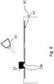
- the process includes providing at least a core sheet 23, stacking at least the core sheet between further layers, which forms the stack 40, laminating said sheet stack 40a to obtain said support body 40, then making a cavity 43a in the card support body 40 reaching said core sheet 23, in particular by a standard milling+embedding process, and arranging said photo-resistance 13 in said cavity 43a on said core sheet 23 electrically connected, by connections 13b, to the coil of antenna 14, in particular by physical soldering or using conductive glue.
- the variant embodiment of figure 5 describes a manufacturing process including providing 120 at least a core sheet 23, stacking 160 at least said core sheet 23 between further sheets, in particular the sheets 21, 22, 24, 25 like in figure 2 , laminating 170 the obtained sheet stack to obtain said support body 40, making a cavity 43a in the device support body 40 reaching said core sheet 23, in particular by a standard milling and embedding process, and arranging said photo-resistance 13 in the cavity 43a on said core sheet 23 electrically connected, by the connections 13b, to said at least one coil, in particular by physical soldering or using conductive glue.
- the variant embodiment of the manufacturing process described with reference to figure 6 includes providing a device support body 50 including a core sheet 23, which is in particular arranged near the surface, arranging said photo-resistance 13 on an outer surface of said support body (50) connected to said at least one coil 14, in particular by physical soldering or using conductive glue, in particular via through-holes in the upper transparent sheet 25.
- Figure 7 it is shown a diagram representing the qualitative characteristic curve of the photoresistance 13, in particular a resistance R13 of the photoresistance 13 as a function of the illuminance E.
- an exemplary value of threshold TH of the illuminance E is shown, having a value around 8 lux, corresponding to a 100 ⁇ resistance of the photoresist 13 which can correspond to dark conditions.
- Typical values of the supply current of a processor in the integrated circuit 12 are below 5 mA, therefore, the photoresistance 13 should be sized so that at the illuminance threshold TH the value of resistance R13 is that the current is below such limit of the supply current of the integrated circuit 12, in particular of its processor, e.g. is below 5 mA.
- the described solution thus provides removing a drawback of contactless solutions using NFC devices, exploiting the fact that while not in use, most NFC device, are in dark conditions, i.e. not reached by the light, thus their NFC device cannot be read until a positive action of exposing to the solar or ambient light is performed by the user. This allows to reject many attempts to fraud, by unauthorizedly reading the NFC device when not in use.
- the photoresistive circuit may include more than one photo-resistance or other light sensitive component, and can be arranged differently with respect to the coil, provided that the circuital arrangement of such photoresistive circuit is configured to increase the resistance of the at least one antenna coil when the at least one photo-resistance is in its high resistance state in dark conditions.
- the Near Field Communication device can be an UICC card or smartcard, or another type of NFC tag. Although most NFC devices are card with a parallelepiped card shape, the Near Field Communication device can have a different structure, like a fob or a keyring, or other structures used for contactless application using NFC.
Landscapes
- Engineering & Computer Science (AREA)
- Computer Hardware Design (AREA)
- Microelectronics & Electronic Packaging (AREA)
- Physics & Mathematics (AREA)
- General Physics & Mathematics (AREA)
- Theoretical Computer Science (AREA)
- Computer Networks & Wireless Communication (AREA)
- Signal Processing (AREA)
- Health & Medical Sciences (AREA)
- Toxicology (AREA)
- General Engineering & Computer Science (AREA)
- Computer Security & Cryptography (AREA)
- Electromagnetism (AREA)
- General Health & Medical Sciences (AREA)
- Artificial Intelligence (AREA)
- Computer Vision & Pattern Recognition (AREA)
- Credit Cards Or The Like (AREA)
- Electrotherapy Devices (AREA)
- Radar Systems Or Details Thereof (AREA)
- Control Of Motors That Do Not Use Commutators (AREA)
Claims (18)
- Nahfeldkommunikationsvorrichtung, umfassend ein Vorrichtungshalterungsgehäuse (20; 30; 40; 50), auf dem mindestens eine Antennenspule (14) angeordnet ist, entlang dem Umfang des Vorrichtungshalterungsgehäuses (20; 30; 40; 50) verlaufend, wobei auf dem Halterungsgehäuse (20; 30; 40; 50) außerdem mindestens eine integrierte Schaltung (12) angeordnet ist, an die mindestens eine Antennenspule (14) gekoppelt, dadurch gekennzeichnet, dass die Nahfeldkommunikationsvorrichtung (10) eine Fotowiderstandsschaltung beinhaltet, durch physikalisches Löten oder Verwenden von leitfähigem Klebstoff gekoppelt an die mindestens eine Antennenspule (14) in Reihe an der Antennenspule (14) angeordnet und mindestens einen Fotowiderstand (13) beinhaltend, wobei die Fotowiderstandsschaltung dazu konfiguriert ist, den Widerstand der mindestens einen Antennenspule (14) zu erhöhen, wenn der mindestens eine Fotowiderstand (13) in seinem hohen Widerstandszustand unter dunklen Bedingungen ist.
- Vorrichtung nach Anspruch 1, dadurch gekennzeichnet, dass das Halterungsgehäuse (20; 30; 40; 50) eine Kernplatte (23) beinhaltet, die integrierte Schaltung (12) und die mindestens eine Antennenspule (14) tragend, die eine Öffnung oder eine Aussparung (13a) beinhaltet, in der der Fotowiderstand (13) montiert ist.
- Vorrichtung nach Anspruch 1 oder 2, dadurch gekennzeichnet, dass das Halterungsgehäuse (20; 30; 40; 50) eine Kernplatte (23) beinhaltet, die integrierte Schaltung (12) und die mindestens eine Antennenspule (14) tragend, wobei die Kernplatte (23) zwischen mindestens einer oberen (22) und einer unteren Platte (24) enthalten ist, wobei die obere und/oder die untere Platte ein Fenster (24a) umfassen, wobei der Fotowiderstand (13) in dem Fenster (24a) montiert ist.
- Vorrichtung nach einem der Ansprüche 1 bis 3, dadurch gekennzeichnet, dass der Fotowiderstand (13) eine obere und eine untere fotoempfindliche Oberfläche beinhaltet.
- Vorrichtung nach einem der vorhergehenden Ansprüche, dadurch gekennzeichnet, dass das Halterungsgehäuse (20; 30; 40; 50) im Wesentlichen ein planares Gehäuse ist.
- Vorrichtung nach einem der vorhergehenden Ansprüche, dadurch gekennzeichnet, dass das Halterungsgehäuse (20; 30; 40; 50) transparente Platten (21, 25) beinhaltet, die seine obere und/oder seine untere äußere Oberfläche bilden.
- Vorrichtung nach einem der vorhergehenden Ansprüche, dadurch gekennzeichnet, dass die Kernplatte (23) eine Durchtrittsöffnung (13a) aufweist und sie zwischen transparenten Platten (21, 25) enthalten ist.
- Vorrichtung nach Anspruch 1, dadurch gekennzeichnet, dass der Fotowiderstand (13) in einer Aushöhlung in dem Halterungsgehäuse angeordnet ist, eine Kernplatte (23) erreichend, die integrierte Schaltung (12) und die mindestens eine Antennenspule (14) tragend.
- Vorrichtung nach Anspruch 1, dadurch gekennzeichnet, dass der Fotowiderstand (13) auf einer äußeren Oberfläche des Halterungsgehäuses (50) angeordnet ist.
- Vorrichtung nach einem der vorhergehenden Ansprüche, dadurch gekennzeichnet, dass eine oder mehrere der Platten (21, 22, 23, 34, 25) Kunststoffplatten oder Papierplatten sind.
- Herstellungsverfahren für eine Nahfeldkommunikationsvorrichtung nach einem der Ansprüche 1 bis 10, umfassend ein Bereitstellen einer Kernplatte (23), mindestens die integrierte Schaltung (12) und die mindestens eine Antennenspule (14) tragend, ein Anordnen der Kernplatte (23) innerhalb eines Stapels (20a; 30a; 40a; 50a) von Kunststoff- oder Papierplatten, um das Kartenhalterungsgehäuse (20; 30; 40; 50) zu bilden, ein Laminieren des Plattenstapels (20a; 30a; 40a; 50a), um das Halterungsgehäuse (20; 30; 40; 50) zu erhalten, wobei das Verfahren außerdem ein Anordnen des mindestens einen Fotowiderstands (13), auf der mindestens eine Spule (14) in Reihe mit der Antennenspule (14) elektrisch verbunden und mit mindestens einer fotoempfindlichen Oberfläche, von einer äußeren Oberfläche des Vorrichtungshalterungsgehäuses (20; 30; 40; 50) nach außen weisend, durch physikalisches Löten oder Verwenden von leitfähigem Klebstoff umfasst;wobei die mindestens eine Antennenspule (14) auf dem Halterungsgehäuse (20; 30; 40; 50) angeordnet wird, entlang dem Umfang des Vorrichtungshalterungsgehäuses (20; 30; 40; 50) verlaufend; undwobei eine Fotowiderstandsschaltung, beinhaltend den mindestens einen Fotowiderstand (13), dazu konfiguriert ist, den Widerstand der mindestens einen Antennenspule (14) zu erhöhen, wenn der mindestens eine Fotowiderstand (13) in seinem hohen Widerstandszustand unter dunklen Bedingungen ist.
- Verfahren nach Anspruch 11, beinhaltend ein Bereitstellen (120, 130, 140) von mindestens einer Kernplatte (23) und einer oberen (22) und einer unteren (24) Deckplatte, ein Herstellen eines Fensters in einer vertikal entsprechenden Position mindestens in einer von der oberen (22) und der unteren Deckplatte (24) und eines Fensters (13a) in der Kernplatte (23), ein Anordnen des Fotowiderstands (13) in dem Fenster (13a) in der Kernplatte (23), ein Stapeln (160) der mindestens einen Kernplatte (23) zwischen der oberen (22) und der unteren Deckplatte (24), ein Einsetzen des Fotowiderstands (13) in das Fenster (24a) mindestens in einer von der oberen (22) und der unteren Deckplatte, um einen Plattenstapel (20a) zu erhalten, ein Laminieren des Plattenstapels (20a), um das Halterungsgehäuse (20) zu erhalten.
- Verfahren nach Anspruch 11, beinhaltend ein Bereitstellen (120) von mindestens einer Kernplatte (23), ein Herstellen eines Fensters (13a) in der Kernplatte (23), ein Anordnen des Fotowiderstands (13') in dem Fenster (13a) in der Kernplatte, wobei der Fotowiderstand (13') eine obere und eine untere fotoempfindliche Oberfläche beinhaltet,
ein Stapeln (160) der mindestens einen Kernplatte in einem Stapel (30a), umfassend eine transparente obere und eine transparente untere Auflageplatte (21, 25), um einen Plattenstapel (30a) zu erhalten, ein Laminieren (170) des Plattenstapels (30a), um das Halterungsgehäuse (30) zu erhalten. - Verfahren nach Anspruch 13, wobei das Stapeln (160) der mindestens einen Kernplatte in einem Stapel (30a) außerdem ein Bereitstellen von einer oberen (22) und einer unteren (24) Deckplatte zwischen der transparenten oberen und der transparenten unteren Auflageplatte (21, 25), ein Herstellen eines Fensters in einer vertikal entsprechenden Position zu dem Fenster (13a) in der Kernplatte (23) mindestens in der oberen (22) und der unteren Deckplatte (24) umfasst.
- Verfahren nach Anspruch 11, beinhaltend ein Bereitstellen (120) von mindestens einer Kernplatte (23), ein Stapeln (160) von mindestens der Kernplatte (23) zwischen weiteren Platten, ein Laminieren (170) des Plattenstapels (40a), um das Halterungsgehäuse (40) zu erhalten, ein Herstellen einer Aushöhlung in dem Vorrichtungshalterungsgehäuses (40), die Kernplatte (23) erreichend, insbesondere durch ein Standardfräs- und - einbettungsverfahren, und ein Anordnen des Fotowiderstands in der Aushöhlung auf der Kernplatte, mit der mindestens einen Spule elektrisch verbunden, insbesondere durch physikalisches Löten oder Verwenden von leitfähigem Klebstoff.
- Verfahren nach Anspruch 11, beinhaltend ein Bereitstellen eines Vorrichtungshalterungsgehäuses (50), beinhaltend eine Kernplatte (23), ein Anordnen des Fotowiderstands (13) auf einer äußeren Oberfläche des Halterungsgehäuses (50), mit der mindestens einen Spule (14) verbunden, insbesondere durch physikalisches Löten oder Verwenden von leitfähigem Klebstoff.
- Verfahren nach einem der vorhergehenden Ansprüche von 11 bis 15, wobei die Dicke der Deckplatte (24) oder von beiden der Deckplatten (22, 24), mit der Dicke der Kernplatte (23) summiert, gleich der Dicke des Fotowiderstands ist.
- Verfahren nach einem der vorhergehenden Ansprüche von 11 bis 17, wobei ein Platzieren einer kratzbeständigen transparenten Auflageplatte (21, 25) auf den äußeren Oberflächen des Stapels (20a, 30a) beinhaltet.
Applications Claiming Priority (1)
| Application Number | Priority Date | Filing Date | Title |
|---|---|---|---|
| IT102018000004051A IT201800004051A1 (it) | 2018-03-28 | 2018-03-28 | Dispositivo di tipo near field communication e corrispondente procedimento di fabbricazione |
Publications (2)
| Publication Number | Publication Date |
|---|---|
| EP3547726A1 EP3547726A1 (de) | 2019-10-02 |
| EP3547726B1 true EP3547726B1 (de) | 2022-05-04 |
Family
ID=62530509
Family Applications (1)
| Application Number | Title | Priority Date | Filing Date |
|---|---|---|---|
| EP19163247.0A Active EP3547726B1 (de) | 2018-03-28 | 2019-03-15 | Nahe feldkommunikationsgeräte und entsprechende fertigungsverfahren |
Country Status (4)
| Country | Link |
|---|---|
| US (1) | US11003973B2 (de) |
| EP (1) | EP3547726B1 (de) |
| CN (2) | CN110321990B (de) |
| IT (1) | IT201800004051A1 (de) |
Families Citing this family (4)
| Publication number | Priority date | Publication date | Assignee | Title |
|---|---|---|---|---|
| IT201800004051A1 (it) * | 2018-03-28 | 2019-09-28 | St Microelectronics Srl | Dispositivo di tipo near field communication e corrispondente procedimento di fabbricazione |
| US10885514B1 (en) * | 2019-07-15 | 2021-01-05 | Capital One Services, Llc | System and method for using image data to trigger contactless card transactions |
| FR3132581B1 (fr) | 2022-02-09 | 2024-10-25 | St Microelectronics Rousset | Dispositif de communication sans contact |
| EP4498283A1 (de) * | 2023-07-24 | 2025-01-29 | HID Global CID SAS | Identifikationsdokument mit aktivierbarem sicherheitsmerkmal |
Family Cites Families (13)
| Publication number | Priority date | Publication date | Assignee | Title |
|---|---|---|---|---|
| US3664244A (en) * | 1970-09-10 | 1972-05-23 | Eastman Kodak Co | Indicating apparatus for exposure control apparatus |
| DE102005039319A1 (de) * | 2005-08-19 | 2007-02-22 | Giesecke & Devrient Gmbh | Kartenförmiger Datenträger |
| US20070040683A1 (en) * | 2005-08-22 | 2007-02-22 | Neal Oliver | Light-activated RFID tag |
| US20080061149A1 (en) * | 2006-09-11 | 2008-03-13 | Colin Tanner | Proximity payment card with security interlock |
| US7561047B2 (en) * | 2006-11-22 | 2009-07-14 | Dai Nippon Printing Co., Ltd. | Noncontact tag and method for producing the same |
| US20120248201A1 (en) * | 2011-01-31 | 2012-10-04 | American Bank Note Company | Dual-interface smart card |
| US9654179B2 (en) * | 2012-03-28 | 2017-05-16 | Xped Holdings Pty Ltd | Method and apparatus for forming associations and communicating between devices |
| CN102663472A (zh) * | 2012-04-17 | 2012-09-12 | 姚学民 | 防止非授权刷卡的非接触射频卡片 |
| US9483723B2 (en) * | 2013-10-06 | 2016-11-01 | Tyfone, Inc. | Passive control secure transaction card |
| US9208424B2 (en) * | 2013-10-06 | 2015-12-08 | Tyfone, Inc. | Active control secure transaction card |
| GB2525869A (en) * | 2014-05-06 | 2015-11-11 | Johnson Electric Sa | Smart card module |
| WO2017066462A1 (en) * | 2015-10-14 | 2017-04-20 | Capital One Services, Llc | Multilayer composite backed card |
| IT201800004051A1 (it) * | 2018-03-28 | 2019-09-28 | St Microelectronics Srl | Dispositivo di tipo near field communication e corrispondente procedimento di fabbricazione |
-
2018
- 2018-03-28 IT IT102018000004051A patent/IT201800004051A1/it unknown
-
2019
- 2019-03-15 EP EP19163247.0A patent/EP3547726B1/de active Active
- 2019-03-27 CN CN201910239978.6A patent/CN110321990B/zh active Active
- 2019-03-27 CN CN201920401181.7U patent/CN209625254U/zh active Active
- 2019-03-28 US US16/368,162 patent/US11003973B2/en active Active
Also Published As
| Publication number | Publication date |
|---|---|
| US11003973B2 (en) | 2021-05-11 |
| CN110321990B (zh) | 2023-08-01 |
| EP3547726A1 (de) | 2019-10-02 |
| CN110321990A (zh) | 2019-10-11 |
| IT201800004051A1 (it) | 2019-09-28 |
| CN209625254U (zh) | 2019-11-12 |
| US20190303736A1 (en) | 2019-10-03 |
Similar Documents
| Publication | Publication Date | Title |
|---|---|---|
| EP3547726B1 (de) | Nahe feldkommunikationsgeräte und entsprechende fertigungsverfahren | |
| RU2470370C1 (ru) | Элемент, содержащий по меньшей мере два микроэлектронных устройства бесконтактного обмена данными | |
| US20240121299A1 (en) | Systems and methods for constructing programmable credential and security cards | |
| US11847518B2 (en) | Systems and methods for constructing programmable credential and security cards | |
| JP5175747B2 (ja) | 有価文書又はセキュリティ書類といった文書及び情報入力方法 | |
| CN100458839C (zh) | 带有应答器的便携式信息载体 | |
| EP3723994B1 (de) | Verbesserte beleuchtbare karte | |
| ES2439942T3 (es) | Documento securizado, especialmente pasaporte electrónico con seguridad reforzada | |
| CA2489152A1 (en) | Wallet card with built-in light | |
| US20250390696A1 (en) | Illuminating transaction card | |
| JP2007510983A (ja) | データキャリア又は文書キャリア | |
| US20080001844A1 (en) | Masking device for contactless portable object in the form of a secure document equipped with a radiofrequency device | |
| JP2006519714A (ja) | ブックカバーインサートとブック型セキュリティ文書、及びブックカバーインサートとブック型セキュリティ文書の製造方法 | |
| WO2018105495A1 (ja) | ヒンジ付積層体、冊子、積層体 | |
| US20240005121A1 (en) | Information-shielding cards and systems and methods for fabricating the same | |
| WO2024246573A1 (en) | A pre-laminated structure with a see-through window and a method of forming it | |
| CN113661500A (zh) | 用于非接触式无源nfc和rfid设备的开关按钮 | |
| CN209879558U (zh) | 带光敏传感器的智能卡 | |
| EP1724711A1 (de) | Positionierungsmittel um ein elektronisches Dokument an die Antenne eines kontaklosen Lesegerät zu halten | |
| KR20240120991A (ko) | 양방향 비접촉식 결제 기능을 가지는 메탈 소재의 rf 디바이스 | |
| RU82052U1 (ru) | Пластиковый носитель бесконтактного типа для доступа к информационным системам | |
| KR200335758Y1 (ko) | 발광기능이 구비된 플라스틱 카드 | |
| CN116888600A (zh) | 用于防护至少一个射频芯片的组件及其制造方法 | |
| KR20120077847A (ko) | 대상물에 인쇄되는 알에프아이디를 갖는 증착필름 및 이를 이용한 보안시스템 | |
| KR20120077848A (ko) | 패턴과와 혼합배치되는 알에프아이디를 갖는 증착필름 및 이를 이용한 보안시스템 |
Legal Events
| Date | Code | Title | Description |
|---|---|---|---|
| PUAI | Public reference made under article 153(3) epc to a published international application that has entered the european phase |
Free format text: ORIGINAL CODE: 0009012 |
|
| STAA | Information on the status of an ep patent application or granted ep patent |
Free format text: STATUS: THE APPLICATION HAS BEEN PUBLISHED |
|
| AK | Designated contracting states |
Kind code of ref document: A1 Designated state(s): AL AT BE BG CH CY CZ DE DK EE ES FI FR GB GR HR HU IE IS IT LI LT LU LV MC MK MT NL NO PL PT RO RS SE SI SK SM TR |
|
| AX | Request for extension of the european patent |
Extension state: BA ME |
|
| STAA | Information on the status of an ep patent application or granted ep patent |
Free format text: STATUS: REQUEST FOR EXAMINATION WAS MADE |
|
| 17P | Request for examination filed |
Effective date: 20200319 |
|
| RBV | Designated contracting states (corrected) |
Designated state(s): AL AT BE BG CH CY CZ DE DK EE ES FI FR GB GR HR HU IE IS IT LI LT LU LV MC MK MT NL NO PL PT RO RS SE SI SK SM TR |
|
| STAA | Information on the status of an ep patent application or granted ep patent |
Free format text: STATUS: EXAMINATION IS IN PROGRESS |
|
| 17Q | First examination report despatched |
Effective date: 20200710 |
|
| GRAP | Despatch of communication of intention to grant a patent |
Free format text: ORIGINAL CODE: EPIDOSNIGR1 |
|
| STAA | Information on the status of an ep patent application or granted ep patent |
Free format text: STATUS: GRANT OF PATENT IS INTENDED |
|
| INTG | Intention to grant announced |
Effective date: 20211122 |
|
| GRAS | Grant fee paid |
Free format text: ORIGINAL CODE: EPIDOSNIGR3 |
|
| GRAA | (expected) grant |
Free format text: ORIGINAL CODE: 0009210 |
|
| STAA | Information on the status of an ep patent application or granted ep patent |
Free format text: STATUS: THE PATENT HAS BEEN GRANTED |
|
| AK | Designated contracting states |
Kind code of ref document: B1 Designated state(s): AL AT BE BG CH CY CZ DE DK EE ES FI FR GB GR HR HU IE IS IT LI LT LU LV MC MK MT NL NO PL PT RO RS SE SI SK SM TR |
|
| REG | Reference to a national code |
Ref country code: GB Ref legal event code: FG4D |
|
| REG | Reference to a national code |
Ref country code: CH Ref legal event code: EP |
|
| REG | Reference to a national code |
Ref country code: AT Ref legal event code: REF Ref document number: 1490442 Country of ref document: AT Kind code of ref document: T Effective date: 20220515 |
|
| REG | Reference to a national code |
Ref country code: DE Ref legal event code: R096 Ref document number: 602019014320 Country of ref document: DE |
|
| REG | Reference to a national code |
Ref country code: IE Ref legal event code: FG4D |
|
| REG | Reference to a national code |
Ref country code: LT Ref legal event code: MG9D |
|
| REG | Reference to a national code |
Ref country code: NL Ref legal event code: MP Effective date: 20220504 |
|
| REG | Reference to a national code |
Ref country code: AT Ref legal event code: MK05 Ref document number: 1490442 Country of ref document: AT Kind code of ref document: T Effective date: 20220504 |
|
| PG25 | Lapsed in a contracting state [announced via postgrant information from national office to epo] |
Ref country code: SE Free format text: LAPSE BECAUSE OF FAILURE TO SUBMIT A TRANSLATION OF THE DESCRIPTION OR TO PAY THE FEE WITHIN THE PRESCRIBED TIME-LIMIT Effective date: 20220504 Ref country code: PT Free format text: LAPSE BECAUSE OF FAILURE TO SUBMIT A TRANSLATION OF THE DESCRIPTION OR TO PAY THE FEE WITHIN THE PRESCRIBED TIME-LIMIT Effective date: 20220905 Ref country code: NO Free format text: LAPSE BECAUSE OF FAILURE TO SUBMIT A TRANSLATION OF THE DESCRIPTION OR TO PAY THE FEE WITHIN THE PRESCRIBED TIME-LIMIT Effective date: 20220804 Ref country code: NL Free format text: LAPSE BECAUSE OF FAILURE TO SUBMIT A TRANSLATION OF THE DESCRIPTION OR TO PAY THE FEE WITHIN THE PRESCRIBED TIME-LIMIT Effective date: 20220504 Ref country code: LT Free format text: LAPSE BECAUSE OF FAILURE TO SUBMIT A TRANSLATION OF THE DESCRIPTION OR TO PAY THE FEE WITHIN THE PRESCRIBED TIME-LIMIT Effective date: 20220504 Ref country code: HR Free format text: LAPSE BECAUSE OF FAILURE TO SUBMIT A TRANSLATION OF THE DESCRIPTION OR TO PAY THE FEE WITHIN THE PRESCRIBED TIME-LIMIT Effective date: 20220504 Ref country code: GR Free format text: LAPSE BECAUSE OF FAILURE TO SUBMIT A TRANSLATION OF THE DESCRIPTION OR TO PAY THE FEE WITHIN THE PRESCRIBED TIME-LIMIT Effective date: 20220805 Ref country code: FI Free format text: LAPSE BECAUSE OF FAILURE TO SUBMIT A TRANSLATION OF THE DESCRIPTION OR TO PAY THE FEE WITHIN THE PRESCRIBED TIME-LIMIT Effective date: 20220504 Ref country code: ES Free format text: LAPSE BECAUSE OF FAILURE TO SUBMIT A TRANSLATION OF THE DESCRIPTION OR TO PAY THE FEE WITHIN THE PRESCRIBED TIME-LIMIT Effective date: 20220504 Ref country code: BG Free format text: LAPSE BECAUSE OF FAILURE TO SUBMIT A TRANSLATION OF THE DESCRIPTION OR TO PAY THE FEE WITHIN THE PRESCRIBED TIME-LIMIT Effective date: 20220804 Ref country code: AT Free format text: LAPSE BECAUSE OF FAILURE TO SUBMIT A TRANSLATION OF THE DESCRIPTION OR TO PAY THE FEE WITHIN THE PRESCRIBED TIME-LIMIT Effective date: 20220504 |
|
| PG25 | Lapsed in a contracting state [announced via postgrant information from national office to epo] |
Ref country code: RS Free format text: LAPSE BECAUSE OF FAILURE TO SUBMIT A TRANSLATION OF THE DESCRIPTION OR TO PAY THE FEE WITHIN THE PRESCRIBED TIME-LIMIT Effective date: 20220504 Ref country code: PL Free format text: LAPSE BECAUSE OF FAILURE TO SUBMIT A TRANSLATION OF THE DESCRIPTION OR TO PAY THE FEE WITHIN THE PRESCRIBED TIME-LIMIT Effective date: 20220504 Ref country code: LV Free format text: LAPSE BECAUSE OF FAILURE TO SUBMIT A TRANSLATION OF THE DESCRIPTION OR TO PAY THE FEE WITHIN THE PRESCRIBED TIME-LIMIT Effective date: 20220504 Ref country code: IS Free format text: LAPSE BECAUSE OF FAILURE TO SUBMIT A TRANSLATION OF THE DESCRIPTION OR TO PAY THE FEE WITHIN THE PRESCRIBED TIME-LIMIT Effective date: 20220904 |
|
| PG25 | Lapsed in a contracting state [announced via postgrant information from national office to epo] |
Ref country code: SM Free format text: LAPSE BECAUSE OF FAILURE TO SUBMIT A TRANSLATION OF THE DESCRIPTION OR TO PAY THE FEE WITHIN THE PRESCRIBED TIME-LIMIT Effective date: 20220504 Ref country code: SK Free format text: LAPSE BECAUSE OF FAILURE TO SUBMIT A TRANSLATION OF THE DESCRIPTION OR TO PAY THE FEE WITHIN THE PRESCRIBED TIME-LIMIT Effective date: 20220504 Ref country code: RO Free format text: LAPSE BECAUSE OF FAILURE TO SUBMIT A TRANSLATION OF THE DESCRIPTION OR TO PAY THE FEE WITHIN THE PRESCRIBED TIME-LIMIT Effective date: 20220504 Ref country code: EE Free format text: LAPSE BECAUSE OF FAILURE TO SUBMIT A TRANSLATION OF THE DESCRIPTION OR TO PAY THE FEE WITHIN THE PRESCRIBED TIME-LIMIT Effective date: 20220504 Ref country code: DK Free format text: LAPSE BECAUSE OF FAILURE TO SUBMIT A TRANSLATION OF THE DESCRIPTION OR TO PAY THE FEE WITHIN THE PRESCRIBED TIME-LIMIT Effective date: 20220504 Ref country code: CZ Free format text: LAPSE BECAUSE OF FAILURE TO SUBMIT A TRANSLATION OF THE DESCRIPTION OR TO PAY THE FEE WITHIN THE PRESCRIBED TIME-LIMIT Effective date: 20220504 |
|
| REG | Reference to a national code |
Ref country code: DE Ref legal event code: R097 Ref document number: 602019014320 Country of ref document: DE |
|
| PLBE | No opposition filed within time limit |
Free format text: ORIGINAL CODE: 0009261 |
|
| STAA | Information on the status of an ep patent application or granted ep patent |
Free format text: STATUS: NO OPPOSITION FILED WITHIN TIME LIMIT |
|
| PG25 | Lapsed in a contracting state [announced via postgrant information from national office to epo] |
Ref country code: AL Free format text: LAPSE BECAUSE OF FAILURE TO SUBMIT A TRANSLATION OF THE DESCRIPTION OR TO PAY THE FEE WITHIN THE PRESCRIBED TIME-LIMIT Effective date: 20220504 |
|
| 26N | No opposition filed |
Effective date: 20230207 |
|
| PG25 | Lapsed in a contracting state [announced via postgrant information from national office to epo] |
Ref country code: SI Free format text: LAPSE BECAUSE OF FAILURE TO SUBMIT A TRANSLATION OF THE DESCRIPTION OR TO PAY THE FEE WITHIN THE PRESCRIBED TIME-LIMIT Effective date: 20220504 |
|
| PG25 | Lapsed in a contracting state [announced via postgrant information from national office to epo] |
Ref country code: MC Free format text: LAPSE BECAUSE OF FAILURE TO SUBMIT A TRANSLATION OF THE DESCRIPTION OR TO PAY THE FEE WITHIN THE PRESCRIBED TIME-LIMIT Effective date: 20220504 |
|
| REG | Reference to a national code |
Ref country code: CH Ref legal event code: PL |
|
| GBPC | Gb: european patent ceased through non-payment of renewal fee |
Effective date: 20230315 |
|
| REG | Reference to a national code |
Ref country code: BE Ref legal event code: MM Effective date: 20230331 |
|
| PG25 | Lapsed in a contracting state [announced via postgrant information from national office to epo] |
Ref country code: LU Free format text: LAPSE BECAUSE OF NON-PAYMENT OF DUE FEES Effective date: 20230315 |
|
| REG | Reference to a national code |
Ref country code: IE Ref legal event code: MM4A |
|
| PG25 | Lapsed in a contracting state [announced via postgrant information from national office to epo] |
Ref country code: GB Free format text: LAPSE BECAUSE OF NON-PAYMENT OF DUE FEES Effective date: 20230315 |
|
| PG25 | Lapsed in a contracting state [announced via postgrant information from national office to epo] |
Ref country code: LI Free format text: LAPSE BECAUSE OF NON-PAYMENT OF DUE FEES Effective date: 20230331 Ref country code: IT Free format text: LAPSE BECAUSE OF FAILURE TO SUBMIT A TRANSLATION OF THE DESCRIPTION OR TO PAY THE FEE WITHIN THE PRESCRIBED TIME-LIMIT Effective date: 20220504 Ref country code: IE Free format text: LAPSE BECAUSE OF NON-PAYMENT OF DUE FEES Effective date: 20230315 Ref country code: GB Free format text: LAPSE BECAUSE OF NON-PAYMENT OF DUE FEES Effective date: 20230315 Ref country code: FR Free format text: LAPSE BECAUSE OF NON-PAYMENT OF DUE FEES Effective date: 20230331 Ref country code: CH Free format text: LAPSE BECAUSE OF NON-PAYMENT OF DUE FEES Effective date: 20230331 |
|
| PG25 | Lapsed in a contracting state [announced via postgrant information from national office to epo] |
Ref country code: BE Free format text: LAPSE BECAUSE OF NON-PAYMENT OF DUE FEES Effective date: 20230331 |
|
| PG25 | Lapsed in a contracting state [announced via postgrant information from national office to epo] |
Ref country code: BG Free format text: LAPSE BECAUSE OF FAILURE TO SUBMIT A TRANSLATION OF THE DESCRIPTION OR TO PAY THE FEE WITHIN THE PRESCRIBED TIME-LIMIT Effective date: 20220504 |
|
| PG25 | Lapsed in a contracting state [announced via postgrant information from national office to epo] |
Ref country code: BG Free format text: LAPSE BECAUSE OF FAILURE TO SUBMIT A TRANSLATION OF THE DESCRIPTION OR TO PAY THE FEE WITHIN THE PRESCRIBED TIME-LIMIT Effective date: 20220504 |
|
| PGFP | Annual fee paid to national office [announced via postgrant information from national office to epo] |
Ref country code: DE Payment date: 20250218 Year of fee payment: 7 |
|
| PG25 | Lapsed in a contracting state [announced via postgrant information from national office to epo] |
Ref country code: CY Free format text: LAPSE BECAUSE OF FAILURE TO SUBMIT A TRANSLATION OF THE DESCRIPTION OR TO PAY THE FEE WITHIN THE PRESCRIBED TIME-LIMIT; INVALID AB INITIO Effective date: 20190315 |
|
| PG25 | Lapsed in a contracting state [announced via postgrant information from national office to epo] |
Ref country code: HU Free format text: LAPSE BECAUSE OF FAILURE TO SUBMIT A TRANSLATION OF THE DESCRIPTION OR TO PAY THE FEE WITHIN THE PRESCRIBED TIME-LIMIT; INVALID AB INITIO Effective date: 20190315 |
|
| PG25 | Lapsed in a contracting state [announced via postgrant information from national office to epo] |
Ref country code: TR Free format text: LAPSE BECAUSE OF FAILURE TO SUBMIT A TRANSLATION OF THE DESCRIPTION OR TO PAY THE FEE WITHIN THE PRESCRIBED TIME-LIMIT Effective date: 20220504 |