EP3540804A1 - Photoelectric conversion element, imaging element and imaging device - Google Patents
Photoelectric conversion element, imaging element and imaging device Download PDFInfo
- Publication number
- EP3540804A1 EP3540804A1 EP17870234.6A EP17870234A EP3540804A1 EP 3540804 A1 EP3540804 A1 EP 3540804A1 EP 17870234 A EP17870234 A EP 17870234A EP 3540804 A1 EP3540804 A1 EP 3540804A1
- Authority
- EP
- European Patent Office
- Prior art keywords
- group
- substituted
- photoelectric conversion
- organic compound
- unsubstituted
- Prior art date
- Legal status (The legal status is an assumption and is not a legal conclusion. Google has not performed a legal analysis and makes no representation as to the accuracy of the status listed.)
- Granted
Links
Images





Classifications
-
- H—ELECTRICITY
- H10—SEMICONDUCTOR DEVICES; ELECTRIC SOLID-STATE DEVICES NOT OTHERWISE PROVIDED FOR
- H10K—ORGANIC ELECTRIC SOLID-STATE DEVICES
- H10K85/00—Organic materials used in the body or electrodes of devices covered by this subclass
- H10K85/60—Organic compounds having low molecular weight
- H10K85/649—Aromatic compounds comprising a hetero atom
- H10K85/655—Aromatic compounds comprising a hetero atom comprising only sulfur as heteroatom
-
- H—ELECTRICITY
- H04—ELECTRIC COMMUNICATION TECHNIQUE
- H04N—PICTORIAL COMMUNICATION, e.g. TELEVISION
- H04N25/00—Circuitry of solid-state image sensors [SSIS]; Control thereof
- H04N25/60—Noise processing, e.g. detecting, correcting, reducing or removing noise
- H04N25/63—Noise processing, e.g. detecting, correcting, reducing or removing noise applied to dark current
-
- H—ELECTRICITY
- H10—SEMICONDUCTOR DEVICES; ELECTRIC SOLID-STATE DEVICES NOT OTHERWISE PROVIDED FOR
- H10F—INORGANIC SEMICONDUCTOR DEVICES SENSITIVE TO INFRARED RADIATION, LIGHT, ELECTROMAGNETIC RADIATION OF SHORTER WAVELENGTH OR CORPUSCULAR RADIATION
- H10F30/00—Individual radiation-sensitive semiconductor devices in which radiation controls the flow of current through the devices, e.g. photodetectors
- H10F30/20—Individual radiation-sensitive semiconductor devices in which radiation controls the flow of current through the devices, e.g. photodetectors the devices having potential barriers, e.g. phototransistors
- H10F30/21—Individual radiation-sensitive semiconductor devices in which radiation controls the flow of current through the devices, e.g. photodetectors the devices having potential barriers, e.g. phototransistors the devices being sensitive to infrared, visible or ultraviolet radiation
- H10F30/22—Individual radiation-sensitive semiconductor devices in which radiation controls the flow of current through the devices, e.g. photodetectors the devices having potential barriers, e.g. phototransistors the devices being sensitive to infrared, visible or ultraviolet radiation the devices having only one potential barrier, e.g. photodiodes
- H10F30/223—Individual radiation-sensitive semiconductor devices in which radiation controls the flow of current through the devices, e.g. photodetectors the devices having potential barriers, e.g. phototransistors the devices being sensitive to infrared, visible or ultraviolet radiation the devices having only one potential barrier, e.g. photodiodes the potential barrier being a PIN barrier
-
- H—ELECTRICITY
- H10—SEMICONDUCTOR DEVICES; ELECTRIC SOLID-STATE DEVICES NOT OTHERWISE PROVIDED FOR
- H10F—INORGANIC SEMICONDUCTOR DEVICES SENSITIVE TO INFRARED RADIATION, LIGHT, ELECTROMAGNETIC RADIATION OF SHORTER WAVELENGTH OR CORPUSCULAR RADIATION
- H10F39/00—Integrated devices, or assemblies of multiple devices, comprising at least one element covered by group H10F30/00, e.g. radiation detectors comprising photodiode arrays
- H10F39/10—Integrated devices
- H10F39/12—Image sensors
-
- H—ELECTRICITY
- H10—SEMICONDUCTOR DEVICES; ELECTRIC SOLID-STATE DEVICES NOT OTHERWISE PROVIDED FOR
- H10K—ORGANIC ELECTRIC SOLID-STATE DEVICES
- H10K30/00—Organic devices sensitive to infrared radiation, light, electromagnetic radiation of shorter wavelength or corpuscular radiation
-
- H—ELECTRICITY
- H10—SEMICONDUCTOR DEVICES; ELECTRIC SOLID-STATE DEVICES NOT OTHERWISE PROVIDED FOR
- H10K—ORGANIC ELECTRIC SOLID-STATE DEVICES
- H10K30/00—Organic devices sensitive to infrared radiation, light, electromagnetic radiation of shorter wavelength or corpuscular radiation
- H10K30/20—Organic devices sensitive to infrared radiation, light, electromagnetic radiation of shorter wavelength or corpuscular radiation comprising organic-organic junctions, e.g. donor-acceptor junctions
-
- H—ELECTRICITY
- H10—SEMICONDUCTOR DEVICES; ELECTRIC SOLID-STATE DEVICES NOT OTHERWISE PROVIDED FOR
- H10K—ORGANIC ELECTRIC SOLID-STATE DEVICES
- H10K39/00—Integrated devices, or assemblies of multiple devices, comprising at least one organic radiation-sensitive element covered by group H10K30/00
-
- H—ELECTRICITY
- H10—SEMICONDUCTOR DEVICES; ELECTRIC SOLID-STATE DEVICES NOT OTHERWISE PROVIDED FOR
- H10K—ORGANIC ELECTRIC SOLID-STATE DEVICES
- H10K85/00—Organic materials used in the body or electrodes of devices covered by this subclass
- H10K85/30—Coordination compounds
- H10K85/311—Phthalocyanine
-
- H—ELECTRICITY
- H10—SEMICONDUCTOR DEVICES; ELECTRIC SOLID-STATE DEVICES NOT OTHERWISE PROVIDED FOR
- H10K—ORGANIC ELECTRIC SOLID-STATE DEVICES
- H10K85/00—Organic materials used in the body or electrodes of devices covered by this subclass
- H10K85/60—Organic compounds having low molecular weight
- H10K85/631—Amine compounds having at least two aryl rest on at least one amine-nitrogen atom, e.g. triphenylamine
- H10K85/636—Amine compounds having at least two aryl rest on at least one amine-nitrogen atom, e.g. triphenylamine comprising heteroaromatic hydrocarbons as substituents on the nitrogen atom
-
- H—ELECTRICITY
- H10—SEMICONDUCTOR DEVICES; ELECTRIC SOLID-STATE DEVICES NOT OTHERWISE PROVIDED FOR
- H10K—ORGANIC ELECTRIC SOLID-STATE DEVICES
- H10K99/00—Subject matter not provided for in other groups of this subclass
-
- H—ELECTRICITY
- H10—SEMICONDUCTOR DEVICES; ELECTRIC SOLID-STATE DEVICES NOT OTHERWISE PROVIDED FOR
- H10K—ORGANIC ELECTRIC SOLID-STATE DEVICES
- H10K2101/00—Properties of the organic materials covered by group H10K85/00
- H10K2101/30—Highest occupied molecular orbital [HOMO], lowest unoccupied molecular orbital [LUMO] or Fermi energy values
-
- H—ELECTRICITY
- H10—SEMICONDUCTOR DEVICES; ELECTRIC SOLID-STATE DEVICES NOT OTHERWISE PROVIDED FOR
- H10K—ORGANIC ELECTRIC SOLID-STATE DEVICES
- H10K30/00—Organic devices sensitive to infrared radiation, light, electromagnetic radiation of shorter wavelength or corpuscular radiation
- H10K30/30—Organic devices sensitive to infrared radiation, light, electromagnetic radiation of shorter wavelength or corpuscular radiation comprising bulk heterojunctions, e.g. interpenetrating networks of donor and acceptor material domains
-
- H—ELECTRICITY
- H10—SEMICONDUCTOR DEVICES; ELECTRIC SOLID-STATE DEVICES NOT OTHERWISE PROVIDED FOR
- H10K—ORGANIC ELECTRIC SOLID-STATE DEVICES
- H10K39/00—Integrated devices, or assemblies of multiple devices, comprising at least one organic radiation-sensitive element covered by group H10K30/00
- H10K39/30—Devices controlled by radiation
- H10K39/32—Organic image sensors
-
- H—ELECTRICITY
- H10—SEMICONDUCTOR DEVICES; ELECTRIC SOLID-STATE DEVICES NOT OTHERWISE PROVIDED FOR
- H10K—ORGANIC ELECTRIC SOLID-STATE DEVICES
- H10K85/00—Organic materials used in the body or electrodes of devices covered by this subclass
- H10K85/30—Coordination compounds
- H10K85/321—Metal complexes comprising a group IIIA element, e.g. Tris (8-hydroxyquinoline) gallium [Gaq3]
-
- H—ELECTRICITY
- H10—SEMICONDUCTOR DEVICES; ELECTRIC SOLID-STATE DEVICES NOT OTHERWISE PROVIDED FOR
- H10K—ORGANIC ELECTRIC SOLID-STATE DEVICES
- H10K85/00—Organic materials used in the body or electrodes of devices covered by this subclass
- H10K85/30—Coordination compounds
- H10K85/331—Metal complexes comprising an iron-series metal, e.g. Fe, Co, Ni
-
- H—ELECTRICITY
- H10—SEMICONDUCTOR DEVICES; ELECTRIC SOLID-STATE DEVICES NOT OTHERWISE PROVIDED FOR
- H10K—ORGANIC ELECTRIC SOLID-STATE DEVICES
- H10K85/00—Organic materials used in the body or electrodes of devices covered by this subclass
- H10K85/30—Coordination compounds
- H10K85/341—Transition metal complexes, e.g. Ru(II)polypyridine complexes
- H10K85/342—Transition metal complexes, e.g. Ru(II)polypyridine complexes comprising iridium
-
- H—ELECTRICITY
- H10—SEMICONDUCTOR DEVICES; ELECTRIC SOLID-STATE DEVICES NOT OTHERWISE PROVIDED FOR
- H10K—ORGANIC ELECTRIC SOLID-STATE DEVICES
- H10K85/00—Organic materials used in the body or electrodes of devices covered by this subclass
- H10K85/30—Coordination compounds
- H10K85/341—Transition metal complexes, e.g. Ru(II)polypyridine complexes
- H10K85/346—Transition metal complexes, e.g. Ru(II)polypyridine complexes comprising platinum
-
- H—ELECTRICITY
- H10—SEMICONDUCTOR DEVICES; ELECTRIC SOLID-STATE DEVICES NOT OTHERWISE PROVIDED FOR
- H10K—ORGANIC ELECTRIC SOLID-STATE DEVICES
- H10K85/00—Organic materials used in the body or electrodes of devices covered by this subclass
- H10K85/60—Organic compounds having low molecular weight
- H10K85/615—Polycyclic condensed aromatic hydrocarbons, e.g. anthracene
- H10K85/622—Polycyclic condensed aromatic hydrocarbons, e.g. anthracene containing four rings, e.g. pyrene
-
- H—ELECTRICITY
- H10—SEMICONDUCTOR DEVICES; ELECTRIC SOLID-STATE DEVICES NOT OTHERWISE PROVIDED FOR
- H10K—ORGANIC ELECTRIC SOLID-STATE DEVICES
- H10K85/00—Organic materials used in the body or electrodes of devices covered by this subclass
- H10K85/60—Organic compounds having low molecular weight
- H10K85/615—Polycyclic condensed aromatic hydrocarbons, e.g. anthracene
- H10K85/623—Polycyclic condensed aromatic hydrocarbons, e.g. anthracene containing five rings, e.g. pentacene
-
- H—ELECTRICITY
- H10—SEMICONDUCTOR DEVICES; ELECTRIC SOLID-STATE DEVICES NOT OTHERWISE PROVIDED FOR
- H10K—ORGANIC ELECTRIC SOLID-STATE DEVICES
- H10K85/00—Organic materials used in the body or electrodes of devices covered by this subclass
- H10K85/60—Organic compounds having low molecular weight
- H10K85/615—Polycyclic condensed aromatic hydrocarbons, e.g. anthracene
- H10K85/624—Polycyclic condensed aromatic hydrocarbons, e.g. anthracene containing six or more rings
-
- H—ELECTRICITY
- H10—SEMICONDUCTOR DEVICES; ELECTRIC SOLID-STATE DEVICES NOT OTHERWISE PROVIDED FOR
- H10K—ORGANIC ELECTRIC SOLID-STATE DEVICES
- H10K85/00—Organic materials used in the body or electrodes of devices covered by this subclass
- H10K85/60—Organic compounds having low molecular weight
- H10K85/631—Amine compounds having at least two aryl rest on at least one amine-nitrogen atom, e.g. triphenylamine
- H10K85/633—Amine compounds having at least two aryl rest on at least one amine-nitrogen atom, e.g. triphenylamine comprising polycyclic condensed aromatic hydrocarbons as substituents on the nitrogen atom
-
- Y—GENERAL TAGGING OF NEW TECHNOLOGICAL DEVELOPMENTS; GENERAL TAGGING OF CROSS-SECTIONAL TECHNOLOGIES SPANNING OVER SEVERAL SECTIONS OF THE IPC; TECHNICAL SUBJECTS COVERED BY FORMER USPC CROSS-REFERENCE ART COLLECTIONS [XRACs] AND DIGESTS
- Y02—TECHNOLOGIES OR APPLICATIONS FOR MITIGATION OR ADAPTATION AGAINST CLIMATE CHANGE
- Y02E—REDUCTION OF GREENHOUSE GAS [GHG] EMISSIONS, RELATED TO ENERGY GENERATION, TRANSMISSION OR DISTRIBUTION
- Y02E10/00—Energy generation through renewable energy sources
- Y02E10/50—Photovoltaic [PV] energy
- Y02E10/549—Organic PV cells
Definitions
- the present invention relates to a photoelectric conversion element, an image pickup element, and an image pickup apparatus.
- PTL 1 describes an organic photoelectric conversion element, in which an electron-blocking layer is disposed between a photoelectric conversion layer and an anode and in which dark current is reduced by specifying an energy level relationship between the photoelectric conversion layer and the electron-blocking layer and by specifying the layer thickness of the electron-blocking layer.
- PTL 2 describes an organic photoelectric conversion element, in which a hole-blocking layer is disposed between a photoelectric conversion layer and a cathode and in which dark current is reduced by specifying an energy level relationship between the photoelectric conversion layer and the hole-blocking layer.
- the dark current in the photoelectric conversion element includes dark current generated in the photoelectric conversion layer in addition to current that flows from the anode and from the cathode.
- PTLs 1 and 2 neither describe nor indicate dark current that is generated between a p-type organic semiconductor material and an n-type organic semiconductor material in the photoelectric conversion layer. Therefore, a reduction in dark current in the photoelectric conversion element is insufficient.
- an object of the present invention to provide an organic photoelectric conversion element in which dark current that is generated between a p-type organic semiconductor material and an n-type organic semiconductor material in a photoelectric conversion layer in a photoelectric conversion element is reduced.
- a photoelectric conversion element including an anode, a cathode, and a photoelectric conversion layer disposed between the anode and the cathode
- the photoelectric conversion layer contains a first organic compound and a second organic compound
- the oxidation potential of the first organic compound is lower than the oxidation potential of the second organic compound
- ⁇ E denoted by formula (A) below satisfies formula (B) below
- ⁇ ⁇ E oxidation potential of first organic compound ⁇ reduction potential of second organic compound ⁇ ⁇ E ⁇ 1.5 V
- the first organic compound is denoted by any one of general formulae [1] to [5] below.
- R 1 represents a hydrogen atom, a halogen atom, a substituted or unsubstituted alkyl group, a substituted or unsubstituted alkoxy group, a substituted or unsubstituted aryl group, a substituted or unsubstituted heterocyclic group, a substituted or unsubstituted vinyl group, a substituted or unsubstituted amino group, or a cyano group.
- Each of n 1 and n 2 represents an integer of 0 to 4, each of X 1 to X 3 represents a nitrogen atom, a sulfur atom, an oxygen atom, or a carbon atom that may have a substituent.
- Each of Ar 1 and Ar 2 is selected from a substituted or unsubstituted aryl group and a substituted or unsubstituted heterocyclic group.
- Ar 1 When a plurality of symbols Ar 1 are included, these may be the same or different from each other, when a plurality of symbols Ar 2 are included, these may be the same or different from each other, and when X 2 or X 3 is a carbon atom, Ar 1 and Ar 2 may form a ring by bonding to each other.
- Z 1 represents a halogen atom, a cyano group, a substituted or unsubstituted heteroaryl group, or any substituent denoted by general formulae [1-1] to [1-9] below.
- each of R 521 to R 588 is selected from a hydrogen atom, a halogen atom, a substituted or unsubstituted alkyl group, a substituted or unsubstituted alkoxy group, a substituted or unsubstituted aryl group, a substituted or unsubstituted heterocyclic group, a substituted or unsubstituted vinyl group, a substituted or unsubstituted amino group, and a cyano group.
- each of R 20 to R 29 is selected from a hydrogen atom, a halogen atom, a substituted or unsubstituted alkyl group, a substituted or unsubstituted alkoxy group, a substituted or unsubstituted aryl group, a substituted or unsubstituted heterocyclic group, a substituted or unsubstituted vinyl group, a substituted or unsubstituted amino group, and a cyano group.
- Two of R 20 to R 29 may form a ring by bonding to each other.
- Each of L 1 to L 9 represents a ligand that coordinates with the metal M.
- the ligand is composed of a substituted or unsubstituted aryl group or a substituted or unsubstituted heterocyclic group, and two of L 1 to L 9 , the two being adjacent to each other, may form a ring by bonding to each other.
- a photoelectric conversion element including an anode, a cathode, and a photoelectric conversion layer disposed between the anode and the cathode is provided, wherein the activation energy of dark current is 0.70 eV or more.
- a photoelectric conversion element in which dark current is reduced can be provided.
- the present invention relates to a reduction in dark current in a photoelectric conversion element including a photoelectric conversion layer composed of an organic compound. Dark current can be reduced by increasing an energy difference between two types of organic compounds contained in the photoelectric conversion layer to a specific value or more.
- the activation energy is the magnitude of energy required for exciting the first organic compound and the second organic compound to a charge separation state.
- Application of energy higher than or equal to the activation energy by the thermal energy causes dark current.
- dark current in a photoelectric conversion element is reduced by setting the activation energy of dark current to be 0.70 eV or more.
- the activation energy of dark current is preferably 0.75 eV or more and further preferably 0.80 eV or more.
- a photoelectric conversion element including a photoelectric conversion layer composed of an organic compound between an anode and a cathode will be described as an example.
- the photoelectric conversion layer included in the photoelectric conversion element according to the present invention is a layer that receives light so as to generate electric charge in accordance with the amount of the light.
- the function of the photoelectric conversion layer is to perform charge separation into holes and electrons on the basis of light absorption so as to convert the light into electric signals.
- the photoelectric conversion layer may contain a plurality of types of organic compounds.
- a layer in which a donor material that carries positive charge into the photoelectric conversion layer and an acceptor material that carries negative charge are mixed at random is called a bulk heterojunction.
- Fig. 1 is an energy diagram showing ⁇ E.
- the oxidation potential of the first organic compound corresponds to HOMO of the first organic compound.
- the reduction potential of the second organic compound corresponds to LUMO of the second organic compound.
- the oxidation-reduction potential is a potential energy difference between molecules in a solution and an electrode and is a physical property value of the molecule alone.
- Dark current may be generated from a p-type organic semiconductor material to an n-type organic semiconductor material due to thermal charge separation.
- ⁇ E is energy necessary for generation of dark current due to thermal charge separation.
- the activation energy can be increased and dark current can be reduced by the photoelectric conversion layer including an organic compound that is suppressed from coming into contact with other molecules or an organic compound that suppresses generation of thermal electrons.
- the photoelectric conversion element according to the present embodiment is a photoelectric conversion element in which dark current is reduced because the photoelectric conversion layer contains the first organic compound and the second organic compound, the first organic compound has a property of suppressing contact with other molecules or a property of suppressing generation of thermal electrons.
- the first organic compound is the p-type organic semiconductor contained in the photoelectric conversion layer.
- the first organic compound is an organic semiconductor with donor ability and has a property of readily providing electrons.
- the first organic compound is an organic compound having a lower oxidation potential. That is, the first organic compound is an electron donor material, and the second organic compound is an electron acceptor material.
- Examples of compounds usable as the first organic compound include a triarylamine compound, a pyran compound, a quinacridone compound, a benzidine compound, a pyrazoline compound, a styrylamine compound, a hydrazone compound, a triphenylmethane compound, a carbazole compound, a polysilane compound, a thiophene compound, a phthalocyanine compound, a cyanine compound, a merocyanine compound, an oxonol compound, a polyamine compound, an indole compound, a pyrrole compound, a pyrazole compound, a polyarylene compound, a fused aromatic carbon ring compound (a naphthalene derivative, an anthracene derivative, a phenanthrene derivative, a tetracene derivative, a pyrene derivative, a perylene derivative, and a fluoranthene derivative), and a metal complex including a nitrogen-containing
- the fluoranthene derivative is a compound with a chemical structural formula having a fluoranthene skeleton.
- a compound in which a fused ring is added to the fluoranthene skeleton is also included. That is, a compound in which the fluoranthene skeleton is present in the chemical structural formula is referred to as the fluoranthene derivative.
- the absorption peak wavelength can be obtained by, for example, measuring an absorption spectrum in a chloroform solution.
- the absorption peak wavelength of the first organic compound is 530 nm or more
- formula (B) be satisfied and the activation energy of dark current be set to be a specific value or more.
- An organic compound having an absorption peak wavelength of 530 nm or more is an organic compound having a relatively small band gap.
- HOMO thereof tends to approach LUMO of the second organic compound. That is, dark current is readily generated. In this case, great effect is exerted by satisfying formula (B) or satisfying that the activation energy of dark current is set to be a specific value or more.
- the concentration of the first organic compound in the photoelectric conversion layer is preferably less than 35% by weight, where the total of the first organic compound and the second organic compound is assumed to be 100% by weight, and 27.5% by weight or less is more preferable. It is favorable that the concentration of the first organic compound be within the preferable range because dark current can be further reduced.
- the first organic compound is denoted by any one of general formulae [1] to [5] below. It is particularly preferable that the first organic compound be an organic compound denoted by general formula [1].
- n 1 and n 2 represents an integer of 0 to 4.
- Each of X 1 to X 3 represents a nitrogen atom, a sulfur atom, an oxygen atom, or a carbon atom that may have a substituent.
- Each of Ar 1 and Ar 2 is selected from a substituted or unsubstituted aryl group and a substituted or unsubstituted heterocyclic group.
- Ar 1 When a plurality of symbols Ar 1 are included, these may be the same or different from each other, when a plurality of symbols Ar 2 are included, these may be the same or different from each other, and when X 2 or X 3 is a carbon atom, Ar 1 and Ar 2 may form a ring by bonding to each other.
- Z 1 represents a halogen atom, a cyano group, a substituted or unsubstituted heteroaryl group, or any substituent denoted by general formulae [1-1] to [1-9] below.
- each of R 521 to R 588 is selected from a hydrogen atom, a halogen atom, a substituted or unsubstituted alkyl group, a substituted or unsubstituted alkoxy group, a substituted or unsubstituted aryl group, a substituted or unsubstituted heterocyclic group, a substituted or unsubstituted vinyl group, a substituted or unsubstituted amino group, and a cyano group.
- Ar 1 be a substituted or unsubstituted aryl group or a substituted or unsubstituted heterocyclic group.
- the heteroatom in the heterocyclic group is nitrogen.
- X 1 is a sulfur atom or an oxygen atom.
- n 1 is 1 and n 2 is 0. Since n 2 is 0, Ar 2 represents a single bond.
- the first organic compound may be denoted by general formula [2] below.
- each of R 20 to R 29 is selected from a hydrogen atom, a halogen atom, a substituted or unsubstituted alkyl group, a substituted or unsubstituted alkoxy group, a substituted or unsubstituted aryl group, a substituted or unsubstituted heterocyclic group, a substituted or unsubstituted vinyl group, a substituted or unsubstituted amino group, and a cyano group.
- Two of R 20 to R 29 may form a ring by bonding to each other.
- the first organic compound may be denoted by any one of general formulae [3] to [5] below.
- general formula [2] may be represented by any one of general formulae [11] to [27] below.
- each of R 31 to R 390 is selected from a hydrogen atom, a halogen atom, a substituted or unsubstituted alkyl group, a substituted or unsubstituted alkoxy group, a substituted or unsubstituted aryl group, a substituted or unsubstituted heterocyclic group, a substituted or unsubstituted vinyl group, a substituted or unsubstituted amino group, and a cyano group.
- the halogen atom is a chlorine atom, a bromine atom, or an iodine atom, and a fluorine atom is preferable.
- the alkoxy group is preferably an alkoxy group having a carbon atom number of 1 to 10. Examples include a methoxy group, an ethoxy group, a normal propoxy group, an isopropoxy group, a normal butoxy group, a tertiary butoxy group, a secondary butoxy group, and an octoxy group.
- the alkoxy group may be an alkoxy group having a carbon atom number of 1 to 4.
- the aryl group is preferably an aryl group having a carbon atom number of 6 to 20.
- Examples include a phenyl group, a naphthyl group, an indenyl group, a biphenyl group, a terphenyl group, a fluorenyl group, an anthrathenyl group, a pyrenyl group, a fluoranthenyl group, and a perylenyl group.
- a phenyl group, a biphenyl group, a terphenyl group, a fluorenyl group, and a naphthyl group are preferable in consideration of low molecular weight and sublimability of the compound.
- the heterocyclic group is preferably a heterocyclic group having a carbon atom number of 3 to 15.
- Examples include a pyridyl group, a pyrazyl group, a triazyl group, a thienyl group, a furanyl group, a pyrrolyl group, an oxazolyl group, an oxadiazolyl group, a thiazolyl group, a thiadiazolyl group, a carbazolyl group, an acridinyl group, a phenanthrolyl group, a benzothiophenyl group, a dibenzothiophenyl group, a benzothiazolyl group, a benzoazolyl group, and a benzopyrrolyl group.
- a heteroatom included in the heterocyclic group is preferably nitrogen.
- the amino group is preferably an amino group having an alkyl group or an aryl group as a substituent.
- Examples include an N-methylamino group, an N,N-dimethylamino group, an N,N-diethylamino group, an N-methyl-N-ethylamino group, an N-benzylamino group, an N-methyl-N-benzylamino group, an N,N-dibenzylamino group, an anilino group, an N,N-diphenylamino group, an N,N-dinaphthylamino group, an N,N-difluorenylamino group, an N-phenyl-N-tolylamino group, an N,N-ditolylamino group, an N-methyl-N-phenylamino group, an N,N-dianisolylamino group, an N-mesityl-N-phenylamino group, an N,N-dimesity
- substituents examples include an alkyl group having a carbon atom number of 1 to 4, for example, a methyl group, an ethyl group, a propyl group, and a butyl group, an aralkyl group, for example, a benzyl group, an aryl group, for example, a phenyl group and a biphenyl group, a heterocyclic group in which a heteroatom is a nitrogen atom, for example, a pyridyl group and a pyrrolyl group, an amino group, for example, a dimethylamino group, a diethylamino group, a dibenzylamino group, a diphenylamino group, and a ditolylamino group, an alkoxy group, for example, a methoxy group, an ethoxy group, a propoxy group, and a phenoxy group, a cyclic ketone group, for example, a 1,3-indaned
- ligands L 1 to L 9 in general formulae [3] to [5] are as described below.
- the ligands L 1 to L 9 are ligands in which a plurality of substituents selected from substituted or unsubstituted aryl groups and substituted or unsubstituted heterocyclic groups are bonded.
- aryl group constituting the ligand examples include a phenyl group, a naphthyl group, an indenyl group, a biphenyl group, a terphenyl group, a fluorenyl group, an anthrathenyl group, a pyrenyl group, a fluoranthenyl group, and a perylenyl group but are not limited to these, as a matter of course.
- heterocyclic group constituting the ligand examples include a pyridyl group, a pyrazyl group, a triazyl group, a thienyl group, a furanyl group, a pyrrolyl group, an oxazolyl group, an oxadiazolyl group, a thiazolyl group, a thiadiazolyl group, a carbazolyl group, an acridinyl group, a phenanthrolyl group, a benzothiophenyl group, a dibenzothiophenyl group, a benzothiazolyl group, a benzoazolyl group, and a benzopyrrolyl group but are not limited to these.
- Examples of the substituent included in the ligand in general formulae [3] to [5], that is, the substituent included in the aryl group or the heterocyclic group include an alkyl group having a carbon atom number of 1 to 4, for example, a methyl group, an ethyl group, a propyl group, and a butyl group, an aralkyl group, for example, a benzyl group, an aryl group, for example, a phenyl group and a biphenyl group, a heterocyclic group in which a heteroatom is a nitrogen atom, for example, a pyridyl group and a pyrrolyl group, an amino group, for example, a dimethylamino group, a diethylamino group, a dibenzylamino group, a diphenylamino group, and a ditolylamino group, an alkoxy group, for example, a methoxy group, an ethoxy group
- the ligand may have a hydroxy group, a carboxy group, or the like as a substituent and may be metal-atom-bonded by interposing the hydroxy group or the carboxy group.
- general formula [1] have a structure denoted by general formula [28] below.
- Each of R 391 to R 396 is selected from a hydrogen atom, a halogen atom, a substituted or unsubstituted alkyl group, a substituted or unsubstituted alkoxy group, a substituted or unsubstituted aryl group, a substituted or unsubstituted heterocyclic group, a substituted or unsubstituted vinyl group, a substituted or unsubstituted amino group, and a cyano group.
- Two of R 391 to R 396 may form a ring by bonding to each other.
- R 394 and R 395 form a ring by bonding to each other.
- Exemplary examples 1-1 to 1-24 are a group of compounds having a sulfur-atom-containing five-membered heterocyclic group at the center.
- the compound which has the heterocyclic group and in which Z 1 is an electron-withdrawing substituent is a compound having a low HOMO level. As a result, ⁇ E can be increased, and generation of thermal electrons that cause dark current is suppressed.
- an organic compound having Ar 1 or Ar 2 has a large excluded volume and, therefore, has a low probability of contact with other molecules. Consequently, an acceptor material does not readily approach, and transfer of electrons due to thermal excitation does not readily occur. As a result, dark current can be reduced.
- Exemplary examples 2-1 to 2-56 are a group of compounds having a fluoranthene skeleton at the center.
- the fluoranthene skeleton has an electron-withdrawing property and, therefore, is preferable first organic compound because generation of thermal electrons that cause dark current is suppressed.
- Exemplary examples 3-1 to 3-14 are a group of complex compounds containing a metal atom at the center.
- Each ligand contains a heterocyclic compound as a section having an electron-withdrawing property and, thereby, generation of thermal electrons that cause dark current is suppressed. Consequently, these complex compounds are preferable as the first organic compound.
- the first organic compound has an oxidation potential of preferably 0.65 V or more.
- the photoelectric conversion layer may contain fullerene or a fullerene derivative as the second organic compound.
- the fullerene or fullerene derivative may function as an n-type organic semiconductor.
- An electron transport path is formed by molecules of fullerene or a fullerene derivative being connected to each other in the photoelectric conversion layer. Consequently, an electron transport property is improved, and high-speed responsiveness of the photoelectric conversion element is improved.
- the content of fullerene or a fullerene derivative may be 40% by weight or more and 85% by weight or less, where the total of the first organic compound and the second organic compound is assumed to be 100% by weight, in consideration of photoelectric conversion efficiency.
- fullerene or fullerene derivative examples include fullerene C60, fullerene C70, fullerene C76, fullerene C78, fullerene C80, fullerene C82, fullerene C84, fullerene C90, fullerene C96, fullerene C240, fullerene 540, mixed fullerene, and fullerene nanotube.
- the fullerene derivative may have a substituent.
- substituents include an alkyl group, an aryl group, and a heterocyclic group.
- the photoelectric conversion element according to the present invention may further include a hole-blocking layer between the anode and the photoelectric conversion layer.
- the hole-blocking layer is a layer that suppresses flowing of holes from the anode into the photoelectric conversion layer, and it is preferable that the ionization potential be high.
- the photoelectric conversion element according to the present invention may further include an electron-blocking layer between the cathode and the photoelectric conversion layer.
- the electron-blocking layer is a layer that suppresses flowing of electrons from the cathode into the photoelectric conversion layer, and it is preferable that the electron affinity or LUMO (lowest unoccupied molecular orbital energy) be low.
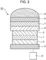
- Fig. 2 is a schematic sectional view showing an example of a photoelectric conversion element according to the present embodiment.
- a photoelectric conversion layer 1 that converts light to electric charge is disposed between an anode 4 and a cathode 5 that are a pair of electrodes.
- a protective layer 7, a wavelength selection portion 8, and a microlens 9 are disposed on the anode.
- a reading circuit 6 is connected to the cathode.
- the material for constituting the electrode include a metal, a metal oxide, a metal nitride, a metal boride, and an organic conductive compound and mixtures of these.
- Further specific examples include a conductive metal oxide, for example, tin oxide doped with antimony, fluorine, or the like (ATO, FTO), tin oxide, zinc oxide, indium oxide, indium tin oxide (ITO), or indium zinc oxide (IZO), a metal, for example, gold, silver, chromium, nickel, titanium, tungsten, or aluminum, a conductive compound, for example, an oxide, a nitride, or the like of these metals (titanium nitride (TiN) is an example), a mixture or a layered material of these metals and a conductive metal oxide, an inorganic conductive substance, for example, copper iodide or copper sulfide, an organic conductive material, for example, a polyaniline, a polythi
- the hole or electron collection electrode included in the photoelectric conversion element according to the present invention is an electrode that collects holes or electrons of the charge generated in the photoelectric conversion layer.
- the collection electrode located at a lower portion may be a pixel electrode in the configuration of an image pickup element. Whether the pixel electrode is a cathode or an anode is determined in accordance with an element configuration or a circuit configuration of a groundwork.
- the order may be substrate/anode/photoelectric conversion layer/cathode on the substrate, or the order may be substrate/cathode/photoelectric conversion layer/anode.
- a method for forming the electrode may be appropriately selected in consideration of suitability for the electrode material. Specifically, formation may be performed by a wet system, for example, a printing system or a coating system, a physical system, for example, a vacuum evaporation method, a sputtering method, or an ion plating method, a chemical system, for example, CVD or a plasma CVD method, or the like.
- a wet system for example, a printing system or a coating system
- a physical system for example, a vacuum evaporation method, a sputtering method, or an ion plating method
- a chemical system for example, CVD or a plasma CVD method, or the like.
- a thin film sealing layer there is no particular limitation regarding a thin film sealing layer, and an inorganic material is used for formation.
- Specific examples include silicon oxide, silicon nitride, silicon oxynitride, and aluminum oxide.
- Silicon oxide, silicon nitride, and silicon oxynitride may be formed by a sputtering method or a CVD method.
- Aluminum oxide may be formed by an ALD method (atomic layer deposition method).
- the thin film sealing layer having a smaller thickness is preferable because an effect of reducing color mixing is enhanced as the distance from a photoelectric conversion layer to a color filter decreases in the case of use as an image pickup element.
- An image pickup element includes a plurality of pixels, and each of the pixels includes a photoelectric conversion element according to the present invention and a reading transistor connected to the photoelectric conversion element.
- the plurality of pixels are arranged in the matrix with a plurality of rows and a plurality of columns.
- Each pixel may be connected to a signal processing circuit.
- the signal processing circuit can obtain an image by receiving a signal from each pixel.
- the signal processing circuit may be a CMOS sensor or a CCD sensor.
- the image pickup element may include an optical filter, for example, a color filter.
- a color filter in accordance with the photoelectric conversion element be included.
- one color filter may be disposed for one light-receiving pixel, or one color filter may be disposed for a plurality of light-receiving pixels.
- optical filter examples include, in addition to the color filter, a low-pass filter that transmits wavelengths of infrared rays or higher and a UV cut filter that transmits wavelengths of ultraviolet rays or lower.
- the image pickup element may include an optical member, for example, a microlens.
- the microlens is a lens that condenses light from outside on a photoelectric conversion portion.
- each light-receiving pixel may include one microlens, or one microlens may be disposed so as to address a plurality of light-receiving pixels. In the case in which a plurality of light-receiving pixels are disposed, it is preferable that each of the plurality of light-receiving pixels include one microlens.
- the image pickup apparatus may include a receiving portion that receives a signal from outside.
- the signal received by the receiving portion is a signal that can control at least one of an image pickup range, start of image pickup, and finish of image pickup of the image pickup apparatus.
- the image pickup apparatus may further includes a sending portion that sends an acquired image to outside. Examples of the acquired image include a picked-up image and an image sent from another device.
- a pixel 18 may include the photoelectric conversion element 10 and a reading circuit that reads a signal generated in the photoelectric conversion portion.
- the reading circuit may include, for example, a transfer transistor 11 electrically connected to the photoelectric conversion element, an amplifying transistor 13 including a gate electrode electrically connected to the photoelectric conversion element 10, a selection transistor 14 that selects a pixel from which information is read, and a reset transistor 12 that supplies a reset voltage to the photoelectric conversion element.
- Transfer of the transfer transistor 11 may be controlled by pTX.
- Supply of the voltage to the reset transistor may be controlled by pRES.
- the selection transistor is set to be in the state of selection or non-selection by pSEL.
- the transfer transistor 11, the reset transistor 12, and the amplifying transistor 13 are connected to each other at node B. It is possible to include no transfer transistor in accordance with the configuration.
- the reset transistor is a transistor that supplies a voltage to reset the potential at node B. Supply of the voltage can be controlled by applying pRES to the gate of the reset transistor. It is possible to include no reset transistor in accordance with the configuration.
- the amplifying transistor is a transistor that passes a current in accordance with the potential at node B.
- the amplifying transistor is connected to the selection transistor 14 that selects a pixel from which a signal is output.
- the selection transistor is connected to a current source 16 and a column output portion 15, and the column output portion 15 may be connected to a signal processing portion.
- the selection transistor 14 is connected to a vertical output signal line 17.
- the vertical output signal line 17 is connected to the current source 16 and the column output portion 15.
- Fig. 4 is a diagram showing an image pickup element according to the present invention.
- the image pickup element 20 includes an image pickup region 25 in which a plurality of pixels are two-dimensionally arranged and a peripheral region 26. A region other than the image pickup region is the peripheral region.
- the peripheral region includes a vertical scanning circuit 21, a reading circuit 22, a horizontal scanning circuit 23, and an output amplifier 24, and the output amplifier is connected to a signal processing portion 27.
- the signal processing portion is a signal processing portion that performs signal processing based on the information read by the reading circuit, and examples include a CCD circuit and a CMOS circuit.
- the reading circuit 22 includes, for example, a column amplifier, a CDS circuit, an adding circuit, and the like and performs amplification, addition, and the like relative to signals read through the vertical signal line from pixels in the row selected by the vertical scanning circuit 21.
- the column amplifier, the CDS circuit, the adding circuit, and the like are arranged, for example, on a pixel column or a plurality of pixel columns basis.
- the horizontal scanning circuit 23 generates signals for sequentially reading signals of the reading circuit 22.
- the output amplifier 24 amplifies and outputs signals of a row selected by the horizontal scanning circuit 23.
- the above-described configuration is just a configuration example of the photoelectric conversion apparatus, and the present embodiment is not limited to this.
- one each of the reading circuit 22, the horizontal scanning circuit 23, and the output amplifier 24 is arranged on and under the image pickup region 25.
- three or more output paths may be disposed. Signals output from output amplifiers are combined as an image signal in the signal processing portion.
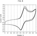
- Electrochemical characteristics for example, an oxidation potential, can be evaluated by cyclic voltammetry (CV) .
- a CV measurement sample was prepared by dissolving about 1 mg of first organic compound into 10 mL of 0.1-M ortho-dichlorobenzene solution of tetrabutylammonium perchlorate and performing deaeration treatment using nitrogen.
- a three-electrode method was used for the CV measurement.
- a nonaqueous-solvent-based Ag/Ag + reference electrode, a platinum counter electrode having a diameter of 0.5 mm and a length of 5 cm, and a glassy carbon working electrode having an inner diameter of 3 mm (every electrode was produced by BAS Inc.) were used.
- An electrochemical analyzer Model 660C produced by ALS Co., Ltd. was used as an electrochemical measurement apparatus.
- Fig. 5 is a diagram showing an example of a cyclic voltammogram that determines the oxidation potential and the reduction potential of an organic compound.
- the oxidation potential and the reduction potential can be assumed from a peak value of the cyclic voltammogram.
- the oxidation potential is referred to as Eox and the reduction potential is referred to as Ered.
- Table 1 shows the oxidation potentials of exemplary compounds of the first organic compound.
- a photoelectric conversion element was produced by using a combination of a first organic compound and a second organic compound, where ⁇ E ⁇ 1.5 V applied. Dark current was measured by using the resulting photoelectric conversion element.
- the photoelectric conversion element was formed on a Si substrate.
- a cathode, an electron-blocking layer, a photoelectric conversion layer, a hole-blocking layer, and an anode were sequentially formed.
- the Si substrate was prepared, in which a wiring layer and an insulating layer were stacked and, for the purpose of enabling communication, contact holes were disposed from the wiring layer through the insulating layer at a place corresponding to each pixel by forming an opening. This contact hole is connected to a pad portion at a substrate edge by a conductive line.
- An IZO electrode was formed by a sputtering method so as to overlap the contact hole portion. Patterning was performed so as to form 3 mm 2 of IZO electrode (cathode). At this time, the film thickness of the IZO electrode was set to be 100 nm.
- An organic compound layer was formed on the IZO electrode by a vacuum evaporation method.
- the layer configuration and the layer thickness were as shown in Table 2 below.
- IZO serving as an anode was formed by a sputtering method.
- the thickness of the anode was set to be 30 nm.
- the layer configuration of the photoelectric conversion element is shown in Table 2.
- compound (d-1) As the electron-blocking layer, compound (d-1) below was used.
- any one of exemplary compounds 1-1 to 3-14 was used.
- any one of fullerene C60 (d-2), fullerene C70 (d-3), and organic compound (d-4) below was used.
- the photoelectric conversion element was held in a constant temperature bath at 60°C and the measurement was performed by bringing a prober wired to a semiconductor parameter analyzer (4155C, Agilent Technologies, Inc.) into contact with an electrode.
- a semiconductor parameter analyzer (4155C, Agilent Technologies, Inc.
- a to C were rated as good, and D and E were rated as poor.
- Photoelectric conversion elements were produced in the same manner as example 1 except that the combination of the first organic compound and the second organic compound was changed to a combination shown in Table 4.
- the results of examples 1 to 47 are shown in Table 4 below.
- Photoelectric conversion elements were produced in the same manner as example 1 except that the combination of the first organic compound and the second organic compound was changed to a combination shown in Table 5.
- the combination of compounds shown in Table 5 was a combination where ⁇ E ⁇ 1.5 V applied.
- the resulting photoelectric conversion element was subjected to the dark current evaluation in the same measuring method as example 1.
- the concentration of the first organic compound is preferably less than 35% by weight and more preferably 27.5% by weight or less.
- the lower limit concentration is not limited by the present invention and may be, for example, a concentration at which necessary absorptance is obtained.
- Photoelectric conversion elements were produced in the same manner as example 1 except that the constituent material and the layer thickness were set to be as shown in Table 7.
- the exemplary compound shown in Table 8 or comparative compound (e-1) below was used but is expressed as "first organic compound” in Table 7.
- the dark current of each element was measured and relative evaluation was performed.
- the structure of comparative compound (e-1) was as described below.
- the oxidation potential of compound e-1 was 0.92 V.
- the maximum absorption peak wavelength refers to the wavelength of a peak having the greatest absorption coefficient.
- a chloroform solution in which the first organic compound was mol/L was produced, and the absorption spectrum was measured by a spectrophotometer (JASCO Corporation Ubest-550). The maximum absorption peak wavelength and the absorbance were determined on the basis of the measurement results.
- the molar absorptivity was determined from the absorbance in accordance with Lambert-Beer law.
- the compound denoted by general formula [28] can obtain an absorption peak suitable for obtaining a panchromatic absorption band in the visible range and strong absorption with molar absorptivity of 40,000 or more. Strong absorption is associated with a high external quantum yield and, therefore, is important factor for the photoelectric conversion element.
- a photoelectric conversion element was produced in the same manner as example 1 except that a silicon nitride layer by using a CVD method was used as the sealing layer.
- the silicon nitride layer having a layer thickness of 1 ⁇ m was formed.
- Durability was evaluated by irradiating the resulting element with LED light of 365 nm at intensity of 1 W/cm 2 for 24 h.
- the absorptance of the LED light of 365 nm by the resulting SiN (1 ⁇ m) was 75%.
- the value of dark current in this element did not change even after a lapse of 24 h.
- the dark current about 10% increased after light irradiation for 24 hours. This is because the glass cap has lower ultraviolet absorptance than SiN.
- the sealing layer be formed of a material that can absorb ultraviolet rays.
- Fig. 6 is a diagram showing the Arrhenius plot of the photoelectric conversion element in example 1.
- the vertical axis indicates the dark current value normalized by the dark current value at 60°C.
- the vertical axis is graduated in common logarithms.
- the horizontal axis indicates the reciprocal of absolute temperature.
- the absolute value of the gradient increases as the temperature increases from about 60°C.
- the activation energy was determined from this gradient on the basis of formula (5) below.
- T absolute temperature
- k B Boltzmann constant
- E a activation energy
- J current value at temperature T
- J 0 a frequency factor.
- the dark current activation energy determined from the gradient was 0.84 eV.
- the activation energy was determined in the same method as example 55 and was plotted relative to corresponding ⁇ E as shown in Fig. 7 . It is shown that the activation energy tends to increase as ⁇ E increases. As is clear from Fig. 7 , when ⁇ E is 1.5 V or more, the activation energy is high. This indicates that when ⁇ E is 1.5 V or more, a probability of charge generation due to thermal excitation is reduced. In this regard, Table 10 shows the relationship between the activation energy and the dark current evaluation. As shown in Table 10, when the activation energy is 0.70 eV or more, the rating of dark current is C or better.
- the photoelectric conversion element according to the present invention is a photoelectric conversion element in which dark current is reduced.
- An image pickup element including the photoelectric conversion element is preferable because dark current noise resulting from the photoelectric conversion element portion is at a low level.
Landscapes
- Engineering & Computer Science (AREA)
- Physics & Mathematics (AREA)
- Chemical & Material Sciences (AREA)
- Materials Engineering (AREA)
- Spectroscopy & Molecular Physics (AREA)
- Electromagnetism (AREA)
- Signal Processing (AREA)
- Multimedia (AREA)
- Inorganic Chemistry (AREA)
- Light Receiving Elements (AREA)
- Solid State Image Pick-Up Elements (AREA)
- Organic Low-Molecular-Weight Compounds And Preparation Thereof (AREA)
- Transforming Light Signals Into Electric Signals (AREA)
- Electroluminescent Light Sources (AREA)
Abstract
Description
- The present invention relates to a photoelectric conversion element, an image pickup element, and an image pickup apparatus.
- In recent years, development of a solid state image pickup element having a structure in which an organic compound is used for a photoelectric conversion layer disposed on a signal-reading substrate has advanced.
- Various configurations for improving dark current in a photoelectric conversion element are known.
PTL 1 describes an organic photoelectric conversion element, in which an electron-blocking layer is disposed between a photoelectric conversion layer and an anode and in which dark current is reduced by specifying an energy level relationship between the photoelectric conversion layer and the electron-blocking layer and by specifying the layer thickness of the electron-blocking layer. -
PTL 2 describes an organic photoelectric conversion element, in which a hole-blocking layer is disposed between a photoelectric conversion layer and a cathode and in which dark current is reduced by specifying an energy level relationship between the photoelectric conversion layer and the hole-blocking layer. - The dark current in the photoelectric conversion element includes dark current generated in the photoelectric conversion layer in addition to current that flows from the anode and from the cathode.
-
PTLs - Accordingly, it is an object of the present invention to provide an organic photoelectric conversion element in which dark current that is generated between a p-type organic semiconductor material and an n-type organic semiconductor material in a photoelectric conversion layer in a photoelectric conversion element is reduced.
-
- PTL 1: Japanese Patent Laid-Open No.
2010-183060 - PTL 2: Japanese Patent Laid-Open No.
2007-088033 - According to an aspect of the present invention, a photoelectric conversion element including an anode, a cathode, and a photoelectric conversion layer disposed between the anode and the cathode is provided, wherein the photoelectric conversion layer contains a first organic compound and a second organic compound, the oxidation potential of the first organic compound is lower than the oxidation potential of the second organic compound, ΔE denoted by formula (A) below satisfies formula (B) below,



- In general formula [1], R1 represents a hydrogen atom, a halogen atom, a substituted or unsubstituted alkyl group, a substituted or unsubstituted alkoxy group, a substituted or unsubstituted aryl group, a substituted or unsubstituted heterocyclic group, a substituted or unsubstituted vinyl group, a substituted or unsubstituted amino group, or a cyano group.
- Each of n1 and n2 represents an integer of 0 to 4, each of X1 to X3 represents a nitrogen atom, a sulfur atom, an oxygen atom, or a carbon atom that may have a substituent.
- Each of Ar1 and Ar2 is selected from a substituted or unsubstituted aryl group and a substituted or unsubstituted heterocyclic group.
- When a plurality of symbols Ar1 are included, these may be the same or different from each other, when a plurality of symbols Ar2 are included, these may be the same or different from each other, and when X2 or X3 is a carbon atom, Ar1 and Ar2 may form a ring by bonding to each other.
- Z1 represents a halogen atom, a cyano group, a substituted or unsubstituted heteroaryl group, or any substituent denoted by general formulae [1-1] to [1-9] below.
- In general formulae [1-1] to [1-9], each of R521 to R588 is selected from a hydrogen atom, a halogen atom, a substituted or unsubstituted alkyl group, a substituted or unsubstituted alkoxy group, a substituted or unsubstituted aryl group, a substituted or unsubstituted heterocyclic group, a substituted or unsubstituted vinyl group, a substituted or unsubstituted amino group, and a cyano group.


- In general formula [2], each of R20 to R29 is selected from a hydrogen atom, a halogen atom, a substituted or unsubstituted alkyl group, a substituted or unsubstituted alkoxy group, a substituted or unsubstituted aryl group, a substituted or unsubstituted heterocyclic group, a substituted or unsubstituted vinyl group, a substituted or unsubstituted amino group, and a cyano group. Two of R20 to R29, the two being adjacent to each other, may form a ring by bonding to each other.

- In general formulae [3] to [5], M represents a metal atom. The metal atom may have an oxygen atom or a halogen atom as a substituent.
- Each of L1 to L9 represents a ligand that coordinates with the metal M. The ligand is composed of a substituted or unsubstituted aryl group or a substituted or unsubstituted heterocyclic group, and two of L1 to L9, the two being adjacent to each other, may form a ring by bonding to each other.
- In addition, according to another aspect of the present invention, a photoelectric conversion element including an anode, a cathode, and a photoelectric conversion layer disposed between the anode and the cathode is provided, wherein the activation energy of dark current is 0.70 eV or more.
- According to the present invention, a photoelectric conversion element in which dark current is reduced can be provided.
-
-
Fig. 1 is an energy diagram showing ΔE according to the present invention. -
Fig. 2 is a schematic sectional view showing an example of a photoelectric conversion element according to the present invention. -
Fig. 3 is a diagram showing an example of a circuit that drives a pixel including a photoelectric conversion element according to the present invention. -
Fig. 4 is a schematic diagram showing an example of a peripheral circuit of an image pickup element including a photoelectric conversion element according to the present invention. -
Fig. 5 is a diagram showing an example of a cyclic voltammogram that determines the oxidation potential and the reduction potential of an organic compound. -
Fig. 6 is a diagram showing the Arrhenius plot of dark current values of a photoelectric conversion element containing an organic compound according to the present invention. -
Fig. 7 is a diagram showing the relationship between the activation energy (Ea) of dark current in a photoelectric conversion element using an exemplary compound and ΔE of the photoelectric conversion element. Description of Embodiments - The present invention relates to a reduction in dark current in a photoelectric conversion element including a photoelectric conversion layer composed of an organic compound. Dark current can be reduced by increasing an energy difference between two types of organic compounds contained in the photoelectric conversion layer to a specific value or more.
- Meanwhile, the dark current can be reduced by setting the activation energy of dark current in the photoelectric conversion element to be a specific value or more.
- Dark current due to thermal charge separation is not readily generated when the activation energy increases. The activation energy is the magnitude of energy required for exciting the first organic compound and the second organic compound to a charge separation state. Application of energy higher than or equal to the activation energy by the thermal energy causes dark current.
- According to an aspect of the present invention, dark current in a photoelectric conversion element is reduced by setting the activation energy of dark current to be 0.70 eV or more. The activation energy of dark current is preferably 0.75 eV or more and further preferably 0.80 eV or more.
- In the present embodiment, a photoelectric conversion element including a photoelectric conversion layer composed of an organic compound between an anode and a cathode will be described as an example.
- The photoelectric conversion layer included in the photoelectric conversion element according to the present invention is a layer that receives light so as to generate electric charge in accordance with the amount of the light. The function of the photoelectric conversion layer is to perform charge separation into holes and electrons on the basis of light absorption so as to convert the light into electric signals. The photoelectric conversion layer may contain a plurality of types of organic compounds. A layer in which a donor material that carries positive charge into the photoelectric conversion layer and an acceptor material that carries negative charge are mixed at random is called a bulk heterojunction.
- When the photoelectric conversion layer contains a plurality of types of organic compounds, the plurality of types of organic compounds may be mixed in one layer, or the plurality of types of organic compounds may be contained in a plurality of layers.
- It is preferable that the photoelectric conversion layer be a layer containing a p-type organic semiconductor or an n-type organic semiconductor. It is more preferable that bulk heterolayers in which an organic p-type compound and an organic n-type compound are mixed be included in at least some of the photoelectric conversion layers. In other words, the heterolayer may be a mixed layer.
- The photoelectric conversion layer including the bulk heterolayer has high photoelectric conversion efficiency. Further, in the bulk heterolayer having an appropriate mixing ratio, the electron mobility and the hole mobility are high in the photoelectric conversion layer, and the optical response speed of the photoelectric conversion element is high. Therefore, it is preferable that a bulk heterolayer having an optimum mixing ratio be included.
- ΔE is an energy gap defined by formula (A) below.


-
Fig. 1 is an energy diagram showing ΔE. The oxidation potential of the first organic compound corresponds to HOMO of the first organic compound. Meanwhile, the reduction potential of the second organic compound corresponds to LUMO of the second organic compound. The oxidation-reduction potential is a potential energy difference between molecules in a solution and an electrode and is a physical property value of the molecule alone. - Dark current may be generated from a p-type organic semiconductor material to an n-type organic semiconductor material due to thermal charge separation. In a sense, ΔE is energy necessary for generation of dark current due to thermal charge separation.
- When formula (B) is satisfied, generation of dark current due to thermal excitation rather than optical excitation can be suppressed.
- This is because the magnitude of ΔE correlates with the activation energy of dark current generation and, more specifically, the activation energy of the dark current tends to increase when ΔE increases. When formula (B) is satisfied, the activation energy of dark current generation is increased, generation of dark current due to thermal excitation is suppressed, and thereby a photoelectric conversion element in which dark current is reduced can be obtained.
- Meanwhile, dark current due to thermal excitation is caused by contact between molecules of a p-type organic semiconductor and molecules of an n-type organic semiconductor, which form a bulk heterojunction.
- In addition to formula (B), the activation energy can be increased and dark current can be reduced by the photoelectric conversion layer including an organic compound that is suppressed from coming into contact with other molecules or an organic compound that suppresses generation of thermal electrons.
- The photoelectric conversion element according to the present embodiment is a photoelectric conversion element in which dark current is reduced because the photoelectric conversion layer contains the first organic compound and the second organic compound, the first organic compound has a property of suppressing contact with other molecules or a property of suppressing generation of thermal electrons.
- The photoelectric conversion layer contains the first organic compound and the second organic compound, and the first organic compound is an electron donor material.
- The first organic compound is the p-type organic semiconductor contained in the photoelectric conversion layer. The first organic compound is an organic semiconductor with donor ability and has a property of readily providing electrons. Specifically, of the two organic compounds, the first organic compound is an organic compound having a lower oxidation potential. That is, the first organic compound is an electron donor material, and the second organic compound is an electron acceptor material.
- Examples of compounds usable as the first organic compound include a triarylamine compound, a pyran compound, a quinacridone compound, a benzidine compound, a pyrazoline compound, a styrylamine compound, a hydrazone compound, a triphenylmethane compound, a carbazole compound, a polysilane compound, a thiophene compound, a phthalocyanine compound, a cyanine compound, a merocyanine compound, an oxonol compound, a polyamine compound, an indole compound, a pyrrole compound, a pyrazole compound, a polyarylene compound, a fused aromatic carbon ring compound (a naphthalene derivative, an anthracene derivative, a phenanthrene derivative, a tetracene derivative, a pyrene derivative, a perylene derivative, and a fluoranthene derivative), and a metal complex including a nitrogen-containing heterocyclic compound as a ligand. In particular, a triarylamine compound, a pyran compound, a quinacridone compound, a pyrrole compound, a phthalocyanine compound, a merocyanine compound, and a fussed aromatic carbon ring compound are preferable.
- The fluoranthene derivative is a compound with a chemical structural formula having a fluoranthene skeleton. A compound in which a fused ring is added to the fluoranthene skeleton is also included. That is, a compound in which the fluoranthene skeleton is present in the chemical structural formula is referred to as the fluoranthene derivative. The same applies to other derivatives, that is, the naphthalene derivative, the anthracene derivative, the phenanthrene derivative, the tetracene derivative, the pyrene derivative, and the perylene derivative.
- The first organic compound is preferably within a visible range with an absorption wavelength of 450 nm or more and 700 nm or less. For the purpose of providing the photoelectric conversion layer with a panchromatic absorption band, the absorption peak wavelength is preferably 500 nm or more. In particular, 530 nm or more is preferable, and 530 nm or more and 650 nm or less is further preferable. When the absorption peak wavelength falls within the above-described range, absorption also occurs in a blue range of 450 nm or more and 470 nm or less and a red range of 600 nm or more and 630 nm or less, which are nearby ranges, and as a result, panchromatism is improved.
- The absorption peak wavelength can be obtained by, for example, measuring an absorption spectrum in a chloroform solution.
- In this regard, when the absorption peak wavelength of the first organic compound is 530 nm or more, it is particularly preferable that formula (B) be satisfied and the activation energy of dark current be set to be a specific value or more.
- An organic compound having an absorption peak wavelength of 530 nm or more is an organic compound having a relatively small band gap. Regarding the organic compound having a small band gap, HOMO thereof tends to approach LUMO of the second organic compound. That is, dark current is readily generated. In this case, great effect is exerted by satisfying formula (B) or satisfying that the activation energy of dark current is set to be a specific value or more.
- The concentration of the first organic compound in the photoelectric conversion layer is preferably less than 35% by weight, where the total of the first organic compound and the second organic compound is assumed to be 100% by weight, and 27.5% by weight or less is more preferable. It is favorable that the concentration of the first organic compound be within the preferable range because dark current can be further reduced.
- The first organic compound is denoted by any one of general formulae [1] to [5] below. It is particularly preferable that the first organic compound be an organic compound denoted by general formula [1].

- In general formula [1], R1 represents a hydrogen atom, a halogen atom, a substituted or unsubstituted alkyl group, a substituted or unsubstituted alkoxy group, a substituted or unsubstituted aryl group, a substituted or unsubstituted heterocyclic group, a substituted or unsubstituted vinyl group, a substituted or unsubstituted amino group, or a cyano group.
- Each of n1 and n2 represents an integer of 0 to 4.
- Each of X1 to X3 represents a nitrogen atom, a sulfur atom, an oxygen atom, or a carbon atom that may have a substituent.
- Each of Ar1 and Ar2 is selected from a substituted or unsubstituted aryl group and a substituted or unsubstituted heterocyclic group. When a plurality of symbols Ar1 are included, these may be the same or different from each other, when a plurality of symbols Ar2 are included, these may be the same or different from each other, and when X2 or X3 is a carbon atom, Ar1 and Ar2 may form a ring by bonding to each other.
- Z1 represents a halogen atom, a cyano group, a substituted or unsubstituted heteroaryl group, or any substituent denoted by general formulae [1-1] to [1-9] below.
- In general formulae [1-1] to [1-9], each of R521 to R588 is selected from a hydrogen atom, a halogen atom, a substituted or unsubstituted alkyl group, a substituted or unsubstituted alkoxy group, a substituted or unsubstituted aryl group, a substituted or unsubstituted heterocyclic group, a substituted or unsubstituted vinyl group, a substituted or unsubstituted amino group, and a cyano group.


- Regarding the organic compounds denoted by general formula [1], it is preferable that Ar1 be a substituted or unsubstituted aryl group or a substituted or unsubstituted heterocyclic group. Preferably, the heteroatom in the heterocyclic group is nitrogen. Preferably, X1 is a sulfur atom or an oxygen atom. Preferably, n1 is 1 and n2 is 0. Since n2 is 0, Ar2 represents a single bond.
- The first organic compound may be denoted by general formula [2] below.

- In general formula [2], each of R20 to R29 is selected from a hydrogen atom, a halogen atom, a substituted or unsubstituted alkyl group, a substituted or unsubstituted alkoxy group, a substituted or unsubstituted aryl group, a substituted or unsubstituted heterocyclic group, a substituted or unsubstituted vinyl group, a substituted or unsubstituted amino group, and a cyano group. Two of R20 to R29, the two being adjacent to each other, may form a ring by bonding to each other.
- The first organic compound may be denoted by any one of general formulae [3] to [5] below.

- In general formulae [3] to [5], M represents a metal atom. The metal atom may have an oxygen atom or a halogen atom as a substituent.
- Each of L1 to L9 represents a ligand that coordinates with the metal M. The ligand is composed of a substituted or unsubstituted aryl group or a substituted or unsubstituted heterocyclic group, and two of L1 to L9, the two being adjacent to each other, may form a ring by bonding to each other.
- In this regard, there is no particular limitation regarding a ring structure resulting from ring formation. For example, a five-membered ring may be fused, a six-membered ring may be fused, or a seven-membered ring may be fused. The ring structure of a ring to be fused may be an aromatic ring or an alicyclic ring structure. Hereafter in the present specification, the same applies to "may form a ring", unless otherwise specified.
- In general formulae [3] to [5], when M is iridium, a six-coordinate complex is preferable. When M is platinum, vanadium, cobalt, gallium, or titanium, a four-coordinate complex is preferable. This is because adoption of the above-described coordination number enhances stability of the complex.
- More specifically, general formula [2] may be represented by any one of general formulae [11] to [27] below.


- In general formulae [11] to [27], each of R31 to R390 is selected from a hydrogen atom, a halogen atom, a substituted or unsubstituted alkyl group, a substituted or unsubstituted alkoxy group, a substituted or unsubstituted aryl group, a substituted or unsubstituted heterocyclic group, a substituted or unsubstituted vinyl group, a substituted or unsubstituted amino group, and a cyano group.
- Specific examples of substituents in general formulae [1] and [2], general formulae [1-1] to [1-9], and general formulae [11] to [27] are as described below.
- The halogen atom is a chlorine atom, a bromine atom, or an iodine atom, and a fluorine atom is preferable.
- The alkyl group is preferably an alkyl group having a carbon atom number of 1 to 10. Examples include a methyl group, an ethyl group, a normal propyl group, an isopropyl group, a normal butyl group, a tertiary butyl group, a secondary butyl group, an octyl group, a 1-adamantyl group, and a 2-adamantyl group. The alkyl group may be an alkyl group having a carbon atom number of 1 to 4.
- The alkoxy group is preferably an alkoxy group having a carbon atom number of 1 to 10. Examples include a methoxy group, an ethoxy group, a normal propoxy group, an isopropoxy group, a normal butoxy group, a tertiary butoxy group, a secondary butoxy group, and an octoxy group. The alkoxy group may be an alkoxy group having a carbon atom number of 1 to 4.
- The aryl group is preferably an aryl group having a carbon atom number of 6 to 20. Examples include a phenyl group, a naphthyl group, an indenyl group, a biphenyl group, a terphenyl group, a fluorenyl group, an anthrathenyl group, a pyrenyl group, a fluoranthenyl group, and a perylenyl group. In particular, a phenyl group, a biphenyl group, a terphenyl group, a fluorenyl group, and a naphthyl group are preferable in consideration of low molecular weight and sublimability of the compound.
- The heterocyclic group is preferably a heterocyclic group having a carbon atom number of 3 to 15. Examples include a pyridyl group, a pyrazyl group, a triazyl group, a thienyl group, a furanyl group, a pyrrolyl group, an oxazolyl group, an oxadiazolyl group, a thiazolyl group, a thiadiazolyl group, a carbazolyl group, an acridinyl group, a phenanthrolyl group, a benzothiophenyl group, a dibenzothiophenyl group, a benzothiazolyl group, a benzoazolyl group, and a benzopyrrolyl group. A heteroatom included in the heterocyclic group is preferably nitrogen.
- The amino group is preferably an amino group having an alkyl group or an aryl group as a substituent. Examples include an N-methylamino group, an N,N-dimethylamino group, an N,N-diethylamino group, an N-methyl-N-ethylamino group, an N-benzylamino group, an N-methyl-N-benzylamino group, an N,N-dibenzylamino group, an anilino group, an N,N-diphenylamino group, an N,N-dinaphthylamino group, an N,N-difluorenylamino group, an N-phenyl-N-tolylamino group, an N,N-ditolylamino group, an N-methyl-N-phenylamino group, an N,N-dianisolylamino group, an N-mesityl-N-phenylamino group, an N,N-dimesitylamino group, an N-phenyl-N-(4-tertiary-butylphenyl)amino group, and an N-phenyl-N-(4-trifluoromethylphenyl)amino group. The alkyl group or the aryl group included as a substituent in the amino group is the same as the above-described example of the substituent.
- The substituents included in the alkyl group, the aryl group, the heterocyclic group, the amino group, the vinyl group, and the aryl group in general formulae [1] and [2], general formulae [1-1] to [1-9], and general formulae [11] to [27] are substituents described below. Examples of the substituent include an alkyl group having a carbon atom number of 1 to 4, for example, a methyl group, an ethyl group, a propyl group, and a butyl group, an aralkyl group, for example, a benzyl group, an aryl group, for example, a phenyl group and a biphenyl group, a heterocyclic group in which a heteroatom is a nitrogen atom, for example, a pyridyl group and a pyrrolyl group, an amino group, for example, a dimethylamino group, a diethylamino group, a dibenzylamino group, a diphenylamino group, and a ditolylamino group, an alkoxy group, for example, a methoxy group, an ethoxy group, a propoxy group, and a phenoxy group, a cyclic ketone group, for example, a 1,3-indanedionyl group, a 5-fluoro-1,3-indanedionyl group, a 5,6-difluoro-1,3-indanedionyl group, a 5,6-dicyano-1,3-indanedionyl group, a 5-cyano-1,3-indanedionyl group, a cyclopenta[b]naphthalene-1,3(2H)-dionyl group, a phenalene-1,3(2H)-dionyl group, and a 1,3-diphenyl-2,4,6(1H,3H,5H)-pyrimidinetrionyl group, a cyano group, and a halogen atom. The halogen atom is fluorine, chlorine, bromine, iodine, or the like and a fluorine atom is preferable.
- Specific examples of ligands L1 to L9 in general formulae [3] to [5] are as described below.
- The ligands L1 to L9 are ligands in which a plurality of substituents selected from substituted or unsubstituted aryl groups and substituted or unsubstituted heterocyclic groups are bonded.
- Examples of the aryl group constituting the ligand include a phenyl group, a naphthyl group, an indenyl group, a biphenyl group, a terphenyl group, a fluorenyl group, an anthrathenyl group, a pyrenyl group, a fluoranthenyl group, and a perylenyl group but are not limited to these, as a matter of course.
- Examples of the heterocyclic group constituting the ligand include a pyridyl group, a pyrazyl group, a triazyl group, a thienyl group, a furanyl group, a pyrrolyl group, an oxazolyl group, an oxadiazolyl group, a thiazolyl group, a thiadiazolyl group, a carbazolyl group, an acridinyl group, a phenanthrolyl group, a benzothiophenyl group, a dibenzothiophenyl group, a benzothiazolyl group, a benzoazolyl group, and a benzopyrrolyl group but are not limited to these.
- Examples of the substituent included in the ligand in general formulae [3] to [5], that is, the substituent included in the aryl group or the heterocyclic group, include an alkyl group having a carbon atom number of 1 to 4, for example, a methyl group, an ethyl group, a propyl group, and a butyl group, an aralkyl group, for example, a benzyl group, an aryl group, for example, a phenyl group and a biphenyl group, a heterocyclic group in which a heteroatom is a nitrogen atom, for example, a pyridyl group and a pyrrolyl group, an amino group, for example, a dimethylamino group, a diethylamino group, a dibenzylamino group, a diphenylamino group, and a ditolylamino group, an alkoxy group, for example, a methoxy group, an ethoxy group, a propoxy group, and a phenoxy group, a cyclic ketone group, for example, a 1,3-indanedionyl group, a 5-fluoro-1,3-indanedionyl group, a 5,6-difluoro-1,3-indanedionyl group, a 5,6-dicyano-1,3-indanedionyl group, a 5-cyano-1,3-indanedionyl group, a cyclopenta[b]naphthalene-1,3(2H)-dionyl group, a phenalene-1,3(2H)-dionyl group, and a 1,3-diphenyl-2,4,6(1H,3H,5H)-pyrimidinetrionyl group, a cyano group, and a halogen atom. The halogen atom is fluorine, chlorine, bromine, iodine, or the like and a fluorine atom is preferable.
- The ligand may have a hydroxy group, a carboxy group, or the like as a substituent and may be metal-atom-bonded by interposing the hydroxy group or the carboxy group.
- It is preferable that general formula [1] have a structure denoted by general formula [28] below.

- Each of R391 to R396 is selected from a hydrogen atom, a halogen atom, a substituted or unsubstituted alkyl group, a substituted or unsubstituted alkoxy group, a substituted or unsubstituted aryl group, a substituted or unsubstituted heterocyclic group, a substituted or unsubstituted vinyl group, a substituted or unsubstituted amino group, and a cyano group. Two of R391 to R396, the two being adjacent to each other, may form a ring by bonding to each other. In particular, it is preferable that R394 and R395 form a ring by bonding to each other.
- In this regard, the organic compound denoted by general formula [28] is a material having strong absorption at an absorption peak wavelength of 522 nm or more and 600 nm or less. It is preferable that an absorption peak appear in this wavelength range because the photoelectric conversion layer has panchromatism, as described above.
- Specific examples of the first organic compound are as described below.


- Exemplary examples 1-1 to 1-24 are a group of compounds having a sulfur-atom-containing five-membered heterocyclic group at the center. The compound which has the heterocyclic group and in which Z1 is an electron-withdrawing substituent is a compound having a low HOMO level. As a result, ΔE can be increased, and generation of thermal electrons that cause dark current is suppressed.
- Regarding exemplary examples 1-1 to 1-24, an organic compound having Ar1 or Ar2 has a large excluded volume and, therefore, has a low probability of contact with other molecules. Consequently, an acceptor material does not readily approach, and transfer of electrons due to thermal excitation does not readily occur. As a result, dark current can be reduced.
- Exemplary examples 2-1 to 2-56 are a group of compounds having a fluoranthene skeleton at the center. The fluoranthene skeleton has an electron-withdrawing property and, therefore, is preferable first organic compound because generation of thermal electrons that cause dark current is suppressed.
- Exemplary examples 3-1 to 3-14 are a group of complex compounds containing a metal atom at the center. Each ligand contains a heterocyclic compound as a section having an electron-withdrawing property and, thereby, generation of thermal electrons that cause dark current is suppressed. Consequently, these complex compounds are preferable as the first organic compound.
- The first organic compound has an oxidation potential of preferably 0.65 V or more.
- The photoelectric conversion layer may contain fullerene or a fullerene derivative as the second organic compound. The fullerene or fullerene derivative may function as an n-type organic semiconductor.
- An electron transport path is formed by molecules of fullerene or a fullerene derivative being connected to each other in the photoelectric conversion layer. Consequently, an electron transport property is improved, and high-speed responsiveness of the photoelectric conversion element is improved.
- The content of fullerene or a fullerene derivative may be 40% by weight or more and 85% by weight or less, where the total of the first organic compound and the second organic compound is assumed to be 100% by weight, in consideration of photoelectric conversion efficiency.
- Examples of the fullerene or fullerene derivative include fullerene C60, fullerene C70, fullerene C76, fullerene C78, fullerene C80, fullerene C82, fullerene C84, fullerene C90, fullerene C96, fullerene C240, fullerene 540, mixed fullerene, and fullerene nanotube.
- The fullerene derivative may have a substituent. Examples of the substituent include an alkyl group, an aryl group, and a heterocyclic group.
- The fullerene derivative is preferably fullerene C60.
- The photoelectric conversion layer is preferably non-radiative. Non-radiation is denoted as emission quantum efficiency of 1% or less, preferably 0.5% or less, and more preferably 0.1% or less in the visible light range (wavelength of 400 nm to 730 nm). When the emission quantum efficiency of the photoelectric conversion layer is 1% or less, even in the case of application to a sensor or an image pickup element, a preferable image pickup element is realized because an influence exerted on sensing performance or image pickup performance is at a low level.
- The photoelectric conversion element according to the present invention may further include a hole-blocking layer between the anode and the photoelectric conversion layer. The hole-blocking layer is a layer that suppresses flowing of holes from the anode into the photoelectric conversion layer, and it is preferable that the ionization potential be high.
- The photoelectric conversion element according to the present invention may further include an electron-blocking layer between the cathode and the photoelectric conversion layer. The electron-blocking layer is a layer that suppresses flowing of electrons from the cathode into the photoelectric conversion layer, and it is preferable that the electron affinity or LUMO (lowest unoccupied molecular orbital energy) be low.
-
Fig. 2 is a schematic sectional view showing an example of a photoelectric conversion element according to the present embodiment. In the photoelectric conversion element, aphotoelectric conversion layer 1 that converts light to electric charge is disposed between ananode 4 and acathode 5 that are a pair of electrodes. Aprotective layer 7, awavelength selection portion 8, and amicrolens 9 are disposed on the anode. Areading circuit 6 is connected to the cathode. - Regarding the pair of electrodes, an electrode nearer to a substrate may be called a lower electrode, and an electrode farther from the substrate may be called an upper electrode. The lower electrode may be the anode or the cathode. The lower electrode may be an electrode having a high reflectance. The electrode may be composed of a material having high reflectance, or a reflective layer may be included in addition to the electrode layer.
- The photoelectric conversion element according to the present invention may include the substrate. Regarding the substrate, for example, a silicon substrate, a glass substrate, a flexible substrate, or the like may be used.
- The cathode included in the photoelectric conversion element according to the present invention is an electrode that collects holes of the charge generated in the photoelectric conversion layer. On the other hand, the anode is an electrode that collects electrons of the charge generated in the photoelectric conversion layer. There is no limitation regarding the material for constituting the cathode and the anode as long as electrical conductivity is high and transparency is provided. The materials for constituting the cathode and the anode may be the same or different from each other.
- Specific examples of the material for constituting the electrode include a metal, a metal oxide, a metal nitride, a metal boride, and an organic conductive compound and mixtures of these. Further specific examples include a conductive metal oxide, for example, tin oxide doped with antimony, fluorine, or the like (ATO, FTO), tin oxide, zinc oxide, indium oxide, indium tin oxide (ITO), or indium zinc oxide (IZO), a metal, for example, gold, silver, chromium, nickel, titanium, tungsten, or aluminum, a conductive compound, for example, an oxide, a nitride, or the like of these metals (titanium nitride (TiN) is an example), a mixture or a layered material of these metals and a conductive metal oxide, an inorganic conductive substance, for example, copper iodide or copper sulfide, an organic conductive material, for example, a polyaniline, a polythiophene, or a polypyrrole, and a layered material of these and ITO or titanium nitride. Examples of the particularly preferable material as the electrode include titanium nitride, molybdenum nitride, tantalum nitride, and tungsten nitride.
- The hole or electron collection electrode included in the photoelectric conversion element according to the present invention is an electrode that collects holes or electrons of the charge generated in the photoelectric conversion layer. The collection electrode located at a lower portion may be a pixel electrode in the configuration of an image pickup element. Whether the pixel electrode is a cathode or an anode is determined in accordance with an element configuration or a circuit configuration of a groundwork. For example, the order may be substrate/anode/photoelectric conversion layer/cathode on the substrate, or the order may be substrate/cathode/photoelectric conversion layer/anode.
- A method for forming the electrode may be appropriately selected in consideration of suitability for the electrode material. Specifically, formation may be performed by a wet system, for example, a printing system or a coating system, a physical system, for example, a vacuum evaporation method, a sputtering method, or an ion plating method, a chemical system, for example, CVD or a plasma CVD method, or the like.
- In the case in which the electrode is ITO, formation may be performed by, for example, an electron beam method, a sputtering method, a resistance heating evaporation method, a chemical reaction method (sol-gel method or the like), or a method in which a dispersion of indium tin oxide is applied. Further, the resulting ITO may be subjected to UV-ozone processing, plasma processing, or the like. In the case in which the electrode is TiN, a reactive sputtering method or other various methods may be used, and annealing, UV-ozone processing, plasma processing, or the like may be further applied.
- There is no particular limitation regarding a thin film sealing layer, and an inorganic material is used for formation. Specific examples include silicon oxide, silicon nitride, silicon oxynitride, and aluminum oxide. Silicon oxide, silicon nitride, and silicon oxynitride may be formed by a sputtering method or a CVD method. Aluminum oxide may be formed by an ALD method (atomic layer deposition method).
- Regarding the sealing performance of the sealing layer, the water permeability has to be 10-5 g/m2·day or less. There is no particular limitation regarding the layer thickness of the sealing layer, and 0.5 µm or more is preferable from the viewpoint of sealing performance. On the other hand, smaller thickness is favorable as long as the sealing performance is maintained, and 1 µm or less is particularly preferable.
- The thin film sealing layer having a smaller thickness is preferable because an effect of reducing color mixing is enhanced as the distance from a photoelectric conversion layer to a color filter decreases in the case of use as an image pickup element.
- In the case in which the photoelectric conversion element is produced, it is preferable that an annealing step be included. There is no particular limitation regarding the annealing temperature, and the condition of annealing temperature may be 150°C or higher and 190°C or lower. The annealing temperature is appropriately determined in accordance with an annealing time.
- An image pickup element according to the present embodiment includes a plurality of pixels, and each of the pixels includes a photoelectric conversion element according to the present invention and a reading transistor connected to the photoelectric conversion element.
- The plurality of pixels are arranged in the matrix with a plurality of rows and a plurality of columns. Each pixel may be connected to a signal processing circuit. The signal processing circuit can obtain an image by receiving a signal from each pixel.
- The reading transistor is a transistor that transfers a signal based on charge generated in the photoelectric conversion element.
- The signal processing circuit may be a CMOS sensor or a CCD sensor.
- The image pickup element may include an optical filter, for example, a color filter. In the case in which the photoelectric conversion element addresses light with a specific wavelength, it is preferable that a color filter in accordance with the photoelectric conversion element be included. Regarding the color filter, one color filter may be disposed for one light-receiving pixel, or one color filter may be disposed for a plurality of light-receiving pixels.
- Examples of the optical filter include, in addition to the color filter, a low-pass filter that transmits wavelengths of infrared rays or higher and a UV cut filter that transmits wavelengths of ultraviolet rays or lower.
- The image pickup element may include an optical member, for example, a microlens. The microlens is a lens that condenses light from outside on a photoelectric conversion portion. Regarding the microlens, each light-receiving pixel may include one microlens, or one microlens may be disposed so as to address a plurality of light-receiving pixels. In the case in which a plurality of light-receiving pixels are disposed, it is preferable that each of the plurality of light-receiving pixels include one microlens.
- The image pickup element according to the present invention may be used for an image pickup apparatus. The image pickup apparatus includes an image pickup optical system including a plurality of lenses and an image pickup element that receives light passing through the image pickup optical system. In addition, the image pickup apparatus includes the image pickup element and a casing that accommodates the image pickup element. The casing may includes a connection portion that can be connected to the image pickup optical system. More specifically, the image pickup apparatus is a digital camera or a digital steel camera.
- Further, the image pickup apparatus may include a receiving portion that receives a signal from outside. The signal received by the receiving portion is a signal that can control at least one of an image pickup range, start of image pickup, and finish of image pickup of the image pickup apparatus. In addition, the image pickup apparatus may further includes a sending portion that sends an acquired image to outside. Examples of the acquired image include a picked-up image and an image sent from another device.
- When the receiving portion and the sending portion are included, the image pickup apparatus can be used as a network camera.
-
Fig. 3 is a circuit diagram of a pixel including a photoelectric conversion apparatus according to the present invention. Thephotoelectric conversion apparatus 10 is connected to a commonconductive line 19 at node A. The common conductive line may be connected to the ground. - A
pixel 18 may include thephotoelectric conversion element 10 and a reading circuit that reads a signal generated in the photoelectric conversion portion. The reading circuit may include, for example, atransfer transistor 11 electrically connected to the photoelectric conversion element, an amplifyingtransistor 13 including a gate electrode electrically connected to thephotoelectric conversion element 10, aselection transistor 14 that selects a pixel from which information is read, and areset transistor 12 that supplies a reset voltage to the photoelectric conversion element. - Transfer of the
transfer transistor 11 may be controlled by pTX. Supply of the voltage to the reset transistor may be controlled by pRES. The selection transistor is set to be in the state of selection or non-selection by pSEL. - The
transfer transistor 11, thereset transistor 12, and the amplifyingtransistor 13 are connected to each other at node B. It is possible to include no transfer transistor in accordance with the configuration. - The reset transistor is a transistor that supplies a voltage to reset the potential at node B. Supply of the voltage can be controlled by applying pRES to the gate of the reset transistor. It is possible to include no reset transistor in accordance with the configuration.
- The amplifying transistor is a transistor that passes a current in accordance with the potential at node B. The amplifying transistor is connected to the
selection transistor 14 that selects a pixel from which a signal is output. The selection transistor is connected to acurrent source 16 and acolumn output portion 15, and thecolumn output portion 15 may be connected to a signal processing portion. - The
selection transistor 14 is connected to a verticaloutput signal line 17. The verticaloutput signal line 17 is connected to thecurrent source 16 and thecolumn output portion 15. -
Fig. 4 is a diagram showing an image pickup element according to the present invention. Theimage pickup element 20 includes animage pickup region 25 in which a plurality of pixels are two-dimensionally arranged and aperipheral region 26. A region other than the image pickup region is the peripheral region. The peripheral region includes avertical scanning circuit 21, areading circuit 22, ahorizontal scanning circuit 23, and anoutput amplifier 24, and the output amplifier is connected to asignal processing portion 27. The signal processing portion is a signal processing portion that performs signal processing based on the information read by the reading circuit, and examples include a CCD circuit and a CMOS circuit. - The
reading circuit 22 includes, for example, a column amplifier, a CDS circuit, an adding circuit, and the like and performs amplification, addition, and the like relative to signals read through the vertical signal line from pixels in the row selected by thevertical scanning circuit 21. The column amplifier, the CDS circuit, the adding circuit, and the like are arranged, for example, on a pixel column or a plurality of pixel columns basis. Thehorizontal scanning circuit 23 generates signals for sequentially reading signals of thereading circuit 22. Theoutput amplifier 24 amplifies and outputs signals of a row selected by thehorizontal scanning circuit 23. - The above-described configuration is just a configuration example of the photoelectric conversion apparatus, and the present embodiment is not limited to this. In order to configure two series of output paths, one each of the
reading circuit 22, thehorizontal scanning circuit 23, and theoutput amplifier 24 is arranged on and under theimage pickup region 25. However, three or more output paths may be disposed. Signals output from output amplifiers are combined as an image signal in the signal processing portion. - Electrochemical characteristics, for example, an oxidation potential, can be evaluated by cyclic voltammetry (CV) .
- A CV measurement sample was prepared by dissolving about 1 mg of first organic compound into 10 mL of 0.1-M ortho-dichlorobenzene solution of tetrabutylammonium perchlorate and performing deaeration treatment using nitrogen. A three-electrode method was used for the CV measurement. Regarding the electrodes, a nonaqueous-solvent-based Ag/Ag+ reference electrode, a platinum counter electrode having a diameter of 0.5 mm and a length of 5 cm, and a glassy carbon working electrode having an inner diameter of 3 mm (every electrode was produced by BAS Inc.) were used. An electrochemical analyzer Model 660C produced by ALS Co., Ltd., was used as an electrochemical measurement apparatus. The sweep rate of the measurement was set to be 0.1 V/s.
Fig. 5 is a diagram showing an example of a cyclic voltammogram that determines the oxidation potential and the reduction potential of an organic compound. The oxidation potential and the reduction potential can be assumed from a peak value of the cyclic voltammogram. In the present specification, the oxidation potential is referred to as Eox and the reduction potential is referred to as Ered. - Table 1 shows the oxidation potentials of exemplary compounds of the first organic compound.
-
Table 1 First organic compound Eox [V] 1-1 0.58 1-3 0.59 1-5 0.63 1-6 0.67 1-7 0.67 1-8 0.67 1-9 1.12 1-13 0.69 1-16 0.73 1-21 0.75 1-22 0.84 1-24 1.03 2-1 0.70 2-2 0.71 2-14 1.09 3-1 0.54 3-2 0.67 3-4 0.90 2-37 0.66 2-43 0.84 - In the present example, a photoelectric conversion element was produced by using a combination of a first organic compound and a second organic compound, where ΔE ≥ 1.5 V applied. Dark current was measured by using the resulting photoelectric conversion element.
- In the present example, the photoelectric conversion element was formed on a Si substrate. In the photoelectric conversion element, a cathode, an electron-blocking layer, a photoelectric conversion layer, a hole-blocking layer, and an anode were sequentially formed.
- In the present example, the photoelectric conversion element was produced in the following steps.
- Initially, the Si substrate was prepared, in which a wiring layer and an insulating layer were stacked and, for the purpose of enabling communication, contact holes were disposed from the wiring layer through the insulating layer at a place corresponding to each pixel by forming an opening. This contact hole is connected to a pad portion at a substrate edge by a conductive line. An IZO electrode was formed by a sputtering method so as to overlap the contact hole portion. Patterning was performed so as to form 3 mm2 of IZO electrode (cathode). At this time, the film thickness of the IZO electrode was set to be 100 nm.
- An organic compound layer was formed on the IZO electrode by a vacuum evaporation method. The layer configuration and the layer thickness were as shown in Table 2 below. Subsequently, IZO serving as an anode was formed by a sputtering method. The thickness of the anode was set to be 30 nm.
- The layer configuration of the photoelectric conversion element is shown in Table 2.
-
Table 2 Constituent material Layer thickness Anode IZO 30 nm Hole-blocking layer d-2(C60) 20 nm Photoelectric conversion layer exemplary compounds 1-6:d-2(C60) = 25:75 380 nm Electron-blocking layer d-1 80 nm Cathode IZO 100 nm - In this regard, in Table 2, the cathode serving as a lower electrode is described in the lower side of the table.
- Regarding the electron-blocking layer, compound (d-1) below was used.

- Regarding the first organic compound of the photoelectric conversion layer, any one of exemplary compounds 1-1 to 3-14 was used. Regarding the hole-blocking layer, any one of fullerene C60 (d-2), fullerene C70 (d-3), and organic compound (d-4) below was used.

- In this regard, the reduction potentials of d-2, d-3, and d-4 are as shown in Table 3.
-
Table 3 Second organic compound Ered (V) d-2 -0.83 d-3 -0.79 d-4 -1.04 - After the upper electrode was formed, hollow sealing was performed by using a glass cap and an ultraviolet-effect resin. The thus obtained element with a sealed surface upward was annealed on a hot plate at 170°C for about 1 hour.
- Regarding the resulting element, the characteristics of the photoelectric conversion element were measured and evaluated. A current when 5 V was applied to the element was examined. Regarding every element, the current value at a bright place was at least 10 times the current value at a dark place and, therefore, it was ascertained that the photoelectric conversion element functioned.
- In the measurement of dark current, the photoelectric conversion element was held in a constant temperature bath at 60°C and the measurement was performed by bringing a prober wired to a semiconductor parameter analyzer (4155C, Agilent Technologies, Inc.) into contact with an electrode.
- The evaluation criteria of the dark current was as described below.
- A: less than 100 pA/cm2
- B: 100 pA/cm2 or more and less than 1,000 pA/cm2
- C: 1,000 pA/cm2 or more and less than 2,000 pA/cm2
- D: 2 nA/cm2 or more and less than 10 nA/cm2
- E: 10 nA/cm2 or more
- A to C were rated as good, and D and E were rated as poor.
- The dark current evaluation of the photoelectric conversion element of example 1 was C. For example, in the case of a pixel of 10 µm square, the area is 1.0 × 10⁻⁶ cm2. When this photoelectric conversion element is used for an image pickup element, an image pickup element with low dark current can be obtained. The low-dark-current characteristics is associated with noise reduction of the image pickup element.
- Photoelectric conversion elements were produced in the same manner as example 1 except that the combination of the first organic compound and the second organic compound was changed to a combination shown in Table 4. The results of examples 1 to 47 are shown in Table 4 below.
-
Table 4 Example First organic compound Second organic compound ΔE Rating 1 1-6 d-2 1.50 C 2 1-7 d-2 1.50 C 3 1-8 d-2 1.50 C 4 3-2 d-2 1.50 C 5 2-2 d-3 1.50 C 6 1-13 d-2 1.52 C 7 1-16 d-3 1.52 C 8 2-1 d-2 1.53 C 9 2-2 d-2 1.54 C 10 1-21 d-3 1.54 C 11 1-16 d-2 1.56 C 12 1-21 d-2 1.58 C 13 3-1 d-4 1.58 C 14 1-1 d-4 1.62 C 15 1-22 d-3 1.63 C 16 2-43 d-3 1.63 C 17 1-3 d-4 1.63 B 18 1-22 d-2 1.67 C 19 2-43 d-2 1.67 B 20 1-5 d-4 1.67 C 21 3-4 d-3 1.69 C 22 2-37 d-4 1.70 B 23 1-6 d-4 1.71 C 24 1-7 d-4 1.71 C 25 1-8 d-4 1.71 C 26 3-2 d-4 1.71 B 27 3-4 d-2 1.73 B 28 1-13 d-4 1.73 B 29 2-1 d-4 1.74 B 30 2-2 d-4 1.75 B 31 1-23 d-3 1.75 B 32 1-16 d-4 1.77 B 33 1-21 d-4 1.79 A 34 1-23 d-2 1.79 A 35 1-24 d-3 1.82 A 36 1-24 d-2 1.86 A 37 1-22 d-4 1.88 A 38 2-43 d-4 1.88 A 39 2-14 d-3 1.88 A 40 1-9 d-3 1.91 A 41 2-14 d-2 1.92 A 42 3-4 d-4 1.94 A 43 1-9 d-2 1.95 A 44 1-23 d-4 2.00 A 45 1-24 d-4 2.07 A 46 2-14 d-4 2.13 A 47 1-9 d-4 2.16 A - Photoelectric conversion elements were produced in the same manner as example 1 except that the combination of the first organic compound and the second organic compound was changed to a combination shown in Table 5. The combination of compounds shown in Table 5 was a combination where ΔE < 1.5 V applied. The resulting photoelectric conversion element was subjected to the dark current evaluation in the same measuring method as example 1.
-
Table 5 Comparative example First organic compound Second organic compound ΔE Rating 1 3-1 d-3 1.33 E 2 3-1 d-2 1.37 E 3 1-1 d-3 1.37 E 4 1-3 d-3 1.38 E 5 1-1 d-2 1.41 E 6 1-3 d-2 1.42 E 7 1-5 d-3 1.42 E 8 2-37 d-3 1.45 D 9 1-5 d-2 1.46 D 10 1-6 d-3 1.46 D 11 1-7 d-3 1.46 D 12 1-8 d-3 1.46 D 13 3-2 d-3 1.46 D 14 1-13 d-3 1.48 D 15 2-37 d-2 1.49 D 16 2-1 d-3 1.49 D - Regarding the photoelectric conversion elements that exhibited ΔE of 1.5 V or more, the results of the dark current evaluation of the elements of all combinations were C or better and, therefore, low-dark-current characteristics were obtained.
- Regarding exemplary compound 1-7 used in example 2, changes in the dark current when mixing concentration was changed from 20% by weight to 30% by weight in steps of 2.5% by weight are shown in Table 6.
-
Table 6 Exemplary compound Mixing concentration (% by weight) Dark current (normalized by value at 20% by weight) 1-7 35 11.6 27.5 4.2 25 2.8 22.5 1.1 20 1 - According to Table 6, the concentration of the first organic compound is preferably less than 35% by weight and more preferably 27.5% by weight or less. The lower limit concentration is not limited by the present invention and may be, for example, a concentration at which necessary absorptance is obtained.
- Photoelectric conversion elements were produced in the same manner as example 1 except that the constituent material and the layer thickness were set to be as shown in Table 7. Regarding the first organic compound, the exemplary compound shown in Table 8 or comparative compound (e-1) below was used but is expressed as "first organic compound" in Table 7. The dark current of each element was measured and relative evaluation was performed. The structure of comparative compound (e-1) was as described below. The oxidation potential of compound e-1 was 0.92 V.

-
Table 7 Constituent material Layer thickness Anode IZO 30 nm Hole-blocking layer d-2(C60) 10 nm Photoelectric conversion layer first organic compound: d-2(C60) = 25:75 200 nm Electron-blocking layer d-1 50 nm Cathode IZO 100 nm -
Table 8 First organic compound ΔE [V] Relative value of dark current of photoelectric conversion element Example 50 1-9 1.95 0.5 Example 51 1-24 1.86 0.6 Example 52 2-14 1.92 0.4 Comparative example 17 e-1 1.75 1 - Dark current can be reduced not only by satisfying ΔE ≥ 1.5 V but also by using the organic compound denoted by general formula [1] as the first organic compound.
- Regarding the first organic compound having a partial structure denoted by general formula [28], the maximum absorption peak wavelength and the molar absorptivity of the exemplary compounds below are described. The maximum absorption peak wavelength refers to the wavelength of a peak having the greatest absorption coefficient. Regarding the measurement, a chloroform solution in which the first organic compound was mol/L was produced, and the absorption spectrum was measured by a spectrophotometer (JASCO Corporation Ubest-550). The maximum absorption peak wavelength and the absorbance were determined on the basis of the measurement results. The molar absorptivity was determined from the absorbance in accordance with Lambert-Beer law.
-
Table 9 Exemplary compound Absorption peak wavelength in chloroform solution [nm] Molar absorptivity [M-1cm-1] 1-6 551 44000 1-7 569 65670 1-8 568 46127 1-13 584 51210 1-21 535 49880 1-22 532 42550 e-1 520 67610 - As is clear from example 53 and comparative example 18, the compound denoted by general formula [28] can obtain an absorption peak suitable for obtaining a panchromatic absorption band in the visible range and strong absorption with molar absorptivity of 40,000 or more. Strong absorption is associated with a high external quantum yield and, therefore, is important factor for the photoelectric conversion element.
- A photoelectric conversion element was produced in the same manner as example 1 except that a silicon nitride layer by using a CVD method was used as the sealing layer. The silicon nitride layer having a layer thickness of 1 µm was formed. Durability was evaluated by irradiating the resulting element with LED light of 365 nm at intensity of 1 W/cm2 for 24 h.
- The absorptance of the LED light of 365 nm by the resulting SiN (1 µm) was 75%. The value of dark current in this element did not change even after a lapse of 24 h.
- On the other hand, regarding the photoelectric conversion element produced in example 1, the dark current about 10% increased after light irradiation for 24 hours. This is because the glass cap has lower ultraviolet absorptance than SiN. In consideration of this, it is preferable that the sealing layer be formed of a material that can absorb ultraviolet rays.
- The photoelectric conversion element produced in example 1 was used, and the temperature dependence of dark current was measured.
Fig. 6 is a diagram showing the Arrhenius plot of the photoelectric conversion element in example 1. The vertical axis indicates the dark current value normalized by the dark current value at 60°C. The vertical axis is graduated in common logarithms. The horizontal axis indicates the reciprocal of absolute temperature. The absolute value of the gradient increases as the temperature increases from about 60°C. The activation energy was determined from this gradient on the basis of formula (5) below.
[Math. 1]
- In this regard, T represents absolute temperature, kB represents Boltzmann constant, Ea represents activation energy, J represents a current value at temperature T, and J0 represents a frequency factor. The dark current activation energy determined from the gradient was 0.84 eV.
- Regarding each of the photoelectric conversion elements produced in examples 2, 6, 12, and 34 and comparative example 6, the activation energy was determined in the same method as example 55 and was plotted relative to corresponding ΔE as shown in
Fig. 7 . It is shown that the activation energy tends to increase as ΔE increases. As is clear fromFig. 7 , when ΔE is 1.5 V or more, the activation energy is high. This indicates that when ΔE is 1.5 V or more, a probability of charge generation due to thermal excitation is reduced. In this regard, Table 10 shows the relationship between the activation energy and the dark current evaluation. As shown in Table 10, when the activation energy is 0.70 eV or more, the rating of dark current is C or better. - That is, for the purpose of reducing dark current, it is preferable that the activation energy of dark current be 0.70 eV or more.
-
Table 10 Activation energy [eV] Rating of dark current Example 1 0.84 C Example 6 0.78 C Example 12 0.83 C Example 34 0.95 A Comparative example 1 0.68 E - Consequently, the photoelectric conversion element according to the present invention is a photoelectric conversion element in which dark current is reduced. An image pickup element including the photoelectric conversion element is preferable because dark current noise resulting from the photoelectric conversion element portion is at a low level.
- The present invention is not limited to the above-described embodiments and can be variously changed and modified without departing from the spirit and scope of the invention. Therefore, to apprise the public of the scope of the present invention, the following claims are appended.
- This application claims the benefit of Japanese Patent Application No.
2016-220717 filed November 11, 2016 2017-177880 filed September 15, 2017
Claims (16)
- A photoelectric conversion element comprising an anode, a cathode, and a photoelectric conversion layer disposed between the anode and the cathode,
wherein the photoelectric conversion layer contains a first organic compound and a second organic compound, the oxidation potential of the first organic compound is lower than the oxidation potential of the second organic compound, ΔE denoted by formula (A) below satisfies formula (B) below,

 in general formula [1], R1 represents a hydrogen atom, a halogen atom, a substituted or unsubstituted alkyl group, a substituted or unsubstituted alkoxy group, a substituted or unsubstituted aryl group, a substituted or unsubstituted heterocyclic group, a substituted or unsubstituted vinyl group, a substituted or unsubstituted amino group, or a cyano group,each of n1 and n2 represents an integer of 0 to 4, each of X1 to X3 represents a nitrogen atom, a sulfur atom, an oxygen atom, or a carbon atom that may have a substituent,each of Ar1 and Ar2 is selected from a substituted or unsubstituted aryl group and a substituted or unsubstituted heterocyclic group,when a plurality of symbols Ar1 are included, these may be the same or different from each other, when a plurality of symbols Ar2 are included, these may be the same or different from each other, and when X2 or X3 is a carbon atom, Ar1 and Ar2 may form a ring by bonding to each other, andZ1 represents a halogen atom, a cyano group, a substituted or unsubstituted heteroaryl group, or any substituent denoted by general formulae [1-1] to [1-9] below,in general formulae [1-1] to [1-9], each of R521 to R588 is selected from a hydrogen atom, a halogen atom, a substituted or unsubstituted alkyl group, a substituted or unsubstituted alkoxy group, a substituted or unsubstituted aryl group, a substituted or unsubstituted heterocyclic group, a substituted or unsubstituted vinyl group, a substituted or unsubstituted amino group, and a cyano group,

 in general formulae [3] to [5], M represents a metal atom, the metal atom may have an oxygen atom or a halogen atom as a substituent,each of L1 to L9 represents a ligand that coordinates with the metal M, the ligand is composed of a substituted or unsubstituted aryl group or a substituted or unsubstituted heterocyclic group, and two of L1 to L9, the two being adjacent to each other, may form a ring by bonding to each other.
 - The photoelectric conversion element according to Claim 1, wherein in general formula [1], Ar1 is the aryl group or the heterocyclic group, X1 is a sulfur atom or an oxygen atom, n1 is 1, and n2 is 0.
- The photoelectric conversion element according to Claim 1 or Claim 2, wherein general formula [2] is any one of general formulae [11] to [27],


- The photoelectric conversion element according to any one of Claims 1 to 3, wherein in general formulae [3] to [5], M is any one of iridium, platinum, vanadium, cobalt, gallium, and titanium.
- A photoelectric conversion element comprising an anode, a cathode, and a photoelectric conversion layer disposed between the anode and the cathode,
wherein activation energy of dark current is 0.70 eV or more. - The photoelectric conversion element according to Claim 5,
wherein the photoelectric conversion layer contains a first organic compound and a second organic compound, and
the oxidation potential of the first organic compound is lower than the oxidation potential of the second organic compound. - The photoelectric conversion element according to any one of Claims 1 to 6, wherein the absorption peak wavelength of the first organic compound is 530 nm or more.
- The photoelectric conversion element according to any one of Claims 1 to 7, wherein the oxidation potential of the first organic compound is 0.65 V or more.
- The photoelectric conversion element according to any one of Claims 1 to 8, wherein the second organic compound is a fullerene derivative.
- The photoelectric conversion element according to Claim 9, wherein the fullerene derivative is fullerene C60.
- The photoelectric conversion element according to any one of Claims 1 to 10, wherein a sealing layer is included on the upper electrode.
- An image pickup element comprising a plurality of pixels and a signal processing circuit connected to the pixels,
wherein each of the pixels includes the photoelectric conversion element according to any one of Claims 1 to 11 and a reading circuit connected to the photoelectric conversion element. - An image pickup apparatus comprising an optical portion including a plurality of lenses and an image pickup element that receives light passing through the optical portion,
wherein the image pickup element is the image pickup element according to Claim 12. - The image pickup apparatus according to Claim 13, further comprising a receiving portion that receives a signal from outside.
- The image pickup apparatus according to Claim 14,
wherein the signal is a signal that controls at least one of an image pickup range, start of image pickup, and finish of image pickup of the image pickup apparatus. - The image pickup apparatus according to any one of Claims 13 to 15, further comprising a sending portion that sends an acquired image to outside.
Applications Claiming Priority (3)
| Application Number | Priority Date | Filing Date | Title |
|---|---|---|---|
| JP2016220717 | 2016-11-11 | ||
| JP2017177880A JP7102114B2 (en) | 2016-11-11 | 2017-09-15 | Photoelectric conversion element, image sensor and image sensor |
| PCT/JP2017/039722 WO2018088325A1 (en) | 2016-11-11 | 2017-11-02 | Photoelectric conversion element, imaging element and imaging device |
Publications (3)
| Publication Number | Publication Date |
|---|---|
| EP3540804A1 true EP3540804A1 (en) | 2019-09-18 |
| EP3540804A4 EP3540804A4 (en) | 2020-09-16 |
| EP3540804B1 EP3540804B1 (en) | 2025-01-08 |
Family
ID=62237396
Family Applications (1)
| Application Number | Title | Priority Date | Filing Date |
|---|---|---|---|
| EP17870234.6A Active EP3540804B1 (en) | 2016-11-11 | 2017-11-02 | Photoelectric conversion element, imaging element and imaging device |
Country Status (4)
| Country | Link |
|---|---|
| US (1) | US12336311B2 (en) |
| EP (1) | EP3540804B1 (en) |
| JP (1) | JP7102114B2 (en) |
| CN (1) | CN109937489B (en) |
Families Citing this family (7)
| Publication number | Priority date | Publication date | Assignee | Title |
|---|---|---|---|---|
| JP7224813B2 (en) * | 2018-08-31 | 2023-02-20 | キヤノン株式会社 | Organic compounds, organic light-emitting devices, display devices, imaging devices, electronic devices, lighting devices, and mobile objects |
| JPWO2020195935A1 (en) * | 2019-03-28 | 2020-10-01 | ||
| DE112020001564T5 (en) * | 2019-03-28 | 2021-12-16 | Sony Group Corporation | SOLID IMAGING ELEMENT, METHOD OF MANUFACTURING SOLID IMAGING ELEMENT, AND SOLID IMAGING DEVICE |
| JP7541820B2 (en) * | 2019-11-01 | 2024-08-29 | キヤノン株式会社 | Organic compound and organic light-emitting device |
| CN112174839A (en) * | 2020-11-05 | 2021-01-05 | 四川大学华西医院 | A kind of fluorescent probe specifically labeled with lipid droplets and its synthesis method and application |
| US20250113728A1 (en) | 2022-01-21 | 2025-04-03 | Nippon Steel Chemical & Material Co., Ltd. | Material for photoelectric conversion element for imaging, and photoelectric conversion element |
| CN116803994A (en) * | 2023-06-26 | 2023-09-26 | 厦门大学 | Compounds, their stereoisomers or optical isomers and preparation methods, donor materials, solar cells, electrical devices and applications |
Family Cites Families (27)
| Publication number | Priority date | Publication date | Assignee | Title |
|---|---|---|---|---|
| US6300612B1 (en) * | 1998-02-02 | 2001-10-09 | Uniax Corporation | Image sensors made from organic semiconductors |
| CA2319536A1 (en) * | 1998-02-02 | 1999-08-05 | Uniax Corporation | Organic diodes with switchable photosensitivity |
| JP2001064640A (en) * | 1999-08-30 | 2001-03-13 | Toyo Ink Mfg Co Ltd | Organic electroluminescent device material and organic electroluminescent device using the same |
| JP3926331B2 (en) * | 2001-10-01 | 2007-06-06 | ティーディーエイ リサーチ インコーポレイテッド | Chemical purification method for metal-encapsulated fullerenes and other fullerenes |
| US6972431B2 (en) * | 2003-11-26 | 2005-12-06 | Trustees Of Princeton University | Multilayer organic photodetectors with improved performance |
| KR20070083520A (en) * | 2004-08-30 | 2007-08-24 | 고쿠리츠 다이가쿠 호진 교토 다이가쿠 | Organic semiconductor light emitting device and display device using same |
| JP4677314B2 (en) | 2005-09-20 | 2011-04-27 | 富士フイルム株式会社 | Sensor and organic photoelectric conversion element driving method |
| JP2008066402A (en) * | 2006-09-05 | 2008-03-21 | Fujifilm Corp | Imaging device and imaging apparatus |
| WO2008146602A1 (en) * | 2007-05-24 | 2008-12-04 | Konica Minolta Holdings, Inc. | Radiation detector, method for manufacturing radiation detector, and method for producing supporting substrate |
| JP5452888B2 (en) * | 2008-05-30 | 2014-03-26 | 出光興産株式会社 | Organic thin film solar cell |
| JP5566890B2 (en) * | 2008-08-22 | 2014-08-06 | コニカミノルタ株式会社 | Organic photoelectric conversion element, solar cell, and optical sensor array |
| JP4604128B2 (en) * | 2008-10-15 | 2010-12-22 | 富士フイルム株式会社 | Photoelectric conversion element and imaging element |
| JP2010147158A (en) * | 2008-12-17 | 2010-07-01 | Mitsubishi Electric Corp | Semiconductor light-receiving element and method of manufacturing the same |
| JP5659458B2 (en) * | 2009-03-16 | 2015-01-28 | コニカミノルタ株式会社 | Organic electronics element, organic photoelectric conversion element, and organic electroluminescence element |
| JP5520560B2 (en) * | 2009-09-29 | 2014-06-11 | 富士フイルム株式会社 | Photoelectric conversion element, photoelectric conversion element material, optical sensor, and imaging element |
| JP5556448B2 (en) * | 2010-07-01 | 2014-07-23 | ソニー株式会社 | Imaging device |
| JP2012084300A (en) * | 2010-10-08 | 2012-04-26 | Konica Minolta Business Technologies Inc | Photoelectric conversion element and solar cell |
| KR20120081505A (en) * | 2011-01-11 | 2012-07-19 | 삼성전자주식회사 | Image sensor and method of manufacturing the same |
| JP2012188355A (en) * | 2011-03-08 | 2012-10-04 | Canon Inc | Novel organic compound, and organic light-emitting device |
| KR101844952B1 (en) * | 2011-04-15 | 2018-04-04 | 삼성전자주식회사 | Image sensor |
| JP5814044B2 (en) * | 2011-08-16 | 2015-11-17 | 富士フイルム株式会社 | PHOTOELECTRIC CONVERSION ELEMENT AND USE THEREOF, IMAGING ELEMENT, OPTICAL SENSOR |
| CN104221369B (en) * | 2012-03-28 | 2016-02-10 | 富士胶片株式会社 | Imaging element, imaging device and imaging method using same |
| WO2014051007A1 (en) * | 2012-09-28 | 2014-04-03 | 富士フイルム株式会社 | Photoelectric conversion element, method for using same, light sensor, and imaging element |
| FR3011548A1 (en) * | 2013-10-07 | 2015-04-10 | Arkema France | PHOTOACTIVE ORGANIC COMPOUND |
| CN111968998B (en) * | 2014-12-26 | 2024-12-13 | 松下知识产权经营株式会社 | Camera device |
| JP6700825B2 (en) | 2016-02-09 | 2020-05-27 | キヤノン株式会社 | Organic photoelectric conversion element, optical area sensor, imaging element, and imaging device |
| JP7433741B2 (en) | 2016-05-31 | 2024-02-20 | キヤノン株式会社 | Photoelectric conversion elements, two-dimensional sensors, image sensors and imaging devices |
-
2017
- 2017-09-15 JP JP2017177880A patent/JP7102114B2/en active Active
- 2017-11-02 EP EP17870234.6A patent/EP3540804B1/en active Active
- 2017-11-02 CN CN201780069863.6A patent/CN109937489B/en active Active
-
2019
- 2019-05-08 US US16/407,012 patent/US12336311B2/en active Active
Also Published As
| Publication number | Publication date |
|---|---|
| US12336311B2 (en) | 2025-06-17 |
| EP3540804A4 (en) | 2020-09-16 |
| CN109937489A (en) | 2019-06-25 |
| EP3540804B1 (en) | 2025-01-08 |
| US20190267411A1 (en) | 2019-08-29 |
| CN109937489B (en) | 2024-03-08 |
| JP2018085499A (en) | 2018-05-31 |
| JP7102114B2 (en) | 2022-07-19 |
Similar Documents
| Publication | Publication Date | Title |
|---|---|---|
| US12336311B2 (en) | Photoelectric conversion element, image pickup element, and image pickup apparatus | |
| US11128791B2 (en) | Photoelectric conversion element | |
| US20190267545A1 (en) | Photoelectric conversion element, and imaging element and imaging apparatus including the same | |
| Adachi et al. | Design of near-infrared dyes Based on π-conjugation system extension 2. Theoretical elucidation of framework extended derivatives of perylene chromophore | |
| JP7366841B2 (en) | Photoelectric conversion elements, image sensors, optical sensors, compounds | |
| JP6833351B2 (en) | Organic photoelectric conversion element, optical area sensor, image sensor and image sensor | |
| JP2022021347A (en) | Organic compound, and organic photoelectric conversion element | |
| WO2017138363A1 (en) | Organic photoelectric conversion element, optical area sensor, imaging element and imaging device | |
| EP3466937A1 (en) | Photoelectric conversion element, two-dimensional sensor, image sensor and imaging device | |
| US11895910B2 (en) | Organic compound and photoelectric conversion element | |
| Daskeviciute‐Geguziene et al. | Passivating Defects of Perovskite Solar Cells with Functional Donor‐Acceptor–Donor Type Hole Transporting Materials | |
| WO2018147202A1 (en) | Photoelectric conversion element, optical area sensor using same, imaging element, and imaging device | |
| JP7039285B2 (en) | Photoelectric conversion element, optical area sensor using it, image sensor, image sensor | |
| JP2022100258A (en) | Compound with indolocarbazole ring, photodetector material, organic thin film, photodetector, and imaging device | |
| KR102441825B1 (en) | Heterocyclic compound and organic photovoltaic device comprising the same | |
| JP2018002690A (en) | Organic compound, organic photoelectric conversion element, imaging device, and imaging apparatus | |
| WO2018088325A1 (en) | Photoelectric conversion element, imaging element and imaging device | |
| JP7016662B2 (en) | Organic compounds, photoelectric conversion elements and imaging devices using them | |
| JP7086573B2 (en) | Photoelectric conversion element, optical area sensor using it, image sensor, image sensor | |
| US10468614B2 (en) | Photoelectric conversion element, image pick-up element, and image pick-up apparatus | |
| JP2017137264A (en) | Organic compound, infrared light absorbing material and use thereof | |
| JP2017034112A (en) | Near-infrared photoelectric conversion element, optical sensor, and material for near-infrared photoelectric conversion element | |
| JP2017174921A (en) | Organic photoelectric conversion element, two-dimensional sensor, image sensor, and imaging apparatus | |
| JP2018078240A (en) | Photoelectric conversion element, image pick-up device having the same and imaging apparatus | |
| JP7445767B2 (en) | Photoelectric conversion elements, image sensors, optical sensors, compounds |
Legal Events
| Date | Code | Title | Description |
|---|---|---|---|
| STAA | Information on the status of an ep patent application or granted ep patent |
Free format text: STATUS: THE INTERNATIONAL PUBLICATION HAS BEEN MADE |
|
| PUAI | Public reference made under article 153(3) epc to a published international application that has entered the european phase |
Free format text: ORIGINAL CODE: 0009012 |
|
| STAA | Information on the status of an ep patent application or granted ep patent |
Free format text: STATUS: REQUEST FOR EXAMINATION WAS MADE |
|
| 17P | Request for examination filed |
Effective date: 20190611 |
|
| AK | Designated contracting states |
Kind code of ref document: A1 Designated state(s): AL AT BE BG CH CY CZ DE DK EE ES FI FR GB GR HR HU IE IS IT LI LT LU LV MC MK MT NL NO PL PT RO RS SE SI SK SM TR |
|
| AX | Request for extension of the european patent |
Extension state: BA ME |
|
| DAV | Request for validation of the european patent (deleted) | ||
| DAX | Request for extension of the european patent (deleted) | ||
| REG | Reference to a national code |
Ref country code: DE Ref legal event code: R079 Free format text: PREVIOUS MAIN CLASS: H01L0051420000 Ipc: H01L0051460000 Ref country code: DE Ref legal event code: R079 Ref document number: 602017087286 Country of ref document: DE Free format text: PREVIOUS MAIN CLASS: H01L0051420000 Ipc: H01L0051460000 |
|
| A4 | Supplementary search report drawn up and despatched |
Effective date: 20200818 |
|
| RIC1 | Information provided on ipc code assigned before grant |
Ipc: H01L 27/30 20060101ALI20200812BHEP Ipc: H04N 5/361 20110101ALI20200812BHEP Ipc: H01L 27/146 20060101ALI20200812BHEP Ipc: H01L 51/46 20060101AFI20200812BHEP |
|
| STAA | Information on the status of an ep patent application or granted ep patent |
Free format text: STATUS: EXAMINATION IS IN PROGRESS |
|
| 17Q | First examination report despatched |
Effective date: 20230119 |
|
| REG | Reference to a national code |
Ref country code: DE Ipc: H10K0085600000 Ref country code: DE Ref legal event code: R079 Ref document number: 602017087286 Country of ref document: DE Free format text: PREVIOUS MAIN CLASS: H01L0051460000 Ipc: H10K0085600000 |
|
| GRAP | Despatch of communication of intention to grant a patent |
Free format text: ORIGINAL CODE: EPIDOSNIGR1 |
|
| STAA | Information on the status of an ep patent application or granted ep patent |
Free format text: STATUS: GRANT OF PATENT IS INTENDED |
|
| RIC1 | Information provided on ipc code assigned before grant |
Ipc: H04N 25/63 20230101ALN20240619BHEP Ipc: H10K 101/30 20230101ALN20240619BHEP Ipc: H10K 30/30 20230101ALN20240619BHEP Ipc: H10K 39/32 20230101ALI20240619BHEP Ipc: H10K 85/60 20230101AFI20240619BHEP |
|
| INTG | Intention to grant announced |
Effective date: 20240708 |
|
| GRAS | Grant fee paid |
Free format text: ORIGINAL CODE: EPIDOSNIGR3 |
|
| GRAA | (expected) grant |
Free format text: ORIGINAL CODE: 0009210 |
|
| STAA | Information on the status of an ep patent application or granted ep patent |
Free format text: STATUS: THE PATENT HAS BEEN GRANTED |
|
| AK | Designated contracting states |
Kind code of ref document: B1 Designated state(s): AL AT BE BG CH CY CZ DE DK EE ES FI FR GB GR HR HU IE IS IT LI LT LU LV MC MK MT NL NO PL PT RO RS SE SI SK SM TR |
|
| REG | Reference to a national code |
Ref country code: GB Ref legal event code: FG4D |
|
| REG | Reference to a national code |
Ref country code: CH Ref legal event code: EP |
|
| REG | Reference to a national code |
Ref country code: DE Ref legal event code: R096 Ref document number: 602017087286 Country of ref document: DE |
|
| REG | Reference to a national code |
Ref country code: IE Ref legal event code: FG4D |
|
| REG | Reference to a national code |
Ref country code: LT Ref legal event code: MG9D |
|
| REG | Reference to a national code |
Ref country code: NL Ref legal event code: MP Effective date: 20250108 |
|
| REG | Reference to a national code |
Ref country code: AT Ref legal event code: MK05 Ref document number: 1759175 Country of ref document: AT Kind code of ref document: T Effective date: 20250108 |
|
| PG25 | Lapsed in a contracting state [announced via postgrant information from national office to epo] |
Ref country code: NL Free format text: LAPSE BECAUSE OF FAILURE TO SUBMIT A TRANSLATION OF THE DESCRIPTION OR TO PAY THE FEE WITHIN THE PRESCRIBED TIME-LIMIT Effective date: 20250108 |
|
| PG25 | Lapsed in a contracting state [announced via postgrant information from national office to epo] |
Ref country code: RS Free format text: LAPSE BECAUSE OF FAILURE TO SUBMIT A TRANSLATION OF THE DESCRIPTION OR TO PAY THE FEE WITHIN THE PRESCRIBED TIME-LIMIT Effective date: 20250408 |
|
| PG25 | Lapsed in a contracting state [announced via postgrant information from national office to epo] |
Ref country code: FI Free format text: LAPSE BECAUSE OF FAILURE TO SUBMIT A TRANSLATION OF THE DESCRIPTION OR TO PAY THE FEE WITHIN THE PRESCRIBED TIME-LIMIT Effective date: 20250108 |
|
| PG25 | Lapsed in a contracting state [announced via postgrant information from national office to epo] |
Ref country code: PL Free format text: LAPSE BECAUSE OF FAILURE TO SUBMIT A TRANSLATION OF THE DESCRIPTION OR TO PAY THE FEE WITHIN THE PRESCRIBED TIME-LIMIT Effective date: 20250108 |
|
| PG25 | Lapsed in a contracting state [announced via postgrant information from national office to epo] |
Ref country code: ES Free format text: LAPSE BECAUSE OF FAILURE TO SUBMIT A TRANSLATION OF THE DESCRIPTION OR TO PAY THE FEE WITHIN THE PRESCRIBED TIME-LIMIT Effective date: 20250108 |
|
| PG25 | Lapsed in a contracting state [announced via postgrant information from national office to epo] |
Ref country code: IS Free format text: LAPSE BECAUSE OF FAILURE TO SUBMIT A TRANSLATION OF THE DESCRIPTION OR TO PAY THE FEE WITHIN THE PRESCRIBED TIME-LIMIT Effective date: 20250508 Ref country code: NO Free format text: LAPSE BECAUSE OF FAILURE TO SUBMIT A TRANSLATION OF THE DESCRIPTION OR TO PAY THE FEE WITHIN THE PRESCRIBED TIME-LIMIT Effective date: 20250408 |
|
| PG25 | Lapsed in a contracting state [announced via postgrant information from national office to epo] |
Ref country code: HR Free format text: LAPSE BECAUSE OF FAILURE TO SUBMIT A TRANSLATION OF THE DESCRIPTION OR TO PAY THE FEE WITHIN THE PRESCRIBED TIME-LIMIT Effective date: 20250108 |
|
| PG25 | Lapsed in a contracting state [announced via postgrant information from national office to epo] |
Ref country code: LV Free format text: LAPSE BECAUSE OF FAILURE TO SUBMIT A TRANSLATION OF THE DESCRIPTION OR TO PAY THE FEE WITHIN THE PRESCRIBED TIME-LIMIT Effective date: 20250108 Ref country code: PT Free format text: LAPSE BECAUSE OF FAILURE TO SUBMIT A TRANSLATION OF THE DESCRIPTION OR TO PAY THE FEE WITHIN THE PRESCRIBED TIME-LIMIT Effective date: 20250508 |
|
| PG25 | Lapsed in a contracting state [announced via postgrant information from national office to epo] |
Ref country code: GR Free format text: LAPSE BECAUSE OF FAILURE TO SUBMIT A TRANSLATION OF THE DESCRIPTION OR TO PAY THE FEE WITHIN THE PRESCRIBED TIME-LIMIT Effective date: 20250409 Ref country code: BG Free format text: LAPSE BECAUSE OF FAILURE TO SUBMIT A TRANSLATION OF THE DESCRIPTION OR TO PAY THE FEE WITHIN THE PRESCRIBED TIME-LIMIT Effective date: 20250108 |
|
| PG25 | Lapsed in a contracting state [announced via postgrant information from national office to epo] |
Ref country code: AT Free format text: LAPSE BECAUSE OF FAILURE TO SUBMIT A TRANSLATION OF THE DESCRIPTION OR TO PAY THE FEE WITHIN THE PRESCRIBED TIME-LIMIT Effective date: 20250108 |
|
| PG25 | Lapsed in a contracting state [announced via postgrant information from national office to epo] |
Ref country code: SE Free format text: LAPSE BECAUSE OF FAILURE TO SUBMIT A TRANSLATION OF THE DESCRIPTION OR TO PAY THE FEE WITHIN THE PRESCRIBED TIME-LIMIT Effective date: 20250108 |
|
| PG25 | Lapsed in a contracting state [announced via postgrant information from national office to epo] |
Ref country code: SM Free format text: LAPSE BECAUSE OF FAILURE TO SUBMIT A TRANSLATION OF THE DESCRIPTION OR TO PAY THE FEE WITHIN THE PRESCRIBED TIME-LIMIT Effective date: 20250108 |
|
| REG | Reference to a national code |
Ref country code: DE Ref legal event code: R097 Ref document number: 602017087286 Country of ref document: DE |
|
| PG25 | Lapsed in a contracting state [announced via postgrant information from national office to epo] |
Ref country code: DK Free format text: LAPSE BECAUSE OF FAILURE TO SUBMIT A TRANSLATION OF THE DESCRIPTION OR TO PAY THE FEE WITHIN THE PRESCRIBED TIME-LIMIT Effective date: 20250108 |
|
| PG25 | Lapsed in a contracting state [announced via postgrant information from national office to epo] |
Ref country code: EE Free format text: LAPSE BECAUSE OF FAILURE TO SUBMIT A TRANSLATION OF THE DESCRIPTION OR TO PAY THE FEE WITHIN THE PRESCRIBED TIME-LIMIT Effective date: 20250108 Ref country code: CZ Free format text: LAPSE BECAUSE OF FAILURE TO SUBMIT A TRANSLATION OF THE DESCRIPTION OR TO PAY THE FEE WITHIN THE PRESCRIBED TIME-LIMIT Effective date: 20250108 |
|
| PG25 | Lapsed in a contracting state [announced via postgrant information from national office to epo] |
Ref country code: RO Free format text: LAPSE BECAUSE OF FAILURE TO SUBMIT A TRANSLATION OF THE DESCRIPTION OR TO PAY THE FEE WITHIN THE PRESCRIBED TIME-LIMIT Effective date: 20250108 |
|
| PG25 | Lapsed in a contracting state [announced via postgrant information from national office to epo] |
Ref country code: SK Free format text: LAPSE BECAUSE OF FAILURE TO SUBMIT A TRANSLATION OF THE DESCRIPTION OR TO PAY THE FEE WITHIN THE PRESCRIBED TIME-LIMIT Effective date: 20250108 |
|
| PLBE | No opposition filed within time limit |
Free format text: ORIGINAL CODE: 0009261 |
|
| STAA | Information on the status of an ep patent application or granted ep patent |
Free format text: STATUS: NO OPPOSITION FILED WITHIN TIME LIMIT |
|
| 26N | No opposition filed |
Effective date: 20251009 |
|
| PGFP | Annual fee paid to national office [announced via postgrant information from national office to epo] |
Ref country code: DE Payment date: 20251022 Year of fee payment: 9 |
|
| PG25 | Lapsed in a contracting state [announced via postgrant information from national office to epo] |
Ref country code: IT Free format text: LAPSE BECAUSE OF FAILURE TO SUBMIT A TRANSLATION OF THE DESCRIPTION OR TO PAY THE FEE WITHIN THE PRESCRIBED TIME-LIMIT Effective date: 20250108 |