EP3540784A1 - Schottky barrier diode and electronic circuit provided with same - Google Patents
Schottky barrier diode and electronic circuit provided with same Download PDFInfo
- Publication number
- EP3540784A1 EP3540784A1 EP17869159.8A EP17869159A EP3540784A1 EP 3540784 A1 EP3540784 A1 EP 3540784A1 EP 17869159 A EP17869159 A EP 17869159A EP 3540784 A1 EP3540784 A1 EP 3540784A1
- Authority
- EP
- European Patent Office
- Prior art keywords
- recessed part
- semiconductor substrate
- schottky barrier
- barrier diode
- gallium oxide
- Prior art date
- Legal status (The legal status is an assumption and is not a legal conclusion. Google has not performed a legal analysis and makes no representation as to the accuracy of the status listed.)
- Granted
Links
Images


Classifications
-
- H—ELECTRICITY
- H10—SEMICONDUCTOR DEVICES; ELECTRIC SOLID-STATE DEVICES NOT OTHERWISE PROVIDED FOR
- H10D—INORGANIC ELECTRIC SEMICONDUCTOR DEVICES
- H10D8/00—Diodes
- H10D8/60—Schottky-barrier diodes
-
- H—ELECTRICITY
- H10—SEMICONDUCTOR DEVICES; ELECTRIC SOLID-STATE DEVICES NOT OTHERWISE PROVIDED FOR
- H10D—INORGANIC ELECTRIC SEMICONDUCTOR DEVICES
- H10D62/00—Semiconductor bodies, or regions thereof, of devices having potential barriers
- H10D62/10—Shapes, relative sizes or dispositions of the regions of the semiconductor bodies; Shapes of the semiconductor bodies
- H10D62/117—Shapes of semiconductor bodies
-
- H—ELECTRICITY
- H10—SEMICONDUCTOR DEVICES; ELECTRIC SOLID-STATE DEVICES NOT OTHERWISE PROVIDED FOR
- H10D—INORGANIC ELECTRIC SEMICONDUCTOR DEVICES
- H10D64/00—Electrodes of devices having potential barriers
- H10D64/01—Manufacture or treatment
- H10D64/011—Manufacture or treatment of electrodes ohmically coupled to a semiconductor
-
- H—ELECTRICITY
- H10—SEMICONDUCTOR DEVICES; ELECTRIC SOLID-STATE DEVICES NOT OTHERWISE PROVIDED FOR
- H10D—INORGANIC ELECTRIC SEMICONDUCTOR DEVICES
- H10D64/00—Electrodes of devices having potential barriers
- H10D64/20—Electrodes characterised by their shapes, relative sizes or dispositions
-
- H—ELECTRICITY
- H10—SEMICONDUCTOR DEVICES; ELECTRIC SOLID-STATE DEVICES NOT OTHERWISE PROVIDED FOR
- H10D—INORGANIC ELECTRIC SEMICONDUCTOR DEVICES
- H10D64/00—Electrodes of devices having potential barriers
- H10D64/20—Electrodes characterised by their shapes, relative sizes or dispositions
- H10D64/23—Electrodes carrying the current to be rectified, amplified, oscillated or switched, e.g. sources, drains, anodes or cathodes
-
- H—ELECTRICITY
- H10—SEMICONDUCTOR DEVICES; ELECTRIC SOLID-STATE DEVICES NOT OTHERWISE PROVIDED FOR
- H10D—INORGANIC ELECTRIC SEMICONDUCTOR DEVICES
- H10D64/00—Electrodes of devices having potential barriers
- H10D64/60—Electrodes characterised by their materials
- H10D64/64—Electrodes comprising a Schottky barrier to a semiconductor
-
- H—ELECTRICITY
- H10—SEMICONDUCTOR DEVICES; ELECTRIC SOLID-STATE DEVICES NOT OTHERWISE PROVIDED FOR
- H10P—GENERIC PROCESSES OR APPARATUS FOR THE MANUFACTURE OR TREATMENT OF DEVICES COVERED BY CLASS H10
- H10P14/00—Formation of materials, e.g. in the shape of layers or pillars
- H10P14/20—Formation of materials, e.g. in the shape of layers or pillars of semiconductor materials
- H10P14/22—Formation of materials, e.g. in the shape of layers or pillars of semiconductor materials using physical deposition, e.g. vacuum deposition or sputtering
-
- H—ELECTRICITY
- H10—SEMICONDUCTOR DEVICES; ELECTRIC SOLID-STATE DEVICES NOT OTHERWISE PROVIDED FOR
- H10P—GENERIC PROCESSES OR APPARATUS FOR THE MANUFACTURE OR TREATMENT OF DEVICES COVERED BY CLASS H10
- H10P14/00—Formation of materials, e.g. in the shape of layers or pillars
- H10P14/20—Formation of materials, e.g. in the shape of layers or pillars of semiconductor materials
- H10P14/29—Formation of materials, e.g. in the shape of layers or pillars of semiconductor materials characterised by the substrates
- H10P14/2901—Materials
- H10P14/2918—Materials being semiconductor metal oxides
-
- H—ELECTRICITY
- H10—SEMICONDUCTOR DEVICES; ELECTRIC SOLID-STATE DEVICES NOT OTHERWISE PROVIDED FOR
- H10P—GENERIC PROCESSES OR APPARATUS FOR THE MANUFACTURE OR TREATMENT OF DEVICES COVERED BY CLASS H10
- H10P14/00—Formation of materials, e.g. in the shape of layers or pillars
- H10P14/20—Formation of materials, e.g. in the shape of layers or pillars of semiconductor materials
- H10P14/34—Deposited materials, e.g. layers
- H10P14/3402—Deposited materials, e.g. layers characterised by the chemical composition
- H10P14/3434—Deposited materials, e.g. layers characterised by the chemical composition being oxide semiconductor materials
-
- H—ELECTRICITY
- H10—SEMICONDUCTOR DEVICES; ELECTRIC SOLID-STATE DEVICES NOT OTHERWISE PROVIDED FOR
- H10P—GENERIC PROCESSES OR APPARATUS FOR THE MANUFACTURE OR TREATMENT OF DEVICES COVERED BY CLASS H10
- H10P14/00—Formation of materials, e.g. in the shape of layers or pillars
- H10P14/20—Formation of materials, e.g. in the shape of layers or pillars of semiconductor materials
- H10P14/34—Deposited materials, e.g. layers
- H10P14/3438—Doping during depositing
- H10P14/3441—Conductivity type
- H10P14/3442—N-type
-
- H—ELECTRICITY
- H10—SEMICONDUCTOR DEVICES; ELECTRIC SOLID-STATE DEVICES NOT OTHERWISE PROVIDED FOR
- H10D—INORGANIC ELECTRIC SEMICONDUCTOR DEVICES
- H10D62/00—Semiconductor bodies, or regions thereof, of devices having potential barriers
- H10D62/80—Semiconductor bodies, or regions thereof, of devices having potential barriers characterised by the materials
- H10D62/875—Semiconductor bodies, or regions thereof, of devices having potential barriers characterised by the materials being semiconductor metal oxide, e.g. InGaZnO
-
- H—ELECTRICITY
- H10—SEMICONDUCTOR DEVICES; ELECTRIC SOLID-STATE DEVICES NOT OTHERWISE PROVIDED FOR
- H10W—GENERIC PACKAGES, INTERCONNECTIONS, CONNECTORS OR OTHER CONSTRUCTIONAL DETAILS OF DEVICES COVERED BY CLASS H10
- H10W72/00—Interconnections or connectors in packages
- H10W72/851—Dispositions of multiple connectors or interconnections
- H10W72/874—On different surfaces
- H10W72/884—Die-attach connectors and bond wires
Definitions
- the present invention relates to a Schottky barrier diode and an electronic circuit provided with the same and, more particularly, to a Schottky barrier diode using gallium oxide and an electronic circuit provided with the same.
- a Schottky barrier diode is a rectifying element utilizing a Schottky barrier generated due to bonding between metal and a semiconductor and is lower in forward voltage and higher in switching speed than a normal diode having a PN junction.
- the Schottky barrier diode may be utilized as a switching element for a power device.
- the Schottky barrier diode When the Schottky barrier diode is utilized as a switching element for a power device, it is necessary to ensure a sufficient backward withstand voltage, so that, silicon carbide (SiC), gallium nitride (GaN), or gallium oxide (Ga 2 O 3 ) having a larger band gap may be used in place of silicon (Si) .
- silicon carbide (SiC), gallium nitride (GaN), or gallium oxide (Ga 2 O 3 ) having a larger band gap may be used in place of silicon (Si) .
- gallium oxide has a very large band gap (4.8 eV to 4.9 eV) and a large breakdown field (7 MV/cm to 8 MV/cm), so that a Schottky barrier diode using gallium oxide is very promising as the switching element for a power device.
- Patent Document 1 describes an example of the Schottky barrier diode using gallium oxide.
- gallium oxide has a significantly lower heat conductivity than silicon (Si), silicon carbide (SiC), and gallium nitride (GaN).
- Si silicon
- SiC silicon carbide
- GaN gallium nitride
- the thickness of a gallium oxide substrate is reduced to 50 ⁇ m or less to thereby enhance heat radiation performance while suppressing heat generation due to forward current.
- a Schottky barrier diode includes: a semiconductor substrate made of gallium oxide, having a first surface and a second surface positioned on the side opposite to the first surface, and having a recessed part on the second surface side; an epitaxial layer made of gallium oxide and provided on the first surface of the semiconductor substrate; an anode electrode provided at a position overlapping the recessed part as viewed in the lamination direction and brought into Schottky contact with the epitaxial layer; and a cathode electrode provided in the recessed part of the semiconductor substrate and brought into ohmic contact with the semiconductor substrate.
- an electronic circuit includes: a circuit board having an electrode pattern; the Schottky barrier diode mounted on the circuit board; and a conductive member at least partially embedded in the recessed part of the semiconductor substrate and connecting the electrode pattern and the cathode electrode.
- the recessed part is provided in the semiconductor substrate made of gallium oxide, the thickness of the semiconductor substrate at a part thereof where forward current flows can be selectively reduced. This makes it possible to suppress heat generation and to enhance heat radiation performance while ensuring mechanical strength and handling performance. Thus, even though gallium oxide having a low heat conductivity is used as the material of the semiconductor substrate, a temperature rise of the element can be suppressed.
- the recessed part of the semiconductor substrate preferably includes a bottom surface overlapping the first surface in a plan view and an inner wall surface connecting the bottom surface and the second surface, and the cathode electrode is preferably formed at least on the bottom surface of the recessed part. This can minimize the length of a current path for the forward current, making it possible to further reduce heat generation.
- the cathode electrode may be formed further on the inner wall surface of the recessed part and further on the second surface positioned outside the recessed part. This improves solder wettability at mounting, enhancing mounting reliability.
- the area of recessed part as viewed in the lamination direction is preferably smaller than the area of the anode electrode. This makes it possible to minimize reduction in mechanical strength due to existence of the recessed part while suppressing heat generation due to forward current. Even in this case, the area of the recessed part as viewed in the lamination direction is preferably 50% or more of the area of the anode electrode. This can enhance heat radiation performance sufficiently.
- the thickness of the semiconductor substrate at the position where the recessed part is formed is preferably 50 ⁇ m or larger.
- a certain degree of mechanical strength can be ensured even at the formation position of the recessed part, making it difficult to cause breakage of the semiconductor substrate even when wire bonding is applied to the anode electrode.
- the recessed part preferably communicates with the side surface of the semiconductor substrate.
- air residing in the recessed part is discharged outside when a solder is embedded in the recessed part at mounting, thereby preventing an air layer from being formed in the recessed part. This prevents heat radiation performance from being impaired by the air layer.
- the recessed part may be constituted of a plurality of slits or formed in a mesh.
- the present invention it is possible to suppress heat generation and to enhance heat radiation performance while ensuring mechanical strength and handling performance of the Schottky barrier diode using gallium oxide.
- gallium oxide having a low heat conductivity is used, a temperature rise of the element can be suppressed.
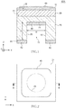
- FIG. 1 is a cross-sectional view illustrating the configuration of a Schottky barrier diode 10A according to the first embodiment of the present invention.
- FIG. 2 is a top view of the Schottky barrier diode 10A.
- the cross section illustrated in FIG. 1 corresponds to the cross section taken along line A-A in FIG. 2 .
- the Schottky barrier diode 10A includes a semiconductor substrate 20 and an epitaxial layer 30, both of which are made of gallium oxide ( ⁇ -Ga 2 O 3 ).
- the semiconductor substrate 20 and epitaxial layer 30 each contain, as an n-type dopant, silicon (Si) or tin (Sn).
- the concentration of the dopant is higher in the semiconductor substrate 20 than in the epitaxial layer 30 and, as a result, the semiconductor substrate 20 and the epitaxial layer 30 function as an n + layer and an n - layer, respectively.
- the semiconductor substrate 20 is obtained by cutting a bulk crystal formed using a melt-growing method, and the thickness (height in the Z-direction) thereof is preferably at least equal to or larger than 50 ⁇ m and more preferably about 250 ⁇ m. This is because when the thickness of the semiconductor substrate 20 is smaller than 50 ⁇ m, the mechanical strength becomes insufficient, and the element becomes difficult to handle at manufacturing or mounting. On the other hand, when the thickness of the semiconductor substrate 20 is about 250 ⁇ m, it is possible to ensure sufficient mechanical strength and handling performance.
- planar size of the semiconductor substrate 20 is generally selected in accordance with the amount of current flowing in the element and, when the maximum amount of forward current is about 20A, the widths in the X- and Y-directions may be set to about 2.4 mm.
- the semiconductor substrate 20 has a first surface 21 positioned on the upper surface side in a mounted state and a second surface 22 opposite to the first surface 21, positioned on the lower surface side in a mounted state.
- the epitaxial layer 30 is formed on the entire first surface 21.
- the epitaxial layer 30 is a thin film obtained by epitaxially growing gallium oxide on the first surface 21 of the semiconductor substrate 20 using a reactive sputtering method, a PLD method, an MBE method, an MOCVD method, or an HVPE method and functions as a drift layer.
- the film thickness of the epitaxial layer 30 is generally selected in accordance with the backward withstand voltage of the element and, in order to ensure a withstand voltage of about 600 V, the film thickness may be set to, e.g., about 7 ⁇ m.
- a recessed part 23 is formed in the second surface 22 of the semiconductor substrate 20 to selectively reduce the thickness of the semiconductor substrate 20 at this portion.
- the shape of the recessed part 23 as viewed in the Z-direction is a circular shape, but not limited thereto.
- the recessed part 23 can be formed by anisotropically etching the semiconductor substrate 20 from the second surface 22 side using, e.g., chlorine-based gas such as BCl 3 .
- a bottom surface 24 of the recessed part 23 constitutes the XY plane parallel to the first surface 21, and an inner wall surface 25 of the recessed part 23 constitutes a curved surface parallel to the Z-direction.
- the bottom surface 24 need not be completely parallel to the first surface 21 as long as it overlaps the first surface 21 in a plan view. Accordingly, the bottom surface 24 may be inclined or bent relative to the XY plane. Further, the inner wall surface 25 also need not be a vertical surface completely parallel to the Z-direction as long as it connects the bottom surface 24 and the second surface 22. Accordingly, the inner wall surface 25 may be inclined relative to the Z-direction.
- the depth D may be set to about 50 ⁇ m to about 225 ⁇ m, and the diameter W may be set to about 100 ⁇ m to about 200 ⁇ m.
- the depth D is preferably set such that the thickness of the semiconductor substrate 20 at the portion where the recessed part 23 is formed, i.e., the distance between the first surface 21 and the bottom surface 24 in the Z-direction is 50 ⁇ m or larger. This is because when the thickness of the semiconductor substrate 20 at this position is smaller than 50 ⁇ m, mechanical strength at this portion becomes insufficient, which may cause breakage of the semiconductor substrate 20 at wire bonding.
- the thickness of the semiconductor substrate 20 at the position where the recessed part 23 is formed is preferably set to 100 ⁇ m or smaller.
- an insulating film 31 having an opening 32 is formed on the upper surface of the epitaxial layer 30, and an anode electrode 40 is formed on the insulating film 31.
- the anode electrode 40 is brought into Schottky contact with the epitaxial layer 30 through the opening 32 of the insulating film 31.
- the insulating film 31 is made of, e.g., silicon oxide (SiO 2 ), and the film thickness thereof is about 300 nm.
- the anode electrode 40 is formed of a laminated film of, e.g., platinum (Pt), titanium (Ti), and gold (Au), and the film thickness thereof is about 150 nm (Pt layer), about 5 nm (Ti layer), and about 230 nm (Au layer).
- the anode electrode 40 is provided at a position that overlaps the recessed part 23 in a plan view (as viewed in the Z-direction which is the lamination direction).
- the XY area of the recessed part 23 is preferably smaller than the XY area of the anode electrode 40 so that the recessed part 23 completely overlaps the anode electrode 40 in a plan view.
- the XY area of the recessed part 23 is excessively small, a heat radiating effect to be described later becomes insufficient, so that the XY area of the recessed part 23 is preferably 50 % or more of the XY area of the anode electrode 40.
- a cathode electrode 50 is provided on the second surface 22 of the semiconductor substrate 20.
- the cathode electrode 50 is formed on the bottom surface 24 of the recessed part 23 and on the second surface 22 positioned outside the recessed part 23 and is brought into ohmic contact with the semiconductor substrate 20.
- the cathode electrode 50 need not necessarily be formed outside the recessed part 23; however, it is preferable to form the cathode electrode 50 also outside the recessed part 23 as illustrated in FIG. 1 in terms of connection reliability to a circuit substrate at mounting and solder wettability.
- the anode electrode 40 and the cathode electrode 50 face each other in the Z-direction through the epitaxial layer 30 and the semiconductor substrate 20 having the recessed part 23.
- forward voltage when forward voltage is applied between the anode electrode 40 and the cathode electrode 50, forward current flows in a portion thinned by the recessed part 23. That is, the length of a current path between the anode electrode 40 and the cathode electrode 50 is reduced as compared to a case where the recessed part 23 is not formed, allowing reduction in heat generation due to the resistance component of gallium oxide.
- the thickness of the semiconductor substrate 20 is reduced at only the recessed part 23, and a sufficient thickness is ensured outside the recessed part 23, making it possible to endure the mechanical strength of the semiconductor substrate 20 and the handling performance thereof.
- FIG. 3 is a cross-sectional view illustrating a part of an electronic circuit 100 provided with the Schottky barrier diode 10A according to the present embodiment.
- the electronic circuit 100 illustrated in FIG. 3 includes a circuit board 60 having an electrode pattern 61 and the Schottky barrier diode 10A mounted on the circuit board 60.
- the anode electrode 40 of the Schottky barrier diode 10A is connected to another electrode pattern (not shown) through a bonding wire 62, and the cathode electrode 50 of the Schottky barrier diode 10A is connected to the electrode pattern 61 through a solder 63.
- solder 63 As illustrated in FIG. 3 , a part of the solder 63 is embedded in the recessed part 23 formed in the semiconductor substrate 20. As a result, the cathode electrode 50 formed on the bottom surface 24 of the recessed part 23 and the electrode pattern 61 are electrically connected to each other through the solder 63.
- the solder 63 has a significantly higher heat conductivity than the semiconductor substrate 20 made of gallium oxide, so that heat generated when forward current is made to flow in the Schottky barrier diode 10A is efficiently radiated to the circuit board 60 side through the solder 63 embedded in the recessed part 23. Thus, even though gallium oxide having a low heat conductivity is used as the material of the semiconductor substrate 20, a high heat radiation performance can be ensured.
- the conductive member connecting the cathode electrode 50 and the electrode pattern 61 is not limited to the solder 63, and other conductive members may be used.
- the thickness of the semiconductor substrate 20 is selectively reduced at the portion where the recessed part 23 is formed, so that it is possible to suppress heat generation and achieve a satisfactory heat radiation performance while ensuring mechanical strength and handling performance.
- the Schottky barrier diode 10A can be suitably used as a switching device for a power device.
- FIG. 4 is a cross-sectional view illustrating the configuration of a Schottky barrier diode 10B according to the second embodiment of the present invention.
- the Schottky barrier diode 10B according to the second embodiment of the present invention differs from the Schottky barrier diode 10A according to the first embodiment in that the cathode electrode 50 is formed also on the inner wall surface 25 of the recessed part 23.
- Other configurations are the same as those of the Schottky barrier diode 10A according to the first embodiment, so the same reference numerals are given to the same elements, and overlapping description will be omitted.
- the cathode electrode 50 is formed also on the inner wall surface 25 of the recessed part 23, so that the area of ohmic contact between the semiconductor substrate 20 and the cathode electrode 50 can be increased.
- the wettability of the solder 63 embedded in the recessed part 23 is improved by the cathode electrode 50 formed on the inner wall surface 25 of the recessed part 23, thereby enhancing connection reliability.
- FIG. 5 is a top view illustrating the configuration of a Schottky barrier diode 10C according to the third embodiment of the present invention.
- the Schottky barrier diode 10C according to the third embodiment of the present invention differs from the Schottky barrier diode 10A according to the first embodiment in that communication holes 23a connecting the recessed part 23 and the side surface of the semiconductor substrate 20 are formed in the semiconductor substrate 20.
- Other configurations are the same as those of the Schottky barrier diode 10A according to the first embodiment, so the same reference numerals are given to the same elements, and overlapping description will be omitted.
- FIG. 6 is a cross-sectional view illustrating the configuration of a Schottky barrier diode 10D according to the fourth embodiment of the present invention.
- FIG. 7 is a bottom view of the semiconductor substrate 20 used in the present embodiment as viewed from the second surface 22 side.
- the Schottky barrier diode 10D according to the fourth embodiment of the present invention differs from the Schottky barrier diode 10A according to the first embodiment in that the recessed part 23 is constituted of a plurality of slits.
- Other configurations are the same as those of the Schottky barrier diode 10A according to the first embodiment, so the same reference numerals are given to the same elements, and overlapping description will be omitted.
- the recessed part 23 is constituted of six slits extending in the Y-direction.
- the mechanical strength of the semiconductor substrate 20 can be enhanced as compared to the first embodiment.
- FIG. 8 is a bottom view illustrating the configuration of a Schottky barrier diode 10E according to the fifth embodiment of the present invention.
- the Schottky barrier diode 10E according to the fifth embodiment of the present invention differs from the Schottky barrier diode 10A according to the first embodiment in that the recessed part 23 is formed in a mesh.
- Other configurations are the same as those of the Schottky barrier diode 10A according to the first embodiment, so the same reference numerals are given to the same elements, and overlapping description will be omitted.
- the recessed part 23 is constituted of six slits extending in the X-direction and six slits extending in the Y-direction, which cross each other to form the recessed part 23 into a mesh in a plan view.
- the mechanical strength of the semiconductor substrate 20 can be enhanced as compared to the first embodiment.
- the air layer is more difficult to form in the recessed part 23 than in the case of the fifth embodiment.
- a simulation model having the same configuration as the electronic circuit 100 illustrated in FIG. 3 was assumed, and Au was used as the materials of the anode electrode 40 and cathode electrode 50.
- an element temperature was simulated with the depth D and diameter W of the recessed part 23 variously changed.
- the planar shape of the recessed part 23 was a square.
- the dimensions of the semiconductor substrate 20 in the X-, Y-, and Z-directions were 2.4 mm, 2.4 mm, and 250 ⁇ m
- the dimensions of the anode electrode 40 in the X-, Y-, and Z-directions were 2.1 mm, 2.1 mm, and 0.3 ⁇ m.
- the solder 63 was fully filled in the entire recessed part 23 and had a thickness of 50 ⁇ m from the second surface 22 found outside the recessed part 23. Then, temperature at the center of the anode electrode 40 was simulated with an assumption that forward current was made to flow from the anode electrode 40 to the cathode electrode 50 so as to hold the temperature of a cold plate corresponding to the circuit board 60 at 25°C and to set consumption power to 2.4 W.
- the temperature rises up to 54.9°C when the recessed part 23 is not formed in the semiconductor substrate 20, while the temperature is suppressed to 50°C or lower when the recessed part 23 is formed in the semiconductor substrate 20.
- the depth D of the recessed part 23 is 200 ⁇ m or larger, the temperature is suppressed to about 40°C or lower, and thus a significantly high heat radiation effect can be obtained.
- the area of the recessed part 23 is about 23% of the area of the anode electrode 40 when the width W of the recessed part 23 is 1 mm, and the area of the recessed part 23 is about 91% of the area of the anode electrode 40 when the width W of the recessed part 23 is 2 mm.
Landscapes
- Electrodes Of Semiconductors (AREA)
Abstract
Description
- The present invention relates to a Schottky barrier diode and an electronic circuit provided with the same and, more particularly, to a Schottky barrier diode using gallium oxide and an electronic circuit provided with the same.
- A Schottky barrier diode is a rectifying element utilizing a Schottky barrier generated due to bonding between metal and a semiconductor and is lower in forward voltage and higher in switching speed than a normal diode having a PN junction. Thus, the Schottky barrier diode may be utilized as a switching element for a power device.
- When the Schottky barrier diode is utilized as a switching element for a power device, it is necessary to ensure a sufficient backward withstand voltage, so that, silicon carbide (SiC), gallium nitride (GaN), or gallium oxide (Ga2O3) having a larger band gap may be used in place of silicon (Si) . Among them, gallium oxide has a very large band gap (4.8 eV to 4.9 eV) and a large breakdown field (7 MV/cm to 8 MV/cm), so that a Schottky barrier diode using gallium oxide is very promising as the switching element for a power device. Patent Document 1 describes an example of the Schottky barrier diode using gallium oxide.
- However, gallium oxide has a significantly lower heat conductivity than silicon (Si), silicon carbide (SiC), and gallium nitride (GaN). Thus, when a Schottky barrier diode using gallium oxide is used as the switching element for a power device, heat generated by forward current is not efficiently radiated outside to easily deteriorate the element. To cope with this problem, in the Schottky barrier diode described in Patent Document 1, the thickness of a gallium oxide substrate is reduced to 50 µm or less to thereby enhance heat radiation performance while suppressing heat generation due to forward current.
- [Patent Document 1]
JP 2016-031953 A - However, simple reduction in the thickness of the gallium oxide substrate may not only cause shortage of mechanical strength of the element but also make the element difficult to handle at manufacturing or mounting.
- It is therefore an object of the present invention to provide a Schottky barrier diode using gallium oxide capable of suppressing heat generation and enhancing heat radiation performance while ensuring mechanical strength and handling performance.
- A Schottky barrier diode according to the present invention includes: a semiconductor substrate made of gallium oxide, having a first surface and a second surface positioned on the side opposite to the first surface, and having a recessed part on the second surface side; an epitaxial layer made of gallium oxide and provided on the first surface of the semiconductor substrate; an anode electrode provided at a position overlapping the recessed part as viewed in the lamination direction and brought into Schottky contact with the epitaxial layer; and a cathode electrode provided in the recessed part of the semiconductor substrate and brought into ohmic contact with the semiconductor substrate.
- Further, an electronic circuit according to the present invention includes: a circuit board having an electrode pattern; the Schottky barrier diode mounted on the circuit board; and a conductive member at least partially embedded in the recessed part of the semiconductor substrate and connecting the electrode pattern and the cathode electrode.
- According to the present invention, since the recessed part is provided in the semiconductor substrate made of gallium oxide, the thickness of the semiconductor substrate at a part thereof where forward current flows can be selectively reduced. This makes it possible to suppress heat generation and to enhance heat radiation performance while ensuring mechanical strength and handling performance. Thus, even though gallium oxide having a low heat conductivity is used as the material of the semiconductor substrate, a temperature rise of the element can be suppressed.
- In the present invention, the recessed part of the semiconductor substrate preferably includes a bottom surface overlapping the first surface in a plan view and an inner wall surface connecting the bottom surface and the second surface, and the cathode electrode is preferably formed at least on the bottom surface of the recessed part. This can minimize the length of a current path for the forward current, making it possible to further reduce heat generation.
- In this case, the cathode electrode may be formed further on the inner wall surface of the recessed part and further on the second surface positioned outside the recessed part. This improves solder wettability at mounting, enhancing mounting reliability.
- In the present invention, the area of recessed part as viewed in the lamination direction is preferably smaller than the area of the anode electrode. This makes it possible to minimize reduction in mechanical strength due to existence of the recessed part while suppressing heat generation due to forward current. Even in this case, the area of the recessed part as viewed in the lamination direction is preferably 50% or more of the area of the anode electrode. This can enhance heat radiation performance sufficiently.
- In the present invention, the thickness of the semiconductor substrate at the position where the recessed part is formed is preferably 50 µm or larger. Thus, a certain degree of mechanical strength can be ensured even at the formation position of the recessed part, making it difficult to cause breakage of the semiconductor substrate even when wire bonding is applied to the anode electrode.
- In the present invention, the recessed part preferably communicates with the side surface of the semiconductor substrate. With this configuration, air residing in the recessed part is discharged outside when a solder is embedded in the recessed part at mounting, thereby preventing an air layer from being formed in the recessed part. This prevents heat radiation performance from being impaired by the air layer. In this case, the recessed part may be constituted of a plurality of slits or formed in a mesh.
- As described above, according to the present invention, it is possible to suppress heat generation and to enhance heat radiation performance while ensuring mechanical strength and handling performance of the Schottky barrier diode using gallium oxide. Thus, even though gallium oxide having a low heat conductivity is used, a temperature rise of the element can be suppressed.
-
-
FIG. 1 is a cross-sectional view illustrating the configuration of a Schottkybarrier diode 10A according to a first embodiment of the present invention. -
FIG. 2 is a top view of the Schottkybarrier diode 10A. -
FIG. 3 is a cross-sectional view illustrating a part of anelectronic circuit 100 provided with theSchottky barrier diode 10A. -
FIG. 4 is a cross-sectional view illustrating the configuration of a Schottkybarrier diode 10B according to a second embodiment of the present invention. -
FIG. 5 is a top view illustrating the configuration of a Schottkybarrier diode 10C according to a third embodiment of the present invention. -
FIG. 6 is a cross-sectional view illustrating the configuration of a Schottkybarrier diode 10D according to a fourth embodiment of the present invention. -
FIG. 7 is a bottom view of the Schottkybarrier diode 10D. -
FIG. 8 is a bottom view illustrating the configuration of a Schottkybarrier diode 10E according to a fifth embodiment of the present invention. - Preferred embodiments of the present invention will now be explained in detail with reference to the drawings.
-
FIG. 1 is a cross-sectional view illustrating the configuration of a Schottkybarrier diode 10A according to the first embodiment of the present invention.FIG. 2 is a top view of the Schottkybarrier diode 10A. The cross section illustrated inFIG. 1 corresponds to the cross section taken along line A-A inFIG. 2 . - As illustrated in
FIG. 1 , theSchottky barrier diode 10A according to the first embodiment includes asemiconductor substrate 20 and anepitaxial layer 30, both of which are made of gallium oxide (β-Ga2O3). Thesemiconductor substrate 20 andepitaxial layer 30 each contain, as an n-type dopant, silicon (Si) or tin (Sn). The concentration of the dopant is higher in thesemiconductor substrate 20 than in theepitaxial layer 30 and, as a result, thesemiconductor substrate 20 and theepitaxial layer 30 function as an n+ layer and an n- layer, respectively. - The
semiconductor substrate 20 is obtained by cutting a bulk crystal formed using a melt-growing method, and the thickness (height in the Z-direction) thereof is preferably at least equal to or larger than 50 µm and more preferably about 250 µm. This is because when the thickness of thesemiconductor substrate 20 is smaller than 50 µm, the mechanical strength becomes insufficient, and the element becomes difficult to handle at manufacturing or mounting. On the other hand, when the thickness of thesemiconductor substrate 20 is about 250 µm, it is possible to ensure sufficient mechanical strength and handling performance. While there is no particular restriction on the planar size of thesemiconductor substrate 20, the planar size is generally selected in accordance with the amount of current flowing in the element and, when the maximum amount of forward current is about 20A, the widths in the X- and Y-directions may be set to about 2.4 mm. - The
semiconductor substrate 20 has afirst surface 21 positioned on the upper surface side in a mounted state and asecond surface 22 opposite to thefirst surface 21, positioned on the lower surface side in a mounted state. Theepitaxial layer 30 is formed on the entirefirst surface 21. Theepitaxial layer 30 is a thin film obtained by epitaxially growing gallium oxide on thefirst surface 21 of thesemiconductor substrate 20 using a reactive sputtering method, a PLD method, an MBE method, an MOCVD method, or an HVPE method and functions as a drift layer. While there is no particular restriction on the film thickness of theepitaxial layer 30, the film thickness is generally selected in accordance with the backward withstand voltage of the element and, in order to ensure a withstand voltage of about 600 V, the film thickness may be set to, e.g., about 7 µm. - As illustrated in
FIGs. 1 and 2 , a recessedpart 23 is formed in thesecond surface 22 of thesemiconductor substrate 20 to selectively reduce the thickness of thesemiconductor substrate 20 at this portion. In the present embodiment, the shape of the recessedpart 23 as viewed in the Z-direction is a circular shape, but not limited thereto. The recessedpart 23 can be formed by anisotropically etching thesemiconductor substrate 20 from thesecond surface 22 side using, e.g., chlorine-based gas such as BCl3. In the example ofFIG. 1 , abottom surface 24 of the recessedpart 23 constitutes the XY plane parallel to thefirst surface 21, and aninner wall surface 25 of the recessedpart 23 constitutes a curved surface parallel to the Z-direction. However, thebottom surface 24 need not be completely parallel to thefirst surface 21 as long as it overlaps thefirst surface 21 in a plan view. Accordingly, thebottom surface 24 may be inclined or bent relative to the XY plane. Further, theinner wall surface 25 also need not be a vertical surface completely parallel to the Z-direction as long as it connects thebottom surface 24 and thesecond surface 22. Accordingly, theinner wall surface 25 may be inclined relative to the Z-direction. - While there is no particular restriction on a depth D and a diameter W of the recessed
part 23, when the thickness of thesemiconductor substrate 20 is 250 µm, the depth D may be set to about 50 µm to about 225 µm, and the diameter W may be set to about 100 µm to about 200 µm. Further, the depth D is preferably set such that the thickness of thesemiconductor substrate 20 at the portion where the recessedpart 23 is formed, i.e., the distance between thefirst surface 21 and thebottom surface 24 in the Z-direction is 50 µm or larger. This is because when the thickness of thesemiconductor substrate 20 at this position is smaller than 50 µm, mechanical strength at this portion becomes insufficient, which may cause breakage of thesemiconductor substrate 20 at wire bonding. On the other hand, when the depth D of the recessedpart 23 is excessively small, a sufficient heat generation suppressing effect or heat radiating effect cannot be obtained. Thus, the thickness of thesemiconductor substrate 20 at the position where the recessedpart 23 is formed is preferably set to 100 µm or smaller. - As illustrated in
FIG. 1 , an insulatingfilm 31 having anopening 32 is formed on the upper surface of theepitaxial layer 30, and ananode electrode 40 is formed on the insulatingfilm 31. As a result, theanode electrode 40 is brought into Schottky contact with theepitaxial layer 30 through theopening 32 of the insulatingfilm 31. The insulatingfilm 31 is made of, e.g., silicon oxide (SiO2), and the film thickness thereof is about 300 nm. Theanode electrode 40 is formed of a laminated film of, e.g., platinum (Pt), titanium (Ti), and gold (Au), and the film thickness thereof is about 150 nm (Pt layer), about 5 nm (Ti layer), and about 230 nm (Au layer). - As illustrated in
FIGs. 1 and 2 , theanode electrode 40 is provided at a position that overlaps the recessedpart 23 in a plan view (as viewed in the Z-direction which is the lamination direction). Particularly, the XY area of the recessedpart 23 is preferably smaller than the XY area of theanode electrode 40 so that the recessedpart 23 completely overlaps theanode electrode 40 in a plan view. However, when the XY area of the recessedpart 23 is excessively small, a heat radiating effect to be described later becomes insufficient, so that the XY area of the recessedpart 23 is preferably 50 % or more of the XY area of theanode electrode 40. - A
cathode electrode 50 is provided on thesecond surface 22 of thesemiconductor substrate 20. In the present embodiment, thecathode electrode 50 is formed on thebottom surface 24 of the recessedpart 23 and on thesecond surface 22 positioned outside the recessedpart 23 and is brought into ohmic contact with thesemiconductor substrate 20. In the present invention, thecathode electrode 50 need not necessarily be formed outside the recessedpart 23; however, it is preferable to form thecathode electrode 50 also outside the recessedpart 23 as illustrated inFIG. 1 in terms of connection reliability to a circuit substrate at mounting and solder wettability. - With the above configuration, the
anode electrode 40 and thecathode electrode 50 face each other in the Z-direction through theepitaxial layer 30 and thesemiconductor substrate 20 having the recessedpart 23. Thus, when forward voltage is applied between theanode electrode 40 and thecathode electrode 50, forward current flows in a portion thinned by the recessedpart 23. That is, the length of a current path between theanode electrode 40 and thecathode electrode 50 is reduced as compared to a case where the recessedpart 23 is not formed, allowing reduction in heat generation due to the resistance component of gallium oxide. In addition, the thickness of thesemiconductor substrate 20 is reduced at only the recessedpart 23, and a sufficient thickness is ensured outside the recessedpart 23, making it possible to endure the mechanical strength of thesemiconductor substrate 20 and the handling performance thereof. -
FIG. 3 is a cross-sectional view illustrating a part of anelectronic circuit 100 provided with theSchottky barrier diode 10A according to the present embodiment. - The
electronic circuit 100 illustrated inFIG. 3 includes acircuit board 60 having anelectrode pattern 61 and theSchottky barrier diode 10A mounted on thecircuit board 60. Theanode electrode 40 of theSchottky barrier diode 10A is connected to another electrode pattern (not shown) through abonding wire 62, and thecathode electrode 50 of theSchottky barrier diode 10A is connected to theelectrode pattern 61 through asolder 63. - As illustrated in
FIG. 3 , a part of thesolder 63 is embedded in the recessedpart 23 formed in thesemiconductor substrate 20. As a result, thecathode electrode 50 formed on thebottom surface 24 of the recessedpart 23 and theelectrode pattern 61 are electrically connected to each other through thesolder 63. Thesolder 63 has a significantly higher heat conductivity than thesemiconductor substrate 20 made of gallium oxide, so that heat generated when forward current is made to flow in theSchottky barrier diode 10A is efficiently radiated to thecircuit board 60 side through thesolder 63 embedded in the recessedpart 23. Thus, even though gallium oxide having a low heat conductivity is used as the material of thesemiconductor substrate 20, a high heat radiation performance can be ensured. The conductive member connecting thecathode electrode 50 and theelectrode pattern 61 is not limited to thesolder 63, and other conductive members may be used. - As described above, in the
Schottky barrier diode 10A according to the present embodiment, the thickness of thesemiconductor substrate 20 is selectively reduced at the portion where the recessedpart 23 is formed, so that it is possible to suppress heat generation and achieve a satisfactory heat radiation performance while ensuring mechanical strength and handling performance. Thus, theSchottky barrier diode 10A can be suitably used as a switching device for a power device. - Hereinafter, other embodiments of the present invention will be described.
-
FIG. 4 is a cross-sectional view illustrating the configuration of aSchottky barrier diode 10B according to the second embodiment of the present invention. - As illustrated in
FIG. 4 , theSchottky barrier diode 10B according to the second embodiment of the present invention differs from theSchottky barrier diode 10A according to the first embodiment in that thecathode electrode 50 is formed also on theinner wall surface 25 of the recessedpart 23. Other configurations are the same as those of theSchottky barrier diode 10A according to the first embodiment, so the same reference numerals are given to the same elements, and overlapping description will be omitted. - In the present embodiment, the
cathode electrode 50 is formed also on theinner wall surface 25 of the recessedpart 23, so that the area of ohmic contact between thesemiconductor substrate 20 and thecathode electrode 50 can be increased. In addition, the wettability of thesolder 63 embedded in the recessedpart 23 is improved by thecathode electrode 50 formed on theinner wall surface 25 of the recessedpart 23, thereby enhancing connection reliability. -
FIG. 5 is a top view illustrating the configuration of aSchottky barrier diode 10C according to the third embodiment of the present invention. - As illustrated in
FIG. 5 , theSchottky barrier diode 10C according to the third embodiment of the present invention differs from theSchottky barrier diode 10A according to the first embodiment in thatcommunication holes 23a connecting the recessedpart 23 and the side surface of thesemiconductor substrate 20 are formed in thesemiconductor substrate 20. Other configurations are the same as those of theSchottky barrier diode 10A according to the first embodiment, so the same reference numerals are given to the same elements, and overlapping description will be omitted. - In the example of
FIG. 5 , fourcommunication holes 23a are formed, making the recessedpart 23 communicate with the XZ and YZ side surfaces . Thus, when thesolder 63 is embedded in the recessedpart 23 at mounting on thecircuit board 60, air residing in the recessedpart 23 is discharged outside through thecommunication holes 23a. This prevents an air layer from being formed in the recessedpart 23, thereby preventing heat radiation performance from being impaired by the air layer. -
FIG. 6 is a cross-sectional view illustrating the configuration of aSchottky barrier diode 10D according to the fourth embodiment of the present invention.FIG. 7 is a bottom view of thesemiconductor substrate 20 used in the present embodiment as viewed from thesecond surface 22 side. - As illustrated in
FIGs. 6 and 7 , theSchottky barrier diode 10D according to the fourth embodiment of the present invention differs from theSchottky barrier diode 10A according to the first embodiment in that the recessedpart 23 is constituted of a plurality of slits. Other configurations are the same as those of theSchottky barrier diode 10A according to the first embodiment, so the same reference numerals are given to the same elements, and overlapping description will be omitted. - In the present embodiment, the recessed
part 23 is constituted of six slits extending in the Y-direction. By making the recessedpart 23 into such a shape, the mechanical strength of thesemiconductor substrate 20 can be enhanced as compared to the first embodiment. Further, like the third embodiment, it is possible to prevent an air layer from being formed in the recessedpart 23 at mounting on thecircuit board 60 using thesolder 63. -
FIG. 8 is a bottom view illustrating the configuration of aSchottky barrier diode 10E according to the fifth embodiment of the present invention. - As illustrated in
FIG. 8 , theSchottky barrier diode 10E according to the fifth embodiment of the present invention differs from theSchottky barrier diode 10A according to the first embodiment in that the recessedpart 23 is formed in a mesh. Other configurations are the same as those of theSchottky barrier diode 10A according to the first embodiment, so the same reference numerals are given to the same elements, and overlapping description will be omitted. - In the present embodiment, the recessed
part 23 is constituted of six slits extending in the X-direction and six slits extending in the Y-direction, which cross each other to form the recessedpart 23 into a mesh in a plan view. By forming the recessedpart 23 into such a shape, the mechanical strength of thesemiconductor substrate 20 can be enhanced as compared to the first embodiment. Further, the air layer is more difficult to form in the recessedpart 23 than in the case of the fifth embodiment. - It is apparent that the present invention is not limited to the above embodiments, but may be modified and changed without departing from the scope and spirit of the invention.
- A simulation model having the same configuration as the
electronic circuit 100 illustrated inFIG. 3 was assumed, and Au was used as the materials of theanode electrode 40 andcathode electrode 50. Using this simulation model, an element temperature was simulated with the depth D and diameter W of the recessedpart 23 variously changed. The planar shape of the recessedpart 23 was a square. In the simulation model, the dimensions of thesemiconductor substrate 20 in the X-, Y-, and Z-directions were 2.4 mm, 2.4 mm, and 250 µm, and the dimensions of theanode electrode 40 in the X-, Y-, and Z-directions were 2.1 mm, 2.1 mm, and 0.3 µm. Thesolder 63 was fully filled in the entire recessedpart 23 and had a thickness of 50 µm from thesecond surface 22 found outside the recessedpart 23. Then, temperature at the center of theanode electrode 40 was simulated with an assumption that forward current was made to flow from theanode electrode 40 to thecathode electrode 50 so as to hold the temperature of a cold plate corresponding to thecircuit board 60 at 25°C and to set consumption power to 2.4 W. - The simulation results are shown in Table 1.
[Table 1] D (µm) 0 100 200 225 100 150 200 225 W (mm) 0 1 1 1 2 2 2 2 Temperature (°C) 54.9 48.6 40.1 39.6 48.5 43.9 39.7 39.1 - As shown in Table 1, the temperature rises up to 54.9°C when the recessed
part 23 is not formed in thesemiconductor substrate 20, while the temperature is suppressed to 50°C or lower when the recessedpart 23 is formed in thesemiconductor substrate 20. In particular, when the depth D of the recessedpart 23 is 200 µm or larger, the temperature is suppressed to about 40°C or lower, and thus a significantly high heat radiation effect can be obtained. - Further, the larger the depth D of the recessed
part 23 is, the lower the element temperature becomes; however, there is no significant difference between when the depth D is 200 µm and when it is 225 µm. When the depth D is 225 µm, the thickness of thesemiconductor substrate 20 is reduced to 25 µm, which may cause shortage of mechanical strength. Considering this, depth D = 200 µm is advantageous over depth D = 225 µm. - The area of the recessed
part 23 is about 23% of the area of theanode electrode 40 when the width W of the recessedpart 23 is 1 mm, and the area of the recessedpart 23 is about 91% of the area of theanode electrode 40 when the width W of the recessedpart 23 is 2 mm. Although no significant difference is found between the case when the width W is 1 mm and the case when it is 2 mm, it is recognized that the element temperature becomes lower as the width W of the recessedpart 23 is larger. -
- 10A-10E
- Schottky barrier diode
- 20
- semiconductor substrate
- 21
- first surface
- 22
- second surface
- 23
- recessed part
- 23a
- communication hole
- 24
- bottom surface
- 25
- inner wall surface
- 30
- epitaxial layer
- 31
- insulating film
- 32
- opening
- 40
- anode electrode
- 50
- cathode electrode
- 60
- circuit board
- 61
- electrode pattern
- 62
- bonding wire
- 63
- solder
- 100
- electronic circuit
Claims (11)
- A Schottky barrier diode comprising:a semiconductor substrate made of gallium oxide, the semiconductor substrate having a first surface, a second surface opposite to the first surface, and a recessed part formed on the second surface;an epitaxial layer made of gallium oxide, the epitaxial layer being provided on the first surface of the semiconductor substrate;an anode electrode provided at a position overlapping the recessed part as viewed in a lamination direction and brought into Schottky contact with the epitaxial layer; anda cathode electrode provided in the recessed part of the semiconductor substrate and brought into ohmic contact with the semiconductor substrate.
- The Schottky barrier diode as claimed in claim 1,
wherein the recessed part of the semiconductor substrate includes a bottom surface overlapping the first surface in a plan view and an inner wall surface connecting the bottom surface and the second surface, and
wherein the cathode electrode is formed at least on the bottom surface of the recessed part. - The Schottky barrier diode as claimed in claim 2, wherein the cathode electrode is formed further on the inner wall surface of the recessed part.
- The Schottky barrier diode as claimed in claim 2 or 3, wherein the cathode electrode is formed further on the second surface positioned outside the recessed part.
- The Schottky barrier diode as claimed in any one of claims 2 to 4, wherein an area of recessed part as viewed in the lamination direction is smaller than an area of the anode electrode.
- The Schottky barrier diode as claimed in claim 5, wherein the area of the recessed part as viewed in the lamination direction is 50% or more of the area of the anode electrode.
- The Schottky barrier diode as claimed in any one of claims 1 to 6, wherein a thickness of the semiconductor substrate at a position where the recessed part is formed is 50 µm or larger.
- The Schottky barrier diode as claimed in any one of claims 1 to 7, wherein the recessed part communicates with a side surface of the semiconductor substrate.
- The Schottky barrier diode as claimed in claim 8, wherein the recessed part is constituted of a plurality of slits.
- The Schottky barrier diode as claimed in claim 8, wherein the recessed part is formed in a mesh.
- An electronic circuit comprising:a circuit board having an electrode pattern;the Schottky barrier diode as claimed in any one of claims 1 to 10 mounted on the circuit board; anda conductive member at least partially embedded in the recessed part of the semiconductor substrate and connecting the electrode pattern and the cathode electrode.
Applications Claiming Priority (2)
| Application Number | Priority Date | Filing Date | Title |
|---|---|---|---|
| JP2016218652A JP6812758B2 (en) | 2016-11-09 | 2016-11-09 | Schottky barrier diode and electronic circuit equipped with it |
| PCT/JP2017/032612 WO2018088018A1 (en) | 2016-11-09 | 2017-09-11 | Schottky barrier diode and electronic circuit provided with same |
Publications (3)
| Publication Number | Publication Date |
|---|---|
| EP3540784A1 true EP3540784A1 (en) | 2019-09-18 |
| EP3540784A4 EP3540784A4 (en) | 2020-05-20 |
| EP3540784B1 EP3540784B1 (en) | 2023-08-16 |
Family
ID=62110519
Family Applications (1)
| Application Number | Title | Priority Date | Filing Date |
|---|---|---|---|
| EP17869159.8A Active EP3540784B1 (en) | 2016-11-09 | 2017-09-11 | Schottky barrier diode and electronic circuit provided with same |
Country Status (5)
| Country | Link |
|---|---|
| US (1) | US10840384B2 (en) |
| EP (1) | EP3540784B1 (en) |
| JP (1) | JP6812758B2 (en) |
| CN (1) | CN109923678B (en) |
| WO (1) | WO2018088018A1 (en) |
Cited By (4)
| Publication number | Priority date | Publication date | Assignee | Title |
|---|---|---|---|---|
| TWI812149B (en) * | 2021-04-15 | 2023-08-11 | 中國商蘇州晶湛半導體有限公司 | Semiconductor structure and its preparation method |
| EP4084043A4 (en) * | 2019-12-26 | 2024-01-03 | Tamura Corporation | SEMICONDUCTOR ELEMENT, METHOD FOR PRODUCING A SEMICONDUCTOR ELEMENT, SEMICONDUCTOR COMPONENT AND METHOD FOR PRODUCING A SEMICONDUCTOR COMPONENT |
| EP4084064A4 (en) * | 2019-12-26 | 2024-01-24 | Tamura Corporation | Semiconductor device |
| US12635520B2 (en) | 2019-12-26 | 2026-05-19 | Tamura Corporation | Semiconductor element, method for manufacturing semiconductor element, semiconductor device, and method for manufacturing semiconductor device |
Families Citing this family (15)
| Publication number | Priority date | Publication date | Assignee | Title |
|---|---|---|---|---|
| CN110809826B (en) * | 2017-06-29 | 2022-10-28 | 三菱电机株式会社 | Oxide semiconductor device and method for manufacturing oxide semiconductor device |
| JP2020043126A (en) * | 2018-09-06 | 2020-03-19 | 住友電気工業株式会社 | Silicon carbide semiconductor device and silicon carbide semiconductor module |
| CN109920857B (en) * | 2019-03-19 | 2021-11-30 | 珠海镓未来科技有限公司 | Schottky diode and preparation method thereof |
| JP7316865B2 (en) | 2019-07-22 | 2023-07-28 | ルネサスエレクトロニクス株式会社 | semiconductor equipment |
| CN112382665A (en) * | 2020-11-03 | 2021-02-19 | 广东省科学院半导体研究所 | Gallium oxide-based MOSFET device and manufacturing method thereof |
| CN112382664A (en) * | 2020-11-03 | 2021-02-19 | 广东省科学院半导体研究所 | Flip MOSFET device and manufacturing method thereof |
| CN116169157A (en) * | 2021-11-25 | 2023-05-26 | 广州华瑞升阳投资有限公司 | A gallium oxide device and its preparation method |
| CN114446904A (en) * | 2021-12-30 | 2022-05-06 | 光梓信息科技(深圳)有限公司 | Wafer packaging structure and method based on nanoscale radiator |
| WO2023181801A1 (en) * | 2022-03-24 | 2023-09-28 | ローム株式会社 | Semiconductor device and method for manufacturing same |
| CN115911134A (en) * | 2022-10-12 | 2023-04-04 | 西安电子科技大学 | Gallium oxide field termination power diode and preparation method thereof |
| CN116207164A (en) * | 2023-03-26 | 2023-06-02 | 湖北九峰山实验室 | Multistage groove self-protection Schottky diode device and manufacturing method |
| CN118173547B (en) * | 2024-04-10 | 2024-11-05 | 安徽长飞先进半导体股份有限公司 | Power device, power module, power conversion circuit and vehicle |
| CN118352402B (en) * | 2024-04-17 | 2026-02-10 | 中国科学院半导体研究所 | Gallium oxide devices and their fabrication methods |
| CN119630005B (en) * | 2024-11-08 | 2025-10-17 | 西安电子科技大学 | Low-cost thermally enhanced gallium nitride Schottky barrier diode and preparation method thereof |
| CN119317204A (en) * | 2024-12-05 | 2025-01-14 | 浙江大学 | A semiconductor optoelectronic device |
Family Cites Families (18)
| Publication number | Priority date | Publication date | Assignee | Title |
|---|---|---|---|---|
| JP2868194B2 (en) | 1992-03-25 | 1999-03-10 | 松下電工株式会社 | Heat dissipation structure in semiconductor device |
| JPH07336009A (en) | 1994-06-10 | 1995-12-22 | Fujitsu General Ltd | Heat dissipation structure of semiconductor element |
| JP4744682B2 (en) * | 2000-09-21 | 2011-08-10 | 三菱電機株式会社 | Schottky barrier diode |
| JP2002170963A (en) * | 2000-12-01 | 2002-06-14 | Sanken Electric Co Ltd | Semiconductor element, semiconductor device, and method of manufacturing semiconductor element |
| JP2006156658A (en) * | 2004-11-29 | 2006-06-15 | Toshiba Corp | Semiconductor device |
| JP4907955B2 (en) * | 2005-11-10 | 2012-04-04 | パナソニック株式会社 | Schottky barrier diode and manufacturing method thereof |
| CN101499480B (en) | 2008-01-30 | 2013-03-20 | 松下电器产业株式会社 | Semiconductor chip and semiconductor device |
| JP2009182217A (en) * | 2008-01-31 | 2009-08-13 | Sumitomo Electric Ind Ltd | Semiconductor device and manufacturing method thereof |
| JP2010182958A (en) * | 2009-02-06 | 2010-08-19 | Seiko Instruments Inc | Semiconductor device and method of manufacturing semiconductor device |
| US7842974B2 (en) * | 2009-02-18 | 2010-11-30 | Alpha & Omega Semiconductor, Inc. | Gallium nitride heterojunction schottky diode |
| WO2013035472A1 (en) * | 2011-09-08 | 2013-03-14 | 株式会社タムラ製作所 | Substrate for epitaxial growth, and crystal laminate structure |
| JP2013102081A (en) | 2011-11-09 | 2013-05-23 | Tamura Seisakusho Co Ltd | Schottky barrier diode |
| JP5841417B2 (en) * | 2011-11-30 | 2016-01-13 | 株式会社日立製作所 | Nitride semiconductor diode |
| JP6065198B2 (en) * | 2012-02-21 | 2017-01-25 | ローム株式会社 | Semiconductor device and manufacturing method of semiconductor device |
| JP6004561B2 (en) * | 2012-03-30 | 2016-10-12 | 国立研究開発法人産業技術総合研究所 | Method for manufacturing silicon carbide semiconductor element |
| JP6137955B2 (en) * | 2013-06-14 | 2017-05-31 | 新電元工業株式会社 | Silicon carbide semiconductor device and method for manufacturing silicon carbide semiconductor device |
| JP2016031953A (en) | 2014-07-25 | 2016-03-07 | 株式会社タムラ製作所 | Semiconductor device and method for manufacturing the same, semiconductor substrate, and crystal laminate structure |
| CN112038416B (en) * | 2020-09-15 | 2021-09-03 | 西安电子科技大学 | Schottky diode based on p-type NiO film and inclined plane terminal structure and manufacturing method thereof |
-
2016
- 2016-11-09 JP JP2016218652A patent/JP6812758B2/en active Active
-
2017
- 2017-09-11 WO PCT/JP2017/032612 patent/WO2018088018A1/en not_active Ceased
- 2017-09-11 CN CN201780068998.0A patent/CN109923678B/en active Active
- 2017-09-11 US US16/348,592 patent/US10840384B2/en active Active
- 2017-09-11 EP EP17869159.8A patent/EP3540784B1/en active Active
Cited By (6)
| Publication number | Priority date | Publication date | Assignee | Title |
|---|---|---|---|---|
| EP4084043A4 (en) * | 2019-12-26 | 2024-01-03 | Tamura Corporation | SEMICONDUCTOR ELEMENT, METHOD FOR PRODUCING A SEMICONDUCTOR ELEMENT, SEMICONDUCTOR COMPONENT AND METHOD FOR PRODUCING A SEMICONDUCTOR COMPONENT |
| EP4084064A4 (en) * | 2019-12-26 | 2024-01-24 | Tamura Corporation | Semiconductor device |
| US12482729B2 (en) | 2019-12-26 | 2025-11-25 | Tamura Corporation | Semiconductor device |
| US12635520B2 (en) | 2019-12-26 | 2026-05-19 | Tamura Corporation | Semiconductor element, method for manufacturing semiconductor element, semiconductor device, and method for manufacturing semiconductor device |
| TWI812149B (en) * | 2021-04-15 | 2023-08-11 | 中國商蘇州晶湛半導體有限公司 | Semiconductor structure and its preparation method |
| US12419066B2 (en) | 2021-04-15 | 2025-09-16 | Enkris Semiconductor, Inc. | Semiconductor structures and manufacturing methods thereof |
Also Published As
| Publication number | Publication date |
|---|---|
| JP6812758B2 (en) | 2021-01-13 |
| EP3540784B1 (en) | 2023-08-16 |
| CN109923678A (en) | 2019-06-21 |
| US20200058804A1 (en) | 2020-02-20 |
| CN109923678B (en) | 2023-01-31 |
| US10840384B2 (en) | 2020-11-17 |
| EP3540784A4 (en) | 2020-05-20 |
| WO2018088018A1 (en) | 2018-05-17 |
| JP2018078177A (en) | 2018-05-17 |
Similar Documents
| Publication | Publication Date | Title |
|---|---|---|
| EP3540784B1 (en) | Schottky barrier diode and electronic circuit provided with same | |
| US11069783B2 (en) | Semiconductor device, semiconductor module, and packaged semiconductor device | |
| US9640632B2 (en) | Semiconductor device having improved heat dissipation | |
| CN102484124B (en) | Nitride semiconductor device | |
| EP1564815B1 (en) | Lateral conduction schottky diode with plural mesas | |
| US9324645B2 (en) | Method and system for co-packaging vertical gallium nitride power devices | |
| US8124983B2 (en) | Power transistor | |
| EP4084064B1 (en) | Semiconductor device | |
| US8937317B2 (en) | Method and system for co-packaging gallium nitride electronics | |
| TW202201804A (en) | Schottky barrier diode | |
| JP6795032B2 (en) | Semiconductor device | |
| CN104659025A (en) | Method and system for interleaved boost converter with co-packaged gallium nitride power devices | |
| US8884332B2 (en) | Nitride semiconductor device | |
| US10068780B2 (en) | Lead frame connected with heterojunction semiconductor body | |
| US12165957B2 (en) | Semiconductor device | |
| US12132122B2 (en) | Single chip power diode and method of producing a single chip power diode | |
| US20250357454A1 (en) | Power Semiconductor Device Stack, Power Module, and Method of Producing a Power Semiconductor Device Stack | |
| KR20260036942A (en) | Semiconductor device | |
| JP2026064941A (en) | Semiconductor equipment | |
| KR20250094031A (en) | Semiconductor device | |
| CN121057255A (en) | Semiconductor devices and their fabrication methods, electronic devices | |
| CN118571916A (en) | A P-channel device and integrated circuit thereof | |
| CN121057256A (en) | Semiconductor devices and their fabrication methods, electronic devices | |
| CN115868030A (en) | Barrier layer for electrical contact areas |
Legal Events
| Date | Code | Title | Description |
|---|---|---|---|
| STAA | Information on the status of an ep patent application or granted ep patent |
Free format text: STATUS: THE INTERNATIONAL PUBLICATION HAS BEEN MADE |
|
| PUAI | Public reference made under article 153(3) epc to a published international application that has entered the european phase |
Free format text: ORIGINAL CODE: 0009012 |
|
| STAA | Information on the status of an ep patent application or granted ep patent |
Free format text: STATUS: REQUEST FOR EXAMINATION WAS MADE |
|
| 17P | Request for examination filed |
Effective date: 20190606 |
|
| AK | Designated contracting states |
Kind code of ref document: A1 Designated state(s): AL AT BE BG CH CY CZ DE DK EE ES FI FR GB GR HR HU IE IS IT LI LT LU LV MC MK MT NL NO PL PT RO RS SE SI SK SM TR |
|
| AX | Request for extension of the european patent |
Extension state: BA ME |
|
| DAV | Request for validation of the european patent (deleted) | ||
| DAX | Request for extension of the european patent (deleted) | ||
| A4 | Supplementary search report drawn up and despatched |
Effective date: 20200421 |
|
| RIC1 | Information provided on ipc code assigned before grant |
Ipc: H01L 29/47 20060101ALI20200415BHEP Ipc: H01L 29/41 20060101ALI20200415BHEP Ipc: H01L 29/872 20060101AFI20200415BHEP Ipc: H01L 29/417 20060101ALI20200415BHEP Ipc: H01L 29/24 20060101ALI20200415BHEP Ipc: H01L 21/28 20060101ALI20200415BHEP Ipc: H01L 29/06 20060101ALI20200415BHEP |
|
| STAA | Information on the status of an ep patent application or granted ep patent |
Free format text: STATUS: EXAMINATION IS IN PROGRESS |
|
| 17Q | First examination report despatched |
Effective date: 20210414 |
|
| GRAP | Despatch of communication of intention to grant a patent |
Free format text: ORIGINAL CODE: EPIDOSNIGR1 |
|
| STAA | Information on the status of an ep patent application or granted ep patent |
Free format text: STATUS: GRANT OF PATENT IS INTENDED |
|
| INTG | Intention to grant announced |
Effective date: 20230216 |
|
| GRAJ | Information related to disapproval of communication of intention to grant by the applicant or resumption of examination proceedings by the epo deleted |
Free format text: ORIGINAL CODE: EPIDOSDIGR1 |
|
| STAA | Information on the status of an ep patent application or granted ep patent |
Free format text: STATUS: EXAMINATION IS IN PROGRESS |
|
| GRAS | Grant fee paid |
Free format text: ORIGINAL CODE: EPIDOSNIGR3 |
|
| STAA | Information on the status of an ep patent application or granted ep patent |
Free format text: STATUS: GRANT OF PATENT IS INTENDED |
|
| GRAP | Despatch of communication of intention to grant a patent |
Free format text: ORIGINAL CODE: EPIDOSNIGR1 |
|
| INTC | Intention to grant announced (deleted) | ||
| INTG | Intention to grant announced |
Effective date: 20230510 |
|
| GRAA | (expected) grant |
Free format text: ORIGINAL CODE: 0009210 |
|
| STAA | Information on the status of an ep patent application or granted ep patent |
Free format text: STATUS: THE PATENT HAS BEEN GRANTED |
|
| AK | Designated contracting states |
Kind code of ref document: B1 Designated state(s): AL AT BE BG CH CY CZ DE DK EE ES FI FR GB GR HR HU IE IS IT LI LT LU LV MC MK MT NL NO PL PT RO RS SE SI SK SM TR |
|
| REG | Reference to a national code |
Ref country code: GB Ref legal event code: FG4D |
|
| REG | Reference to a national code |
Ref country code: CH Ref legal event code: EP Ref country code: DE Ref legal event code: R096 Ref document number: 602017072916 Country of ref document: DE |
|
| REG | Reference to a national code |
Ref country code: IE Ref legal event code: FG4D |
|
| REG | Reference to a national code |
Ref country code: LT Ref legal event code: MG9D |
|
| REG | Reference to a national code |
Ref country code: NL Ref legal event code: MP Effective date: 20230816 |
|
| REG | Reference to a national code |
Ref country code: AT Ref legal event code: MK05 Ref document number: 1600949 Country of ref document: AT Kind code of ref document: T Effective date: 20230816 |
|
| PG25 | Lapsed in a contracting state [announced via postgrant information from national office to epo] |
Ref country code: GR Free format text: LAPSE BECAUSE OF FAILURE TO SUBMIT A TRANSLATION OF THE DESCRIPTION OR TO PAY THE FEE WITHIN THE PRESCRIBED TIME-LIMIT Effective date: 20231117 |
|
| PG25 | Lapsed in a contracting state [announced via postgrant information from national office to epo] |
Ref country code: IS Free format text: LAPSE BECAUSE OF FAILURE TO SUBMIT A TRANSLATION OF THE DESCRIPTION OR TO PAY THE FEE WITHIN THE PRESCRIBED TIME-LIMIT Effective date: 20231216 |
|
| PG25 | Lapsed in a contracting state [announced via postgrant information from national office to epo] |
Ref country code: SE Free format text: LAPSE BECAUSE OF FAILURE TO SUBMIT A TRANSLATION OF THE DESCRIPTION OR TO PAY THE FEE WITHIN THE PRESCRIBED TIME-LIMIT Effective date: 20230816 Ref country code: RS Free format text: LAPSE BECAUSE OF FAILURE TO SUBMIT A TRANSLATION OF THE DESCRIPTION OR TO PAY THE FEE WITHIN THE PRESCRIBED TIME-LIMIT Effective date: 20230816 Ref country code: PT Free format text: LAPSE BECAUSE OF FAILURE TO SUBMIT A TRANSLATION OF THE DESCRIPTION OR TO PAY THE FEE WITHIN THE PRESCRIBED TIME-LIMIT Effective date: 20231218 Ref country code: NO Free format text: LAPSE BECAUSE OF FAILURE TO SUBMIT A TRANSLATION OF THE DESCRIPTION OR TO PAY THE FEE WITHIN THE PRESCRIBED TIME-LIMIT Effective date: 20231116 Ref country code: NL Free format text: LAPSE BECAUSE OF FAILURE TO SUBMIT A TRANSLATION OF THE DESCRIPTION OR TO PAY THE FEE WITHIN THE PRESCRIBED TIME-LIMIT Effective date: 20230816 Ref country code: LV Free format text: LAPSE BECAUSE OF FAILURE TO SUBMIT A TRANSLATION OF THE DESCRIPTION OR TO PAY THE FEE WITHIN THE PRESCRIBED TIME-LIMIT Effective date: 20230816 Ref country code: LT Free format text: LAPSE BECAUSE OF FAILURE TO SUBMIT A TRANSLATION OF THE DESCRIPTION OR TO PAY THE FEE WITHIN THE PRESCRIBED TIME-LIMIT Effective date: 20230816 Ref country code: IS Free format text: LAPSE BECAUSE OF FAILURE TO SUBMIT A TRANSLATION OF THE DESCRIPTION OR TO PAY THE FEE WITHIN THE PRESCRIBED TIME-LIMIT Effective date: 20231216 Ref country code: HR Free format text: LAPSE BECAUSE OF FAILURE TO SUBMIT A TRANSLATION OF THE DESCRIPTION OR TO PAY THE FEE WITHIN THE PRESCRIBED TIME-LIMIT Effective date: 20230816 Ref country code: GR Free format text: LAPSE BECAUSE OF FAILURE TO SUBMIT A TRANSLATION OF THE DESCRIPTION OR TO PAY THE FEE WITHIN THE PRESCRIBED TIME-LIMIT Effective date: 20231117 Ref country code: FI Free format text: LAPSE BECAUSE OF FAILURE TO SUBMIT A TRANSLATION OF THE DESCRIPTION OR TO PAY THE FEE WITHIN THE PRESCRIBED TIME-LIMIT Effective date: 20230816 Ref country code: AT Free format text: LAPSE BECAUSE OF FAILURE TO SUBMIT A TRANSLATION OF THE DESCRIPTION OR TO PAY THE FEE WITHIN THE PRESCRIBED TIME-LIMIT Effective date: 20230816 |
|
| PG25 | Lapsed in a contracting state [announced via postgrant information from national office to epo] |
Ref country code: PL Free format text: LAPSE BECAUSE OF FAILURE TO SUBMIT A TRANSLATION OF THE DESCRIPTION OR TO PAY THE FEE WITHIN THE PRESCRIBED TIME-LIMIT Effective date: 20230816 |
|
| PG25 | Lapsed in a contracting state [announced via postgrant information from national office to epo] |
Ref country code: ES Free format text: LAPSE BECAUSE OF FAILURE TO SUBMIT A TRANSLATION OF THE DESCRIPTION OR TO PAY THE FEE WITHIN THE PRESCRIBED TIME-LIMIT Effective date: 20230816 |
|
| PG25 | Lapsed in a contracting state [announced via postgrant information from national office to epo] |
Ref country code: SM Free format text: LAPSE BECAUSE OF FAILURE TO SUBMIT A TRANSLATION OF THE DESCRIPTION OR TO PAY THE FEE WITHIN THE PRESCRIBED TIME-LIMIT Effective date: 20230816 Ref country code: RO Free format text: LAPSE BECAUSE OF FAILURE TO SUBMIT A TRANSLATION OF THE DESCRIPTION OR TO PAY THE FEE WITHIN THE PRESCRIBED TIME-LIMIT Effective date: 20230816 Ref country code: ES Free format text: LAPSE BECAUSE OF FAILURE TO SUBMIT A TRANSLATION OF THE DESCRIPTION OR TO PAY THE FEE WITHIN THE PRESCRIBED TIME-LIMIT Effective date: 20230816 Ref country code: EE Free format text: LAPSE BECAUSE OF FAILURE TO SUBMIT A TRANSLATION OF THE DESCRIPTION OR TO PAY THE FEE WITHIN THE PRESCRIBED TIME-LIMIT Effective date: 20230816 Ref country code: DK Free format text: LAPSE BECAUSE OF FAILURE TO SUBMIT A TRANSLATION OF THE DESCRIPTION OR TO PAY THE FEE WITHIN THE PRESCRIBED TIME-LIMIT Effective date: 20230816 Ref country code: CZ Free format text: LAPSE BECAUSE OF FAILURE TO SUBMIT A TRANSLATION OF THE DESCRIPTION OR TO PAY THE FEE WITHIN THE PRESCRIBED TIME-LIMIT Effective date: 20230816 Ref country code: SK Free format text: LAPSE BECAUSE OF FAILURE TO SUBMIT A TRANSLATION OF THE DESCRIPTION OR TO PAY THE FEE WITHIN THE PRESCRIBED TIME-LIMIT Effective date: 20230816 |
|
| REG | Reference to a national code |
Ref country code: CH Ref legal event code: PL |
|
| PG25 | Lapsed in a contracting state [announced via postgrant information from national office to epo] |
Ref country code: LU Free format text: LAPSE BECAUSE OF NON-PAYMENT OF DUE FEES Effective date: 20230911 |
|
| REG | Reference to a national code |
Ref country code: DE Ref legal event code: R097 Ref document number: 602017072916 Country of ref document: DE |
|
| REG | Reference to a national code |
Ref country code: BE Ref legal event code: MM Effective date: 20230930 |
|
| PG25 | Lapsed in a contracting state [announced via postgrant information from national office to epo] |
Ref country code: LU Free format text: LAPSE BECAUSE OF NON-PAYMENT OF DUE FEES Effective date: 20230911 Ref country code: MC Free format text: LAPSE BECAUSE OF FAILURE TO SUBMIT A TRANSLATION OF THE DESCRIPTION OR TO PAY THE FEE WITHIN THE PRESCRIBED TIME-LIMIT Effective date: 20230816 |
|
| PLBE | No opposition filed within time limit |
Free format text: ORIGINAL CODE: 0009261 |
|
| STAA | Information on the status of an ep patent application or granted ep patent |
Free format text: STATUS: NO OPPOSITION FILED WITHIN TIME LIMIT |
|
| REG | Reference to a national code |
Ref country code: IE Ref legal event code: MM4A |
|
| PG25 | Lapsed in a contracting state [announced via postgrant information from national office to epo] |
Ref country code: IE Free format text: LAPSE BECAUSE OF NON-PAYMENT OF DUE FEES Effective date: 20230911 |
|
| PG25 | Lapsed in a contracting state [announced via postgrant information from national office to epo] |
Ref country code: CH Free format text: LAPSE BECAUSE OF NON-PAYMENT OF DUE FEES Effective date: 20230930 |
|
| 26N | No opposition filed |
Effective date: 20240517 |
|
| GBPC | Gb: european patent ceased through non-payment of renewal fee |
Effective date: 20231116 |
|
| PG25 | Lapsed in a contracting state [announced via postgrant information from national office to epo] |
Ref country code: IT Free format text: LAPSE BECAUSE OF FAILURE TO SUBMIT A TRANSLATION OF THE DESCRIPTION OR TO PAY THE FEE WITHIN THE PRESCRIBED TIME-LIMIT Effective date: 20230816 Ref country code: IE Free format text: LAPSE BECAUSE OF NON-PAYMENT OF DUE FEES Effective date: 20230911 Ref country code: FR Free format text: LAPSE BECAUSE OF NON-PAYMENT OF DUE FEES Effective date: 20231016 Ref country code: CH Free format text: LAPSE BECAUSE OF NON-PAYMENT OF DUE FEES Effective date: 20230930 Ref country code: SI Free format text: LAPSE BECAUSE OF FAILURE TO SUBMIT A TRANSLATION OF THE DESCRIPTION OR TO PAY THE FEE WITHIN THE PRESCRIBED TIME-LIMIT Effective date: 20230816 |
|
| PG25 | Lapsed in a contracting state [announced via postgrant information from national office to epo] |
Ref country code: BE Free format text: LAPSE BECAUSE OF NON-PAYMENT OF DUE FEES Effective date: 20230930 |
|
| PG25 | Lapsed in a contracting state [announced via postgrant information from national office to epo] |
Ref country code: GB Free format text: LAPSE BECAUSE OF NON-PAYMENT OF DUE FEES Effective date: 20231116 |
|
| PG25 | Lapsed in a contracting state [announced via postgrant information from national office to epo] |
Ref country code: GB Free format text: LAPSE BECAUSE OF NON-PAYMENT OF DUE FEES Effective date: 20231116 |
|
| PG25 | Lapsed in a contracting state [announced via postgrant information from national office to epo] |
Ref country code: BG Free format text: LAPSE BECAUSE OF FAILURE TO SUBMIT A TRANSLATION OF THE DESCRIPTION OR TO PAY THE FEE WITHIN THE PRESCRIBED TIME-LIMIT Effective date: 20230816 |
|
| REG | Reference to a national code |
Ref country code: DE Ref legal event code: R079 Ref document number: 602017072916 Country of ref document: DE Free format text: PREVIOUS MAIN CLASS: H01L0029872000 Ipc: H10D0008600000 |
|
| PG25 | Lapsed in a contracting state [announced via postgrant information from national office to epo] |
Ref country code: BG Free format text: LAPSE BECAUSE OF FAILURE TO SUBMIT A TRANSLATION OF THE DESCRIPTION OR TO PAY THE FEE WITHIN THE PRESCRIBED TIME-LIMIT Effective date: 20230816 |
|
| PG25 | Lapsed in a contracting state [announced via postgrant information from national office to epo] |
Ref country code: CY Free format text: LAPSE BECAUSE OF FAILURE TO SUBMIT A TRANSLATION OF THE DESCRIPTION OR TO PAY THE FEE WITHIN THE PRESCRIBED TIME-LIMIT; INVALID AB INITIO Effective date: 20170911 |
|
| PG25 | Lapsed in a contracting state [announced via postgrant information from national office to epo] |
Ref country code: HU Free format text: LAPSE BECAUSE OF FAILURE TO SUBMIT A TRANSLATION OF THE DESCRIPTION OR TO PAY THE FEE WITHIN THE PRESCRIBED TIME-LIMIT; INVALID AB INITIO Effective date: 20170911 |
|
| PGFP | Annual fee paid to national office [announced via postgrant information from national office to epo] |
Ref country code: DE Payment date: 20250730 Year of fee payment: 9 |
|
| PG25 | Lapsed in a contracting state [announced via postgrant information from national office to epo] |
Ref country code: TR Free format text: LAPSE BECAUSE OF FAILURE TO SUBMIT A TRANSLATION OF THE DESCRIPTION OR TO PAY THE FEE WITHIN THE PRESCRIBED TIME-LIMIT Effective date: 20230816 |