EP3540602B1 - Aktualisierungsverfahren einer einschaltsoftware einer multiprozessorvorrichtung - Google Patents
Aktualisierungsverfahren einer einschaltsoftware einer multiprozessorvorrichtung Download PDFInfo
- Publication number
- EP3540602B1 EP3540602B1 EP19164830.2A EP19164830A EP3540602B1 EP 3540602 B1 EP3540602 B1 EP 3540602B1 EP 19164830 A EP19164830 A EP 19164830A EP 3540602 B1 EP3540602 B1 EP 3540602B1
- Authority
- EP
- European Patent Office
- Prior art keywords
- processor
- boot loader
- software
- updating
- volatile memory
- Prior art date
- Legal status (The legal status is an assumption and is not a legal conclusion. Google has not performed a legal analysis and makes no representation as to the accuracy of the status listed.)
- Active
Links
Images


Classifications
-
- G—PHYSICS
- G06—COMPUTING OR CALCULATING; COUNTING
- G06F—ELECTRIC DIGITAL DATA PROCESSING
- G06F9/00—Arrangements for program control, e.g. control units
- G06F9/06—Arrangements for program control, e.g. control units using stored programs, i.e. using an internal store of processing equipment to receive or retain programs
- G06F9/44—Arrangements for executing specific programs
- G06F9/4401—Bootstrapping
- G06F9/4406—Loading of operating system
-
- G—PHYSICS
- G06—COMPUTING OR CALCULATING; COUNTING
- G06F—ELECTRIC DIGITAL DATA PROCESSING
- G06F11/00—Error detection; Error correction; Monitoring
- G06F11/07—Responding to the occurrence of a fault, e.g. fault tolerance
- G06F11/14—Error detection or correction of the data by redundancy in operations
- G06F11/1402—Saving, restoring, recovering or retrying
- G06F11/1415—Saving, restoring, recovering or retrying at system level
- G06F11/1433—Saving, restoring, recovering or retrying at system level during software upgrading
-
- G—PHYSICS
- G06—COMPUTING OR CALCULATING; COUNTING
- G06F—ELECTRIC DIGITAL DATA PROCESSING
- G06F1/00—Details not covered by groups G06F3/00 - G06F13/00 and G06F21/00
- G06F1/26—Power supply means, e.g. regulation thereof
- G06F1/30—Means for acting in the event of power-supply failure or interruption, e.g. power-supply fluctuations
-
- G—PHYSICS
- G06—COMPUTING OR CALCULATING; COUNTING
- G06F—ELECTRIC DIGITAL DATA PROCESSING
- G06F8/00—Arrangements for software engineering
- G06F8/60—Software deployment
- G06F8/65—Updates
- G06F8/654—Updates using techniques specially adapted for alterable solid state memories, e.g. for EEPROM or flash memories
-
- G—PHYSICS
- G06—COMPUTING OR CALCULATING; COUNTING
- G06F—ELECTRIC DIGITAL DATA PROCESSING
- G06F11/00—Error detection; Error correction; Monitoring
- G06F11/07—Responding to the occurrence of a fault, e.g. fault tolerance
- G06F11/14—Error detection or correction of the data by redundancy in operations
- G06F11/1402—Saving, restoring, recovering or retrying
- G06F11/1415—Saving, restoring, recovering or retrying at system level
- G06F11/1441—Resetting or repowering
-
- G—PHYSICS
- G06—COMPUTING OR CALCULATING; COUNTING
- G06F—ELECTRIC DIGITAL DATA PROCESSING
- G06F8/00—Arrangements for software engineering
- G06F8/60—Software deployment
- G06F8/65—Updates
Definitions
- the present invention relates to a method for updating the start-up software (in English "boot loader") of a multiprocessor system, and a multiprocessor system able to implement the method.
- the software for these devices is often broken down into two parts: on the one hand, the startup software, and on the other hand, the application software.
- a dual boot solution (“Dual Boot” in English) consists in providing two segments of rewritable non-volatile memory, among which a first segment includes current boot software and a second segment. includes new startup software. After the new boot software has been written to memory, a written software integrity check is performed before switching to the new boot software. This method requires to substantially double the capacity of the non-volatile rewritable memory, which adds to the cost of such a product.
- the invention relates to a method for updating a boot software according to claim 1. With such a method, there is no fear of an uncontrollable restarting problem following a corruption of this memory occurring during an update. startup software, especially due to a power failure.
- the method comprises a phase of updating the startup software, implemented by the second processor, comprising the following steps: switching the first processor to the mode for updating the startup software; writing new startup software to the rewritable non-volatile memory; check whether the new boot software as written in rewritable non-volatile memory is valid; repeat the update phase at the step of writing the new boot software, when the new startup software as written is invalid; and switching the first processor to a usual operating mode, when the new software as written is valid.
- the startup software is updated.
- the method further comprises the following steps, implemented by the second processor, when starting said device: checking whether the first processor is in a normal operating state capable of communicating with the second processor ; and launching the phase of updating the startup software, when the first processor is not in the normal operating state.
- the verification allows a start-up even if the start-up software is disabled.
- the device starts up using the second processor to go into update mode.
- the second processor performs the following steps: send a first message to said processor; considering the operating state of the first processor as normal, when the second processor receives a second message acknowledging the first message within a predefined time; and considering the operating state of the first processor as abnormal, when the second processor does not receive the second message acknowledging the first message within the predefined time.
- the verification is obtained by a synchronization phase between the first processor and the second processor.
- the operating state of the first processor is judged to be abnormal, if the first processor does not respond to the message from the second processor asking if the first processor is indeed in a normal operating state.
- the method further comprises, when turning off said device, the following steps: checking whether the start-up software stored in the rewritable non-volatile memory is valid; and initiating, with the aid of the second processor, the phase of updating the startup software, when the startup software stored in the rewritable non-volatile memory is not valid.
- the invention also relates to a computer program product according to claim 5, a storage medium according to claim 6 and a device comprising a first processor and a second processor according to claim 7.
- auxiliary processor a device comprising a first processor or microprocessor, called auxiliary processor, and a second processor or microprocessor, called main processor.
- the auxiliary processor can be dedicated to the management of the startup and the monitoring in standby mode of the device.
- the main processor can have the main function performed by the device in charge. However, this is only an example and the auxiliary processor can take over any other function as well.
- the detailed description below refers only to the functionalities implemented by the auxiliary processor and by the main processor in the context of an update of software for starting said auxiliary processor.
- the Fig. 1 schematically illustrates an architecture of a two-processor device, according to one embodiment of the invention.
- This architecture comprises an auxiliary processor 10 and a main processor 50, both being electrically supplied by a power supply 30, called the main power supply.
- the auxiliary processor 10 is connected, for example through a bus, to a random access memory RAM 11 (“Random Access Memory” in English), to a non-memory. rewritable volatile 12, such as a Flash type memory, and to a ROM 13 (“Read Only Memory”).
- RAM 11 Random Access Memory
- non-memory rewritable volatile 12
- ROM 13 Read Only Memory
- the main processor 50 is connected, for example through a bus, to a RAM 51, to a rewritable non-volatile memory 52, such as a flash type memory, and to a fixed or removable storage unit 53.
- This storage unit 53 is for example a hard disk HDD (“Hard Disk Drive”), or a removable memory card reader.
- the main processor 50 is also connected to external communication means 54 making it possible in particular to receive updates of all or part of the software of the device.
- These external communication means 54 may be a communication port of Ethernet, xDSL (acronym for technologies of the “Digital Subscriber Line” type) or WiFi type, or else a communication port of USB (“Universal Serial Bus” type. " in English).
- auxiliary processor 10 and the main processor 50 are connected by internal communication means 34, to exchange data in the form of messages or signals.
- These internal communication means 34 are for example a bus, such as a serial bus, or a parallel bus, input / output ports, used separately or jointly.
- monitoring means 32 are preferably suitable for monitoring the voltage delivered by the power supply 30.
- the monitoring means 32 are for example implemented thanks to a comparator.
- a first input of the comparator is injected with a reference DC voltage signal, for example fixed at 1.8 V or 3.3 V, obtained by means of a step-down DC-DC converter connected to the supply line 31.
- a second input of the comparator is injected the signal of the power supply 30, for example set at 12 V when no electrical anomaly is to be deplored, after passing through a voltage divider bridge aiming to bring the voltage to a value substantially equal to said DC reference voltage.
- the comparator is thus adapted to detect when the voltage of the power supply 30 drops following an electrical anomaly.
- the monitoring means 32 are for example implemented by means of a comparator coupled to an analog-to-digital converter.
- the analog-to-digital converter is adapted to receive as input the voltage delivered by the power supply 30.
- the comparator is then adapted to compare a digital value representative of the voltage delivered by the power supply 30 and a predefined threshold, for example set at 10 V when the expected voltage of the power supply 30 is 12 V.
- a predefined threshold for example set at 10 V when the expected voltage of the power supply 30 is 12 V.
- Such an analog-to-digital converter can be integrated into the auxiliary processor 10 or the main processor 50.
- An emergency power supply 33 is also present on the supply line 31 intended to supply, in the event of an electrical fault, at least the two processors and the components necessary for the operation of the two processors.
- the monitoring means 32 are adapted to warn the main processor 50 in the event of an electrical anomaly suffered by the device. This electrical anomaly can for example be a simple temporary drop in voltage.
- the electrical fault can also be a cut in the power supply 30.
- the back-up power supply 33 is for example a battery, an accumulator, a capacitor or a supercapacitor.
- the capacity of the emergency power supply 33 is chosen to allow the operation of the vital components for a period of time allowing, if necessary, to invalidate the start-up software, or to erase all or part of the rewritable non-volatile memory 12
- Vital components include main processor 50 and auxiliary processor 10 plus the components necessary for their respective operations to perform the operation of erasing all or part of rewritable non-volatile memory 12, or invalidating boot software.
- processors are able to execute a set of instructions to implement all or part of the algorithms described below.
- Auxiliary processor 10 is capable of executing instructions from rewritable non-volatile memory 12 and / or from RAM 11.
- Auxiliary processor 10 is further capable of executing instructions from ROM 13, typically after loading into RAM.
- the main processor 50 is capable of executing instructions from the rewritable non-volatile memory 52 and / or from the RAM 51.
- the auxiliary processor 10 uses, on the one hand, a device start-up software present in the rewritable non-volatile memory 12 at each start-up sequence of said device.
- the auxiliary processor 10 has in the ROM 13, an update software (called in English "update software"). This update software is able to erase and write, in the rewritable non-volatile memory 12, a new start-up software transmitted by the main processor 50 via the internal communication means 34.
- the main processor 50 is adapted to execute an application for updating the start-up software of the auxiliary processor 10. This updating application can be stored in the rewritable non-volatile memory 52.
- the main processor 50 is further adapted to execute other types of applications, stored in the rewritable non-volatile memory 52, or in the storage unit 53.
- the device is equipped with start-up sequencing means 35 between the auxiliary processor 10 and the main processor 50, called sequencer.
- the sequencer 35 first initiates the start-up of the auxiliary processor 10, then that of the main processor 50 delayed relative to the start of the auxiliary processor 10.
- the auxiliary processor 10 executes the start-up software.
- Said startup software then starts the main processor 50 and the two processors synchronize.
- the delayed start is used when the startup software, used by the auxiliary processor 10, is corrupted. Delayed start allows the device to partially start anyway, to update faulty startup software.
- the auxiliary processor 10 is a microcontroller including the RAM 11, the rewritable non-volatile memory 12 and the ROM 13.
- auxiliary processor 10 and the main processor 50 are integrated into a component of the SoC type (standing for “System on Chip”).
- auxiliary processor 10 the main processor 50 and the sequencer 35
- auxiliary processor 10 can be implemented in various forms, in a unitary or distributed manner, by means of hardware components, such as specific integrated circuits ASICs (of the English “Application Specific Integrated Circuit”) or programmable logic networks FPGA (English “Field Programmable Gate Array”).
- ASICs of the English “Application Specific Integrated Circuit”
- FPGA Field Programmable Gate Array
- the main processor 50 has received new boot software via the external communication means 54.
- the new boot software received has been checked for to its origin and its integrity. For example, if the start-up software is received encrypted and signed, the main processor 50 performs a verification of the fingerprint, also called a checksum, and decryption of the data received constituting the software. start-up.
- the signature methods used are known methods, such as MD5 and SHA signatures.
- a phase 100 for updating a new start-up software therefore applies after receipt of a new valid start-up software stored locally, in one of the storage means available to the main processor 50, such as memory.
- the auxiliary processor 10 When launching the update phase 100 of the startup software, the auxiliary processor 10 changes operating mode.
- the device comprises several operating modes, in particular a usual operating mode and an update mode.
- the update mode allows you to replace the current boot software with new boot software.
- the device can be in two operating states, on the one hand, a normal operating state, and on the other hand an abnormal operating state. The device is in the abnormal working state, when the boot software has been disabled; otherwise, the device is in the normal operating state.
- the main processor 50 switches the auxiliary processor 10 to update mode.
- the main processor 50 uses the internal communication means 34.
- the internal communication means 34 based on input / output lines, the main processor 50 fixes on these input / output lines. outputs a dedicated vector value, called "update mode value", then initiates a restart of the auxiliary processor 10, the behavior of which is described below using the Fig. 3 .
- the main processor 50 can use update functionalities offered by the update software of the auxiliary processor 10.
- the functionalities available are in particular those allowing to erase, write or read rewritable non-volatile memory 12.
- a step 102 the main processor 50 writes, or instructs the auxiliary processor 10 to write, the new start-up software in the rewritable non-volatile memory 12. For this, the main processor 50 transfers the data from the new start-up software to using internal means of communication 34.
- the main processor 50 performs a verification of the integrity of the data present in the rewritable non-volatile memory 12.
- This verification can be carried out by various means, such as a calculation of a checksum on the data written in. the rewritable non-volatile memory 12. This checksum is then compared to a checksum calculated on the data stored locally in the RAM 51 and which correspond to the new boot software as obtained by the main processor 50.
- the verification is obtained by a complete rereading and a comparison of the raw data present in the rewritable non-volatile memory 12, with the data stored locally in the RAM 51 and which corresponds to the new start-up software as obtained by the main processor 50.
- a step 104 at the end of the verification, the main processor 50 tests whether the result of the writing is valid or is not valid, to identify the presence in the rewritable non-volatile memory 12 of erroneous data. If any data is erroneous, step 102 of writing the data of the new boot software is repeated; otherwise, that is to say the data is valid, a step 105 is performed.
- step 105 the main processor 50 switches the auxiliary processor 10 to the usual operating mode. For this, the main processor 50 deletes the value of the updated mode vector on the input / output lines of the internal communication means 34. Then the main processor 50 restarts the auxiliary processor 10 if necessary.
- the update phase 100 ends, for example by a complete restart of the device.
- the main processor 50 switches the auxiliary processor 10 into the update mode.
- an algorithm shows the sequence 130 of starting the auxiliary processor 10.
- auxiliary processor 10 reads a value present on the input / output lines of the internal communication means 34.
- auxiliary processor 10 checks whether the value read corresponds to a vector value of the “update mode value” type. If the vector corresponds to the value “updated mode value”, the auxiliary processor 10 performs a step 134. Otherwise, the device starts up in the usual operating mode and a step 135 is performed.
- step 135 the auxiliary processor 10 executes the startup software present in the rewritable non-volatile memory 12.
- the auxiliary processor 10 executes the update software, for example by downloading the update software from the ROM 13 into the RAM 11 and running the update software from the RAM 11.
- the auxiliary processor 10 then allows the main processor 50 to access the rewritable non-volatile memory 12 to perform the writing or verification steps linked to the update phase described above in relation to the Fig. 2 .
- the usual operating mode can be thwarted, in particular by a power cut during the update phase 100 which is a borderline case situation. If such an event occurs, the completeness of the update operation is not achieved and the rewritable non-volatile memory 12 contains only part of the new startup software. Because the quantity of correctly written software cannot be guaranteed, the behavior of this fragmented software is absolutely not deterministic and can in particular block the device if the rewritable non-volatile memory 12 remains as it is, or produce erratic behavior. .
- This procedure is an interrupt procedure triggered by the arrival of an external event received by the main processor 50.
- This event, or interruption is produced by the monitoring means 32 when an electrical anomaly is detected on the supply 30.
- a step 200 the procedure for interrupting the main processor 50 is activated following receipt of an interrupt.
- a step 201 the main processor 50 checks the origin of the interrupt, in order to ensure that the received interrupt is linked to an electrical anomaly. When the interruption does not correspond to an electrical anomaly, this interruption is processed independently of the algorithm of the Fig. 4 . The algorithm is then terminated in a step 206. Otherwise, when an electrical anomaly is the cause of the interruption, a step 202 is performed.
- step 202 the main processor 50 checks if an update of the boot software is in progress. If there is no update in progress, the algorithm is terminated in step 206. If the interruption occurs during the update, a step 203 is performed.
- step 203 the update of the startup software is interrupted.
- the device is switched to a power saving mode by stopping the power supply of non-vital components, that is to say the components not essential for the operation of the auxiliary processor 10 and of the processor. main 50.
- step 205 the main processor 50 sends the auxiliary processor 10 an order to invalidate the start-up software present in the rewritable non-volatile memory 12. Steps 203 to 205 thus form a phase of securing the start-up of the device. The algorithm is then terminated in step 206.
- Invalidating the bootable software can be done in a number of ways. It is simply important that the data present in the rewritable non-volatile memory 12 is not interpretable by the auxiliary processor 10 as instructions, so that the auxiliary processor 10 has a predictable behavior. For example, instructions can be written to keep the auxiliary processor 10 in a blocked state by executing these instructions. The data written in place of the start-up software can therefore be any data capable of blocking the auxiliary processor 10 during a start-up.
- the invalidation of the start-up software can be carried out by means of NOP (standing for “No Operation”) instructions doing nothing.
- NOP standing for “No Operation” instructions
- such an instruction is encoded by the bytes 0x4e71 in the family of Motorola microprocessors (registered trademark) 680x0, or again 0x00 for the Intel (registered trademark) 8051 family of microcontrollers and again 0x00000000 for the ARM family (registered trademark).
- NOP No Operation
- such an instruction is encoded by the bytes 0x4e71 in the family of Motorola microprocessors (registered trademark) 680x0, or again 0x00 for the Intel (registered trademark) 8051 family of microcontrollers and again 0x00000000 for the ARM family (registered trademark).
- processors or microcontrollers in particular those incorporating rewritable non-volatile memory, provide a global erase function of said rewritable non-volatile memory, which makes it possible to invalidate the start-up software.
- the borderline case situation also requires an emergency boot mechanism which can substitute for the normal boot of the device in case of boot software corruption problem.
- the main processor 50 checks whether the auxiliary processor 10 is in the normal operating state capable of communicating with the main processor 50, and launches the phase of updating the startup software, when the auxiliary processor 10 n 'is not in the normal working state.
- the description relates to a scenario where the startup software is valid.
- the description carries a scenario where the startup software has been disabled.
- a start-up sequencing is obtained using timers (“timer” in English), but can also be obtained with delay lines or any other means of delaying one action with respect to another.
- the user performs an action to start the device, such as by pressing an on / off button on the device or by plugging the device into an AC outlet.
- This action is detected by the device in a step 310 and information representative of this action is communicated to the sequencer 35.
- the sequencer 35 waits for the components of the device to be operational.
- the sequencer 35 typically initiates a predefined duration time delay.
- the sequencer 35 waits for the stabilization of the power supply 30, but also the sequencer 35 waits for example for the stabilization of oscillators (not shown).
- the sequencer 35 orders the auxiliary processor 10 to start and, in a step 313, initiates a delayed start of the main processor 50 according to a predefined time.
- the auxiliary processor 10 executes the start-up software, in response to the order received from the sequencer 35.
- the start-up software orders the main processor 50 to start. , then using a synchronization procedure, the main processor 50 and the auxiliary processor 10 synchronize, thus validating the start of the device.
- This synchronization procedure is for example carried out by an exchange of messages using the internal communication means 34.
- the main processor 50 in a step 316, sends a first synchronization message to the auxiliary processor 10.
- the main processor 50 activates a watchdog to avoid remaining blocked while awaiting an acknowledgment of the first synchronization message.
- auxiliary processor 10 being operational (that is to say in a normal operating state)
- the auxiliary processor 10 responds with a second message, acknowledging the first message, before the expiration of the dog. on call.
- the device start-up phase is then completed and the device is in the normal operating state.
- the delayed start initiated in a step 319 by the sequencer 35 has no effect on the operation of the device, the main processor 50 having already started.
- the start-up software comprises instructions asking the auxiliary processor 10 to block the start of the main processor 50 for a predefined period, so that the delayed start initiated in a step 319 by the sequencer 35 has no effect on the operation of the device.
- the auxiliary processor 10 does not execute a valid instruction to start the main processor 50.
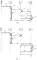
- the device has started in the usual operating mode, but the auxiliary processor 10 is in the state. abnormal operating condition. This situation is illustrated by the sequence diagram of the Fig. 7 .
- sequencer 35 waits for components of the device to be operational.
- step 312 sequencer 35 attempts to start auxiliary processor 10 and, in step 313, initiates delayed start of main processor 50.
- auxiliary processor 10 remains blocked due to the startup software disabled.
- the starting of the main processor 50 then takes place by order of the sequencer 35, in step 319, at the end of the predefined delay already mentioned. This delay is set so that the time elapsed since the start of the auxiliary processor 10 by the sequencer 35 is greater than the time required, in normal operating state, for the auxiliary processor 10 to be able to receive the first synchronization message transmitted by the processor. main 50.
- main processor 50 sends the first synchronization message to auxiliary processor 10 and, in step 317, activates the watchdog.
- the auxiliary processor 10 is not in the normal operating state and does not respond to the first synchronization message.
- the main processor 50 finds that the auxiliary processor 10 is not in the normal operating state, that is to say that the auxiliary processor 10 is not operational.
- the main processor 50 in a step 321, then switches the auxiliary processor 10 into the update mode, and proceeds to update the start-up software, as already described in relation with the Figs. 2 and 3 .
- the device whose behavior is described above includes mechanisms for updating the startup software without increasing the necessary resources of the device and in particular the capacity of the rewritable non-volatile memory used to store the startup software.
- a corruption of stored data or instructions remains possible by an unfortunate writing in the rewritable non-volatile memory 12.
- standby mode is meant for example a mode in which only the auxiliary processor 10 operates and the components not essential for the operation of the auxiliary processor 10 are then not. powered.
- the algorithm of the Fig. 5 shows a 300 extinguishing procedure.
- a step 301 the main processor 50 verifies the integrity of the start-up software present in the rewritable non-volatile memory 12.
- a step 302 the main processor 50 tests the result of the verification. If the validity test is positive, a step 305 is performed. Otherwise, the validity test is negative, thus revealing a corruption of the startup software present in the rewritable non-volatile memory 12, and the main processor 50 performs a step 303.
- step 303 the main processor 50 performs the phase of updating the start-up software, as already described in relation to the Fig. 2 , then step 305 is performed.
- step 305 the main processor 50 turns off the device and the algorithm is terminated.
Landscapes
- Engineering & Computer Science (AREA)
- Theoretical Computer Science (AREA)
- General Engineering & Computer Science (AREA)
- Software Systems (AREA)
- Physics & Mathematics (AREA)
- General Physics & Mathematics (AREA)
- Computer Security & Cryptography (AREA)
- Quality & Reliability (AREA)
- Stored Programmes (AREA)
- Power Sources (AREA)
- Retry When Errors Occur (AREA)
- Hardware Redundancy (AREA)
- Multi Processors (AREA)
Claims (7)
- Aktualisierungsverfahren einer Startsoftware, die in einem wiederbeschreibbaren nichtflüchtigen Speicher (12) einer Vorrichtung gespeichert ist, die einen ersten Prozessor (10) und einen zweiten Prozessor (50) enthält, wobei der erste Prozessor (10) die Startsoftware ausführen kann, wobei das Verfahren von der Vorrichtung durchgeführt wird und dadurch gekennzeichnet ist, dass das Verfahren eine verzögerte Startphase des zweiten Prozessors (50) bezüglich des Starts des ersten Prozessors (10) aufweist, damit:- wenn die Startsoftware nicht gültig ist, die Vorrichtung in einem Aktualisierungsmodus der Startsoftware startet und der erste Prozessor (10) aufgrund dessen blockiert ist, dass die Startsoftware ungültig gemacht wurde, und der zweite Prozessor (50) beim Start überprüft, ob der erste Prozessor (10) Nachrichtenaustauschvorgänge ausführt, um den ersten (10) und den zweiten (50) Prozessor zu synchronisieren, und, wenn der zweite Prozessor (50) keine Nachricht vom ersten Prozessor (10) empfängt, der zweite Prozessor (50) den Aktualisierungsmodus der Startsoftware auslöst; und- wenn die Startsoftware gültig ist, die Vorrichtung mit der Startsoftware derart startet, dass der erste Prozessor (10) mit der Startsoftware startet und die Startsoftware vom ersten Prozessor (10) fordert, den zweiten Prozessor (50) zu starten und sich durch die Nachrichtenaustauschvorgänge zu synchronisieren.
- Verfahren nach Anspruch 1, dadurch gekennzeichnet, dass die vom zweiten Prozessor (50) durchgeführte Aktualisierung der Startsoftware die folgenden Schritte enthält:- Umschalten (101) des ersten Prozessors in den Aktualisierungsmodus der Startsoftware;- Schreiben (102) einer neuen Startsoftware in den wiederbeschreibbaren nichtflüchtigen Speicher;- Überprüfen (103), ob die neue Startsoftware, wie sie in den wiederbeschreibbaren nichtflüchtigen Speicher geschrieben wurde, gültig ist;- Wiederholen der Aktualisierung in dem Schritt, der darin besteht, die neue Startsoftware zu schreiben, wenn die wie geschriebene neue Startsoftware nicht gültig ist; und- Umschalten (105) des ersten Prozessors (10) in einen üblichen Betriebsmodus, wenn die neue Software wie geschrieben gültig ist.
- Verfahren nach einem der Ansprüche 1 und 2, dadurch gekennzeichnet, dass der zweite Prozessor (50) zur Überprüfung des Betriebszustands des ersten Prozessors (10) die folgenden Schritte ausführt:- Senden einer ersten Nachricht an den ersten Prozessor (10);- Betrachten des Betriebszustands des ersten Prozessors (10) als normal, wenn der zweite Prozessor (50) eine zweite Nachricht empfängt, die die erste Nachricht in einer vordefinierten Frist quittiert; und- Betrachten des Betriebszustands des ersten Prozessors (10) als anormal, wenn der zweite Prozessor (50) die zweite Nachricht, die die erste Nachricht quittiert, nicht in der vordefinierten Frist empfängt.
- Verfahren nach einem der Ansprüche 1 bis 3, dadurch gekennzeichnet, dass es außerdem beim Ausschalten der Vorrichtung die folgenden Schritte enthält:- Überprüfen (301), ob die im wiederbeschreibbaren nichtflüchtigen Speicher gespeicherte Startsoftware gültig ist; und- Starten (303) der Aktualisierung der Startsoftware mit Hilfe des zweiten Prozessors (50), wenn die im wiederbeschreibbaren nichtflüchtigen Speicher gespeicherte Startsoftware nicht gültig ist.
- Computerprogrammprodukt, das Anweisungen aufweist, um durch erste (10) und zweite (50) Prozessoren das Verfahren nach einem der Ansprüche 1 bis 4 zu implementieren, wenn die Anweisungen von den ersten (10) und zweiten (50) Prozessoren ausgeführt werden.
- Computerlesbarer Speicherträger, der ein Computerprogrammprodukt nach Anspruch 5 speichert.
- Vorrichtung, die einen ersten Prozessor (10) und einen zweiten Prozessor (50) enthält, wobei der erste Prozessor eine in einem wiederbeschreibbaren nichtflüchtigen Speicher gespeicherte Startsoftware ausführen kann, wobei die Vorrichtung dadurch gekennzeichnet ist, dass sie Einrichtungen aufweist, um eine verzögerte Startphase des zweiten Prozessors (50) bezüglich des Starts des ersten Prozessors (10) auszuführen, damit:- wenn die Startsoftware nicht gültig ist, die Vorrichtung Einrichtungen aufweist, um in einem Aktualisierungsmodus der Startsoftware zu starten, wobei der erste Prozessor (10) konfiguriert ist, aufgrund dessen blockiert zu werden, dass die Startsoftware ungültig gemacht wurde, und der zweite Prozessor (50) konfiguriert ist, beim Start zu überprüfen, ob der erste Prozessor (10) Nachrichtenaustauschvorgänge ausführt, um den ersten (10) und den zweiten (50) Prozessor zu synchronisieren, und, wenn der zweite Prozessor (50) keine Nachricht vom ersten Prozessor (10) empfängt, der zweite Prozessor (50) Einrichtungen aufweist, um den Aktualisierungsmodus der Startsoftware auszulösen; und- wenn die Startsoftware gültig ist, die Vorrichtung Einrichtungen aufweist, um mit der Startsoftware derart zu starten, dass der erste Prozessor (10) mit der Startsoftware startet und die Startsoftware vom ersten Prozessor (10) fordert, den zweiten Prozessor (50) zu starten und sich durch die NachrichtenAustauschvorgänge zu synchronisieren.
Applications Claiming Priority (3)
| Application Number | Priority Date | Filing Date | Title |
|---|---|---|---|
| FR1358710A FR3010553B1 (fr) | 2013-09-10 | 2013-09-10 | Procede de mise a jour d'un logiciel de demarrage d'un dispositif multiprocesseur |
| EP14761841.7A EP3044679B1 (de) | 2013-09-10 | 2014-09-09 | Verfahren zur aktualisierung eines startladers einer multiprozessorvorrichtung |
| PCT/EP2014/069157 WO2015036388A1 (fr) | 2013-09-10 | 2014-09-09 | Procédé de mise à jour d'un logiciel de démarrage d'un dispositif multiprocesseur |
Related Parent Applications (2)
| Application Number | Title | Priority Date | Filing Date |
|---|---|---|---|
| EP14761841.7A Division EP3044679B1 (de) | 2013-09-10 | 2014-09-09 | Verfahren zur aktualisierung eines startladers einer multiprozessorvorrichtung |
| EP14761841.7A Division-Into EP3044679B1 (de) | 2013-09-10 | 2014-09-09 | Verfahren zur aktualisierung eines startladers einer multiprozessorvorrichtung |
Publications (2)
| Publication Number | Publication Date |
|---|---|
| EP3540602A1 EP3540602A1 (de) | 2019-09-18 |
| EP3540602B1 true EP3540602B1 (de) | 2020-12-16 |
Family
ID=50023663
Family Applications (2)
| Application Number | Title | Priority Date | Filing Date |
|---|---|---|---|
| EP14761841.7A Active EP3044679B1 (de) | 2013-09-10 | 2014-09-09 | Verfahren zur aktualisierung eines startladers einer multiprozessorvorrichtung |
| EP19164830.2A Active EP3540602B1 (de) | 2013-09-10 | 2014-09-09 | Aktualisierungsverfahren einer einschaltsoftware einer multiprozessorvorrichtung |
Family Applications Before (1)
| Application Number | Title | Priority Date | Filing Date |
|---|---|---|---|
| EP14761841.7A Active EP3044679B1 (de) | 2013-09-10 | 2014-09-09 | Verfahren zur aktualisierung eines startladers einer multiprozessorvorrichtung |
Country Status (6)
| Country | Link |
|---|---|
| US (2) | US10289422B2 (de) |
| EP (2) | EP3044679B1 (de) |
| CN (2) | CN110069363B (de) |
| BR (1) | BR112016005213B1 (de) |
| FR (1) | FR3010553B1 (de) |
| WO (1) | WO2015036388A1 (de) |
Families Citing this family (9)
| Publication number | Priority date | Publication date | Assignee | Title |
|---|---|---|---|---|
| DE102017125172A1 (de) * | 2017-10-26 | 2019-05-02 | Schréder S.A. | Verfahren zur Aktualisierung eines Bootloaders eines Controllers einer Leuchte |
| CN107704258B (zh) * | 2017-10-27 | 2020-12-01 | 深圳市恒扬数据股份有限公司 | Uboot升级方法、系统及终端设备 |
| US10901479B1 (en) | 2019-04-23 | 2021-01-26 | Motorola Solutions, Inc. | Method and apparatus for managing power-up of a portable communication device |
| US12050692B2 (en) * | 2019-10-30 | 2024-07-30 | John A. Nix | Secure and flexible boot firmware update for devices with a primary platform |
| US11374877B2 (en) * | 2020-03-16 | 2022-06-28 | Hewlett Packard Enterprise Development Lp | Runtime schema for services in a switch |
| US11321077B1 (en) * | 2020-06-05 | 2022-05-03 | Amazon Technologies, Inc. | Live updating of firmware behavior |
| US12056497B2 (en) * | 2021-02-03 | 2024-08-06 | Ampere Computing Llc | Multi-socket computing system employing a parallelized boot architecture with partially concurrent processor boot-up operations, and related methods |
| US11797679B2 (en) * | 2021-07-28 | 2023-10-24 | Dell Products, L.P. | Trust verification system and method for a baseboard management controller (BMC) |
| JP2023105421A (ja) * | 2022-01-19 | 2023-07-31 | キヤノン株式会社 | 情報処理装置および情報処理装置の制御方法 |
Family Cites Families (32)
| Publication number | Priority date | Publication date | Assignee | Title |
|---|---|---|---|---|
| EP1475704A2 (de) * | 2003-05-08 | 2004-11-10 | Matsushita Electric Industrial Co., Ltd. | Informationsverarbeitungsgerät |
| KR100506203B1 (ko) * | 2003-09-17 | 2005-08-05 | 삼성전자주식회사 | 부팅 및 부트 코드 업데이트 방법 및 시스템 |
| KR100987628B1 (ko) * | 2004-02-07 | 2010-10-13 | 엘지전자 주식회사 | 엠비디드 컨트롤러의 펌웨어 갱신방법 및 갱신용 펌웨어저장매체 |
| US7574590B2 (en) * | 2005-10-26 | 2009-08-11 | Sigmatel, Inc. | Method for booting a system on a chip integrated circuit |
| US7600055B2 (en) * | 2006-01-03 | 2009-10-06 | International Business Machines Corporation | Apparatus, system, and method for firmware update of redundant controllers |
| JP4868216B2 (ja) * | 2006-01-19 | 2012-02-01 | 日本電気株式会社 | ファームウェア更新回路およびファームウェア更新方法 |
| JP2007206885A (ja) * | 2006-01-31 | 2007-08-16 | Toshiba Corp | コンピュータシステム及びシステム起動方法 |
| US7870379B2 (en) * | 2006-10-10 | 2011-01-11 | Exaflop Llc | Updating a power supply microcontroller |
| US8320302B2 (en) * | 2007-04-20 | 2012-11-27 | Elster Electricity, Llc | Over the air microcontroller flash memory updates |
| CN101815988A (zh) * | 2007-10-04 | 2010-08-25 | 无极公司 | 固件映像更新和管理 |
| EP2310941A1 (de) * | 2008-06-02 | 2011-04-20 | Awox | Verfahren und einrichtung zum aktualisieren einer computeranwendung |
| CN101739270B (zh) * | 2008-11-05 | 2013-04-03 | 英华达(上海)科技有限公司 | 电子装置及其系统更新方法 |
| US20100131694A1 (en) * | 2008-11-26 | 2010-05-27 | Kelly Scott G | Secure Boot ROM Emulation |
| US9077654B2 (en) * | 2009-10-30 | 2015-07-07 | Iii Holdings 2, Llc | System and method for data center security enhancements leveraging managed server SOCs |
| US8417962B2 (en) * | 2010-06-11 | 2013-04-09 | Microsoft Corporation | Device booting with an initial protection component |
| US8713559B2 (en) * | 2010-11-15 | 2014-04-29 | Schneider Electric It Corporation | System and method for updating firmware |
| GB2501433B (en) * | 2011-01-19 | 2014-06-04 | Ibm | Ensuring the integrity of software |
| KR20120092222A (ko) * | 2011-02-11 | 2012-08-21 | 삼성전자주식회사 | 보안 부팅 방법 및 보안 부트 이미지 생성 방법 |
| US8578362B2 (en) * | 2011-03-18 | 2013-11-05 | Hamilton Sundstrand Corporation | Method for downloading software to an electronics product |
| US8707019B2 (en) * | 2011-07-02 | 2014-04-22 | Intel Corporation | Component update using management engine |
| CN103010039A (zh) * | 2011-09-28 | 2013-04-03 | 宁波拜特测控技术有限公司 | 一种电池管理系统引导加载方法 |
| US9274805B2 (en) * | 2012-02-24 | 2016-03-01 | Qualcomm Incorporated | System and method for thermally aware device booting |
| CN102780578A (zh) * | 2012-05-29 | 2012-11-14 | 上海斐讯数据通信技术有限公司 | 网络设备的操作系统的更新系统及更新方法 |
| US8442792B1 (en) * | 2012-10-26 | 2013-05-14 | Elbex Video Ltd. | Method and apparatus for calibrating intelligent AC outlets |
| KR20140060912A (ko) * | 2012-11-13 | 2014-05-21 | 한국전자통신연구원 | 부트로더를 업데이트하는 방법 및 장치 |
| US9021457B2 (en) * | 2013-01-22 | 2015-04-28 | Apple Inc. | Method and system for dynamically resizing enclosed storage device partitions |
| US9336010B2 (en) * | 2013-03-15 | 2016-05-10 | Xilinx, Inc. | Multi-boot or fallback boot of a system-on-chip using a file-based boot device |
| US9292301B1 (en) * | 2015-04-06 | 2016-03-22 | Psikick, Inc. | Systems, methods, and apparatus for controlling the power-on or boot sequence of an integrated circuit based on power harvesting conditions |
| US10002015B2 (en) * | 2015-07-10 | 2018-06-19 | International Business Machines Corporation | Delayed boot of a virtual machine in a virtualized computing environment based on a fabric limit |
| US9858067B2 (en) * | 2015-10-05 | 2018-01-02 | Samsung Electronics Co., Ltd. | Electronic system with update control mechanism and method of operation thereof |
| US10496388B2 (en) * | 2016-03-24 | 2019-12-03 | Intel Corporation | Technologies for securing a firmware update |
| US10452404B2 (en) * | 2016-07-28 | 2019-10-22 | Microsoft Technology Licensing, Llc. | Optimized UEFI reboot process |
-
2013
- 2013-09-10 FR FR1358710A patent/FR3010553B1/fr not_active Expired - Fee Related
-
2014
- 2014-09-09 CN CN201910260833.4A patent/CN110069363B/zh not_active Expired - Fee Related
- 2014-09-09 US US14/917,710 patent/US10289422B2/en active Active
- 2014-09-09 EP EP14761841.7A patent/EP3044679B1/de active Active
- 2014-09-09 BR BR112016005213-7A patent/BR112016005213B1/pt active IP Right Grant
- 2014-09-09 EP EP19164830.2A patent/EP3540602B1/de active Active
- 2014-09-09 CN CN201480058518.9A patent/CN105683921B/zh not_active Expired - Fee Related
- 2014-09-09 WO PCT/EP2014/069157 patent/WO2015036388A1/fr not_active Ceased
-
2019
- 2019-03-29 US US16/370,194 patent/US11061690B2/en active Active
Non-Patent Citations (1)
| Title |
|---|
| None * |
Also Published As
| Publication number | Publication date |
|---|---|
| CN105683921A (zh) | 2016-06-15 |
| FR3010553B1 (fr) | 2015-09-04 |
| US20160216978A1 (en) | 2016-07-28 |
| EP3044679A1 (de) | 2016-07-20 |
| CN110069363B (zh) | 2023-05-12 |
| US10289422B2 (en) | 2019-05-14 |
| EP3044679B1 (de) | 2019-05-15 |
| FR3010553A1 (fr) | 2015-03-13 |
| CN110069363A (zh) | 2019-07-30 |
| US20190227811A1 (en) | 2019-07-25 |
| WO2015036388A1 (fr) | 2015-03-19 |
| EP3540602A1 (de) | 2019-09-18 |
| US11061690B2 (en) | 2021-07-13 |
| CN105683921B (zh) | 2019-04-23 |
| BR112016005213B1 (pt) | 2021-01-26 |
Similar Documents
| Publication | Publication Date | Title |
|---|---|---|
| EP3044679B1 (de) | Verfahren zur aktualisierung eines startladers einer multiprozessorvorrichtung | |
| US10701084B2 (en) | Reliable and secure firmware update with a dynamic validation for internet of things (IoT) devices | |
| CN105122262B (zh) | 辅助非易失性存储器中的冗余系统引导代码 | |
| US20100306544A1 (en) | Secure computing environment in a transportable container | |
| EP2100250B1 (de) | System und verfahren zur datensicherung | |
| EP1764694B1 (de) | Redundanzkontrollverfahren und Vorrichtung für sichere Rechnereinheiten | |
| CN111722960A (zh) | 一种cmos信息异常下的开机方法、系统、设备以及介质 | |
| FR3072195A1 (fr) | Procede de gestion d'un retour de produit pour analyse et produit correspondant | |
| EP2498184A1 (de) | Vorrichtung zur Verbesserung der Fehlertoleranz eines Prozessors | |
| CN114444083A (zh) | 一种基于bmc的服务器bios全生命周期安全保护系统 | |
| JP2011076295A (ja) | 組込系コントローラ | |
| JP5818257B2 (ja) | 計算機システム、電源切断処理装置、電源切断処理方法およびプログラム | |
| JP6310914B2 (ja) | バックアップ制御装置及びバックアップ制御方法 | |
| CN111427721A (zh) | 异常恢复方法及装置 | |
| EP1632837A1 (de) | Verfahren zum Konfigurieren eines Mikrokontroller Systemtaktes | |
| CN119248360B (zh) | 休眠流程中镜像异常恢复方法、装置及存储介质 | |
| WO2026013349A1 (fr) | Contrôle de l'état de santé d'une réserve d'énergie d'un calculateur | |
| FR2965949A1 (fr) | Procede de sauvegarde optimisee de donnees dans la memoire d'un calculateur equipant un vehicule automobile | |
| JP3087650B2 (ja) | 自動復電方式 | |
| WO2007104899A1 (fr) | Procede de mise a jour robuste de logiciel | |
| CN121326357A (zh) | 系统升级方法以及分布式系统 | |
| FR2956913A1 (fr) | Procede de sequencement deterministe multitache | |
| FR2868563A1 (fr) | Dispositif et procede capables de detecter un etat du bois en vue de regler une horloge | |
| FR3104278A1 (fr) | Système informatique embarqué à bord d'un porteur mettant en oeuvre au moins un service critique pour la sûreté de fonctionnement du porteur | |
| FR3003052A1 (fr) | Procede et dispositif de gestion de quorums de nœuds de groupes a haute disponibilite d'un calculateur haute performance |
Legal Events
| Date | Code | Title | Description |
|---|---|---|---|
| PUAI | Public reference made under article 153(3) epc to a published international application that has entered the european phase |
Free format text: ORIGINAL CODE: 0009012 |
|
| STAA | Information on the status of an ep patent application or granted ep patent |
Free format text: STATUS: THE APPLICATION HAS BEEN PUBLISHED |
|
| AC | Divisional application: reference to earlier application |
Ref document number: 3044679 Country of ref document: EP Kind code of ref document: P |
|
| AK | Designated contracting states |
Kind code of ref document: A1 Designated state(s): AL AT BE BG CH CY CZ DE DK EE ES FI FR GB GR HR HU IE IS IT LI LT LU LV MC MK MT NL NO PL PT RO RS SE SI SK SM TR |
|
| STAA | Information on the status of an ep patent application or granted ep patent |
Free format text: STATUS: REQUEST FOR EXAMINATION WAS MADE |
|
| 17P | Request for examination filed |
Effective date: 20200309 |
|
| RBV | Designated contracting states (corrected) |
Designated state(s): AL AT BE BG CH CY CZ DE DK EE ES FI FR GB GR HR HU IE IS IT LI LT LU LV MC MK MT NL NO PL PT RO RS SE SI SK SM TR |
|
| GRAP | Despatch of communication of intention to grant a patent |
Free format text: ORIGINAL CODE: EPIDOSNIGR1 |
|
| STAA | Information on the status of an ep patent application or granted ep patent |
Free format text: STATUS: GRANT OF PATENT IS INTENDED |
|
| INTG | Intention to grant announced |
Effective date: 20200703 |
|
| GRAS | Grant fee paid |
Free format text: ORIGINAL CODE: EPIDOSNIGR3 |
|
| GRAA | (expected) grant |
Free format text: ORIGINAL CODE: 0009210 |
|
| STAA | Information on the status of an ep patent application or granted ep patent |
Free format text: STATUS: THE PATENT HAS BEEN GRANTED |
|
| AC | Divisional application: reference to earlier application |
Ref document number: 3044679 Country of ref document: EP Kind code of ref document: P |
|
| AK | Designated contracting states |
Kind code of ref document: B1 Designated state(s): AL AT BE BG CH CY CZ DE DK EE ES FI FR GB GR HR HU IE IS IT LI LT LU LV MC MK MT NL NO PL PT RO RS SE SI SK SM TR |
|
| REG | Reference to a national code |
Ref country code: GB Ref legal event code: FG4D Free format text: NOT ENGLISH |
|
| REG | Reference to a national code |
Ref country code: IE Ref legal event code: FG4D Free format text: LANGUAGE OF EP DOCUMENT: FRENCH |
|
| REG | Reference to a national code |
Ref country code: DE Ref legal event code: R096 Ref document number: 602014073509 Country of ref document: DE |
|
| REG | Reference to a national code |
Ref country code: AT Ref legal event code: REF Ref document number: 1346214 Country of ref document: AT Kind code of ref document: T Effective date: 20210115 |
|
| PG25 | Lapsed in a contracting state [announced via postgrant information from national office to epo] |
Ref country code: NO Free format text: LAPSE BECAUSE OF FAILURE TO SUBMIT A TRANSLATION OF THE DESCRIPTION OR TO PAY THE FEE WITHIN THE PRESCRIBED TIME-LIMIT Effective date: 20210316 Ref country code: GR Free format text: LAPSE BECAUSE OF FAILURE TO SUBMIT A TRANSLATION OF THE DESCRIPTION OR TO PAY THE FEE WITHIN THE PRESCRIBED TIME-LIMIT Effective date: 20210317 Ref country code: RS Free format text: LAPSE BECAUSE OF FAILURE TO SUBMIT A TRANSLATION OF THE DESCRIPTION OR TO PAY THE FEE WITHIN THE PRESCRIBED TIME-LIMIT Effective date: 20201216 Ref country code: FI Free format text: LAPSE BECAUSE OF FAILURE TO SUBMIT A TRANSLATION OF THE DESCRIPTION OR TO PAY THE FEE WITHIN THE PRESCRIBED TIME-LIMIT Effective date: 20201216 |
|
| REG | Reference to a national code |
Ref country code: AT Ref legal event code: MK05 Ref document number: 1346214 Country of ref document: AT Kind code of ref document: T Effective date: 20201216 |
|
| REG | Reference to a national code |
Ref country code: NL Ref legal event code: MP Effective date: 20201216 |
|
| PG25 | Lapsed in a contracting state [announced via postgrant information from national office to epo] |
Ref country code: BG Free format text: LAPSE BECAUSE OF FAILURE TO SUBMIT A TRANSLATION OF THE DESCRIPTION OR TO PAY THE FEE WITHIN THE PRESCRIBED TIME-LIMIT Effective date: 20210316 Ref country code: LV Free format text: LAPSE BECAUSE OF FAILURE TO SUBMIT A TRANSLATION OF THE DESCRIPTION OR TO PAY THE FEE WITHIN THE PRESCRIBED TIME-LIMIT Effective date: 20201216 Ref country code: SE Free format text: LAPSE BECAUSE OF FAILURE TO SUBMIT A TRANSLATION OF THE DESCRIPTION OR TO PAY THE FEE WITHIN THE PRESCRIBED TIME-LIMIT Effective date: 20201216 |
|
| PG25 | Lapsed in a contracting state [announced via postgrant information from national office to epo] |
Ref country code: NL Free format text: LAPSE BECAUSE OF FAILURE TO SUBMIT A TRANSLATION OF THE DESCRIPTION OR TO PAY THE FEE WITHIN THE PRESCRIBED TIME-LIMIT Effective date: 20201216 Ref country code: HR Free format text: LAPSE BECAUSE OF FAILURE TO SUBMIT A TRANSLATION OF THE DESCRIPTION OR TO PAY THE FEE WITHIN THE PRESCRIBED TIME-LIMIT Effective date: 20201216 |
|
| REG | Reference to a national code |
Ref country code: LT Ref legal event code: MG9D |
|
| PG25 | Lapsed in a contracting state [announced via postgrant information from national office to epo] |
Ref country code: SK Free format text: LAPSE BECAUSE OF FAILURE TO SUBMIT A TRANSLATION OF THE DESCRIPTION OR TO PAY THE FEE WITHIN THE PRESCRIBED TIME-LIMIT Effective date: 20201216 Ref country code: SM Free format text: LAPSE BECAUSE OF FAILURE TO SUBMIT A TRANSLATION OF THE DESCRIPTION OR TO PAY THE FEE WITHIN THE PRESCRIBED TIME-LIMIT Effective date: 20201216 Ref country code: EE Free format text: LAPSE BECAUSE OF FAILURE TO SUBMIT A TRANSLATION OF THE DESCRIPTION OR TO PAY THE FEE WITHIN THE PRESCRIBED TIME-LIMIT Effective date: 20201216 Ref country code: CZ Free format text: LAPSE BECAUSE OF FAILURE TO SUBMIT A TRANSLATION OF THE DESCRIPTION OR TO PAY THE FEE WITHIN THE PRESCRIBED TIME-LIMIT Effective date: 20201216 Ref country code: LT Free format text: LAPSE BECAUSE OF FAILURE TO SUBMIT A TRANSLATION OF THE DESCRIPTION OR TO PAY THE FEE WITHIN THE PRESCRIBED TIME-LIMIT Effective date: 20201216 Ref country code: PT Free format text: LAPSE BECAUSE OF FAILURE TO SUBMIT A TRANSLATION OF THE DESCRIPTION OR TO PAY THE FEE WITHIN THE PRESCRIBED TIME-LIMIT Effective date: 20210416 Ref country code: RO Free format text: LAPSE BECAUSE OF FAILURE TO SUBMIT A TRANSLATION OF THE DESCRIPTION OR TO PAY THE FEE WITHIN THE PRESCRIBED TIME-LIMIT Effective date: 20201216 |
|
| PG25 | Lapsed in a contracting state [announced via postgrant information from national office to epo] |
Ref country code: AT Free format text: LAPSE BECAUSE OF FAILURE TO SUBMIT A TRANSLATION OF THE DESCRIPTION OR TO PAY THE FEE WITHIN THE PRESCRIBED TIME-LIMIT Effective date: 20201216 Ref country code: PL Free format text: LAPSE BECAUSE OF FAILURE TO SUBMIT A TRANSLATION OF THE DESCRIPTION OR TO PAY THE FEE WITHIN THE PRESCRIBED TIME-LIMIT Effective date: 20201216 |
|
| REG | Reference to a national code |
Ref country code: DE Ref legal event code: R097 Ref document number: 602014073509 Country of ref document: DE |
|
| PG25 | Lapsed in a contracting state [announced via postgrant information from national office to epo] |
Ref country code: IS Free format text: LAPSE BECAUSE OF FAILURE TO SUBMIT A TRANSLATION OF THE DESCRIPTION OR TO PAY THE FEE WITHIN THE PRESCRIBED TIME-LIMIT Effective date: 20210416 |
|
| PLBE | No opposition filed within time limit |
Free format text: ORIGINAL CODE: 0009261 |
|
| STAA | Information on the status of an ep patent application or granted ep patent |
Free format text: STATUS: NO OPPOSITION FILED WITHIN TIME LIMIT |
|
| PG25 | Lapsed in a contracting state [announced via postgrant information from national office to epo] |
Ref country code: IT Free format text: LAPSE BECAUSE OF FAILURE TO SUBMIT A TRANSLATION OF THE DESCRIPTION OR TO PAY THE FEE WITHIN THE PRESCRIBED TIME-LIMIT Effective date: 20201216 Ref country code: AL Free format text: LAPSE BECAUSE OF FAILURE TO SUBMIT A TRANSLATION OF THE DESCRIPTION OR TO PAY THE FEE WITHIN THE PRESCRIBED TIME-LIMIT Effective date: 20201216 |
|
| 26N | No opposition filed |
Effective date: 20210917 |
|
| PG25 | Lapsed in a contracting state [announced via postgrant information from national office to epo] |
Ref country code: DK Free format text: LAPSE BECAUSE OF FAILURE TO SUBMIT A TRANSLATION OF THE DESCRIPTION OR TO PAY THE FEE WITHIN THE PRESCRIBED TIME-LIMIT Effective date: 20201216 |
|
| PG25 | Lapsed in a contracting state [announced via postgrant information from national office to epo] |
Ref country code: ES Free format text: LAPSE BECAUSE OF FAILURE TO SUBMIT A TRANSLATION OF THE DESCRIPTION OR TO PAY THE FEE WITHIN THE PRESCRIBED TIME-LIMIT Effective date: 20201216 |
|
| PG25 | Lapsed in a contracting state [announced via postgrant information from national office to epo] |
Ref country code: SI Free format text: LAPSE BECAUSE OF FAILURE TO SUBMIT A TRANSLATION OF THE DESCRIPTION OR TO PAY THE FEE WITHIN THE PRESCRIBED TIME-LIMIT Effective date: 20201216 |
|
| REG | Reference to a national code |
Ref country code: CH Ref legal event code: PL |
|
| REG | Reference to a national code |
Ref country code: BE Ref legal event code: MM Effective date: 20210930 |
|
| PG25 | Lapsed in a contracting state [announced via postgrant information from national office to epo] |
Ref country code: IS Free format text: LAPSE BECAUSE OF FAILURE TO SUBMIT A TRANSLATION OF THE DESCRIPTION OR TO PAY THE FEE WITHIN THE PRESCRIBED TIME-LIMIT Effective date: 20210416 Ref country code: MC Free format text: LAPSE BECAUSE OF FAILURE TO SUBMIT A TRANSLATION OF THE DESCRIPTION OR TO PAY THE FEE WITHIN THE PRESCRIBED TIME-LIMIT Effective date: 20201216 |
|
| PG25 | Lapsed in a contracting state [announced via postgrant information from national office to epo] |
Ref country code: LU Free format text: LAPSE BECAUSE OF NON-PAYMENT OF DUE FEES Effective date: 20210909 Ref country code: IE Free format text: LAPSE BECAUSE OF NON-PAYMENT OF DUE FEES Effective date: 20210909 Ref country code: BE Free format text: LAPSE BECAUSE OF NON-PAYMENT OF DUE FEES Effective date: 20210930 |
|
| PG25 | Lapsed in a contracting state [announced via postgrant information from national office to epo] |
Ref country code: LI Free format text: LAPSE BECAUSE OF NON-PAYMENT OF DUE FEES Effective date: 20210930 Ref country code: CH Free format text: LAPSE BECAUSE OF NON-PAYMENT OF DUE FEES Effective date: 20210930 |
|
| PG25 | Lapsed in a contracting state [announced via postgrant information from national office to epo] |
Ref country code: CY Free format text: LAPSE BECAUSE OF FAILURE TO SUBMIT A TRANSLATION OF THE DESCRIPTION OR TO PAY THE FEE WITHIN THE PRESCRIBED TIME-LIMIT Effective date: 20201216 |
|
| PG25 | Lapsed in a contracting state [announced via postgrant information from national office to epo] |
Ref country code: HU Free format text: LAPSE BECAUSE OF FAILURE TO SUBMIT A TRANSLATION OF THE DESCRIPTION OR TO PAY THE FEE WITHIN THE PRESCRIBED TIME-LIMIT; INVALID AB INITIO Effective date: 20140909 |
|
| PG25 | Lapsed in a contracting state [announced via postgrant information from national office to epo] |
Ref country code: MK Free format text: LAPSE BECAUSE OF FAILURE TO SUBMIT A TRANSLATION OF THE DESCRIPTION OR TO PAY THE FEE WITHIN THE PRESCRIBED TIME-LIMIT Effective date: 20201216 |
|
| PG25 | Lapsed in a contracting state [announced via postgrant information from national office to epo] |
Ref country code: TR Free format text: LAPSE BECAUSE OF FAILURE TO SUBMIT A TRANSLATION OF THE DESCRIPTION OR TO PAY THE FEE WITHIN THE PRESCRIBED TIME-LIMIT Effective date: 20201216 |
|
| PG25 | Lapsed in a contracting state [announced via postgrant information from national office to epo] |
Ref country code: MT Free format text: LAPSE BECAUSE OF FAILURE TO SUBMIT A TRANSLATION OF THE DESCRIPTION OR TO PAY THE FEE WITHIN THE PRESCRIBED TIME-LIMIT Effective date: 20201216 |
|
| PGFP | Annual fee paid to national office [announced via postgrant information from national office to epo] |
Ref country code: DE Payment date: 20250820 Year of fee payment: 12 |
|
| PGFP | Annual fee paid to national office [announced via postgrant information from national office to epo] |
Ref country code: GB Payment date: 20250822 Year of fee payment: 12 |
|
| PGFP | Annual fee paid to national office [announced via postgrant information from national office to epo] |
Ref country code: FR Payment date: 20250821 Year of fee payment: 12 |