EP3535844B1 - Oring-steuerung mit niedrigspannungsvorrichtung für hochspannungs-gleichstromrack - Google Patents
Oring-steuerung mit niedrigspannungsvorrichtung für hochspannungs-gleichstromrack Download PDFInfo
- Publication number
- EP3535844B1 EP3535844B1 EP17787994.7A EP17787994A EP3535844B1 EP 3535844 B1 EP3535844 B1 EP 3535844B1 EP 17787994 A EP17787994 A EP 17787994A EP 3535844 B1 EP3535844 B1 EP 3535844B1
- Authority
- EP
- European Patent Office
- Prior art keywords
- mosfet
- voltage
- comparator
- power supply
- condition
- Prior art date
- Legal status (The legal status is an assumption and is not a legal conclusion. Google has not performed a legal analysis and makes no representation as to the accuracy of the status listed.)
- Active
Links
Images



Classifications
-
- H—ELECTRICITY
- H02—GENERATION; CONVERSION OR DISTRIBUTION OF ELECTRIC POWER
- H02H—EMERGENCY PROTECTIVE CIRCUIT ARRANGEMENTS
- H02H3/00—Emergency protective circuit arrangements for automatic disconnection directly responsive to an undesired change from normal electric working condition with or without subsequent reconnection ; integrated protection
- H02H3/26—Emergency protective circuit arrangements for automatic disconnection directly responsive to an undesired change from normal electric working condition with or without subsequent reconnection ; integrated protection responsive to difference between voltages or between currents; responsive to phase angle between voltages or between currents
- H02H3/28—Emergency protective circuit arrangements for automatic disconnection directly responsive to an undesired change from normal electric working condition with or without subsequent reconnection ; integrated protection responsive to difference between voltages or between currents; responsive to phase angle between voltages or between currents involving comparison of the voltage or current values at two spaced portions of a single system, e.g. at opposite ends of one line, at input and output of apparatus
-
- H—ELECTRICITY
- H02—GENERATION; CONVERSION OR DISTRIBUTION OF ELECTRIC POWER
- H02J—ELECTRIC POWER NETWORKS; CIRCUIT ARRANGEMENTS OR SYSTEMS FOR SUPPLYING OR DISTRIBUTING ELECTRIC POWER; SYSTEMS FOR STORING ELECTRIC ENERGY
- H02J1/00—Circuit arrangements for DC mains or DC distribution networks
- H02J1/06—Two-wire DC power distribution systems
-
- G—PHYSICS
- G06—COMPUTING OR CALCULATING; COUNTING
- G06F—ELECTRIC DIGITAL DATA PROCESSING
- G06F1/00—Details not covered by groups G06F3/00 - G06F13/00 and G06F21/00
- G06F1/26—Power supply means, e.g. regulation thereof
-
- H—ELECTRICITY
- H02—GENERATION; CONVERSION OR DISTRIBUTION OF ELECTRIC POWER
- H02H—EMERGENCY PROTECTIVE CIRCUIT ARRANGEMENTS
- H02H9/00—Emergency protective circuit arrangements for limiting excess current or voltage without disconnection
- H02H9/005—Emergency protective circuit arrangements for limiting excess current or voltage without disconnection avoiding undesired transient conditions
-
- H—ELECTRICITY
- H02—GENERATION; CONVERSION OR DISTRIBUTION OF ELECTRIC POWER
- H02H—EMERGENCY PROTECTIVE CIRCUIT ARRANGEMENTS
- H02H9/00—Emergency protective circuit arrangements for limiting excess current or voltage without disconnection
- H02H9/04—Emergency protective circuit arrangements for limiting excess current or voltage without disconnection responsive to excess voltage
-
- H—ELECTRICITY
- H03—ELECTRONIC CIRCUITRY
- H03K—PULSE TECHNIQUE
- H03K17/00—Electronic switching or gating, i.e. not by contact-making and –breaking
- H03K17/08—Modifications for protecting switching circuit against overcurrent or overvoltage
- H03K17/081—Modifications for protecting switching circuit against overcurrent or overvoltage without feedback from the output circuit to the control circuit
- H03K17/0812—Modifications for protecting switching circuit against overcurrent or overvoltage without feedback from the output circuit to the control circuit by measures taken in the control circuit
- H03K17/08122—Modifications for protecting switching circuit against overcurrent or overvoltage without feedback from the output circuit to the control circuit by measures taken in the control circuit in field-effect transistor switches
Definitions
- Server systems that provide Internet-based services typically rely on racks to house and supply power to the load devices that provide such services.
- the load devices used in these racks such as power conversion devices, motherboards, processing chips (e.g., central processing units, graphical processing units, etc.), network switches, accelerators, etc., may become more and more powerful.
- processing chips e.g., central processing units, graphical processing units, etc.
- network switches e.g., central processing units, graphical processing units, etc.
- accelerators e.g., accelerators, etc.
- V DC direct current
- each rack receives 48V DC to supply power to the load devices.
- the maximum power is around tens of kilowatts (kW).
- kW kilowatts
- these 48V DC power systems may no longer be sufficient to bring power to the trays of the racks.
- the higher input voltage to the rack for distribution to the trays the more power can deliver with the same amount of copper for bus bars of these racks.
- High voltage power supply systems such as 400V DC
- 400V DC allow for greater power distribution and fewer stages of power conversions for 12V powered server computing devices as compared to 48Vdc. This greater power also creates greater efficiency in the system with ten times the power capacity for the same structural power supply (bus bar).
- 400V DC distribution racks are becoming more and more appealing to Internet technology companies such as those that provide cloud-based processing and storage solutions.
- Document US 2015/016005 A1 refers to a system for supplying power from an input node to a load coupled to an output node.
- the system may have multiple switches coupled between the input node and the output node.
- One or more limiting circuits may be configured for controlling the switches so as to limit outputs of the switches. For example, the limiting circuits may limit current through the respective switches.
- One or more timers may set a delay period for indicating a fault condition after the limiting is initiated.
- Enhancement-mode MOSFET 120 includes a drain coupled to a first node, a source coupled to a second node, and a gate.
- Amplifier 50 includes inputs for comparing the voltages from the first and second nodes and an output coupled to the gate of MOSFET 120 by which amplifier 50 controls the state of enhancement-mode MOSFET 120.
- Amplifier 50 further includes a positive power input coupled to the second node and a negative power input coupled to ground.
- the first node is operable to be coupled to a power supply 10 and the second node is operable to be coupled to a load 18.
- One aspect of the disclosure provides a system for protecting server racks connected to a power supply.
- the system includes an Oring circuit including a first MOSFET, a first diode connected in parallel with the first MOSFET, and first and second comparators operatively coupled to the first MOSFET.
- Each of the first and second comparators support a maximum voltage difference that is less than an operational voltage of the power supply.
- the system also includes a clamping circuit including a second MOSFET and a second diode operatively coupled to the Oring circuit.
- Each of the first and second comparators is configured to compare voltage at the first MOSFET with voltage at the second MOSFET.
- the first comparator is configured to switch the first MOSFET to an off condition according to the compared voltage and the second comparator is configured to switch the first MOSFET to an on condition according to the compared voltage.
- the second MOSFET is configured to clamp a node of the first comparator and a node of the second comparator to below the maximum voltage difference when there is a short at the power supply.
- each of the first and second comparators support voltages of no more than 20V.
- the system also includes a server rack.
- an operational voltage of the power supply when the power supply supplies power to operate computing components of the server rack is greater than 48V. In such examples, the operational voltage of the power supply when the power supply supplies power to operate computing components of the server rack is 400V.
- the second diode is a Schottky diode configured to clamp transient spikes.
- the system also includes the power supply.
- the system also includes a Hotswap controller configured with a third MOSFET such that the third MOSFET is arranged with the Oring circuit and clamping circuit to disconnect a load from the power supply when there is a load side short of the system.
- the clamping circuit further includes a resistor that limits current from the power supply to the second MOSFET.
- the Oring circuit also includes a third diode configured as a single sided hysteresis clamping diode.
- the Oring circuit also includes first and second resistors such that the third diode and the first and second resistors are arranged to reduce a voltage value of a threshold of the first comparator when the first MOSFET is switched to the on condition.
- the first comparator is arranged to have a first threshold for switching the first MOSFET to the on condition when the first MOSFET is operating in a linear region or in the off condition, and the first comparator has a second threshold for keeping the first MOSFET in the on condition when the first MOSFET is already operating in the on condition.
- the first threshold is a greater voltage than the second threshold.
- the second comparator has a single voltage threshold for switching the first MOSFET to the off condition, such that when voltage at the second MOSFET is greater than the single voltage threshold, the second comparator will cause the first MOSFET to switch to the off condition.
- the protection circuit includes an Oring circuit including a first MOSFET, a first diode connected in parallel with the first MOSFET, and first and second comparators operatively coupled to the first MOSFET. Each of the first and second comparators support a maximum voltage difference that is less than an operational voltage of the power supply.
- the protection circuit also includes a clamping circuit including a second MOSFET and a second diode operatively coupled to the Oring circuit, and a Hotswap controller configured with a third MOSFET.
- Third MOSFET is arranged with the Oring circuit and clamping circuit to disconnect a load from the power supply when there is a load side short of the protection circuit.
- Each of the first and second comparators are configured to compare voltage at the first MOSFET with voltage at the second MOSFET.
- the first comparator is configured to switch the first MOSFET to an off condition according to the compared voltage and the second comparator is configured to switch the first MOSFET to an on condition according to the compared voltage.
- the second MOSFET is configured to clamp a node of the first comparator and a node of the second comparator to below the maximum voltage difference when there is a short at the power supply.
- each of the first and second comparators supports voltages of less than 20V.
- the second diode is a Schottky diode that clamps transient spikes.
- the clamping circuit further includes a resistor which limits current from the power supply to the second MOSFET.
- the Oring circuit also includes a third diode configured as a single sided hysteresis clamping diode D3.
- the Oring circuit also includes first and second resistors such that the third diode and the first and second resistors are arranged to reduce a voltage value of a threshold of the first comparator when the first MOSFET is switched to the on condition.
- the first comparator is arranged to have a first threshold for switching the first MOSFET to the on condition when the first MOSFET is operating in a linear region or in the off condition, and the first comparator has a second threshold for keeping the first MOSFET in the on condition when the first MOSFET is already operating in the on condition.
- the first threshold is a greater voltage than the second threshold.
- the systems and protecting circuits according to the aspects, examples and embodiments described herein are provided to, at least in part, ensure safe and reliable function of the racks as well as protecting components of the systems and protecting circuits from being damaged.
- each rack may include a protection circuit that includes hotswap and Oring functionality.
- the protection circuit may include an Oring circuit including a Oring metal-oxide semiconductor field effect transistor ("MOSFET”) switch and a diode connected in parallel with the MOSFET.
- MOSFET has an on condition, a linear mode, and an off condition.
- the Oring MOSFET will be conducted via a body diode (of the MOSFET) and eventually turned to the on condition.
- a hotswap MOSFET When a short occurs at a load side of the protection circuit from which the load devices receive power, a hotswap MOSFET will be switched to the off condition.
- an Oring controller When an input short occurs at the input side of the protection circuit, where the power supply system provides power to the protection circuit, an Oring controller will sense a negative or reverse current flow, switching the Oring MOSFET to the off condition immediately so that holdup capacitor energy can be reserved for the load devices.
- a high common voltage difference amplifier may be arranged on the "high" or input side of a protection circuit to sense current flowing through an Oring MOSFET.
- the high common voltage difference amplifier can be an expensive component, and during normal operation using a high voltage power supply, if the input side has a short, the drain of the Oring MOSFET will see the high voltage of the power supply and the source of the Oring MOSFET will see very low voltage.
- the differential voltage at the amplifier can be as high as the voltage of the high voltage power supply, potentially resulting in damage to the protection circuit.
- a low common voltage differential amplifier may be used on the low side of a protection circuit to sense the current flowing through the Oring MOSFET. This will require that the comparator is referred to the output ground load. As such, when the input side has a short and the source voltage of the Oring MOSFET is very low, the high voltage of the power supply will be applied to the drain of the Oring MOSFET, which again may result in damage to the protection circuit. In addition, this is only feasible for low side sensing.
- a clamping circuit and an additional low common voltage differential amplifier may be included with the Oring circuit in the protection circuit.
- the clamping circuit may include an additional MOSFET, a resistor and a diode.
- Each of the low common voltage differential amplifiers may include a comparator operatively coupled to the first MOSFET and that supports a maximum difference that is less than the operational voltage of the power supply.
- the additional MOSFET may acts to clamp one of the nodes of each of the amplifiers so that when the input side of the protection circuit has as short, the voltage on those nodes will be clamped to below the maximum rating of the amplifier.
- This additional MOSFET may be arranged in parallel with the Oring MOSFET such that the additional MOSFET acts as a source follower. During normal operation, the Oring MOSFET and the additional MOSFET will be in the on condition.
- the pair of amplifiers may be used for detecting two events: 1) a large positive voltage during reverse conduction and 2) a large negative voltage during start up.
- Each amplifier receives the source voltage for each of the Oring and additional MOSFET.
- One of the amplifiers uses the comparison of these voltages to turn the Oring MOSFET to the on condition.
- This amplifier is arranged with a single sided hysteresis clamping diode for one-direction hysteresis.
- the other amplifier is configured to turn the Oring MOSFET to the off condition based on the comparison.
- a protection circuit for server racks may include an Oring circuit having a first MOSFET, a first diode, and first and second comparators. Each of the first and second comparators supports a maximum voltage difference that is less than an operational voltage of the power supply.
- the protection circuit also includes a clamping circuit having a second MOSFET and a second diode.
- Each of the first and second comparators is configured to compare voltage at the first MOSFET with voltage at the second MOSFET.
- the first comparator is configured to switch the first MOSFET to an off condition using the comparison
- the second comparator is configured to switch the first MOSFET to an on condition using the comparison.
- the second MOSFET is configured to clamp a node of each of the first and second comparators to below the maximum in the event of a short at the power supply.
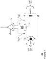
- a high common voltage differential amplifier 110 may be used.
- the high common voltage difference amplifier 110 is arranged on the input or "high" side 120 to sense current flowing through an Oring circuit including an Oring MOSFET 130 and a diode 132 connected in parallel with the Oring MOSFET.
- the voltage to the protection circuit at the input side 120 is 400V.
- the high common voltage difference amplifier 110 can be an expensive component, and during normal operation, if the input side has a short, the drain 140 of the Oring MOSFET M3 will see 400V. At the same time, the source 142 will see very low voltage (i.e., close to zero). As a result, the differential voltage on the high common voltage difference amplifier 110 will be as much as 400V, potentially resulting in damage to the protection circuit 100.
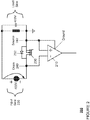
- a low common voltage differential amplifier 210 may be used as shown in FIGURE 2 on the low side to sense the current flowing through an Oring circuit including Oring MOSFET 230 and a diode 232 connected in parallel the Oring MOSFET.
- the low common voltage differential amplifier 210 may be, for example, a comparator that supports differential voltages of less than 20V such as a commercially available LT1018 comparator. This will require that the comparator 210 is connected to the output ground load.
- the output 400V will be applied to the drain 140 of the Oring MOSFET 230. Accordingly, as with the example of protection circuit 100, there will be still high voltage across the comparator 210, resulting in damage to the system. In addition, this is only feasible for low side sensing.
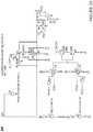
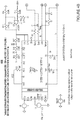
- FIGURES 3A and 3B depict an example configuration of a protection circuit 300 for high side sensing with a pair of low common voltage difference amplifiers or comparators U1 and U2, an Oring circuit (including an Oring MOSFET M3 and a diode 308 connected in parallel with the Oring MOSFET), and a clamping circuit. Protection circuit 300 will be described with regard to FIGURE 3A , although FIGURE 3B provides additional example implementation details.
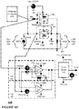
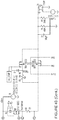
- FIGURES 4A and 4B depict an example of the protection circuit 300 of FIGURES 3A and 3B depicted with a Hotswap circuit including a Hotswap controller such as a commercially available LT9100 Hotswap controller.
- M3 is an Oring MOSFET as described above.
- the clamping circuit includes an additional MOSFET M2, resistor R8 and diode D1.
- M2 acts to clamp the Vsense nodes 310, 312 of the comparators U1, U2 so that when the input side 320 has as short, the voltage on the Vsense nodes will be clamped to below the maximum rating of the comparator. In other words, the voltage to the comparators will not exceed the maximum voltage or Vcc_COMP of the comparators.
- M2 is connected in parallel with M3, and as such, the M2 forms a source follower. Thus, when the drain of M2 sees a higher voltage, the current flows through the channel and raises the voltage at the source 342 to roughly Vcc_COMP-Vth, where Vcc_COMP is the fixed gate voltage and the Vth is the threshold of the MOSFET.
- M2 will be in the linear mode and the current will be limited by the resistor R8.
- D1 may be an ultrafast or Schottky diode which clamps fast transient spikes.
- M3 will be switched to the on condition and the voltage across M2 will be very low, for example 0.2V or more or less. Accordingly, M2 will be switched to the on condition as well, since the gate voltage at the M2 (Vgs) is at Vcc_COMP (5V), and the current flow through M2 will be very small, roughly 350uA.
- the voltage across M2 is very low or 350uA ⁇ Rdon ⁇ 1mV, allowing the protection circuit 300 to use the differential voltage between Vsense (the voltage at Vsense 344) and Vsource (the voltage at the source 342 of M3) to sense the voltage across M3.
- Comparators U1 and U2 may be window comparators (such as LT1018) used for detecting two events: 1) a big positive voltage during reverse conduction and 2) a big negative voltage during start up.
- U1 is arranged with a single sided hysteresis clamping diode D3 for one-direction hysteresis.
- the comparator U1 is configured to turn M3 to the on condition based on the differential voltage between Vsense and Vsource, while the comparator Us is configured to turn M3 to the off condition based upon the differential voltage between Vsense and Vsource.
- the body diode of M2 will be on initially and the comparator U1 should sense ⁇ 1V. This will cause the gate driver 350 to turn M3 to the on condition.
- the comparator U1 has a low output, there is no hysteresis. If the Vsense is lower than the threshold V7 (for example if Vsense is -0.7V) and assuming the source of M3 is 0 potential, the comparator U1 outputs high which causes the gate driver 350 to turn M3 to the on condition to reduce the conduction loss. At this point, the body diode of the M3 and external diode D2 may both conduct. While the comparator U1 outputs high, there will be feedback from the output Vcc_COMP through D3 to the non-inverting node 420 of the comparator U1.
- the sensed voltage Vsense (Ids*Rdson) will be lower ( ⁇ -0.2V).
- the threshold for turning on M3 must be lowered by the one directional hysteresis. So D3 is helpful to increase the voltage on the non-inverting node 420 and hold M3 in the on condition.
- Vsense is higher than -(V7-(Vcc_COMP-VF) ⁇ R9 ⁇ (R10+R9)
- M3 will be switched to the off condition, where VF is the diode voltage drop of D3.
- Comparator U2 may set a threshold (V2) for reverse current protection. When the Vsense is higher than Vsource + V2 at comparator U2, the gate driver 350 will cause M3 to be switched to the off condition.
- the comparator U2 When an overload occurs at the load side 322, the comparator U2 will sense a high current which can be used to control a Hotswap circuit in order to protect the input side 320.
- the protection circuit 300 may be utilized with a Hotswap controller 410, an example implementation is shown in detail in FIGURE 4B .
- FIGURE 5 is an example of waveforms of protection circuit 400 in a rack at 0A loading for the example sequence of initialization (t0), ramp up (t1), steady state (t2, normal operation), input short (t3-t4), restart (t5) ramp up (t6), steady state (t7), and output short (t8).
- the internal control voltage source for example Vcc_COMP and Vcc_GateDrive are ramping up to a valid value.
- the hotswap or input is connected to the protection circuit, so current starts to flow via D2 and/or D1.
- Vgs of M2 will be roughly Vcc_COMP (5V), and M2 will be turned to the on condition by the gate driver. So the sensed voltage difference of Source and Vsense (Source-Vsense) is roughly equal to the voltage difference between Source and Drain of M3.
- Vsource-Vsense will be around IV, which will be higher than V7.
- U3 will output high and the gate of M3 will also be high.
- the on threshold of M3 will be reduced to a lower level, as shown by the dashed line 510 of FIGURE 5 . This will help the M3 to stay in the on condition.
- the differential voltage, Vsource-Vsense is the drain current of the MOSFET times the resistance of the MOSFET in the on condition or Ids*Rdson, which is ⁇ 1V.
- Vin voltage into the protection circuit from the load side 320
- Vout voltage out to the load devices on the load side 330
- the input side 320 has a short event (input short), so initially, the holdup capacitor 360 on the load side 322 will charge via M2.
- the differential voltage (Vsource-Vsense) is negative, and U2 will output low right away, causing the gate driver 350 to switch M3 to the off condition.
- the absolute value of the differential voltage (Vsource-Vsense) remains below a few volts, e.g., less than about 2.5 volts or more or less6.
- the short is cleared (power is restored via the power source) and the rack is restarted at t5. Thereafter, between t5 to t8, the rack operates as between t0 up until t3. However, at t8, a short on the load side occurs and is shortly thereafter cleared. The short on the load side causes the Hotswap MOSFET M1 (See FIGURE 4B ) to be switched to the off condition, disconnecting the protection circuit from the input.
- clamping circuit described above and shown in the figures is depicted in a particular configuration, there is merely one example arrangement of a MOSFET, resistor and diode which can be used as a clamping circuit.
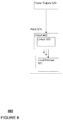
- FIGURE 6 is an example of a system 600 including protection circuit 400 (protection circuit 300 with hotswap) as discussed above (or at least protection circuit 300 without the hotswap).
- the system 600 includes a rack 610 and a power supply 620.
- power supply 620 may provide greater than 48V DC, such as 400V or even greater voltages.
- Within the rack is a set of one or more load devices 630 which are connected to protection circuit 400.
- the load devices power conversion devices, motherboards, processing chips, network switches, accelerators, and any other devices which utilize power provided by the protection circuit 400.
- the arrows of FIGURE 6 represent optimal directions of current flow.
- the protection circuit 400 may connect and disconnect the load devices 630 to the power supply 620 safely (via the Hotswap controller 410) and at the same time provide both input side and low side sensing.
- the features described herein utilize Hotswap and Oring functions to prevent undesired interference to a high voltage DC bus.
- a low common voltage difference amplifier can be used without high side current sensing circuitry, reducing costs and simplifying implementation.
- a low voltage integrated circuit ⁇ 20V
- ⁇ 20V can be used to resolve the problems of a high voltage DC (at 20x higher voltage level), saving significantly in implementation costs for each server tray in the rack.
- the configurations discussed herein allow for both high side and low side Oring control with a Hotswap.
- the configurations can be used for very high power racks without affecting the costs of the power distribution system.
- additional savings may also be expected in terms of size (physical space required to house the racks and components within the racks), energy needed for cooling as the system is more efficient, density within the racks as more devices can be supported by the same rack, costs of bus bar copper, etc.
- the present technology enjoys wide industrial applicability including, but not limited to, server systems utilizing high voltage power systems.
Landscapes
- Engineering & Computer Science (AREA)
- Power Engineering (AREA)
- Theoretical Computer Science (AREA)
- Physics & Mathematics (AREA)
- General Engineering & Computer Science (AREA)
- General Physics & Mathematics (AREA)
- Emergency Protection Circuit Devices (AREA)
- Electronic Switches (AREA)
Claims (13)
- Ein System zum Schutz von Server-Racks, die mit einer Stromversorgung verbunden sind, wobei das System Folgendes umfasst:eine ORing-Schaltung mit einem ersten MOSFET (M3), einer ersten Diode (D2), die parallel zu dem ersten MOSFET geschaltet ist, und einem ersten und einem zweiten Komparator (U1, U2), die mit dem ersten MOSFET (M3) und einem zweiten MOSFET (M2) gekoppelt sind, wobei sowohl der erste als auch der zweite Komparator eine maximale Spannungsdifferenz unterstützen, die kleiner als eine Betriebsspannung der Stromversorgung ist; undeine Klemmschaltung mit dem zweiten MOSFET (M2) und einer zweiten Diode (D1), die mit der ORing-Schaltung gekoppelt ist, undwobei sowohl der erste als auch der zweite Komparator so konfiguriert sind, dass sie eine Quellenspannung an dem ersten MOSFET mit einer Quellenspannung an dem zweiten MOSFET vergleichen, wobei der erste Komparator (U2) so konfiguriert ist, dass er den ersten MOSFET entsprechend der verglichenen Spannung in einen Aus-Zustand schaltet und der zweite Komparator (U1) so konfiguriert ist, dass er den ersten MOSFET entsprechend der verglichenen Spannung in einen Ein-Zustand schaltet, wobei der zweite MOSFET so konfiguriert ist, dass er einen Knoten des ersten Komparators und einen Knoten des zweiten Komparators unter der maximalen Spannungsdifferenz hält, wenn ein Kurzschluss an der Stromversorgung auftritt.
- System nach Anspruch 1, wobei sowohl der erste als auch der zweite Komparator Spannungen von nicht mehr als 20V unterstützen.
- System nach Anspruch 2, ferner ein Servergestell umfassend.
- System nach Anspruch 3, bei dem die Betriebsspannung der Stromversorgung, wenn die Stromversorgung Strom zum Betrieb von Rechenkomponenten des Serverschranks liefert, größer als 48 V ist.
- System nach Anspruch 4, bei dem die Betriebsspannung der Stromversorgung, wenn die Stromversorgung Strom zum Betreiben von Rechenkomponenten des Serverschranks liefert, 400 V beträgt.
- System nach Anspruch 1, bei dem die zweite Diode eine Schottky-Diode ist, die so konfiguriert ist, dass sie vorübergehende Spitzen klemmt.
- System nach Anspruch 6, das ferner die Stromversorgung umfasst.
- System nach Anspruch 1, ferner umfassend einen Hotswap-Controller, der mit einem dritten MOSFET konfiguriert ist, so dass der dritte MOSFET mit der ORing-Schaltung und der Klemmschaltung angeordnet ist, um eine Last von der Stromversorgung zu trennen, wenn eine Lastseite des Systems kurzgeschlossen ist.
- System nach Anspruch 1, wobei die Klemmschaltung ferner einen Widerstand enthält, der den Strom von der Stromversorgung zum zweiten MOSFET begrenzt.
- System nach Anspruch 1, bei dem die ORing-Schaltung ferner eine dritte Diode enthält, die als einseitige Hysterese-Klemmdiode konfiguriert ist.
- System nach Anspruch 10, wobei die ORing-Schaltung ferner einen ersten und einen zweiten Widerstand enthält, so dass die dritte Diode und der erste und der zweite Widerstand so angeordnet sind, dass sie einen Spannungswert einer Schwelle des ersten Komparators reduzieren, wenn der erste MOSFET in den Einschaltzustand geschaltet wird.
- System nach Anspruch 11, wobei der erste Komparator so angeordnet ist, dass er einen ersten Schwellenwert zum Schalten des ersten MOSFET in den Ein-Zustand hat, wenn der erste MOSFET in einem linearen Bereich oder im Aus-Zustand arbeitet, und wobei der erste Komparator einen zweiten Schwellenwert hat, um den ersten MOSFET im Ein-Zustand zu halten, wenn der erste MOSFET bereits im Ein-Zustand arbeitet, wobei der erste Schwellenwert eine größere Spannung als der zweite Schwellenwert ist.
- System nach Anspruch 12, bei dem der zweite Komparator einen einzelnen Spannungsschwellenwert zum Schalten des ersten MOSFET in den Aus-Zustand aufweist, so dass, wenn die Spannung am zweiten MOSFET größer als der einzelne Spannungsschwellenwert ist, der zweite Komparator den ersten MOSFET veranlasst, in den Aus-Zustand zu schalten.
Applications Claiming Priority (2)
| Application Number | Priority Date | Filing Date | Title |
|---|---|---|---|
| US15/375,833 US10381822B2 (en) | 2016-12-12 | 2016-12-12 | Oring control using low voltage device for high voltage DC rack |
| PCT/US2017/053941 WO2018111375A1 (en) | 2016-12-12 | 2017-09-28 | Oring control using low voltage device for high voltage dc rack |
Publications (2)
| Publication Number | Publication Date |
|---|---|
| EP3535844A1 EP3535844A1 (de) | 2019-09-11 |
| EP3535844B1 true EP3535844B1 (de) | 2020-09-09 |
Family
ID=60162246
Family Applications (1)
| Application Number | Title | Priority Date | Filing Date |
|---|---|---|---|
| EP17787994.7A Active EP3535844B1 (de) | 2016-12-12 | 2017-09-28 | Oring-steuerung mit niedrigspannungsvorrichtung für hochspannungs-gleichstromrack |
Country Status (5)
| Country | Link |
|---|---|
| US (1) | US10381822B2 (de) |
| EP (1) | EP3535844B1 (de) |
| DE (1) | DE202017105775U1 (de) |
| DK (1) | DK3535844T3 (de) |
| WO (1) | WO2018111375A1 (de) |
Families Citing this family (4)
| Publication number | Priority date | Publication date | Assignee | Title |
|---|---|---|---|---|
| JP2019068662A (ja) * | 2017-10-03 | 2019-04-25 | 株式会社オートネットワーク技術研究所 | 電源供給システム |
| CN110098648B (zh) * | 2019-04-24 | 2023-07-07 | 青岛海洋科技中心 | 用于海洋观探测浮标的能源管理系统 |
| TWM595928U (zh) * | 2020-02-18 | 2020-05-21 | 力智電子股份有限公司 | 電源開關電路 |
| US20240429817A1 (en) * | 2023-06-20 | 2024-12-26 | Delta Electronics, Inc. | Power supply unit and power supply system with same |
Family Cites Families (11)
| Publication number | Priority date | Publication date | Assignee | Title |
|---|---|---|---|---|
| JPS5954319A (ja) | 1982-09-22 | 1984-03-29 | Matsushita Electric Ind Co Ltd | コンパレ−タ |
| US7269034B2 (en) | 1997-01-24 | 2007-09-11 | Synqor, Inc. | High efficiency power converter |
| EP0954899A2 (de) | 1997-01-24 | 1999-11-10 | Fische, LLC | Hocheffizienter stromrichter |
| US5945816A (en) | 1998-04-21 | 1999-08-31 | Alcatel Network Systems, Inc. | Self-biased power isolator system |
| US6894468B1 (en) | 1999-07-07 | 2005-05-17 | Synqor, Inc. | Control of DC/DC converters having synchronous rectifiers |
| US7206800B1 (en) | 2000-08-30 | 2007-04-17 | Micron Technology, Inc. | Overflow detection and clamping with parallel operand processing for fixed-point multipliers |
| US7379282B1 (en) * | 2002-12-26 | 2008-05-27 | Network Appliance, Inc | Input and output isolating diode for power dissipation reduction of power supplies |
| US7466573B2 (en) | 2006-05-16 | 2008-12-16 | Honeywell International, Inc. | Method and apparatus for integrated active-diode-ORing and soft power switching |
| US7760479B2 (en) * | 2008-04-09 | 2010-07-20 | Fairchild Semiconductor Corporation | Technique for combining in-rush current limiting and short circuit current limiting |
| US9621020B2 (en) | 2008-05-16 | 2017-04-11 | Astec International Limited | Control circuits and methods for controlling switching devices |
| US10003190B2 (en) | 2013-07-12 | 2018-06-19 | Linear Technology Corporation | Inrush control with multiple switches |
-
2016
- 2016-12-12 US US15/375,833 patent/US10381822B2/en active Active
-
2017
- 2017-09-22 DE DE202017105775.5U patent/DE202017105775U1/de active Active
- 2017-09-28 WO PCT/US2017/053941 patent/WO2018111375A1/en not_active Ceased
- 2017-09-28 DK DK17787994.7T patent/DK3535844T3/da active
- 2017-09-28 EP EP17787994.7A patent/EP3535844B1/de active Active
Non-Patent Citations (1)
| Title |
|---|
| None * |
Also Published As
| Publication number | Publication date |
|---|---|
| DK3535844T3 (da) | 2020-11-30 |
| DE202017105775U1 (de) | 2017-12-20 |
| US20180166873A1 (en) | 2018-06-14 |
| US10381822B2 (en) | 2019-08-13 |
| EP3535844A1 (de) | 2019-09-11 |
| WO2018111375A1 (en) | 2018-06-21 |
Similar Documents
| Publication | Publication Date | Title |
|---|---|---|
| EP3535844B1 (de) | Oring-steuerung mit niedrigspannungsvorrichtung für hochspannungs-gleichstromrack | |
| US8278997B1 (en) | Apparatus and methodology for controlling hot swap MOSFETs | |
| US9024609B2 (en) | Circuit and method for providing hold-up time in a DC-DC converter | |
| US8395917B2 (en) | Redundant parallel non-isolated input converters | |
| EP3086459B1 (de) | Leistungswandlervorrichtung | |
| RU2642839C2 (ru) | Высоковольтный преобразователь постоянного напряжения в постоянное напряжение | |
| US20150207307A1 (en) | Boost apparatus with over-current and over-voltage protection function | |
| US9041433B2 (en) | System and method for driving transistors | |
| US20200091704A1 (en) | Power conversion system with abnormal energy protection and method of operating the same | |
| TW201508296A (zh) | 檢測在熱切換應用中的故障 | |
| US20170040999A1 (en) | Auxiliary commutated silicon-controlled rectifier circuit methods and systems | |
| US9966776B2 (en) | Discharge of back-up capacitor by constant current | |
| US20180143263A1 (en) | Current restriction | |
| US8400745B1 (en) | Fuse apparatus | |
| US20160301387A1 (en) | Active filtering system | |
| CN112350288A (zh) | 用于热插拔控制器的通信端子 | |
| US9673692B2 (en) | Application of normally closed power semiconductor devices | |
| US11095118B2 (en) | Controlled holdup discharge for improved component reliability | |
| TWI638501B (zh) | Redundant power supply system that extends the hold time after power failure | |
| JP2002215273A (ja) | 電源システム及び活線挿抜方法 | |
| JP7783064B2 (ja) | 電源遮断保護回路、電源遮断保護回路の制御方法、電源遮断保護コントローラ、データ記憶装置 | |
| WO2016085460A1 (en) | Switch between first power source and second power source | |
| EP2932801B1 (de) | Elektronische schaltung zum schutz einer last vor überspannung | |
| US20190058402A1 (en) | Short-circuit protected power supply circuit | |
| KR102088890B1 (ko) | 양방향 dc-dc 컨버터의 보호 장치 및 방법 |
Legal Events
| Date | Code | Title | Description |
|---|---|---|---|
| STAA | Information on the status of an ep patent application or granted ep patent |
Free format text: STATUS: UNKNOWN |
|
| STAA | Information on the status of an ep patent application or granted ep patent |
Free format text: STATUS: THE INTERNATIONAL PUBLICATION HAS BEEN MADE |
|
| PUAI | Public reference made under article 153(3) epc to a published international application that has entered the european phase |
Free format text: ORIGINAL CODE: 0009012 |
|
| STAA | Information on the status of an ep patent application or granted ep patent |
Free format text: STATUS: REQUEST FOR EXAMINATION WAS MADE |
|
| 17P | Request for examination filed |
Effective date: 20190603 |
|
| AK | Designated contracting states |
Kind code of ref document: A1 Designated state(s): AL AT BE BG CH CY CZ DE DK EE ES FI FR GB GR HR HU IE IS IT LI LT LU LV MC MK MT NL NO PL PT RO RS SE SI SK SM TR |
|
| AX | Request for extension of the european patent |
Extension state: BA ME |
|
| DAV | Request for validation of the european patent (deleted) | ||
| DAX | Request for extension of the european patent (deleted) | ||
| GRAP | Despatch of communication of intention to grant a patent |
Free format text: ORIGINAL CODE: EPIDOSNIGR1 |
|
| STAA | Information on the status of an ep patent application or granted ep patent |
Free format text: STATUS: GRANT OF PATENT IS INTENDED |
|
| INTG | Intention to grant announced |
Effective date: 20200402 |
|
| GRAS | Grant fee paid |
Free format text: ORIGINAL CODE: EPIDOSNIGR3 |
|
| GRAA | (expected) grant |
Free format text: ORIGINAL CODE: 0009210 |
|
| STAA | Information on the status of an ep patent application or granted ep patent |
Free format text: STATUS: THE PATENT HAS BEEN GRANTED |
|
| AK | Designated contracting states |
Kind code of ref document: B1 Designated state(s): AL AT BE BG CH CY CZ DE DK EE ES FI FR GB GR HR HU IE IS IT LI LT LU LV MC MK MT NL NO PL PT RO RS SE SI SK SM TR |
|
| REG | Reference to a national code |
Ref country code: GB Ref legal event code: FG4D |
|
| REG | Reference to a national code |
Ref country code: AT Ref legal event code: REF Ref document number: 1312826 Country of ref document: AT Kind code of ref document: T Effective date: 20200915 Ref country code: CH Ref legal event code: EP |
|
| REG | Reference to a national code |
Ref country code: DE Ref legal event code: R096 Ref document number: 602017023438 Country of ref document: DE |
|
| REG | Reference to a national code |
Ref country code: IE Ref legal event code: FG4D |
|
| REG | Reference to a national code |
Ref country code: CH Ref legal event code: NV Representative=s name: RENTSCH PARTNER AG, CH |
|
| REG | Reference to a national code |
Ref country code: NL Ref legal event code: FP |
|
| REG | Reference to a national code |
Ref country code: DK Ref legal event code: T3 Effective date: 20201124 |
|
| REG | Reference to a national code |
Ref country code: SE Ref legal event code: TRGR |
|
| REG | Reference to a national code |
Ref country code: FI Ref legal event code: FGE |
|
| REG | Reference to a national code |
Ref country code: LT Ref legal event code: MG4D |
|
| PG25 | Lapsed in a contracting state [announced via postgrant information from national office to epo] |
Ref country code: HR Free format text: LAPSE BECAUSE OF FAILURE TO SUBMIT A TRANSLATION OF THE DESCRIPTION OR TO PAY THE FEE WITHIN THE PRESCRIBED TIME-LIMIT Effective date: 20200909 Ref country code: LT Free format text: LAPSE BECAUSE OF FAILURE TO SUBMIT A TRANSLATION OF THE DESCRIPTION OR TO PAY THE FEE WITHIN THE PRESCRIBED TIME-LIMIT Effective date: 20200909 Ref country code: NO Free format text: LAPSE BECAUSE OF FAILURE TO SUBMIT A TRANSLATION OF THE DESCRIPTION OR TO PAY THE FEE WITHIN THE PRESCRIBED TIME-LIMIT Effective date: 20201209 Ref country code: GR Free format text: LAPSE BECAUSE OF FAILURE TO SUBMIT A TRANSLATION OF THE DESCRIPTION OR TO PAY THE FEE WITHIN THE PRESCRIBED TIME-LIMIT Effective date: 20201210 Ref country code: BG Free format text: LAPSE BECAUSE OF FAILURE TO SUBMIT A TRANSLATION OF THE DESCRIPTION OR TO PAY THE FEE WITHIN THE PRESCRIBED TIME-LIMIT Effective date: 20201209 |
|
| REG | Reference to a national code |
Ref country code: AT Ref legal event code: MK05 Ref document number: 1312826 Country of ref document: AT Kind code of ref document: T Effective date: 20200909 |
|
| PG25 | Lapsed in a contracting state [announced via postgrant information from national office to epo] |
Ref country code: RS Free format text: LAPSE BECAUSE OF FAILURE TO SUBMIT A TRANSLATION OF THE DESCRIPTION OR TO PAY THE FEE WITHIN THE PRESCRIBED TIME-LIMIT Effective date: 20200909 Ref country code: LV Free format text: LAPSE BECAUSE OF FAILURE TO SUBMIT A TRANSLATION OF THE DESCRIPTION OR TO PAY THE FEE WITHIN THE PRESCRIBED TIME-LIMIT Effective date: 20200909 Ref country code: PL Free format text: LAPSE BECAUSE OF FAILURE TO SUBMIT A TRANSLATION OF THE DESCRIPTION OR TO PAY THE FEE WITHIN THE PRESCRIBED TIME-LIMIT Effective date: 20200909 |
|
| PG25 | Lapsed in a contracting state [announced via postgrant information from national office to epo] |
Ref country code: EE Free format text: LAPSE BECAUSE OF FAILURE TO SUBMIT A TRANSLATION OF THE DESCRIPTION OR TO PAY THE FEE WITHIN THE PRESCRIBED TIME-LIMIT Effective date: 20200909 Ref country code: CZ Free format text: LAPSE BECAUSE OF FAILURE TO SUBMIT A TRANSLATION OF THE DESCRIPTION OR TO PAY THE FEE WITHIN THE PRESCRIBED TIME-LIMIT Effective date: 20200909 Ref country code: RO Free format text: LAPSE BECAUSE OF FAILURE TO SUBMIT A TRANSLATION OF THE DESCRIPTION OR TO PAY THE FEE WITHIN THE PRESCRIBED TIME-LIMIT Effective date: 20200909 Ref country code: PT Free format text: LAPSE BECAUSE OF FAILURE TO SUBMIT A TRANSLATION OF THE DESCRIPTION OR TO PAY THE FEE WITHIN THE PRESCRIBED TIME-LIMIT Effective date: 20210111 Ref country code: SM Free format text: LAPSE BECAUSE OF FAILURE TO SUBMIT A TRANSLATION OF THE DESCRIPTION OR TO PAY THE FEE WITHIN THE PRESCRIBED TIME-LIMIT Effective date: 20200909 |
|
| PG25 | Lapsed in a contracting state [announced via postgrant information from national office to epo] |
Ref country code: IS Free format text: LAPSE BECAUSE OF FAILURE TO SUBMIT A TRANSLATION OF THE DESCRIPTION OR TO PAY THE FEE WITHIN THE PRESCRIBED TIME-LIMIT Effective date: 20210109 Ref country code: AT Free format text: LAPSE BECAUSE OF FAILURE TO SUBMIT A TRANSLATION OF THE DESCRIPTION OR TO PAY THE FEE WITHIN THE PRESCRIBED TIME-LIMIT Effective date: 20200909 Ref country code: AL Free format text: LAPSE BECAUSE OF FAILURE TO SUBMIT A TRANSLATION OF THE DESCRIPTION OR TO PAY THE FEE WITHIN THE PRESCRIBED TIME-LIMIT Effective date: 20200909 Ref country code: ES Free format text: LAPSE BECAUSE OF FAILURE TO SUBMIT A TRANSLATION OF THE DESCRIPTION OR TO PAY THE FEE WITHIN THE PRESCRIBED TIME-LIMIT Effective date: 20200909 |
|
| REG | Reference to a national code |
Ref country code: DE Ref legal event code: R097 Ref document number: 602017023438 Country of ref document: DE |
|
| PG25 | Lapsed in a contracting state [announced via postgrant information from national office to epo] |
Ref country code: SK Free format text: LAPSE BECAUSE OF FAILURE TO SUBMIT A TRANSLATION OF THE DESCRIPTION OR TO PAY THE FEE WITHIN THE PRESCRIBED TIME-LIMIT Effective date: 20200909 Ref country code: LU Free format text: LAPSE BECAUSE OF NON-PAYMENT OF DUE FEES Effective date: 20200928 Ref country code: MC Free format text: LAPSE BECAUSE OF FAILURE TO SUBMIT A TRANSLATION OF THE DESCRIPTION OR TO PAY THE FEE WITHIN THE PRESCRIBED TIME-LIMIT Effective date: 20200909 |
|
| PLBE | No opposition filed within time limit |
Free format text: ORIGINAL CODE: 0009261 |
|
| STAA | Information on the status of an ep patent application or granted ep patent |
Free format text: STATUS: NO OPPOSITION FILED WITHIN TIME LIMIT |
|
| 26N | No opposition filed |
Effective date: 20210610 |
|
| PG25 | Lapsed in a contracting state [announced via postgrant information from national office to epo] |
Ref country code: SI Free format text: LAPSE BECAUSE OF FAILURE TO SUBMIT A TRANSLATION OF THE DESCRIPTION OR TO PAY THE FEE WITHIN THE PRESCRIBED TIME-LIMIT Effective date: 20200909 |
|
| PG25 | Lapsed in a contracting state [announced via postgrant information from national office to epo] |
Ref country code: IT Free format text: LAPSE BECAUSE OF FAILURE TO SUBMIT A TRANSLATION OF THE DESCRIPTION OR TO PAY THE FEE WITHIN THE PRESCRIBED TIME-LIMIT Effective date: 20200909 |
|
| PG25 | Lapsed in a contracting state [announced via postgrant information from national office to epo] |
Ref country code: TR Free format text: LAPSE BECAUSE OF FAILURE TO SUBMIT A TRANSLATION OF THE DESCRIPTION OR TO PAY THE FEE WITHIN THE PRESCRIBED TIME-LIMIT Effective date: 20200909 Ref country code: MT Free format text: LAPSE BECAUSE OF FAILURE TO SUBMIT A TRANSLATION OF THE DESCRIPTION OR TO PAY THE FEE WITHIN THE PRESCRIBED TIME-LIMIT Effective date: 20200909 Ref country code: CY Free format text: LAPSE BECAUSE OF FAILURE TO SUBMIT A TRANSLATION OF THE DESCRIPTION OR TO PAY THE FEE WITHIN THE PRESCRIBED TIME-LIMIT Effective date: 20200909 |
|
| PG25 | Lapsed in a contracting state [announced via postgrant information from national office to epo] |
Ref country code: MK Free format text: LAPSE BECAUSE OF FAILURE TO SUBMIT A TRANSLATION OF THE DESCRIPTION OR TO PAY THE FEE WITHIN THE PRESCRIBED TIME-LIMIT Effective date: 20200909 |
|
| P01 | Opt-out of the competence of the unified patent court (upc) registered |
Effective date: 20230508 |
|
| REG | Reference to a national code |
Ref country code: CH Ref legal event code: U11 Free format text: ST27 STATUS EVENT CODE: U-0-0-U10-U11 (AS PROVIDED BY THE NATIONAL OFFICE) Effective date: 20251001 |
|
| PGFP | Annual fee paid to national office [announced via postgrant information from national office to epo] |
Ref country code: FI Payment date: 20250925 Year of fee payment: 9 |
|
| PGFP | Annual fee paid to national office [announced via postgrant information from national office to epo] |
Ref country code: DE Payment date: 20250929 Year of fee payment: 9 Ref country code: DK Payment date: 20250925 Year of fee payment: 9 |
|
| PGFP | Annual fee paid to national office [announced via postgrant information from national office to epo] |
Ref country code: NL Payment date: 20250926 Year of fee payment: 9 |
|
| PGFP | Annual fee paid to national office [announced via postgrant information from national office to epo] |
Ref country code: BE Payment date: 20250929 Year of fee payment: 9 Ref country code: GB Payment date: 20250929 Year of fee payment: 9 |
|
| PGFP | Annual fee paid to national office [announced via postgrant information from national office to epo] |
Ref country code: FR Payment date: 20250925 Year of fee payment: 9 |
|
| PGFP | Annual fee paid to national office [announced via postgrant information from national office to epo] |
Ref country code: SE Payment date: 20250927 Year of fee payment: 9 |
|
| PGFP | Annual fee paid to national office [announced via postgrant information from national office to epo] |
Ref country code: IE Payment date: 20250929 Year of fee payment: 9 |
|
| PGFP | Annual fee paid to national office [announced via postgrant information from national office to epo] |
Ref country code: CH Payment date: 20251001 Year of fee payment: 9 |