EP2932801B1 - Elektronische schaltung zum schutz einer last vor überspannung - Google Patents
Elektronische schaltung zum schutz einer last vor überspannung Download PDFInfo
- Publication number
- EP2932801B1 EP2932801B1 EP12819033.7A EP12819033A EP2932801B1 EP 2932801 B1 EP2932801 B1 EP 2932801B1 EP 12819033 A EP12819033 A EP 12819033A EP 2932801 B1 EP2932801 B1 EP 2932801B1
- Authority
- EP
- European Patent Office
- Prior art keywords
- voltage
- switching unit
- electronic circuit
- load
- output port
- Prior art date
- Legal status (The legal status is an assumption and is not a legal conclusion. Google has not performed a legal analysis and makes no representation as to the accuracy of the status listed.)
- Not-in-force
Links
- 239000003990 capacitor Substances 0.000 claims description 4
- 238000010586 diagram Methods 0.000 description 4
- 230000015556 catabolic process Effects 0.000 description 2
- 230000004075 alteration Effects 0.000 description 1
- 230000000694 effects Effects 0.000 description 1
- 230000014509 gene expression Effects 0.000 description 1
- 229910044991 metal oxide Inorganic materials 0.000 description 1
- 150000004706 metal oxides Chemical class 0.000 description 1
- 230000004048 modification Effects 0.000 description 1
- 238000012986 modification Methods 0.000 description 1
- 239000004065 semiconductor Substances 0.000 description 1
Images

Classifications
-
- H—ELECTRICITY
- H02—GENERATION; CONVERSION OR DISTRIBUTION OF ELECTRIC POWER
- H02H—EMERGENCY PROTECTIVE CIRCUIT ARRANGEMENTS
- H02H3/00—Emergency protective circuit arrangements for automatic disconnection directly responsive to an undesired change from normal electric working condition with or without subsequent reconnection ; integrated protection
- H02H3/20—Emergency protective circuit arrangements for automatic disconnection directly responsive to an undesired change from normal electric working condition with or without subsequent reconnection ; integrated protection responsive to excess voltage
-
- H—ELECTRICITY
- H05—ELECTRIC TECHNIQUES NOT OTHERWISE PROVIDED FOR
- H05B—ELECTRIC HEATING; ELECTRIC LIGHT SOURCES NOT OTHERWISE PROVIDED FOR; CIRCUIT ARRANGEMENTS FOR ELECTRIC LIGHT SOURCES, IN GENERAL
- H05B41/00—Circuit arrangements or apparatus for igniting or operating discharge lamps
- H05B41/14—Circuit arrangements
- H05B41/26—Circuit arrangements in which the lamp is fed by power derived from DC by means of a converter, e.g. by high-voltage DC
- H05B41/28—Circuit arrangements in which the lamp is fed by power derived from DC by means of a converter, e.g. by high-voltage DC using static converters
- H05B41/282—Circuit arrangements in which the lamp is fed by power derived from DC by means of a converter, e.g. by high-voltage DC using static converters with semiconductor devices
- H05B41/285—Arrangements for protecting lamps or circuits against abnormal operating conditions
- H05B41/2851—Arrangements for protecting lamps or circuits against abnormal operating conditions for protecting the circuit against abnormal operating conditions
- H05B41/2853—Arrangements for protecting lamps or circuits against abnormal operating conditions for protecting the circuit against abnormal operating conditions against abnormal power supply conditions
-
- H—ELECTRICITY
- H05—ELECTRIC TECHNIQUES NOT OTHERWISE PROVIDED FOR
- H05B—ELECTRIC HEATING; ELECTRIC LIGHT SOURCES NOT OTHERWISE PROVIDED FOR; CIRCUIT ARRANGEMENTS FOR ELECTRIC LIGHT SOURCES, IN GENERAL
- H05B41/00—Circuit arrangements or apparatus for igniting or operating discharge lamps
- H05B41/14—Circuit arrangements
- H05B41/26—Circuit arrangements in which the lamp is fed by power derived from DC by means of a converter, e.g. by high-voltage DC
- H05B41/28—Circuit arrangements in which the lamp is fed by power derived from DC by means of a converter, e.g. by high-voltage DC using static converters
- H05B41/282—Circuit arrangements in which the lamp is fed by power derived from DC by means of a converter, e.g. by high-voltage DC using static converters with semiconductor devices
- H05B41/285—Arrangements for protecting lamps or circuits against abnormal operating conditions
- H05B41/2858—Arrangements for protecting lamps or circuits against abnormal operating conditions for protecting the lamp against abnormal operating conditions
-
- H—ELECTRICITY
- H05—ELECTRIC TECHNIQUES NOT OTHERWISE PROVIDED FOR
- H05B—ELECTRIC HEATING; ELECTRIC LIGHT SOURCES NOT OTHERWISE PROVIDED FOR; CIRCUIT ARRANGEMENTS FOR ELECTRIC LIGHT SOURCES, IN GENERAL
- H05B41/00—Circuit arrangements or apparatus for igniting or operating discharge lamps
- H05B41/14—Circuit arrangements
- H05B41/26—Circuit arrangements in which the lamp is fed by power derived from DC by means of a converter, e.g. by high-voltage DC
- H05B41/28—Circuit arrangements in which the lamp is fed by power derived from DC by means of a converter, e.g. by high-voltage DC using static converters
- H05B41/288—Circuit arrangements in which the lamp is fed by power derived from DC by means of a converter, e.g. by high-voltage DC using static converters with semiconductor devices and specially adapted for lamps without preheating electrodes, e.g. for high-intensity discharge lamps, high-pressure mercury or sodium lamps or low-pressure sodium lamps
- H05B41/292—Arrangements for protecting lamps or circuits against abnormal operating conditions
- H05B41/2928—Arrangements for protecting lamps or circuits against abnormal operating conditions for protecting the lamp against abnormal operating conditions
-
- H—ELECTRICITY
- H05—ELECTRIC TECHNIQUES NOT OTHERWISE PROVIDED FOR
- H05B—ELECTRIC HEATING; ELECTRIC LIGHT SOURCES NOT OTHERWISE PROVIDED FOR; CIRCUIT ARRANGEMENTS FOR ELECTRIC LIGHT SOURCES, IN GENERAL
- H05B41/00—Circuit arrangements or apparatus for igniting or operating discharge lamps
- H05B41/14—Circuit arrangements
- H05B41/26—Circuit arrangements in which the lamp is fed by power derived from DC by means of a converter, e.g. by high-voltage DC
- H05B41/28—Circuit arrangements in which the lamp is fed by power derived from DC by means of a converter, e.g. by high-voltage DC using static converters
- H05B41/295—Circuit arrangements in which the lamp is fed by power derived from DC by means of a converter, e.g. by high-voltage DC using static converters with semiconductor devices and specially adapted for lamps with preheating electrodes, e.g. for fluorescent lamps
- H05B41/298—Arrangements for protecting lamps or circuits against abnormal operating conditions
- H05B41/2988—Arrangements for protecting lamps or circuits against abnormal operating conditions for protecting the lamp against abnormal operating conditions
-
- H—ELECTRICITY
- H02—GENERATION; CONVERSION OR DISTRIBUTION OF ELECTRIC POWER
- H02H—EMERGENCY PROTECTIVE CIRCUIT ARRANGEMENTS
- H02H3/00—Emergency protective circuit arrangements for automatic disconnection directly responsive to an undesired change from normal electric working condition with or without subsequent reconnection ; integrated protection
- H02H3/44—Emergency protective circuit arrangements for automatic disconnection directly responsive to an undesired change from normal electric working condition with or without subsequent reconnection ; integrated protection responsive to the rate of change of electrical quantities
-
- H—ELECTRICITY
- H02—GENERATION; CONVERSION OR DISTRIBUTION OF ELECTRIC POWER
- H02H—EMERGENCY PROTECTIVE CIRCUIT ARRANGEMENTS
- H02H7/00—Emergency protective circuit arrangements specially adapted for specific types of electric machines or apparatus or for sectionalised protection of cable or line systems, and effecting automatic switching in the event of an undesired change from normal working conditions
- H02H7/16—Emergency protective circuit arrangements specially adapted for specific types of electric machines or apparatus or for sectionalised protection of cable or line systems, and effecting automatic switching in the event of an undesired change from normal working conditions for capacitors
-
- Y—GENERAL TAGGING OF NEW TECHNOLOGICAL DEVELOPMENTS; GENERAL TAGGING OF CROSS-SECTIONAL TECHNOLOGIES SPANNING OVER SEVERAL SECTIONS OF THE IPC; TECHNICAL SUBJECTS COVERED BY FORMER USPC CROSS-REFERENCE ART COLLECTIONS [XRACs] AND DIGESTS
- Y02—TECHNOLOGIES OR APPLICATIONS FOR MITIGATION OR ADAPTATION AGAINST CLIMATE CHANGE
- Y02B—CLIMATE CHANGE MITIGATION TECHNOLOGIES RELATED TO BUILDINGS, e.g. HOUSING, HOUSE APPLIANCES OR RELATED END-USER APPLICATIONS
- Y02B20/00—Energy efficient lighting technologies, e.g. halogen lamps or gas discharge lamps
Definitions
- Embodiments herein relate to electronics for over-voltage protection.
- an electronic circuit for protecting a load against over-voltage is disclosed.
- Over-voltage refers herein to when electronic equipment is exposed to voltages that are high enough to harm the electronic equipment. Therefore, electronic circuits for protecting a piece of electronic equipment against over-voltage have been developed.
- An electronic circuit of the abovementioned kind is herein referred to as an over-voltage circuit. Thanks to the over-voltage circuits, the piece of electronic equipment does not become exposed to over-voltages. Thus, the piece of electronic equipment does not break or become damaged. A breakage or damage of the piece of electronic equipment may disadvantageously lead to an interruption in any activity requiring the piece of electronic equipment to be fully functional.
- FIG. 1 a known over-voltage circuit 10 for protecting a device 11 against over-voltage is shown.
- the device may be any kind of electronic equipment.
- the over-voltage circuit 10 comprises an input connector 12, an output connector 13, a Zener-diode 14 and a resistor 15.
- the input connector 12 is arranged to receive an input voltage Vin, which sometimes may be high enough to damage or even break the device 11. Hence, an over-voltage may be feed into the input connector 12 at any time.
- the output connector 13 is arranged to feed voltage to the device 11.
- the Zener-diode 14, in reversed-bias, and the resistor 15 are arranged such as to prevent a harmful over-voltage to be applied over the device 11.
- the device 11 is protected from over-voltage thanks to that the voltage over the Zener-diode 14 is close to or at the so called breakdown voltage of the Zener-diode 14 for a wide range of currents.
- the voltage over the Zener-diode 14 is the same as the voltage over the device 11.
- the wide range of current may originate from current that may flow though the Zener-diode 14 due to over-voltage at the input connector 12. It shall be understood that the device 11 is required to endure, without damage, voltages up to the breakdown voltage of the Zener-diode 14.
- An object is to provide an improved electronic circuit for protecting a load, such as the device mentioned above, against over-voltage.
- the object is achieved by an electronic circuit for protecting a load against over-voltage.
- the electronic circuit comprises an input port for receiving a voltage from a power source and an output port for feeding the voltage to the load. Furthermore, the electronic circuit comprises a switching unit connected to the input port and the output port. The switching unit is arranged to switch on and off the voltage from the input port.
- the electronic circuit further comprises a capacitive component, connected to the output port. The capacitive component is arranged to receive the voltage when the switching unit is switched on and is arranged to feed voltage to the output port when the switching unit is switched off.
- the electronic circuit comprises a comparing unit, connected to the switching unit and the output port and arranged to obtain a value of the voltage at the output port.
- the comparing unit is configured to control the switching unit to be switched off when the value exceeds a first threshold indicating a highest voltage to be fed to the output port; and to control the switching unit to be switched on when the value is below a second threshold indicating a least voltage to be fed to the output port.
- the load is protected from voltages higher than the highest voltage thanks to that the switching unit switches off the voltage originating from the power source when the value at the output port exceeds the first threshold. Continuous operation of the load is ensured thanks to that the capacitive component feeds voltage to the output port when the switching unit is switched off.
- Zener-diode is required for a main purpose of over-voltage protection in embodiments of the electronic circuit as compared to the over-voltage circuit in Figure 1 .
- the Zener-diode is normally implemented by means of a plurality of components, which are required to be large in order to be able to handle the over-voltage.
- the electronic circuit no over-voltage needs to be handled, such as dissipated or lead away to e.g. ground, by the electronic circuit.
- the switching unit, the comparing unit and the capacitive components are not required to be large. Therefore, the electronic circuit is improved in that it requires less space, on for example a circuit board thereof. As a result, the above mentioned object is achieved.
- the electronic circuit according to embodiments herein may be cost effective and power-saving.
- Figure 2 shows an exemplifying electronic circuit 100 for protecting a load 200 against over-voltage, e.g. when the load 200 is connected to a power source 300.
- the electronic circuit 100 comprises an input port 101 for receiving a voltage Vin from the power source 300.
- a further input port 102 of the electronic circuit 100 is also shown in Figure 2 .
- the voltage Vin is applied over the electronic circuit 100 by connecting the power source 300 to the input port 101 and the further input port 102.
- the negative potential of the power source 300 is connected to the input port 101.
- the power source 300 may expose the load 200 for over-voltages, which in this example may be voltages less than -75 V.
- the electronic circuit 100 further comprises an output port 103 for feeding the voltage Vin to the load 200. It shall be understood that the voltage Vin fed to the load is originating from the power source applied over the load.
- the exact value of the voltage over the load may not be equal to the voltage output from the power source 300.
- the voltage over the load 200 is applied by connecting the load 200 to the output port 103 and a further output port 104.
- the electronic circuit 100 may further comprise a ground wire 105 between the further input port 102 and the further output port 104.
- the input port 101 and the further input port 102, in connection with the ground wire 105, may be arranged to receive the voltage, e.g. from the power source 300, therebetween. Expressed differently, the voltage is received between the input port 101 and the ground wire 105.
- the electronic circuit 100 comprises a switching unit 110, connected to the input port 101 and the output port 103.
- the switching unit 110 is arranged to switch on and off the voltage from the input port 101.
- the switching unit 110 switches on and off the voltage depending on the voltage from the power source 300 as will be explained further below. In this manner, harmful voltages, such as lower than the above mentioned -75 V, is prevented from reaching the output port 103, and thus also the load 200.
- the switching unit 110 may have a control port 111, such as a gate, for receiving a control signal to switch on and off the switching unit 110.
- the control port 111 may be connected to a comparing unit 130, which is described further below.
- the switching unit 110 may have an input connector 112 and an output connector 113.
- the input connector 112 is a source and the output connector 113 is a drain.
- the switching unit 110 may be configured, ie. having a specific voltage threshold, internal resistance and the like, in order to be able to switch on or off the voltage from the input port 101.
- the switching unit 110 may be a transistor, such as N-MOS power transistor.
- the electronic circuit 100 further comprises a capacitive component 120, connected between the output port 103 and the further output port 104.
- the capacitive component 120 is arranged to receive the voltage when the switching unit 110 is switched on. Therefore, when the switching unit 110 is switched on, the capacitive component is charged by voltage originating from the power source 300. Further, the capacitive component 120 is arranged to feed voltage to the output port 103 when the switching unit 110 is switched off. In this manner, the load 200 is supplied with voltage, which allows the load 200 to operate continuously, even though the power source 300 cannot feed voltage to the load when the switching unit 110 is switched off. In a particular application, for example when the load is a telecommunications equipment or medical equipment, it is crucial that the load can operate continuously during time instants of over-voltage.
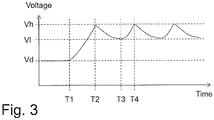
- the voltage supplied to the load 200 varies in time as will be seen in Figure 3 .
- the capacitive component 120 may further be connected to the ground wire 105.
- the capacitive component 120 may be a capacitor, such as an electrolytic capacitor at for example a couple of hundreds of ⁇ Farad,
- the electronic circuit 100 comprises a comparing unit 130, connected to the switching unit 110 and the output port 103 and arranged to obtain a value of the voltage at the output port 103.
- the comparing unit 130 is connected to the control port 111 of the switching unit 110.
- the comparing unit 130 is configured to control the switching unit 110 to be switched off when the value of the voltage exceeds a first threshold indicating a highest voltage to be fed to the output port 103; and to control the switching unit 110 to be switched on when the value of the voltage is below a second threshold indicating a least voltage to be fed to the output port 103.
- the highest voltage is related to the over-voltage against which the load is to be protected.
- the least voltage is related to a voltage required for driving the load.
- Figure 3 illustrates the voltage at the output port 103 as a function of time.
- the voltage over the load 200 is at a required driving voltage Vd.
- the load 200 operates normally.
- the voltage begins to increase, i.e. the load 200 may potentially be exposed to a harmful over-voltage.
- the load 200 is not harmed until a first voltage Vh, as an example of the highest voltage mentioned in conjunction with Figure 2 , is reached. Therefore, the comparing unit 130 makes sure that the switching unit 110 is switched off at a second time instant T2 in order to prevent the voltage from the power source 300 from reaching the load 200.
- the capacitive component 120 begins to discharge its stored energy by feeding a voltage to the load 200 until the voltage at the load 200 is at a second voltage VI, as an example of the least voltage mentioned in conjunction with Figure 2 .
- the second voltage VI is reached at a third time instant T3.
- the second voltage VI is well above the required driving voltage Vd, but at the same time the second voltage VI is not harmful to the load 200.
- the comparing unit 130 makes sure that the switching unit 110 is switched on in order to feed the voltage from the power source 300 to the load 200. Consequently, the capacitive component 120 is charged by the voltage originating from the power source 300, since when the voltage reaches the load 200, the voltages also reaches the capacitive component 120. Therefore, the voltage over the load 200 begins to increase again and at a fourth time instant T4, the switching unit 110 switches off the voltage anew.
- the voltage over the load 200 varies in this manner until, the power source 300 no longer delivers a over-voltage.
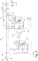
- Figure 4 shows further exemplifying embodiments of the electronic circuit 100 of Figure 2 .
- the switching unit 110 is exemplified by a transistor 410, having a gate 411, a source 412 and a drain 413.
- the transistor may be an N-channel Metal Oxide Semiconductor (N-MOS) power transistor.
- the capacitive component 120 is exemplified by a capacitor 420 of for example 1000 ⁇ F.
- the load 200 is denoted 470. Furthermore, the load 470 may have an exemplifying resistance of 50 ohms.
- the comparing unit 130 is exemplified by a set of components 430.
- a comparing entity 431 is driven by a drive voltage Vx, such as +10 V.
- the comparing entity 431, such as LM393, comprises a comparator 432 which compares the Reference voltage, such as ground, to the voltage at output port 403, being an example of the output port 103.
- the set of components 430 constituting the comparing unit 130 may also include resistors 433, 434, respectively.
- the resistors 433, 434 provides a voltage divider for suitable for input to the comparing entity 431.
- a further set of components 440 may be arranged to activate, i.e. supply power to, the components 431, 432, 433, 434 conditionally upon the voltage at an input port 401, which is an example of the input port 101.
- a comparing entity 443, such as LM393, comprises a further comparator 444.
- a transistor 446, or a further switching unit, may be a bipolar NPN-transistor. The transistor 446 is thus configured to perform the actual switching of the power supplied to the components 431 to 434. When the transistor 446 is switched off, the components 431 to 434 are inactivated.
- the further set of components 440 may be arranged and configured to supply power to the set of components 430 when the voltage at the input port 401 is at or below - 65 V. At - 65 V the exemplifying limit of - 75 V is being approached. Thus, the electronic circuit 100 must be prepared to switch off the switching unit 410 as soon as a harmful voltage may reach the load 470.
- a kind of two-step comparing unit may be said to comprise the set of components 450.
- power consumed for protecting the load 470 against over-voltage is somewhat reduced as compared to supplying power to the set of components 430 all the time.
- the electronic circuit 100 further comprises a further comparing unit, which may comprise the further set of components 440.
- the further comparing unit may include a further switching unit 446, which may be connected to the comparing entity 431. Additionally, the further comparing unit may be connected to the input port 401 and arranged to obtain a further value of the voltage at the input port 401.
- the further comparing unit may be configured to control the further switching unit 446 to be switched on when the further value exceeds a third threshold indicating that the highest voltage to be fed to the output port 403 is being approached, and to control the further switching unit 446 to be switched off when the further value is below the third threshold.
- Figure 4 also shows a further resistor 451 , which may have an exemplifying value of 1 mOhms.
- the word “arrange” relates to how the components are connected and mounted.
- the word “configure” relates to parameters of the components, e.g. for a resistor - resistance, for a transistor - voltage threshold, internal resistance etc., and so on for various components or units.
Landscapes
- Emergency Protection Circuit Devices (AREA)
- Direct Current Feeding And Distribution (AREA)
- Electronic Switches (AREA)
Claims (6)
- Elektronischer Schaltkreis (100) zum Schutz einer Last (200) vor Überspannung, umfassend:einen Eingangsanschluss (101) zum Empfangen einer Spannung von einer Leistungsquelle (300);einen Ausgangsanschluss (103) zum Zuführen der Spannung an die Last (200);eine Schalteinheit (110), angeschlossen an den Eingangsanschluss (101) und den Ausgangsanschluss (103), wobei die Schalteinheit (110) angeordnet ist, die Spannung vom Eingangsanschluss (101) ein- und auszuschalten;eine kapazitive Komponente (120), angeschlossen an den Ausgangsanschluss (103), wobei die kapazitive Komponente (120) angeordnet ist, die Spannung zu empfangen, wenn die Schalteinheit (110) eingeschaltet ist, und dem Ausgangsanschluss (103) Spannung zuzuführen, wenn die Schalteinheit (110) ausgeschaltet ist; dadurch gekennzeichnet, dass der elektronische Schaltkreis ferner umfasst:eine Vergleichseinheit (130), angeschlossen an die Schalteinheit (110) und den Ausgangsanschluss (103) und angeordnet, einen Wert der Spannung am Ausgangsanschluss (103) abzunehmen; wobei die Vergleichseinheit (130) konfiguriert ist zum:Steuern, dass die Schalteinheit (110) ausgeschaltet wird, wenn der Wert einen ersten Schwellenwert überschreitet, der angibt, dass dem Ausgangsanschluss (103) eine höchste Spannung zugeführt wird; undSteuern, dass die Schalteinheit (110) eingeschaltet wird, wenn der Wert unter einem zweiten Schwellenwert liegt, der angibt, dass dem Ausgangsanschluss (103) eine niedrigste Spannung zugeführt wird.
- Elektronischer Schaltkreis (100) nach Anspruch 1, wobei der elektronische Schaltkreis (100) ferner einen Massedraht (105) umfasst, wobei die Spannung zwischen dem Eingangsanschluss (101) und dem Massedraht (105) empfangen wird.
- Elektronischer Schaltkreis (100) nach Anspruch 1 oder 2, wobei die Schalteinheit (110) einen Steueranschluss (111) zum Empfangen eines Steuersignals zum Ein- oder Ausschalten der Schalteinheit (110) aufweist, wobei der Steueranschluss (111) an die Vergleichseinheit (130) angeschlossen ist.
- Elektronischer Schaltkreis (100) nach einem der vorhergehenden Ansprüche, wobei die kapazitive Komponente (120) ferner an den Massedraht (105) angeschlossen ist.
- Elektronischer Schaltkreis (100) nach einem der vorhergehenden Ansprüche, wobei die Schalteinheit (110) ein Transistor ist.
- Elektronischer Schaltkreis (100) nach einem der vorhergehenden Ansprüche, wobei die kapazitive Komponente (120) ein Kondensator ist.
Applications Claiming Priority (1)
| Application Number | Priority Date | Filing Date | Title |
|---|---|---|---|
| PCT/SE2012/051405 WO2014098659A1 (en) | 2012-12-17 | 2012-12-17 | Electronic circuit for protecting a load against over-voltage |
Publications (2)
| Publication Number | Publication Date |
|---|---|
| EP2932801A1 EP2932801A1 (de) | 2015-10-21 |
| EP2932801B1 true EP2932801B1 (de) | 2017-11-15 |
Family
ID=47624395
Family Applications (1)
| Application Number | Title | Priority Date | Filing Date |
|---|---|---|---|
| EP12819033.7A Not-in-force EP2932801B1 (de) | 2012-12-17 | 2012-12-17 | Elektronische schaltung zum schutz einer last vor überspannung |
Country Status (3)
| Country | Link |
|---|---|
| US (1) | US9893510B2 (de) |
| EP (1) | EP2932801B1 (de) |
| WO (1) | WO2014098659A1 (de) |
Families Citing this family (2)
| Publication number | Priority date | Publication date | Assignee | Title |
|---|---|---|---|---|
| CN107045253B (zh) * | 2017-02-22 | 2018-11-02 | 海信集团有限公司 | 激光投影设备的器件保护方法及装置 |
| KR102382253B1 (ko) * | 2018-10-30 | 2022-04-01 | 주식회사 엘지에너지솔루션 | 메인 스위치를 위한 드라이버 회로 및 그것을 포함하는 제어 장치 |
Family Cites Families (8)
| Publication number | Priority date | Publication date | Assignee | Title |
|---|---|---|---|---|
| US5773965A (en) * | 1995-10-24 | 1998-06-30 | Rohm Co., Ltd. | Switching power supply apparatus for converting a high DC voltage into a low DC voltage |
| DE59813694D1 (de) * | 1998-03-20 | 2006-10-05 | Endress & Hauser Gmbh & Co Kg | Spannungsregelschaltung |
| US7298097B2 (en) | 2005-09-13 | 2007-11-20 | On-Bright Electronics (Shanghai) Co., Ltd. | Driver system and method with multi-function protection for cold-cathode fluorescent lamp and external-electrode fluorescent lamp |
| US8335065B2 (en) * | 2007-04-30 | 2012-12-18 | Hewlett-Packard Development Company, L.P. | Overvoltage protection in a power supply |
| US8203815B2 (en) * | 2009-05-08 | 2012-06-19 | Hamilton Sundstrand Corporation | System and method to provide transient overvoltage suppression |
| DE102009023884A1 (de) | 2009-06-04 | 2011-01-27 | Osram Gesellschaft mit beschränkter Haftung | Elektronisches Vorschaltgerät und Verfahren zum Betreiben mindestens einer Entladungslampe |
| JP2011061913A (ja) * | 2009-09-07 | 2011-03-24 | Panasonic Corp | スイッチング電源装置、及びそれに用いる半導体装置 |
| US8767357B2 (en) * | 2012-06-14 | 2014-07-01 | Analog Devices, Inc. | Overvoltage protection system for power system with multiple parallel-connected switching power supplies |
-
2012
- 2012-12-17 EP EP12819033.7A patent/EP2932801B1/de not_active Not-in-force
- 2012-12-17 US US14/652,841 patent/US9893510B2/en active Active
- 2012-12-17 WO PCT/SE2012/051405 patent/WO2014098659A1/en not_active Ceased
Non-Patent Citations (1)
| Title |
|---|
| None * |
Also Published As
| Publication number | Publication date |
|---|---|
| EP2932801A1 (de) | 2015-10-21 |
| US9893510B2 (en) | 2018-02-13 |
| WO2014098659A1 (en) | 2014-06-26 |
| US20150326005A1 (en) | 2015-11-12 |
Similar Documents
| Publication | Publication Date | Title |
|---|---|---|
| KR102379554B1 (ko) | 보호 회로 | |
| US6949961B2 (en) | Power switch structure with low RDSon and low current limit | |
| EP2706639B1 (de) | Überspannungsschutzschaltung | |
| EP2712086B1 (de) | Antriebsvorrichtung für ein spannungsbetriebenes element | |
| US20150207307A1 (en) | Boost apparatus with over-current and over-voltage protection function | |
| US20200014294A1 (en) | Surge protection circuit for switched-mode power supplies | |
| EP2919344B1 (de) | Überspannungsschutzvorrichtung und verfahren | |
| US10944392B2 (en) | Switch circuit and power supply system | |
| EP1456925B1 (de) | Mit einem mosfet implementierter polaritätsschutz | |
| US9178385B2 (en) | Backup power control system | |
| EP3082239B1 (de) | Gate-treiber zum ansteurn von stromrichtern | |
| EP2849328A1 (de) | Vorrichtung und Verfahren für Hochsetzsteller mit verbesserter Toleranz gegenüber elektrischer Überbelastung (EOS) | |
| EP3038223B1 (de) | Lasttreiberschaltung | |
| CN203747400U (zh) | 一种usb电路 | |
| US8520353B2 (en) | Electronic device with surge suppression circuit | |
| EP2932801B1 (de) | Elektronische schaltung zum schutz einer last vor überspannung | |
| US10381822B2 (en) | Oring control using low voltage device for high voltage DC rack | |
| JP5750326B2 (ja) | 電子機器の保護回路 | |
| US10298008B2 (en) | DC to DC boost converter | |
| JP2016226246A (ja) | 電源保護装置 | |
| US11108226B1 (en) | Method and apparatus for reverse over current protection | |
| US9088148B2 (en) | Protection circuit for central processing unit | |
| KR20170095145A (ko) | Dc-dc 컨버터 | |
| EP4406119B1 (de) | Leistungsschalter mit normalerweise eingeschaltetem transistor | |
| KR101734215B1 (ko) | 안정성이 향상된 양방향 비절연 dc-dc 컨버터 |
Legal Events
| Date | Code | Title | Description |
|---|---|---|---|
| PUAI | Public reference made under article 153(3) epc to a published international application that has entered the european phase |
Free format text: ORIGINAL CODE: 0009012 |
|
| 17P | Request for examination filed |
Effective date: 20150602 |
|
| AK | Designated contracting states |
Kind code of ref document: A1 Designated state(s): AL AT BE BG CH CY CZ DE DK EE ES FI FR GB GR HR HU IE IS IT LI LT LU LV MC MK MT NL NO PL PT RO RS SE SI SK SM TR |
|
| AX | Request for extension of the european patent |
Extension state: BA ME |
|
| DAX | Request for extension of the european patent (deleted) | ||
| GRAP | Despatch of communication of intention to grant a patent |
Free format text: ORIGINAL CODE: EPIDOSNIGR1 |
|
| STAA | Information on the status of an ep patent application or granted ep patent |
Free format text: STATUS: GRANT OF PATENT IS INTENDED |
|
| INTG | Intention to grant announced |
Effective date: 20170612 |
|
| GRAS | Grant fee paid |
Free format text: ORIGINAL CODE: EPIDOSNIGR3 |
|
| GRAA | (expected) grant |
Free format text: ORIGINAL CODE: 0009210 |
|
| STAA | Information on the status of an ep patent application or granted ep patent |
Free format text: STATUS: THE PATENT HAS BEEN GRANTED |
|
| AK | Designated contracting states |
Kind code of ref document: B1 Designated state(s): AL AT BE BG CH CY CZ DE DK EE ES FI FR GB GR HR HU IE IS IT LI LT LU LV MC MK MT NL NO PL PT RO RS SE SI SK SM TR |
|
| REG | Reference to a national code |
Ref country code: CH Ref legal event code: EP Ref country code: GB Ref legal event code: FG4D Ref country code: AT Ref legal event code: REF Ref document number: 947484 Country of ref document: AT Kind code of ref document: T Effective date: 20171115 |
|
| REG | Reference to a national code |
Ref country code: IE Ref legal event code: FG4D |
|
| REG | Reference to a national code |
Ref country code: FR Ref legal event code: PLFP Year of fee payment: 6 |
|
| REG | Reference to a national code |
Ref country code: DE Ref legal event code: R096 Ref document number: 602012039903 Country of ref document: DE |
|
| REG | Reference to a national code |
Ref country code: NL Ref legal event code: MP Effective date: 20171115 |
|
| REG | Reference to a national code |
Ref country code: LT Ref legal event code: MG4D |
|
| REG | Reference to a national code |
Ref country code: AT Ref legal event code: MK05 Ref document number: 947484 Country of ref document: AT Kind code of ref document: T Effective date: 20171115 |
|
| PG25 | Lapsed in a contracting state [announced via postgrant information from national office to epo] |
Ref country code: FI Free format text: LAPSE BECAUSE OF FAILURE TO SUBMIT A TRANSLATION OF THE DESCRIPTION OR TO PAY THE FEE WITHIN THE PRESCRIBED TIME-LIMIT Effective date: 20171115 Ref country code: NO Free format text: LAPSE BECAUSE OF FAILURE TO SUBMIT A TRANSLATION OF THE DESCRIPTION OR TO PAY THE FEE WITHIN THE PRESCRIBED TIME-LIMIT Effective date: 20180215 Ref country code: NL Free format text: LAPSE BECAUSE OF FAILURE TO SUBMIT A TRANSLATION OF THE DESCRIPTION OR TO PAY THE FEE WITHIN THE PRESCRIBED TIME-LIMIT Effective date: 20171115 Ref country code: ES Free format text: LAPSE BECAUSE OF FAILURE TO SUBMIT A TRANSLATION OF THE DESCRIPTION OR TO PAY THE FEE WITHIN THE PRESCRIBED TIME-LIMIT Effective date: 20171115 Ref country code: SE Free format text: LAPSE BECAUSE OF FAILURE TO SUBMIT A TRANSLATION OF THE DESCRIPTION OR TO PAY THE FEE WITHIN THE PRESCRIBED TIME-LIMIT Effective date: 20171115 Ref country code: LT Free format text: LAPSE BECAUSE OF FAILURE TO SUBMIT A TRANSLATION OF THE DESCRIPTION OR TO PAY THE FEE WITHIN THE PRESCRIBED TIME-LIMIT Effective date: 20171115 |
|
| PG25 | Lapsed in a contracting state [announced via postgrant information from national office to epo] |
Ref country code: BG Free format text: LAPSE BECAUSE OF FAILURE TO SUBMIT A TRANSLATION OF THE DESCRIPTION OR TO PAY THE FEE WITHIN THE PRESCRIBED TIME-LIMIT Effective date: 20180215 Ref country code: HR Free format text: LAPSE BECAUSE OF FAILURE TO SUBMIT A TRANSLATION OF THE DESCRIPTION OR TO PAY THE FEE WITHIN THE PRESCRIBED TIME-LIMIT Effective date: 20171115 Ref country code: LV Free format text: LAPSE BECAUSE OF FAILURE TO SUBMIT A TRANSLATION OF THE DESCRIPTION OR TO PAY THE FEE WITHIN THE PRESCRIBED TIME-LIMIT Effective date: 20171115 Ref country code: RS Free format text: LAPSE BECAUSE OF FAILURE TO SUBMIT A TRANSLATION OF THE DESCRIPTION OR TO PAY THE FEE WITHIN THE PRESCRIBED TIME-LIMIT Effective date: 20171115 Ref country code: GR Free format text: LAPSE BECAUSE OF FAILURE TO SUBMIT A TRANSLATION OF THE DESCRIPTION OR TO PAY THE FEE WITHIN THE PRESCRIBED TIME-LIMIT Effective date: 20180216 Ref country code: AT Free format text: LAPSE BECAUSE OF FAILURE TO SUBMIT A TRANSLATION OF THE DESCRIPTION OR TO PAY THE FEE WITHIN THE PRESCRIBED TIME-LIMIT Effective date: 20171115 |
|
| PG25 | Lapsed in a contracting state [announced via postgrant information from national office to epo] |
Ref country code: DK Free format text: LAPSE BECAUSE OF FAILURE TO SUBMIT A TRANSLATION OF THE DESCRIPTION OR TO PAY THE FEE WITHIN THE PRESCRIBED TIME-LIMIT Effective date: 20171115 Ref country code: CY Free format text: LAPSE BECAUSE OF FAILURE TO SUBMIT A TRANSLATION OF THE DESCRIPTION OR TO PAY THE FEE WITHIN THE PRESCRIBED TIME-LIMIT Effective date: 20171115 Ref country code: EE Free format text: LAPSE BECAUSE OF FAILURE TO SUBMIT A TRANSLATION OF THE DESCRIPTION OR TO PAY THE FEE WITHIN THE PRESCRIBED TIME-LIMIT Effective date: 20171115 Ref country code: CZ Free format text: LAPSE BECAUSE OF FAILURE TO SUBMIT A TRANSLATION OF THE DESCRIPTION OR TO PAY THE FEE WITHIN THE PRESCRIBED TIME-LIMIT Effective date: 20171115 Ref country code: SK Free format text: LAPSE BECAUSE OF FAILURE TO SUBMIT A TRANSLATION OF THE DESCRIPTION OR TO PAY THE FEE WITHIN THE PRESCRIBED TIME-LIMIT Effective date: 20171115 |
|
| REG | Reference to a national code |
Ref country code: CH Ref legal event code: PL |
|
| REG | Reference to a national code |
Ref country code: DE Ref legal event code: R097 Ref document number: 602012039903 Country of ref document: DE |
|
| PG25 | Lapsed in a contracting state [announced via postgrant information from national office to epo] |
Ref country code: PL Free format text: LAPSE BECAUSE OF FAILURE TO SUBMIT A TRANSLATION OF THE DESCRIPTION OR TO PAY THE FEE WITHIN THE PRESCRIBED TIME-LIMIT Effective date: 20171115 Ref country code: RO Free format text: LAPSE BECAUSE OF FAILURE TO SUBMIT A TRANSLATION OF THE DESCRIPTION OR TO PAY THE FEE WITHIN THE PRESCRIBED TIME-LIMIT Effective date: 20171115 Ref country code: IT Free format text: LAPSE BECAUSE OF FAILURE TO SUBMIT A TRANSLATION OF THE DESCRIPTION OR TO PAY THE FEE WITHIN THE PRESCRIBED TIME-LIMIT Effective date: 20171115 Ref country code: SM Free format text: LAPSE BECAUSE OF FAILURE TO SUBMIT A TRANSLATION OF THE DESCRIPTION OR TO PAY THE FEE WITHIN THE PRESCRIBED TIME-LIMIT Effective date: 20171115 |
|
| REG | Reference to a national code |
Ref country code: IE Ref legal event code: MM4A |
|
| PLBE | No opposition filed within time limit |
Free format text: ORIGINAL CODE: 0009261 |
|
| STAA | Information on the status of an ep patent application or granted ep patent |
Free format text: STATUS: NO OPPOSITION FILED WITHIN TIME LIMIT |
|
| PG25 | Lapsed in a contracting state [announced via postgrant information from national office to epo] |
Ref country code: MT Free format text: LAPSE BECAUSE OF NON-PAYMENT OF DUE FEES Effective date: 20171217 Ref country code: LU Free format text: LAPSE BECAUSE OF NON-PAYMENT OF DUE FEES Effective date: 20171217 |
|
| REG | Reference to a national code |
Ref country code: BE Ref legal event code: MM Effective date: 20171231 |
|
| 26N | No opposition filed |
Effective date: 20180817 |
|
| PG25 | Lapsed in a contracting state [announced via postgrant information from national office to epo] |
Ref country code: IE Free format text: LAPSE BECAUSE OF NON-PAYMENT OF DUE FEES Effective date: 20171217 |
|
| PG25 | Lapsed in a contracting state [announced via postgrant information from national office to epo] |
Ref country code: CH Free format text: LAPSE BECAUSE OF NON-PAYMENT OF DUE FEES Effective date: 20171231 Ref country code: BE Free format text: LAPSE BECAUSE OF NON-PAYMENT OF DUE FEES Effective date: 20171231 Ref country code: LI Free format text: LAPSE BECAUSE OF NON-PAYMENT OF DUE FEES Effective date: 20171231 Ref country code: SI Free format text: LAPSE BECAUSE OF FAILURE TO SUBMIT A TRANSLATION OF THE DESCRIPTION OR TO PAY THE FEE WITHIN THE PRESCRIBED TIME-LIMIT Effective date: 20171115 |
|
| PG25 | Lapsed in a contracting state [announced via postgrant information from national office to epo] |
Ref country code: HU Free format text: LAPSE BECAUSE OF FAILURE TO SUBMIT A TRANSLATION OF THE DESCRIPTION OR TO PAY THE FEE WITHIN THE PRESCRIBED TIME-LIMIT; INVALID AB INITIO Effective date: 20121217 Ref country code: MC Free format text: LAPSE BECAUSE OF FAILURE TO SUBMIT A TRANSLATION OF THE DESCRIPTION OR TO PAY THE FEE WITHIN THE PRESCRIBED TIME-LIMIT Effective date: 20171115 |
|
| PG25 | Lapsed in a contracting state [announced via postgrant information from national office to epo] |
Ref country code: MK Free format text: LAPSE BECAUSE OF FAILURE TO SUBMIT A TRANSLATION OF THE DESCRIPTION OR TO PAY THE FEE WITHIN THE PRESCRIBED TIME-LIMIT Effective date: 20171115 |
|
| PG25 | Lapsed in a contracting state [announced via postgrant information from national office to epo] |
Ref country code: TR Free format text: LAPSE BECAUSE OF FAILURE TO SUBMIT A TRANSLATION OF THE DESCRIPTION OR TO PAY THE FEE WITHIN THE PRESCRIBED TIME-LIMIT Effective date: 20171115 |
|
| PG25 | Lapsed in a contracting state [announced via postgrant information from national office to epo] |
Ref country code: PT Free format text: LAPSE BECAUSE OF FAILURE TO SUBMIT A TRANSLATION OF THE DESCRIPTION OR TO PAY THE FEE WITHIN THE PRESCRIBED TIME-LIMIT Effective date: 20171115 |
|
| PG25 | Lapsed in a contracting state [announced via postgrant information from national office to epo] |
Ref country code: AL Free format text: LAPSE BECAUSE OF FAILURE TO SUBMIT A TRANSLATION OF THE DESCRIPTION OR TO PAY THE FEE WITHIN THE PRESCRIBED TIME-LIMIT Effective date: 20171115 Ref country code: IS Free format text: LAPSE BECAUSE OF FAILURE TO SUBMIT A TRANSLATION OF THE DESCRIPTION OR TO PAY THE FEE WITHIN THE PRESCRIBED TIME-LIMIT Effective date: 20180315 |
|
| PGFP | Annual fee paid to national office [announced via postgrant information from national office to epo] |
Ref country code: GB Payment date: 20221227 Year of fee payment: 11 Ref country code: FR Payment date: 20221227 Year of fee payment: 11 |
|
| PGFP | Annual fee paid to national office [announced via postgrant information from national office to epo] |
Ref country code: DE Payment date: 20221228 Year of fee payment: 11 |
|
| REG | Reference to a national code |
Ref country code: DE Ref legal event code: R119 Ref document number: 602012039903 Country of ref document: DE |
|
| GBPC | Gb: european patent ceased through non-payment of renewal fee |
Effective date: 20231217 |
|
| PG25 | Lapsed in a contracting state [announced via postgrant information from national office to epo] |
Ref country code: DE Free format text: LAPSE BECAUSE OF NON-PAYMENT OF DUE FEES Effective date: 20240702 |
|
| PG25 | Lapsed in a contracting state [announced via postgrant information from national office to epo] |
Ref country code: GB Free format text: LAPSE BECAUSE OF NON-PAYMENT OF DUE FEES Effective date: 20231217 |
|
| PG25 | Lapsed in a contracting state [announced via postgrant information from national office to epo] |
Ref country code: FR Free format text: LAPSE BECAUSE OF NON-PAYMENT OF DUE FEES Effective date: 20231231 |
|
| PG25 | Lapsed in a contracting state [announced via postgrant information from national office to epo] |
Ref country code: GB Free format text: LAPSE BECAUSE OF NON-PAYMENT OF DUE FEES Effective date: 20231217 Ref country code: FR Free format text: LAPSE BECAUSE OF NON-PAYMENT OF DUE FEES Effective date: 20231231 Ref country code: DE Free format text: LAPSE BECAUSE OF NON-PAYMENT OF DUE FEES Effective date: 20240702 |