EP3534292A1 - Optical module and processing method therefor, and terminal device - Google Patents
Optical module and processing method therefor, and terminal device Download PDFInfo
- Publication number
- EP3534292A1 EP3534292A1 EP17931166.7A EP17931166A EP3534292A1 EP 3534292 A1 EP3534292 A1 EP 3534292A1 EP 17931166 A EP17931166 A EP 17931166A EP 3534292 A1 EP3534292 A1 EP 3534292A1
- Authority
- EP
- European Patent Office
- Prior art keywords
- optical sensor
- sensor
- air gap
- optical
- substrate
- Prior art date
- Legal status (The legal status is an assumption and is not a legal conclusion. Google has not performed a legal analysis and makes no representation as to the accuracy of the status listed.)
- Withdrawn
Links
Images



Classifications
-
- G—PHYSICS
- G06—COMPUTING OR CALCULATING; COUNTING
- G06V—IMAGE OR VIDEO RECOGNITION OR UNDERSTANDING
- G06V40/00—Recognition of biometric, human-related or animal-related patterns in image or video data
- G06V40/10—Human or animal bodies, e.g. vehicle occupants or pedestrians; Body parts, e.g. hands
- G06V40/12—Fingerprints or palmprints
- G06V40/13—Sensors therefor
- G06V40/1318—Sensors therefor using electro-optical elements or layers, e.g. electroluminescent sensing
-
- G—PHYSICS
- G06—COMPUTING OR CALCULATING; COUNTING
- G06V—IMAGE OR VIDEO RECOGNITION OR UNDERSTANDING
- G06V40/00—Recognition of biometric, human-related or animal-related patterns in image or video data
- G06V40/10—Human or animal bodies, e.g. vehicle occupants or pedestrians; Body parts, e.g. hands
- G06V40/12—Fingerprints or palmprints
-
- G—PHYSICS
- G06—COMPUTING OR CALCULATING; COUNTING
- G06V—IMAGE OR VIDEO RECOGNITION OR UNDERSTANDING
- G06V10/00—Arrangements for image or video recognition or understanding
- G06V10/10—Image acquisition
- G06V10/12—Details of acquisition arrangements; Constructional details thereof
- G06V10/14—Optical characteristics of the device performing the acquisition or on the illumination arrangements
- G06V10/147—Details of sensors, e.g. sensor lenses
-
- H—ELECTRICITY
- H04—ELECTRIC COMMUNICATION TECHNIQUE
- H04M—TELEPHONIC COMMUNICATION
- H04M1/00—Substation equipment, e.g. for use by subscribers
-
- H—ELECTRICITY
- H10—SEMICONDUCTOR DEVICES; ELECTRIC SOLID-STATE DEVICES NOT OTHERWISE PROVIDED FOR
- H10F—INORGANIC SEMICONDUCTOR DEVICES SENSITIVE TO INFRARED RADIATION, LIGHT, ELECTROMAGNETIC RADIATION OF SHORTER WAVELENGTH OR CORPUSCULAR RADIATION
- H10F39/00—Integrated devices, or assemblies of multiple devices, comprising at least one element covered by group H10F30/00, e.g. radiation detectors comprising photodiode arrays
- H10F39/011—Manufacture or treatment of image sensors covered by group H10F39/12
-
- H—ELECTRICITY
- H10—SEMICONDUCTOR DEVICES; ELECTRIC SOLID-STATE DEVICES NOT OTHERWISE PROVIDED FOR
- H10F—INORGANIC SEMICONDUCTOR DEVICES SENSITIVE TO INFRARED RADIATION, LIGHT, ELECTROMAGNETIC RADIATION OF SHORTER WAVELENGTH OR CORPUSCULAR RADIATION
- H10F39/00—Integrated devices, or assemblies of multiple devices, comprising at least one element covered by group H10F30/00, e.g. radiation detectors comprising photodiode arrays
- H10F39/80—Constructional details of image sensors
- H10F39/804—Containers or encapsulations
-
- H—ELECTRICITY
- H10—SEMICONDUCTOR DEVICES; ELECTRIC SOLID-STATE DEVICES NOT OTHERWISE PROVIDED FOR
- H10F—INORGANIC SEMICONDUCTOR DEVICES SENSITIVE TO INFRARED RADIATION, LIGHT, ELECTROMAGNETIC RADIATION OF SHORTER WAVELENGTH OR CORPUSCULAR RADIATION
- H10F39/00—Integrated devices, or assemblies of multiple devices, comprising at least one element covered by group H10F30/00, e.g. radiation detectors comprising photodiode arrays
- H10F39/80—Constructional details of image sensors
- H10F39/806—Optical elements or arrangements associated with the image sensors
-
- H—ELECTRICITY
- H10—SEMICONDUCTOR DEVICES; ELECTRIC SOLID-STATE DEVICES NOT OTHERWISE PROVIDED FOR
- H10F—INORGANIC SEMICONDUCTOR DEVICES SENSITIVE TO INFRARED RADIATION, LIGHT, ELECTROMAGNETIC RADIATION OF SHORTER WAVELENGTH OR CORPUSCULAR RADIATION
- H10F39/00—Integrated devices, or assemblies of multiple devices, comprising at least one element covered by group H10F30/00, e.g. radiation detectors comprising photodiode arrays
- H10F39/80—Constructional details of image sensors
- H10F39/806—Optical elements or arrangements associated with the image sensors
- H10F39/8063—Microlenses
-
- H—ELECTRICITY
- H10—SEMICONDUCTOR DEVICES; ELECTRIC SOLID-STATE DEVICES NOT OTHERWISE PROVIDED FOR
- H10F—INORGANIC SEMICONDUCTOR DEVICES SENSITIVE TO INFRARED RADIATION, LIGHT, ELECTROMAGNETIC RADIATION OF SHORTER WAVELENGTH OR CORPUSCULAR RADIATION
- H10F39/00—Integrated devices, or assemblies of multiple devices, comprising at least one element covered by group H10F30/00, e.g. radiation detectors comprising photodiode arrays
- H10F39/80—Constructional details of image sensors
- H10F39/811—Interconnections
-
- H—ELECTRICITY
- H10—SEMICONDUCTOR DEVICES; ELECTRIC SOLID-STATE DEVICES NOT OTHERWISE PROVIDED FOR
- H10F—INORGANIC SEMICONDUCTOR DEVICES SENSITIVE TO INFRARED RADIATION, LIGHT, ELECTROMAGNETIC RADIATION OF SHORTER WAVELENGTH OR CORPUSCULAR RADIATION
- H10F77/00—Constructional details of devices covered by this subclass
- H10F77/50—Encapsulations or containers
-
- H—ELECTRICITY
- H10—SEMICONDUCTOR DEVICES; ELECTRIC SOLID-STATE DEVICES NOT OTHERWISE PROVIDED FOR
- H10W—GENERIC PACKAGES, INTERCONNECTIONS, CONNECTORS OR OTHER CONSTRUCTIONAL DETAILS OF DEVICES COVERED BY CLASS H10
- H10W70/00—Package substrates; Interposers; Redistribution layers [RDL]
- H10W70/60—Insulating or insulated package substrates; Interposers; Redistribution layers
-
- H—ELECTRICITY
- H10—SEMICONDUCTOR DEVICES; ELECTRIC SOLID-STATE DEVICES NOT OTHERWISE PROVIDED FOR
- H10W—GENERIC PACKAGES, INTERCONNECTIONS, CONNECTORS OR OTHER CONSTRUCTIONAL DETAILS OF DEVICES COVERED BY CLASS H10
- H10W72/00—Interconnections or connectors in packages
- H10W72/851—Dispositions of multiple connectors or interconnections
- H10W72/874—On different surfaces
- H10W72/884—Die-attach connectors and bond wires
Definitions
- Embodiments of the present application relate to the technical field of optical devices, and in particular, relate to an optical module, a fabrication method thereof, and a terminal device using the same.
- the mobile terminals are being extensively applied in people's daily life and work.
- the mobile terminals are all equipped with a fingerprint identification apparatus, which performs various operations such as unlocking based fingerprint identification, and password setting and the like.
- a fingerprint identification apparatus which performs various operations such as unlocking based fingerprint identification, and password setting and the like.
- capacitive fingerprint apparatuses and optical fingerprint identification apparatuses are two types of commonly used fingerprint identification apparatuses.
- the conventional capacitive fingerprint identification apparatus has a limited penetration capability, a complicated ID structure, a great module thickness, a limited placement position, and thus are unfavorable to lightening and thinning and miniaturization of the mobile terminals.
- the current optical fingerprint identification apparatus has a strong penetration capability and supports random placement below the screen.
- the optical fingerprint identification apparatus when the optical fingerprint identification apparatus is arranged below the screen of a terminal, the optical fingerprint identification apparatus needs to be superimposed over the battery of the mobile terminal, and many parts or components in the packaging structure of the optical fingerprint identification apparatus are superimposed; and in another aspect, based on the requirement on identification precision, the higher the precision, the thicker the apparatus, which is also unfavorable to lightening and thinning and miniaturization of the mobile terminal.
- embodiments of the present application provides an optical module, a fabrication method thereof, and a terminal using the same, to solve the problem that the optical module in the related art has a greater thickness which is unfavorable to lightening and thinning and miniaturization of a mobile terminal.
- an optical module includes a lens and a sensor package.
- the lens is positioned at an uppermost position of the optical module and attached to a lower position of a terminal screen, and is configured to transmit light passing through the screen;
- the sensor package includes an optical sensor, where a photosensitive region is arranged on an upper surface of the optical sensor, and the photosensitive region is configured to receive light passing through the lens; and the sensor package further includes an air gap, and the photosensitive region of the optical sensor is configured to receive the light passing through the screen via the air gap.
- the optical module includes a lens and a sensor package.
- the lens is positioned at an uppermost position of the optical module and attached to a lower position of a terminal screen, and is configured to transmit light passing through the screen;
- the sensor package includes an optical sensor, where a photosensitive region is arranged on an upper surface of the optical sensor, and the photosensitive region is configured to receive light passing through the lens; and an air gap is defined between the lens and the sensor package, and the photosensitive region of the optical sensor is configured to receive the light passing through the screen via the air gap.
- an optical module fabrication method includes: packaging an optical sensor to form a sensor package having an air gap, where a photosensitive region configured to receive light is arranged on an upper surface of the optical sensor, and the air gap in the sensor package is positioned above the photosensitive region of the optical sensor; and forming an optical module by using the sensor package and a lens configured to transmit light, where the lens is positioned at an uppermost position of the optical module.
- another optical module fabrication method includes: packaging an optical sensor to form a sensor package, where a photosensitive region configured to receive light is arranged on an upper surface of the optical sensor; defining an air gap below a lens configured to transmit light; and forming an optical module using the sensor package and the lens having the air gap, where the lens is positioned at an uppermost position of the optical module, and the photosensitive region of the optical sensor is configured to receive light via the air gap.
- a terminal device includes the above described optical module.
- the air gap is arranged in the senor package in which the optical sensor is packaged, and the optical sensor receives light passing through the screen via the air gap, and thus practices imaging.
- the air gap may be filled with a corresponding gaseous medium.
- the gaseous medium has a low refractive index, and thus may effectively reducing interference to the light for imaging reaching the optical sensor.
- accuracy of fingerprint detection and identification is ensured.
- the accuracy of detection and identification is higher. From another perspective, the same accuracy is achieved with a smaller thickness, such that a balancing effect is achieved between accuracy and thickness of the optical module, and the optical module becomes thinner while the accuracy of detection and identification is maintained.
- Reference numerals and denotations thereof 10-lens; 11-parallel light channel; 21-optical sensor; 211-photosensitive region; 212-metal pad; 22-air gap; 23-substrate; 231-discrete device; 232-tin ball; 233-pad; 24-plastic packaging adhesive; 25-lid; 26-carrier; 27-interposer; 30-filter layer; 60-screen; 81-first die attach film; 82-second die attach film; 83-third die attach film; 84-fourth die attach film; 90-bond wire; 91-wire; 92-bump; and 93-redistribution layer.
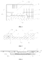
- an optical module includes a lens 10 and a sensor package.
- the lens 10 is positioned at an uppermost position of the optical module and attached to a lower position of a terminal screen 60, and is configured to transmit light passing through the screen 60;
- the sensor package includes an optical sensor 21, where a photosensitive region 211 is arranged on an upper surface of the optical sensor 21, and the photosensitive region 211 is configured to receive light passing through the lens 10; and the sensor package further includes an air gap 22, and the photosensitive region 211 of the optical sensor 21 is configured to receive the light passing through the screen 60 via the air gap 22.
- the optical sensor 21 in the optical module is configured to receive light for use in imaging, and hence generate an image based on the light.
- the air gap 22 is arranged in the sensor package including the optical sensor; and the optical sensor is configured to receive light passing through the screen via the air gap, and hence achieve imaging.
- the air gap 22 may be filled with a corresponding gaseous medium.
- the gaseous medium has a low refractive index, and thus may effectively reducing interference to the light for imaging reaching the optical sensor. In this way, accuracy of fingerprint detection and identification is ensured.
- the accuracy of detection and identification is higher. From another perspective, the same accuracy is achieved with a smaller thickness, such that a balancing effect is achieved between accuracy and thickness of the optical module, and the optical module becomes thinner while the accuracy of detection and identification is maintained.
- the optical module having the air gap 22 according to this embodiment has an even smaller thickness.
- an object distance between the optical sensor 21 and a subject under detection may be increased.
- the optical module according to this embodiment may reduce moire in the detection process, and improve the identification accuracy.
- the air gap 22 may be an air interlayer, or may be replaced by a transparent superimposed substance; and in the packaging process, the air gap 22 may be practiced by a suitable packaging process, as long as the air gap 22 is defined between the lens 10 and the optical sensor 21.
- the air gap 22 may have a thickness in the range of 200 to 500 ⁇ m, which may improve fingerprint identification performance.
- the sensor package includes a substrate 23.
- the substrate 23 may be arranged at different positions of the sensor package.
- the substrate 23 is arranged at a lowermost position of the sensor package, and the optical sensor 21 is positioned on an upper surface of the substrate 23.
- the substrate 23 may be positioned above the optical sensor 21.
- the substrate 23 is configured to mount and bear other structures of the sensor package.
- the substrate 23 is configured to mount the optical sensor 21, and practice electrical connection between the optical sensor 21 and the substrate 23, such that a signal of the optical sensor 23 is output outside the sensor package via the substrate 23.
- the substrate 23 may be practiced by a combination of a rigid board and a flexible board.
- the surface mount technology (SMT) and reinforced flexible printed circuit (FPC) achieve an even smaller thickness, and thus the thickness of the substrate 23 maybe further reduced.
- the substrate 23 employing the combination of the rigid board and the flexible board may have an entire thickness less than or equal to 1 mm.
- a circuit configured to transmit the signal of the optical sensor 21 may be embedded on the substrate 23.
- the substrate 23 may be provided with a discrete device 231 or may be provided with no discrete device 231.
- the discrete device 231 includes, for example, a resistor for protecting circuit, or a capacitor for storing energy, or the like. Nevertheless, the discrete device 231 may be arranged according to the actual needs.
- the substrate 23 may be connected to other structures via a connection wire 91 (as illustrated in FIG. 1 ) or the like, and thus practice transfer of signals, power and the like.
- the substrate 23 may also connected to other external structures of the sensor package via a pad or a tin ball 232 or the like, and thus practice transfer of signals, power and the like.
- the optical sensor 21 may be a complementary metal oxide semiconductor (CMOS) sensor.
- CMOS complementary metal oxide semiconductor
- the CMOS sensor includes a photosensitive region 211 for photosensitive imaging.
- the optical sensor 21 may be integrated with a logic circuit and an optical sensor, and have a function of converting a received optical signal to an electrical signal. By packaging and fabrication, the optical sensor 21 may lead an electrical signal on the sensor to the exterior of the package, for ease of connection to an external device.
- the optical sensor 21 may be bonded to the upper surface of the substrate 23 via a fourth die attach film 84.
- the fourth die attach film 84 below the optical sensor 21 may have a thickness greater than or equal to 1 ⁇ m, and thus may absorb light having a specific wavelength. According to different product requirements, a wavelength range may be determined, and thus a material of the fourth die attach film accommodating the requirements may be selected.
- the optical sensor 21 may be connected to the substrate 23 in a wirebond fashion.
- a metal pad 212 of the optical sensor 21 may be connected to a pad 233 on the substrate 23.
- This connection may involve physical connection or may involve connections of both signals and power.
- the wirebond fashion achieves a better performance relative to a chip scale package (CSP) fashion, and in this fashion, spherical image interference may not easily occur.
- the optical sensor 21 may also be electrically connected to the substrate 23 by bump mounting.
- the optical sensor 21 is connected to the substrate 23 by a bond wire 90 of the optical module.
- the bond wire 90 is configured to transfer an electrical signal from the optical sensor 21 to the substrate 23, and a protective die attach film coated outside is arranged on the exterior of the bond wire 90.
- the protective adhesive layer coating the bond wire 90 may have such characteristics of low shrinkage rate, water-proofing and the like, and thus may better protect the bond wire 90 from environmental impacts.
- the function of the protective adhesive layer is not limited to such protection.
- the bond wire 90 may be a gold wire and/or a copper wire.
- a specific material of the bond wire 90 may be determined according to the actual needs, cost and the like factors. For example, when a plurality of bond wires 90 are needed, some may be gold wires and some may be copper wires; or all the bond wires 90 may be fabricated from the same material, both the gold wires or the copper wires or the like, which is not specifically defined herein.
- the sensor package further includes a plastic packaging adhesive 24 configured to package and protect the optical sensor 21 and the like structures.
- the plastic packaging adhesive 24 defines a support structure surrounding outside the optical sensor 21, the plastic packaging adhesive 24 is arranged on the upper surface of the substrate 23, and an upper surface of the plastic packaging adhesive 24 is above the upper surface of the optical sensor 21, such that the air gap 22 is defined between the plastic packaging adhesive 24 and the optical sensor 21.
- an opening at least exposing from the photosensitive region 211 is defined at a portion of the plastic packaging adhesive 24 that is above the optical sensor 21, such that the air gap 22 is defined between the plastic packaging adhesive 24 and the optical sensor 23.
- a top of the plastic packaging adhesive 24 is connected to the screen 60 via a second die attach film 82, such that the air gap 22 is defined above the optical sensor 21.
- the plastic packaging adhesive 24 is a light shielding material.
- the plastic packaging adhesive 24 may be in a dark color to achieve the effect of shielding light.
- the plastic packaging adhesive 24 may also be other materials that are capable of absorbing light having a specific wavelength, which is not limited herein.
- the support structure formed by the plastic packaging adhesive 24 may have a thickness that may be adjusted according to the actual needs, as long as the air gap 22 is defined and has a height accommodating the requirement.
- the thickness of the air gap 22 is greater than or equal to 10 ⁇ m.
- the air gap may be flexibly adjusted based on the thickness of the support structure, as compared with the fabrication processes of the optical module such as a mold process (injection molding and the like fabrication processes), the fashion of forming the support structure by the plastic packaging adhesive 24 makes a more flexible adjustment of the thickness of the optical module and a lower practice cost.
- the lens 10 is bonded to a lower position of the screen 60 via a first die attach film 81, the lens 10 corresponds to the optical sensor 21, and the air gap 22 is positioned below the lens 10 and above the optical sensor 21.
- the screen 60 may be an organic light-emitting diode (OLED) material, but is not limited to such material.
- OLED organic light-emitting diode
- the screen 60 may have a foam/black adhesive layer on a rear side thereof.
- the foam or black adhesive layer is attached on a side of the screen 60 proximal to a metal cathode or on the metal cathode, to prevent light leakage in some occasions, and a region corresponding to the lens 10 on the screen 60 is a light transmission region for light to pass through.
- the second die attach film 82 is further configured to bond the plastic packaging adhesive 24 to the screen 60.
- the plastic packaging adhesive 24 may be bonded to a structure such as the foam or black adhesive layer or the like equipped on the screen via the second die attach film 82.
- the second die attach film 82 may be a material having the effect of absorbing light having a specific wavelength to prevent ambient light from passing through the second die attach film 82 to cause light leakage. In this way, light leakage is prevented and impacts on the identification accuracy of the optical sensor 21 are eliminated.
- the lens 10 may absorb light having a specific wavelength, such that the lens achieves a filtering effect. However, the lens 10 is not limited to such effect.
- the lens 10 may also be provided with an optical modulation opening or channel.
- the optical modulation opening has an effect similar to a pinhole in pinhole imaging.
- the channel allows the light to pass through to form a collimated light, and obliquely incident light may collide with a wall of the channel when passing through the lens 10 and thus may be absorbed, such that the light passing through the lens 10 is a direct light.
- the first die attach film 81 for bonding the lens 10 may be fabricated by a material that is capable of transmitting light having a specific wavelength, such that the light transmission is ensured while the lens 10 is bonded. In this way, detection and identification of the optical module may not be affected.
- the lens 10 is a light path modulation device, and practices transmission of special light by modulating a light path.
- the lens 10 is configured to improve the fingerprint identification performance, and may be arranged below the screen 60 or above the optical sensor 21.
- the lens 10 may be integrated in the package by packaging, or may be added during subsequent assembling of the module.
- the lens 10 needs to cover the photosensitive region of the optical sensor 21.
- the optical module includes a filter layer 30, the lens 10 may be arranged above the filter layer 30 or arranged below the filter layer 30.
- the first die attach film 81 has a thickness less than or equal to 200 ⁇ m.
- the sensor package further includes a lid 25.
- the lid 25 is positioned on the upper surface of the plastic packaging adhesive 24, and the air gap 22 is defined between the lid 25 and the optical sensor 21.
- the lid 25 is a lid provided with an opening, and the opening on the lid 25 corresponds to the photosensitive region 211 of the optical sensor 21, such that the air gap is defined between the lid 25 and the optical sensor 21.
- the substrate 23 is provided with an opening, the optical sensor 21 is positioned in the opening on the substrate 23, the upper surface of the substrate 23 is above the upper surface of the optical sensor 21, and the air gap 22 is defined between the substrate 23 and the optical sensor 21.
- the substrate 23 may be replaced by a carrier 26.
- the sensor package further includes the carrier 26, where the carrier 26 is positioned at a lowermost position of the sensor package.
- a side surface of the carrier 26 coats the optical sensor 21, which increases an area of the package besides the optical sensor 21, and achieves effects of expanding a fan-out redistribution region and protecting the chip.
- the carrier 26 may be a silicon sheet, a plastic packaging material or a substrate.
- a groove for receiving the optical sensor 21 may be formed by a trenching process, or the optical sensor 21 may be coated by an open mold process.
- a structure having effects of bearing and protecting the optical sensor 21 similar to the carrier 26 may be formed by coating the optical sensor 21 with the plastic packaging adhesive 24.
- the carrier 26 may also be fabricated from other materials by other fabrication processes. Using fabrication of the carrier 26 using the plastic packaging adhesive 24 as an example, the optical sensor 21 is positioned on the upper surface of the plastic packaging adhesive 24, and an upper surface of the carrier 26 (that is, the plastic packaging adhesive 24) is flush with the upper surface of the optical sensor 21.
- the carrier 26 is provided with an opening, the optical sensor 21 is positioned in the opening on the carrier 26, and an upper surface of the carrier 26 is flush with the upper surface of the optical sensor 21.
- An interposer 27 or a lid 25 is arranged over the plastic packaging adhesive 24 or the carrier 26, where the air gap 22 is defined between the interposer 27 or the lid 25 and the optical sensor 21.
- the interposer 27 or the lid 25 is a structure having an opening, and the air gap 22 may be defined between the opening of the interposer 27 or the lid 25 and the optical sensor 21.
- the optical module further includes a filter layer 30, where the filter layer 30 is positioned between the lens 10 and the optical sensor 21.
- the filter layer 30 may be a filter sheet.
- the filter sheet has an effect of absorbing light having a specific wavelength, and may filter light according to the actual needs.
- the filter sheet is equivalent to a bandpass filter sheet.
- the filter layer 30 may at least filter a portion of the light, such that undesired light is prevented from causing interference and impacts on the detection and identification of the optical sensor 21. For example, during fingerprint identification, if a user places his or her finger randomly, a portion of ambient light may be transmitted to the optical module. If the ambient light, together with light reflected by the finger, reaches the optical sensor 21 at the same time, identification by the optical sensor 21 may be inaccurate or may fail. In this case, the undesired light generated by the ambient light needs to be removed, such that accuracy of the identification is not affected.
- a lower part of the filter layer 30 is bonded to the optical sensor 21 via a third die attach film 83 (as illustrated in FIG. 1 ) which is capable of transmitting light having a wavelength in a specific range.
- the specific range may be specifically determined according to different product requirements.
- the filter layer 30 is a filter sheet, at least one surface of the filter sheet may be provided with a reflective plating layer which may reflect light having some wavelengths, such that the undesired light is prevented from passing through.
- the light to be filtered herein is light which adversely affects the accuracy of identification.
- Upper and lower surfaces of the filter sheet may be both provided with a reflective plating layer, or either of the upper and lower surfaces of the filter sheet may be provided with a reflective plating layer, or neither of the upper and lower surfaces of the filter sheet is provided with a reflective plating layer.
- the filter layer 30 covers the photosensitive region 211 of the optical sensor 21, and is arranged under the lens 10.
- An area of the filter layer 30 is greater than or equal to the area of the photosensitive region 211 of the optical sensor 21, and the area of the lens is greater than or equal to the area of the filter layer 30. In this way, it may be ensured that the light reaching the filter layer 30 is processed by the lens 10 (for example, focusing processing).
- the area of the filter layer 30 is greater than or equal to the area of the photosensitive region 211 of the optical sensor 21, and the filter layer 30 covers the photosensitive region 211 of the optical sensor 21, such that the light reaching the photosensitive region 211 of the optical sensor 21 is processed by the filter layer 30 to ensure the accuracy of detection and identification of the optical module.
- the filter layer 30 may employ a transparent or semi-transparent material as a base material, and achieve an effect of cutting of light in a specific waveband by coating on the surface of the filter layer 30.
- the filter layer 30 is arranged above the optical sensor 21.
- the filter layer 30 may employ the optical sensor 21 as a base material, and achieve an effect of filtering light by directly coating on the surface of optical sensor 21.
- the filter layer 30 maintains optical signal transfer with the optical sensor 21, and may be integrated in the package by packaging or may be added during subsequent assembling of the module.
- the filter layer 30 may be arranged below the screen 60 and above the optical sensor 21.
- the filter layer 30 may be integrated in the package by packaging, or may be arranged externally independently and added during assembling of the module. In addition, the filter layer 30 may not be arranged according to the actual needs.
- the filter layer 30 is sized to cover the photosensitive region 211 of the optical sensor 21.
- the lens 10 may be attached to the filter layer 30 via a transparent die attach film (DAF), or frame attached to the filter layer 30 via an adhesive film, or arranged externally directly and added during assembling of the module.
- DAF transparent die attach film
- the filter layer 30 may be arranged above the air gap 22 by attachment via the transparent DAF or by frame attachment via the adhesive film, or arranged externally and added during assembling of the module.
- a radian height of the bond wire 90 is less than a sum of the thicknesses of the optical sensor 21 and the filter layer 30. That is, a highest point at a bending part of the bond wire 90 does not exceed a top surface of the filter layer 30.
- a total thickness of the entire structure of the optical module is greater than 0.8 mm, and may not exceed 1.1 mm.
- a value range of the thickness of the substrate 23 is 50 to 500 ⁇ m, preferably, 400 ⁇ m.
- the thickness of the support structure formed by the plastic packaging adhesive 24 is determined based on the height of the air gap 22, for example, 500 ⁇ m.
- a value range of the thickness of the second die attach film 80 is 10 ⁇ m to 1 mm, preferably, 200 ⁇ m.
- a value range of the thickness of the lens 10 is 50 to 400 ⁇ m, preferably 150 ⁇ m.
- a value range of the thickness of the first die attach film 81 between the lens 10 and the screen 60 is 0 to 100 ⁇ m, preferably, 50 ⁇ m, where the smaller the thickness, the better.
- a value range of the thickness of the air gap 22 is greater than 10 ⁇ m, preferably, 250 ⁇ m, where in an ideal state, the greater the thickness, the better.
- a value range of the thickness of the filter layer 30 is 50 to 400 ⁇ m, preferably 110 ⁇ m.
- a value range of the thickness of the optical sensor 21 is 25 to 650 ⁇ m, preferably 100 ⁇ m.
- a value range of the thickness of the third die attach film 83 between the optical sensor 21 and the filter layer 30 is greater than 10 ⁇ m, preferably, 20 ⁇ m.
- a value range of the thickness of the fourth die attach film 84 between the optical sensor 21 and the substrate 23 is greater than 10 ⁇ m, preferably, 20 ⁇ m.
- the above dimensions are merely exemplary, and the specific dimensions may be specifically determined based on the process requirements.
- an optical module is provided. Different from the optical module in the first embodiment, in the optical module according to this embodiment, the air gap is positioned outside the sensor package.
- the optical module includes a lens 10 and a sensor package.
- the lens 10 is positioned at an uppermost position of the optical module and attached to a lower position of a terminal screen 60, and is configured to transmit light passing through the screen 60;
- the sensor package includes an optical sensor 21, where a photosensitive region 211 is arranged on an upper surface of the optical sensor 21, and the photosensitive region 211 is configured to receive light passing through the lens 10; and an air gap 22 is defined between the lens 10 and the sensor package, and the photosensitive region 211 of the optical sensor 21 is configured to receive the light passing through the screen 60 via the air gap 22.
- the optical module includes the air gap 22, where the air gap 22 may be filled with a corresponding gaseous medium.
- the gaseous medium has a low refractive index, and thus may effectively reducing interference to the light for imaging reaching the optical sensor. In this way, accuracy of fingerprint detection and identification is ensured.
- the accuracy of detection and identification is higher. From another perspective, the same accuracy is achieved with a smaller thickness, such that a balancing effect is achieved between accuracy and thickness of the optical module, and the optical module becomes thinner while the accuracy of detection and identification is maintained.
- the sensor package may further include a substrate 23, a filter layer 30, a plastic packaging adhesive 24 and the like in addition to the optical sensor 21.
- the optical sensor 21 is arranged on an upper surface of the substrate 23, and a metal pad 212 of the optical sensor 21 is connected to a pad on the substrate 23 via a bond wire 90.
- the filter layer is arranged on an upper surface of the optical sensor 21, and at least covers the photosensitive region 211.
- the plastic packaging adhesive 24 packages the substrate 23, the filter layer 30 and the optical sensor 21, and an upper surface of the plastic packaging adhesive 24 is flush with an upper surface of the filter layer 30.
- the functions of the substrate 23, the filter layer 30 and the plastic packaging adhesive 24 in this embodiment are the same as the functions of the substrate 23, the filter layer 30 and the plastic packaging adhesive 24 in the first embodiment, which are thus not described herein any further.
- the optical module further includes a lid 25, where the lid 25 is positioned between the lens and the sensor package, and the lid 25 is a lid provided with an opening, and the air gap 22 is defined between the lens 10 and the sensor package via the opening on the lid 25.
- the lid 25 may be other structures, as long as the air gap 22 is defined between the lens and the sensor package.
- a groove may be directly machined on the lens 10, such that the air gap 22 is defined between the lens 10 and the sensor package via the groove on the lens 10.
- an optical module fabrication method is provided. The method is applied to fabrication of the optical module according to the first embodiment or the second embodiment.
- the optical module fabrication method includes: packaging an optical sensor 21 to form a sensor package having an air gap 22, where a photosensitive region 211 configured to receive light is arranged on an upper surface of the optical sensor 21, and the air gap 22 in the sensor package is positioned above the photosensitive region 211 of the optical sensor 21; and forming an optical module by using the sensor package and a lens 10 configured to transmit light, where the lens 10 is positioned at an uppermost position of the optical module.
- the optical module fabricated by using the optical module fabrication method has a high degree of packaging integration. Since the optical module includes an air gap 22 which may be filled with a gaseous medium having low refractive index, for example, air, interference to the light for imaging that reaches the optical sensor may be effectively reduced, accuracy of fingerprint detection and identification is ensured, and meanwhile an entire thickness of the optical module may be reduced. In addition, integrated packaging of the optical sensor 21 and the air gap 22 improves the degree of package integration, reduces a total thickness of the optical module and enhances fingerprint image quality.
- a gaseous medium having low refractive index for example, air
- FIG. 14 A structure by which the optical module fabricated by using the optical module fabrication method according to this embodiment is applied to a mobile terminal is as illustrated in FIG. 14 .
- the optical module may be applied to a full display mobile terminal.
- the optical module for fingerprint identification is mounted below a screen 60. Light emitted by the screen 60 is irradiated to a fingerprint on the surface of a finger and then reflected to a surface of the lens 10, subjected to light path modulation (focusing) by the lens 10 and passed through the air gap 22 (the light may be passed through the filter layer 30 according to the actual needs), and finally imaged on the surface of the optical sensor 21. Finally, the optical sensor 21 captures an optical signal and converts the optical signal into an electrical signal, and thus acquires the fingerprint.
- the above optical module may be fabricated by using any one of the packaging fashions hereinafter.
- the optical sensor 21 Before the optical sensor 21 is packaged to form the sensor package having the air gap 22, the optical sensor 21 is firstly connected to a substrate 23.
- the optical sensor 21 may be bonded to the substrate 23, and the optical sensor 21 is electrically connected to the substrate 23.
- the optical sensor 21 (which may be a singulated sensor chip) is bonded to an upper surface of the substrate 23 via an epoxy resin or a die attach film (DAF), and the photosensitive region of the optical sensor 21 is made to face upward.
- the optical sensor 21 is electrically connected to the substrate 23 via a bond wire 90.
- a fabricated optical module is as illustrated in FIG. 2 and FIG. 3 .
- the optical sensor 21 may be packaged by a first packaging process, and a sensor package having the air gap 22 is formed, such that the optical sensor 21 is packaged and the sensor package having the air gap 22 is formed.
- a filter layer 30 may be arranged on the optical sensor 21 according to the actual needs. If the filter layer 30 is arranged, the method further includes: attaching the filter layer 30 on the upper surface of the optical sensor 21 via a transparent adhesive or a transparent DAF, such that the filter layer 30 at least covers the photosensitive region 211 of the optical sensor 21. In this way, the optical sensor 21 is positioned between the filter layer 30 and the substrate 23.
- the first packaging process may be an irregular open mold process (a molding process which may present a predefined shape for a plastic packaging adhesive upon the molding).
- the optical sensor 21, the filter layer 30 and the substrate 23 are packaged using a plastic packaging adhesive 24, and the air gap 22 is defined between the plastic packaging adhesive 24 and the optical sensor 21.
- an upper surface of the filter layer 30 is made to expose outside, such that the air gap 22 is defined.
- a tin ball 232 may be mounted on a pad on a lower surface of the substrate 23 (whether to mount a tin ball may be determined according to the actual needs, or the pad may be directly reserved), and the package is cut.
- a sensor package upon the packaging is as illustrated in FIG. 3 .
- the lens 10 is bonded to an upper surface of a singulated sensor package upon the cutting to form an optical module, and the lens 10 is positioned at an uppermost position of the optical module.
- the packaging process is similar to that in the packaging fashion 1. Therefore, the identical packaging process is not described herein any further. Instead, only the different packaging process is described hereinafter.
- the first packaging process may be an open mold process (a molding process which may cause a surface of a chip upon the molding to expose outside).
- the optical sensor 21, the filter layer 30 and the substrate 23 are packaged using the plastic packaging adhesive 24, the upper surface of the filter layer 30 is flush with the upper surface of the plastic packaging adhesive 24, and the plastic packaging adhesive 24 is exposed outside.
- a lid 25 is bonded to the upper surface of the plastic packaging adhesive 24, such that the air gap 22 is defined between the lid 25 and the optical sensor 21, and the sensor package is formed.
- the lid 25 arranged on the upper surface of the plastic packaging adhesive 24 is a lid having a through hole, and the air gap 22 is defined at the through hole on the lid 25.
- the tin ball 232 may be mounted on the pad on the lower surface of the substrate 23, and finally the package is cut.
- a sensor package upon the packaging is as illustrated in FIG. 2 .
- the lens 10 is bonded to an upper surface of a singulated sensor package upon the cutting to form an optical module, and the lens 10 is positioned at an uppermost position of the optical module.
- the packaging process includes: packaging the optical sensor 21 by the first packaging process, and forming the sensor package having the air gap 22.
- An optical module upon the packaging is as illustrated in FIG. 4 .
- a filler layer is arranged on the upper surface of the filter layer 30.
- the filler layer has a thickness that may be determined based on a height of the air gap to be defined, for example, 200 to 500 ⁇ m.
- the filler layer may be fabricated from an photosensitive material, for ease of peeling.
- the filter layer 30 having the filler layer is bonded to the upper surface of the optical sensor 21, such that the filter layer 30 at least covers the photosensitive region 211 of the optical sensor 21, and the optical sensor 21 is positioned between the filter layer 30 and the substrate 23.
- the optical sensor 21 and the filter layer 30 may be bonded to each other via a transparent DAF or the like.
- the first packaging process is an open mold process.
- the optical sensor 21, the filler layer, the filter layer 30 and the substrate 30 are packaged using the plastic packaging adhesive 24.
- the filler layer is peeled, such that the air gap 22 is defined the plastic packaging adhesive 24 and the optical sensor 21, and the sensor package is formed.
- the filler layer may be peeled using a peeling agent which dissolves the filler layer and only maintains the air gap 22. Finally, cutting is performed to cut the package into singulated packages.
- the lens 10 with a parallel optical channel 11 being etched on a lens base is combined to the sensor package via, for example, frame attachment.
- the process of bonding the optical sensor 21 to the substrate 23, and electrically connecting the optical sensor 21 connected to the substrate 23 includes: providing a through hole on the substrate 23; mounting a bump on a wafer of an optical sensor chip by a bump process (also referred to as a ball mounting process), and forming the optical sensor 21 by dicing; and connecting the optical sensor 21 to the substrate 23 by a flip chip process, and electrically connecting the optical sensor 21 to the substrate 23 via the bump.
- a metal pad 121 of the optical sensor 21 is electrically connected to a pad 233 on the substrate 23 via the bump.
- the process of packaging the optical sensor 21 by the first packaging process, and forming the optical package having the air gap 22 includes: using a mold process (an injection molding process which packages a chip and a package carrier together using a molding mould, and then injects a plastic packaging adhesive to the mould to achieve plastic packaging) as the first packaging process); sealing the optical sensor 21 by underfill dispensing, for example, forming a fourth die attach film 84 by underfill dispensing, sealing the optical sensor 21 and the substrate 23 via the fourth die attach film 84, and at least exposing the formed fourth die attach film 84 out of the photosensitive region of the optical sensor 21; packaging the optical sensor 21 and the substrate 23 by the first packaging process, defining the air gap 22 between the substrate 23 and the optical sensor 21, and forming the sensor package; and finally, cutting the package to form singulated sensor packages.
- a mold process an injection molding process which packages a chip and a package carrier together using a molding mould, and then injects a plastic packaging adhesive to the mould to achieve plastic packaging
- the lens 10 is bonded to the singulated sensor package to form an optical module, and the lens 10 is positioned at an uppermost position of the optical module.
- the process of bonding the optical sensor 21 to the substrate 23, and electrically connecting the optical sensor 21 connected to the substrate 23 includes:
- the filter layer 30 is bonded to the substrate 23.
- the optical sensor chip is bonded to the filter layer 30, and the filter layer 30 at least covers a photosensitive region 211 of the corresponding optical sensor chip.
- the redistribution pad of the optical sensor chip is electrically connected to the substrate 23 via the bond wire 90.
- the process of packaging the optical sensor 21 by the first packaging process, and forming the optical package having the air gap 22 includes: using a mold process as the first packaging process; and packaging the optical sensor chip, the filter layer 30 and the substrate 23 using the plastic packaging adhesive 24 by the first packaging process, and forming the sensor package by singulated cutting, where sensor chips in various sensor packages are optical sensors 21, and the air gap 22 is defined between the substrate 23 and the optical sensor 21, for example, the air gap 22 is defined above the filter layer 30 at the through hole on the substrate 23 in FIG. 7 .
- the lens 10 is bonded to the sensor package formed upon the cutting to form an optical module, and the lens 10 is positioned at an uppermost position of the optical module.
- the optical module fabrication method before the optical sensor 21 is packaged to form the sensor package having the air gap 22, the optical module fabrication method further includes providing a through hole on the substrate 23.
- the process of packaging the optical sensor 21 to form the sensor package having the air gap 22 includes: packaging the optical sensor chip by a fan-out process (by the fan-out process, an electrical signal may be led out to the exterior of the chip region), and forming a redistribution pad, where the redistribution pad is electrically connected to a metal pad on the optical sensor chip; mounting a bump 92 on the redistribution pad; electrically connecting the optical sensor chip to the substrate 23 by an SMT process; forming the fourth die attach film 84 by underfill dispensing, sealing the optical sensor chip via the fourth die attach film 84, and exposing the photosensitive region 211 of the optical sensor chip from the through hole on the substrate 23, where the filter layer 30 may be bonded to an upper surface of the photosensitive region 211 according to the filtering needs; and forming the sensor package by singulated cutting.
- Sensor chips in various sensor packages are optical sensors 21, and the air gap 22 is defined between the substrate 23 and the optical sensor 21.
- the lens 10 is bonded to the sensor package formed upon the cutting to form an optical module, and the lens 10 is positioned at an uppermost position of the optical module.
- the forming the optical sensor 21 to form the sensor package having the air gap 22 includes: thinning and dicing the wafer of the optical sensor chip, and forming a singulated optical sensor 21; and connecting the optical sensor 21 to a carrier 26, and causing an upper surface of the optical sensor 21 to be flush with an upper surface of the carrier 26.
- the carrier 26 may be a carrier fabricated from any suitable material.
- the optical sensor 21 may be connected to the carrier 26 via an opening provided on the carrier 26, and the optical sensor 21 is bonded to the opening, such that the upper surface of the optical sensor 21 is flush with an upper surface of the carrier 26.
- a first insulation layer may also be formed on the upper surface of the carrier 26 and an upper surface of the metal pad 212 of the optical sensor 21 to ensure insulation and prevent electrical leakage or short circuit or the like.
- a redistribution layer 93 electrically connected to the metal pad 212 of the optical sensor 21 is formed on the first insulation layer by the fan-out process.
- a second insulation layer is formed on the redistribution layer.
- the redistribution layer leads out the electrical signal of the optical sensor chip by metal redistribution, and is arranged on the surface of the optical sensor chip and the surface of the carrier (that is, the carrier 26).
- the RDL leads out the electrical signal of the optical sensor 21 above a non-photosensitive region by the metal redistribution fabricated by the fan-out process, which may be arranged on an upper surface of the non-photosensitive region on the surface of the chip or may be arranged on the upper surface of the carrier.
- the optical sensor 21 leads the electrical signal to the upper surface of the carrier by the RDL, or leads the electrical signal to an upper surface of another structure by the RDL.
- An interposer 27 having a through hole is bonded to the second insulation layer.
- a bump is mounted on the interposer 27, such that the bump 92 is electrically connected to the redistribution layer 93 (RDL wiring), the sensor package is formed, and the air gap 22 is defined between the interposer 27 and the optical sensor 21.
- the air gap 22 is defined at the through hole above the photosensitive region 211 of the optical sensor 21.
- the redistribution layer 93 needs to be arranged to avoid the photosensitive region, which may be expanded on an upper surface of the first insulation layer.
- the second insulation layer may achieve an effect of protecting the redistribution layer 93.
- the bump 92 may be interconnected to an external device, for example, a circuit board, to practice electrical connection.
- the first insulation layer and the second insulation layer are used to practice insulation protection, and are arranged above and below the RDL.
- the first insulation layer and the second insulation layer may cover the photosensitive region 211 of the optical sensor 21, or may not cover the photosensitive region 211 of the optical sensor 21.
- the materials of the insulation layers may be only reserved in the non-photosensitive region of the optical sensor 21 in an exposure and development fashion, or may be transparent materials and reserved above the photosensitive region of the optical sensor 21.
- the bump may practice electrical connection between the optical sensor 21 and an external device, and is arranged on the surface of the package.
- the bump is arranged above the non-photosensitive region, and is configured to be connected to the external device to practice the electrical connection to the optical sensor chip.
- the bump may not be arranged according to the actual needs, and the pad is reserved.
- the interposer may be a silicon sheet, an organic substance or a substrate, which may practice transfer of the electrical signal from one side to the other side.
- the hollow lid may be a plastic packaging adhesive or a metal sheet.
- the air gap 22 may be replaced by a transparent superimposed layer (for example, glass), and the transparent superimposed layer is directly attached to an upper position of the optical sensor 21 or the filter layer 30.
- a transparent superimposed layer for example, glass
- the lens 10 and the filter layer 30 may be attached, via a transparent DAF or via frame attachment, to an upper position of an irregular fan-out package formed by the fan-out process to form the optical module.
- the lens 10 and the filter layer 30 cover the entire photosensitive region 211.
- the differences from the seventh packaging fashion lie in the material of the carrier 26 and the fashion of connection to the optical sensor 21.
- the other packing processes may be the same as those in the seventh packaging fashion, or only adaptively adjusted, which are thus not described herein any further.
- the connecting the optical sensor 21 to the carrier 26, and causing the upper surface of the optical sensor 21 to be flush with the upper surface of the carrier 26 includes: Packaging the optical sensor 21 using the plastic packaging adhesive 24 (for example, an EMC plastic packaging material) by the open mold process, and causing the plastic packaging adhesive 24 to form the carrier 26 below the optical sensor 21, such that the upper surface of the carrier 26 is flush with the upper surface of the optical sensor 21.
- the plastic packaging adhesive 24 for example, an EMC plastic packaging material
- the differences from the seventh packaging fashion mainly lie in the process of packaging the optical sensor 21 to form the sensor package having the air gap 22.
- the other processes are the same as or similar to those in the seventh packaging fashion, which are thus not described herein any further.
- the process of packaging the optical sensor 21 to form the sensor package having the air gap 22 includes: bonding the lid 25 having the through hole to the second insulation layer; and providing an opening on the second insulating layer and mounting a bump in the opening, such that the bump is electrically connected to the redistribution layer, the sensor package is formed, and the air gap 22 is defined between the lid 25 and the optical sensor 21.
- an optical module fabrication method is provided. The method is applied to fabrication of the optical module according to the first embodiment or the second embodiment.
- the optical module fabrication method is different from the optical module fabrication method according to the third embodiment in that the air gap 22 is defined on the lens 10, and the sensor package may be a common package.
- the optical module fabrication method includes: packaging an optical sensor 21 to form a sensor package, where a photosensitive region 211 configured to receive light is arranged on an upper surface of the optical sensor 21, and an air gap 22 is defined below a lens 10 configured to transmit light; and forming an optical module by using the sensor package and the lens 10 having the air gap 22, where the lens 10 is positioned at an uppermost position of the optical module, and a photosensitive region 211 of the optical sensor 21 is configured to receive light via the air gap 22.
- a degree of packaging integration of the optical module may be improved, a packaging thickness may be reduced, and the air gap 22 is additionally arranged.
- integrated packaging of the optical sensor 21 and the air gap 22 improves the degree of package integration, reduces a total thickness of the optical module and enhances fingerprint image quality.
- the air gap 22 of the optical module may be defined on the lens 10 whereas the sensor package employs an LGA packaging structure, such that packaging difficulties are lowered.
- the defining the air gap 22 below the lens 10 configured to transmit light includes: bonding a lid 25 having a through hole to a lower position of the lens 10, and defining the air gap 22 at the through hole of the lid 25.
- a parallel light channel 11 is machined by dry etching (or laser), and the lens 10 is generated.
- a layer of lid 25 having the through hole with a specific thickness is attached to the lens 10 by sticking (or bonding). Cutting is performed to cut the irregular lens into singulated ones, and the irregular singulated lens is as illustrated in FIG. 12 .
- the defining the air gap 22 below the lens 10 configured to transmit light includes: machining a groove at a lower position of the lens 10, and defining the air gap 22 at the groove.
- a groove is machined firstly on a lens substrate by dry etching (or wet etching or the like); then a parallel light channel 11 is machined on an upper surface of the groove; and finally, cutting is performed to cut the irregular lens into singulated ones, and the singulated irregular lens formed upon the cutting is as illustrated in FIG. 13 .
- the process of forming the sensor package includes: attaching a substrate 23, the optical sensor 21 and a filter layer 30, completing fabrication of the bond wire; electrically connecting a metal pad 212 of the optical sensor 21 to a substrate 23; then packaging by an open mold process such that a top surface of the filter layer 30 is exposed from a plastic packaging adhesive 24; and finally cutting the package into singulated ones.
- the sensor package and the lens 10 are combined via a transparent DAF or via frame attachment, and thus the optical module as illustrated in FIG. 11 is practiced.
- a terminal device in this embodiment, includes the above described optical module.
- the terminal device employs the above described optical module, such that the volume of the terminal device is reduced, and the terminal device is lightened and thinned while performance of the terminal device is ensured.
- the volume of the terminal device having the above described optical module is reduced, and lightening and thinning of the terminal device are achieved while the accuracy of identification is maintained.
- the terminal device may be a mobile terminal device, for example, a mobile phone, a tablet computer, a video recorder, a camera or the like. Still, the terminal device may also be an attendance machine or the like.
Landscapes
- Engineering & Computer Science (AREA)
- Physics & Mathematics (AREA)
- General Physics & Mathematics (AREA)
- Multimedia (AREA)
- Theoretical Computer Science (AREA)
- Human Computer Interaction (AREA)
- Signal Processing (AREA)
- Health & Medical Sciences (AREA)
- General Health & Medical Sciences (AREA)
- Vascular Medicine (AREA)
- Solid State Image Pick-Up Elements (AREA)
- Light Receiving Elements (AREA)
- Image Input (AREA)
Abstract
Description
- Embodiments of the present application relate to the technical field of optical devices, and in particular, relate to an optical module, a fabrication method thereof, and a terminal device using the same.
- With the development of communication technologies, mobile terminals are being extensively applied in people's daily life and work. At present, the mobile terminals are all equipped with a fingerprint identification apparatus, which performs various operations such as unlocking based fingerprint identification, and password setting and the like. In the fingerprint identification apparatuses, capacitive fingerprint apparatuses and optical fingerprint identification apparatuses are two types of commonly used fingerprint identification apparatuses.
- However, the conventional capacitive fingerprint identification apparatus has a limited penetration capability, a complicated ID structure, a great module thickness, a limited placement position, and thus are unfavorable to lightening and thinning and miniaturization of the mobile terminals. The current optical fingerprint identification apparatus has a strong penetration capability and supports random placement below the screen. However, in one aspect, when the optical fingerprint identification apparatus is arranged below the screen of a terminal, the optical fingerprint identification apparatus needs to be superimposed over the battery of the mobile terminal, and many parts or components in the packaging structure of the optical fingerprint identification apparatus are superimposed; and in another aspect, based on the requirement on identification precision, the higher the precision, the thicker the apparatus, which is also unfavorable to lightening and thinning and miniaturization of the mobile terminal.
- In view of the above, embodiments of the present application provides an optical module, a fabrication method thereof, and a terminal using the same, to solve the problem that the optical module in the related art has a greater thickness which is unfavorable to lightening and thinning and miniaturization of a mobile terminal.
- According to a first aspect of embodiments of the present application, an optical module is provided. The optical module includes a lens and a sensor package. The lens is positioned at an uppermost position of the optical module and attached to a lower position of a terminal screen, and is configured to transmit light passing through the screen; the sensor package includes an optical sensor, where a photosensitive region is arranged on an upper surface of the optical sensor, and the photosensitive region is configured to receive light passing through the lens; and the sensor package further includes an air gap, and the photosensitive region of the optical sensor is configured to receive the light passing through the screen via the air gap.
- According to a second aspect of embodiments of the present application, another optical module is provided. The optical module includes a lens and a sensor package. The lens is positioned at an uppermost position of the optical module and attached to a lower position of a terminal screen, and is configured to transmit light passing through the screen; the sensor package includes an optical sensor, where a photosensitive region is arranged on an upper surface of the optical sensor, and the photosensitive region is configured to receive light passing through the lens; and an air gap is defined between the lens and the sensor package, and the photosensitive region of the optical sensor is configured to receive the light passing through the screen via the air gap.
- According to a third aspect of embodiments of the present application, an optical module fabrication method is provided. The method includes: packaging an optical sensor to form a sensor package having an air gap, where a photosensitive region configured to receive light is arranged on an upper surface of the optical sensor, and the air gap in the sensor package is positioned above the photosensitive region of the optical sensor; and forming an optical module by using the sensor package and a lens configured to transmit light, where the lens is positioned at an uppermost position of the optical module.
- According to a fourth aspect of embodiments of the present application, another optical module fabrication method is provided. The method includes: packaging an optical sensor to form a sensor package, where a photosensitive region configured to receive light is arranged on an upper surface of the optical sensor; defining an air gap below a lens configured to transmit light; and forming an optical module using the sensor package and the lens having the air gap, where the lens is positioned at an uppermost position of the optical module, and the photosensitive region of the optical sensor is configured to receive light via the air gap.
- According to a fifth aspect of embodiments of the present application, a terminal device is provided. The terminal device includes the above described optical module.
- As seen from the above technical solutions, in the optical module according to embodiments of the present application, the air gap is arranged in the senor package in which the optical sensor is packaged, and the optical sensor receives light passing through the screen via the air gap, and thus practices imaging. The air gap may be filled with a corresponding gaseous medium. The gaseous medium has a low refractive index, and thus may effectively reducing interference to the light for imaging reaching the optical sensor. In this way, accuracy of fingerprint detection and identification is ensured. As compared with imaging based on light passing through other media and reaching the optical sensor in a conventional optical module achieving the same degree of accuracy, with the same thickness, the accuracy of detection and identification is higher. From another perspective, the same accuracy is achieved with a smaller thickness, such that a balancing effect is achieved between accuracy and thickness of the optical module, and the optical module becomes thinner while the accuracy of detection and identification is maintained.
- For clearer description of the technical solutions according to the embodiments of the present application or in the related art, drawings that are to be referred for description of the embodiments or the prior art are briefly described hereinafter. Apparently, the drawings described hereinafter merely illustrate some embodiments of the present application. Persons of ordinary skill in the art may also derive other drawings based on the drawings described herein without any creative effort.
-
FIG. 1 is a schematic structural view of an optical module according to a first embodiment of the present application; -
FIG. 2 is a schematic structural view of an optical module in a second packaging fashion according to a third embodiment of the present application; -
FIG. 3 is a schematic structural view of an optical module in a first packaging fashion according to the third embodiment of the present application; -
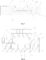
FIG. 4 is a schematic structural view of an optical module in a third packaging fashion according to the third embodiment of the present application; -
FIG. 5 is a schematic structural view of an optical module in a fourth packaging fashion according to the third embodiment of the present application; -
FIG. 6 is a schematic structural view of an optical module in a sixth packaging fashion according to the third embodiment of the present application; -
FIG. 7 is a schematic structural view of an optical module in a fifth packaging fashion according to the third embodiment of the present application; -
FIG. 8 is a schematic structural view of an optical module in a seventh packaging fashion according to the third embodiment of the present application; -
FIG. 9 is a schematic structural view of an optical module in an eighth packaging fashion according to the third embodiment of the present application; -
FIG. 10 is a schematic structural view of an optical module in a ninth packaging fashion according to the third embodiment of the present application; -
FIG. 11 is a schematic structural view of an optical module by an optical module fabrication method according to a fourth embodiment of the present application; -
FIG. 12 is a schematic structural view of a first irregular lens of the optical module by the optical module fabrication method according to the fourth embodiment of the present application; -
FIG. 13 is a schematic structural view of a second irregular lens of the optical module by the optical module fabrication method according to the fourth embodiment of the present application; and -
FIG. 14 is a schematic view of fingerprint identification using the optical module according to first embodiment of the present application. - Reference numerals and denotations thereof:
10-lens; 11-parallel light channel; 21-optical sensor; 211-photosensitive region; 212-metal pad; 22-air gap; 23-substrate; 231-discrete device; 232-tin ball; 233-pad; 24-plastic packaging adhesive; 25-lid; 26-carrier; 27-interposer; 30-filter layer; 60-screen; 81-first die attach film; 82-second die attach film; 83-third die attach film; 84-fourth die attach film; 90-bond wire; 91-wire; 92-bump; and 93-redistribution layer. - For the sake of making the objectives, technical features, and advantages of the present application more apparent and more understandable, the technical solutions according to the embodiments of the present invention are further described in detail with reference to the accompany drawings. Apparently, the embodiments described herein are merely some exemplary ones, rather than all the embodiments of the present application. Based on the embodiments of the present application, all other embodiments derived by persons of ordinary skill in the art without any creative efforts shall fall within the protection scope of the present application.
- Specific implementations of the embodiments of the present application are further described hereinafter with reference to the accompanying drawings of the present application.
- As illustrated in
FIG. 1 , according to this embodiment of the present application, an optical module includes alens 10 and a sensor package. Thelens 10 is positioned at an uppermost position of the optical module and attached to a lower position of aterminal screen 60, and is configured to transmit light passing through thescreen 60; the sensor package includes anoptical sensor 21, where aphotosensitive region 211 is arranged on an upper surface of theoptical sensor 21, and thephotosensitive region 211 is configured to receive light passing through thelens 10; and the sensor package further includes anair gap 22, and thephotosensitive region 211 of theoptical sensor 21 is configured to receive the light passing through thescreen 60 via theair gap 22. - The
optical sensor 21 in the optical module is configured to receive light for use in imaging, and hence generate an image based on the light. Theair gap 22 is arranged in the sensor package including the optical sensor; and the optical sensor is configured to receive light passing through the screen via the air gap, and hence achieve imaging. Theair gap 22 may be filled with a corresponding gaseous medium. The gaseous medium has a low refractive index, and thus may effectively reducing interference to the light for imaging reaching the optical sensor. In this way, accuracy of fingerprint detection and identification is ensured. As compared with imaging based on light passing through other media and reaching the optical sensor in a conventional optical module achieving the same degree of accuracy, with the same thickness, the accuracy of detection and identification is higher. From another perspective, the same accuracy is achieved with a smaller thickness, such that a balancing effect is achieved between accuracy and thickness of the optical module, and the optical module becomes thinner while the accuracy of detection and identification is maintained. - Relative to an optical module formed by bonding a filter layer and a lens using an adhesive in the related art, under the circumstance of the same identification accuracy, the optical module having the
air gap 22 according to this embodiment has an even smaller thickness. In addition, by arranging theair gap 22 between thelens 10 and theoptical sensor 21, an object distance between theoptical sensor 21 and a subject under detection may be increased. As compared with the optical module in which theoptical sensor 21 is directly attached to thelens 10 in the related art, the optical module according to this embodiment may reduce moire in the detection process, and improve the identification accuracy. - Optionally, in this embodiment, the
air gap 22 may be an air interlayer, or may be replaced by a transparent superimposed substance; and in the packaging process, theair gap 22 may be practiced by a suitable packaging process, as long as theair gap 22 is defined between thelens 10 and theoptical sensor 21. Theair gap 22 may have a thickness in the range of 200 to 500 µm, which may improve fingerprint identification performance. - Optionally, the sensor package includes a
substrate 23. According to different actual needs, thesubstrate 23 may be arranged at different positions of the sensor package. - For example, in one specific implementation, as illustrated in
FIG. 1 , thesubstrate 23 is arranged at a lowermost position of the sensor package, and theoptical sensor 21 is positioned on an upper surface of thesubstrate 23. - In another specific implementation, the
substrate 23 may be positioned above theoptical sensor 21. - The
substrate 23 is configured to mount and bear other structures of the sensor package. For example, thesubstrate 23 is configured to mount theoptical sensor 21, and practice electrical connection between theoptical sensor 21 and thesubstrate 23, such that a signal of theoptical sensor 23 is output outside the sensor package via thesubstrate 23. - In this embodiment, the
substrate 23 may be practiced by a combination of a rigid board and a flexible board. In the combination of the rigid board and the flexible board, the surface mount technology (SMT) and reinforced flexible printed circuit (FPC) achieve an even smaller thickness, and thus the thickness of thesubstrate 23 maybe further reduced. In this way, the entire thickness of the optical module is reduced, and requirements on miniaturization, lightening and thinning are accommodated while the accuracy of detection and identification is maintained. Thesubstrate 23 employing the combination of the rigid board and the flexible board may have an entire thickness less than or equal to 1 mm. A circuit configured to transmit the signal of theoptical sensor 21 may be embedded on thesubstrate 23. - Referring to
FIG. 2 , optionally, thesubstrate 23 may be provided with adiscrete device 231 or may be provided with nodiscrete device 231. Thediscrete device 231 includes, for example, a resistor for protecting circuit, or a capacitor for storing energy, or the like. Nevertheless, thediscrete device 231 may be arranged according to the actual needs. Thesubstrate 23 may be connected to other structures via a connection wire 91 (as illustrated inFIG. 1 ) or the like, and thus practice transfer of signals, power and the like. Thesubstrate 23 may also connected to other external structures of the sensor package via a pad or atin ball 232 or the like, and thus practice transfer of signals, power and the like. - In this embodiment, the
optical sensor 21 may be a complementary metal oxide semiconductor (CMOS) sensor. The CMOS sensor includes aphotosensitive region 211 for photosensitive imaging. Theoptical sensor 21 may be integrated with a logic circuit and an optical sensor, and have a function of converting a received optical signal to an electrical signal. By packaging and fabrication, theoptical sensor 21 may lead an electrical signal on the sensor to the exterior of the package, for ease of connection to an external device. - As illustrated in
FIG. 1 , using the scenario where theoptical sensor 21 is positioned on the upper surface of thesubstrate 23 as an example, theoptical sensor 21 may be bonded to the upper surface of thesubstrate 23 via a fourth die attachfilm 84. The fourth die attachfilm 84 below theoptical sensor 21 may have a thickness greater than or equal to 1 µm, and thus may absorb light having a specific wavelength. According to different product requirements, a wavelength range may be determined, and thus a material of the fourth die attach film accommodating the requirements may be selected. - In this embodiment, the
optical sensor 21 may be connected to thesubstrate 23 in a wirebond fashion. Specifically, ametal pad 212 of theoptical sensor 21 may be connected to apad 233 on thesubstrate 23. This connection may involve physical connection or may involve connections of both signals and power. The wirebond fashion achieves a better performance relative to a chip scale package (CSP) fashion, and in this fashion, spherical image interference may not easily occur. In other embodiments, theoptical sensor 21 may also be electrically connected to thesubstrate 23 by bump mounting. - In one specific implementation, the
optical sensor 21 is connected to thesubstrate 23 by abond wire 90 of the optical module. Thebond wire 90 is configured to transfer an electrical signal from theoptical sensor 21 to thesubstrate 23, and a protective die attach film coated outside is arranged on the exterior of thebond wire 90. The protective adhesive layer coating thebond wire 90 may have such characteristics of low shrinkage rate, water-proofing and the like, and thus may better protect thebond wire 90 from environmental impacts. However, the function of the protective adhesive layer is not limited to such protection. - The
bond wire 90 may be a gold wire and/or a copper wire. A specific material of thebond wire 90 may be determined according to the actual needs, cost and the like factors. For example, when a plurality ofbond wires 90 are needed, some may be gold wires and some may be copper wires; or all thebond wires 90 may be fabricated from the same material, both the gold wires or the copper wires or the like, which is not specifically defined herein. - Optionally, the sensor package further includes a
plastic packaging adhesive 24 configured to package and protect theoptical sensor 21 and the like structures. - As illustrated in
FIG. 1 , in one specific implementation, theplastic packaging adhesive 24 defines a support structure surrounding outside theoptical sensor 21, theplastic packaging adhesive 24 is arranged on the upper surface of thesubstrate 23, and an upper surface of theplastic packaging adhesive 24 is above the upper surface of theoptical sensor 21, such that theair gap 22 is defined between theplastic packaging adhesive 24 and theoptical sensor 21. - For example, an opening at least exposing from the
photosensitive region 211 is defined at a portion of theplastic packaging adhesive 24 that is above theoptical sensor 21, such that theair gap 22 is defined between theplastic packaging adhesive 24 and theoptical sensor 23. Still for example, a top of theplastic packaging adhesive 24 is connected to thescreen 60 via a second die attachfilm 82, such that theair gap 22 is defined above theoptical sensor 21. - In this embodiment, the
plastic packaging adhesive 24 is a light shielding material. For example, theplastic packaging adhesive 24 may be in a dark color to achieve the effect of shielding light. However, theplastic packaging adhesive 24 may also be other materials that are capable of absorbing light having a specific wavelength, which is not limited herein. - In this embodiment, the support structure formed by the
plastic packaging adhesive 24 may have a thickness that may be adjusted according to the actual needs, as long as theair gap 22 is defined and has a height accommodating the requirement. - Optionally, the thickness of the
air gap 22 is greater than or equal to 10 µm. In the meantime, since the air gap may be flexibly adjusted based on the thickness of the support structure, as compared with the fabrication processes of the optical module such as a mold process (injection molding and the like fabrication processes), the fashion of forming the support structure by theplastic packaging adhesive 24 makes a more flexible adjustment of the thickness of the optical module and a lower practice cost. - Optionally, the
lens 10 is bonded to a lower position of thescreen 60 via a first die attachfilm 81, thelens 10 corresponds to theoptical sensor 21, and theair gap 22 is positioned below thelens 10 and above theoptical sensor 21. - In this embodiment, the
screen 60 may be an organic light-emitting diode (OLED) material, but is not limited to such material. - In addition, the
screen 60 may have a foam/black adhesive layer on a rear side thereof. For example, the foam or black adhesive layer is attached on a side of thescreen 60 proximal to a metal cathode or on the metal cathode, to prevent light leakage in some occasions, and a region corresponding to thelens 10 on thescreen 60 is a light transmission region for light to pass through. - The second die attach
film 82 is further configured to bond theplastic packaging adhesive 24 to thescreen 60. For example, theplastic packaging adhesive 24 may be bonded to a structure such as the foam or black adhesive layer or the like equipped on the screen via the second die attachfilm 82. The second die attachfilm 82 may be a material having the effect of absorbing light having a specific wavelength to prevent ambient light from passing through the second die attachfilm 82 to cause light leakage. In this way, light leakage is prevented and impacts on the identification accuracy of theoptical sensor 21 are eliminated. - The
lens 10 may absorb light having a specific wavelength, such that the lens achieves a filtering effect. However, thelens 10 is not limited to such effect. Thelens 10 may also be provided with an optical modulation opening or channel. The optical modulation opening has an effect similar to a pinhole in pinhole imaging. The channel allows the light to pass through to form a collimated light, and obliquely incident light may collide with a wall of the channel when passing through thelens 10 and thus may be absorbed, such that the light passing through thelens 10 is a direct light. - The first die attach
film 81 for bonding thelens 10 may be fabricated by a material that is capable of transmitting light having a specific wavelength, such that the light transmission is ensured while thelens 10 is bonded. In this way, detection and identification of the optical module may not be affected. - The
lens 10 is a light path modulation device, and practices transmission of special light by modulating a light path. Thelens 10 is configured to improve the fingerprint identification performance, and may be arranged below thescreen 60 or above theoptical sensor 21. In addition, thelens 10 may be integrated in the package by packaging, or may be added during subsequent assembling of the module. Thelens 10 needs to cover the photosensitive region of theoptical sensor 21. When the optical module includes afilter layer 30, thelens 10 may be arranged above thefilter layer 30 or arranged below thefilter layer 30. Optionally, the first die attachfilm 81 has a thickness less than or equal to 200 µm. - As illustrated in
FIG. 2 , in another specific implementation, the sensor package further includes alid 25. Thelid 25 is positioned on the upper surface of theplastic packaging adhesive 24, and theair gap 22 is defined between thelid 25 and theoptical sensor 21. - The
lid 25 is a lid provided with an opening, and the opening on thelid 25 corresponds to thephotosensitive region 211 of theoptical sensor 21, such that the air gap is defined between thelid 25 and theoptical sensor 21. - In still another specific implementation, the
substrate 23 is provided with an opening, theoptical sensor 21 is positioned in the opening on thesubstrate 23, the upper surface of thesubstrate 23 is above the upper surface of theoptical sensor 21, and theair gap 22 is defined between thesubstrate 23 and theoptical sensor 21. - The above describes the optical module according to the embodiment of the present application using the scenario where the
substrate 23 is used as a bearer as an example. However, in another feasible implementation, thesubstrate 23 may be replaced by acarrier 26. As illustrated inFIG. 8 to FIG. 10 , the sensor package further includes thecarrier 26, where thecarrier 26 is positioned at a lowermost position of the sensor package. A side surface of thecarrier 26 coats theoptical sensor 21, which increases an area of the package besides theoptical sensor 21, and achieves effects of expanding a fan-out redistribution region and protecting the chip. Thecarrier 26 may be a silicon sheet, a plastic packaging material or a substrate. A groove for receiving theoptical sensor 21 may be formed by a trenching process, or theoptical sensor 21 may be coated by an open mold process. - A structure having effects of bearing and protecting the
optical sensor 21 similar to thecarrier 26 may be formed by coating theoptical sensor 21 with theplastic packaging adhesive 24. Thecarrier 26 may also be fabricated from other materials by other fabrication processes. Using fabrication of thecarrier 26 using theplastic packaging adhesive 24 as an example, theoptical sensor 21 is positioned on the upper surface of theplastic packaging adhesive 24, and an upper surface of the carrier 26 (that is, the plastic packaging adhesive 24) is flush with the upper surface of theoptical sensor 21. - Using fabrication of the
carrier 26 using other materials as an example, thecarrier 26 is provided with an opening, theoptical sensor 21 is positioned in the opening on thecarrier 26, and an upper surface of thecarrier 26 is flush with the upper surface of theoptical sensor 21. - An
interposer 27 or alid 25 is arranged over theplastic packaging adhesive 24 or thecarrier 26, where theair gap 22 is defined between the interposer 27 or thelid 25 and theoptical sensor 21. - The
interposer 27 or thelid 25 is a structure having an opening, and theair gap 22 may be defined between the opening of theinterposer 27 or thelid 25 and theoptical sensor 21. - Optionally, the optical module further includes a
filter layer 30, where thefilter layer 30 is positioned between thelens 10 and theoptical sensor 21. - In this embodiment, the
filter layer 30 may be a filter sheet. The filter sheet has an effect of absorbing light having a specific wavelength, and may filter light according to the actual needs. The filter sheet is equivalent to a bandpass filter sheet. Thefilter layer 30 may at least filter a portion of the light, such that undesired light is prevented from causing interference and impacts on the detection and identification of theoptical sensor 21. For example, during fingerprint identification, if a user places his or her finger randomly, a portion of ambient light may be transmitted to the optical module. If the ambient light, together with light reflected by the finger, reaches theoptical sensor 21 at the same time, identification by theoptical sensor 21 may be inaccurate or may fail. In this case, the undesired light generated by the ambient light needs to be removed, such that accuracy of the identification is not affected. - In one specific implementation, a lower part of the
filter layer 30 is bonded to theoptical sensor 21 via a third die attach film 83 (as illustrated inFIG. 1 ) which is capable of transmitting light having a wavelength in a specific range. The specific range may be specifically determined according to different product requirements. If thefilter layer 30 is a filter sheet, at least one surface of the filter sheet may be provided with a reflective plating layer which may reflect light having some wavelengths, such that the undesired light is prevented from passing through. The light to be filtered herein is light which adversely affects the accuracy of identification. Upper and lower surfaces of the filter sheet may be both provided with a reflective plating layer, or either of the upper and lower surfaces of the filter sheet may be provided with a reflective plating layer, or neither of the upper and lower surfaces of the filter sheet is provided with a reflective plating layer. - In this embodiment, the
filter layer 30 covers thephotosensitive region 211 of theoptical sensor 21, and is arranged under thelens 10. An area of thefilter layer 30 is greater than or equal to the area of thephotosensitive region 211 of theoptical sensor 21, and the area of the lens is greater than or equal to the area of thefilter layer 30. In this way, it may be ensured that the light reaching thefilter layer 30 is processed by the lens 10 (for example, focusing processing). The area of thefilter layer 30 is greater than or equal to the area of thephotosensitive region 211 of theoptical sensor 21, and thefilter layer 30 covers thephotosensitive region 211 of theoptical sensor 21, such that the light reaching thephotosensitive region 211 of theoptical sensor 21 is processed by thefilter layer 30 to ensure the accuracy of detection and identification of the optical module. - The
filter layer 30 may employ a transparent or semi-transparent material as a base material, and achieve an effect of cutting of light in a specific waveband by coating on the surface of thefilter layer 30. Thefilter layer 30 is arranged above theoptical sensor 21. Alternatively, thefilter layer 30 may employ theoptical sensor 21 as a base material, and achieve an effect of filtering light by directly coating on the surface ofoptical sensor 21. Thefilter layer 30 maintains optical signal transfer with theoptical sensor 21, and may be integrated in the package by packaging or may be added during subsequent assembling of the module. Thefilter layer 30 may be arranged below thescreen 60 and above theoptical sensor 21. Thefilter layer 30 may be integrated in the package by packaging, or may be arranged externally independently and added during assembling of the module. In addition, thefilter layer 30 may not be arranged according to the actual needs. Thefilter layer 30 is sized to cover thephotosensitive region 211 of theoptical sensor 21. - The
lens 10 may be attached to thefilter layer 30 via a transparent die attach film (DAF), or frame attached to thefilter layer 30 via an adhesive film, or arranged externally directly and added during assembling of the module. Thefilter layer 30 may be arranged above theair gap 22 by attachment via the transparent DAF or by frame attachment via the adhesive film, or arranged externally and added during assembling of the module. - It should be noted that when the optical module includes the
filter layer 30, during electrically connecting theoptical sensor 21 to thesubstrate 23 via thebond wire 90, as illustrated inFIG. 1 , a radian height of the bond wire 90is less than a sum of the thicknesses of theoptical sensor 21 and thefilter layer 30. That is, a highest point at a bending part of thebond wire 90 does not exceed a top surface of thefilter layer 30. - As illustrated in
FIG. 1 , a total thickness of the entire structure of the optical module is greater than 0.8 mm, and may not exceed 1.1 mm. A value range of the thickness of thesubstrate 23 is 50 to 500µm, preferably, 400 µm. The thickness of the support structure formed by theplastic packaging adhesive 24 is determined based on the height of theair gap 22, for example, 500 µm. A value range of the thickness of the second die attach film 80 is 10 µm to 1 mm, preferably, 200 µm. A value range of the thickness of thelens 10 is 50 to 400 µm, preferably 150 µm. A value range of the thickness of the first die attachfilm 81 between thelens 10 and thescreen 60 is 0 to 100 µm, preferably, 50 µm, where the smaller the thickness, the better. A value range of the thickness of theair gap 22 is greater than 10 µm, preferably, 250 µm, where in an ideal state, the greater the thickness, the better. A value range of the thickness of thefilter layer 30 is 50 to 400 µm, preferably 110 µm. A value range of the thickness of theoptical sensor 21 is 25 to 650 µm, preferably 100 µm. A value range of the thickness of the third die attachfilm 83 between theoptical sensor 21 and thefilter layer 30 is greater than 10 µm, preferably, 20 µm. A value range of the thickness of the fourth die attachfilm 84 between theoptical sensor 21 and thesubstrate 23 is greater than 10 µm, preferably, 20 µm. - The above dimensions are merely exemplary, and the specific dimensions may be specifically determined based on the process requirements.
- In this embodiment, an optical module is provided. Different from the optical module in the first embodiment, in the optical module according to this embodiment, the air gap is positioned outside the sensor package.
- Based on this, the optical module according to this embodiment includes a
lens 10 and a sensor package. Thelens 10 is positioned at an uppermost position of the optical module and attached to a lower position of aterminal screen 60, and is configured to transmit light passing through thescreen 60; the sensor package includes anoptical sensor 21, where aphotosensitive region 211 is arranged on an upper surface of theoptical sensor 21, and thephotosensitive region 211 is configured to receive light passing through thelens 10; and anair gap 22 is defined between thelens 10 and the sensor package, and thephotosensitive region 211 of theoptical sensor 21 is configured to receive the light passing through thescreen 60 via theair gap 22. - In this embodiment, the optical module includes the
air gap 22, where theair gap 22 may be filled with a corresponding gaseous medium. The gaseous medium has a low refractive index, and thus may effectively reducing interference to the light for imaging reaching the optical sensor. In this way, accuracy of fingerprint detection and identification is ensured. As compared with imaging based on light passing through other media and reaching the optical sensor in a conventional optical module achieving the same degree of accuracy, with the same thickness, the accuracy of detection and identification is higher. From another perspective, the same accuracy is achieved with a smaller thickness, such that a balancing effect is achieved between accuracy and thickness of the optical module, and the optical module becomes thinner while the accuracy of detection and identification is maintained. - In this embodiment, the sensor package may further include a
substrate 23, afilter layer 30, aplastic packaging adhesive 24 and the like in addition to theoptical sensor 21. Theoptical sensor 21 is arranged on an upper surface of thesubstrate 23, and ametal pad 212 of theoptical sensor 21 is connected to a pad on thesubstrate 23 via abond wire 90. The filter layer is arranged on an upper surface of theoptical sensor 21, and at least covers thephotosensitive region 211. Theplastic packaging adhesive 24 packages thesubstrate 23, thefilter layer 30 and theoptical sensor 21, and an upper surface of theplastic packaging adhesive 24 is flush with an upper surface of thefilter layer 30. - The functions of the
substrate 23, thefilter layer 30 and theplastic packaging adhesive 24 in this embodiment are the same as the functions of thesubstrate 23, thefilter layer 30 and theplastic packaging adhesive 24 in the first embodiment, which are thus not described herein any further. - Optionally, as illustrated in
FIG. 12 , the optical module further includes alid 25, where thelid 25 is positioned between the lens and the sensor package, and thelid 25 is a lid provided with an opening, and theair gap 22 is defined between thelens 10 and the sensor package via the opening on thelid 25. Nevertheless, in other embodiments, thelid 25 may be other structures, as long as theair gap 22 is defined between the lens and the sensor package. - Nevertheless, a groove may be directly machined on the
lens 10, such that theair gap 22 is defined between thelens 10 and the sensor package via the groove on thelens 10. - In this embodiment, an optical module fabrication method is provided. The method is applied to fabrication of the optical module according to the first embodiment or the second embodiment.
- The optical module fabrication method according to this embodiment includes: packaging an
optical sensor 21 to form a sensor package having anair gap 22, where aphotosensitive region 211 configured to receive light is arranged on an upper surface of theoptical sensor 21, and theair gap 22 in the sensor package is positioned above thephotosensitive region 211 of theoptical sensor 21; and forming an optical module by using the sensor package and alens 10 configured to transmit light, where thelens 10 is positioned at an uppermost position of the optical module. - The optical module fabricated by using the optical module fabrication method has a high degree of packaging integration. Since the optical module includes an
air gap 22 which may be filled with a gaseous medium having low refractive index, for example, air, interference to the light for imaging that reaches the optical sensor may be effectively reduced, accuracy of fingerprint detection and identification is ensured, and meanwhile an entire thickness of the optical module may be reduced. In addition, integrated packaging of theoptical sensor 21 and theair gap 22 improves the degree of package integration, reduces a total thickness of the optical module and enhances fingerprint image quality. - A structure by which the optical module fabricated by using the optical module fabrication method according to this embodiment is applied to a mobile terminal is as illustrated in
FIG. 14 . The optical module may be applied to a full display mobile terminal. The optical module for fingerprint identification is mounted below ascreen 60. Light emitted by thescreen 60 is irradiated to a fingerprint on the surface of a finger and then reflected to a surface of thelens 10, subjected to light path modulation (focusing) by thelens 10 and passed through the air gap 22 (the light may be passed through thefilter layer 30 according to the actual needs), and finally imaged on the surface of theoptical sensor 21. Finally, theoptical sensor 21 captures an optical signal and converts the optical signal into an electrical signal, and thus acquires the fingerprint. - In practice, the above optical module may be fabricated by using any one of the packaging fashions hereinafter.
- Before the
optical sensor 21 is packaged to form the sensor package having theair gap 22, theoptical sensor 21 is firstly connected to asubstrate 23. - For example, the
optical sensor 21 may be bonded to thesubstrate 23, and theoptical sensor 21 is electrically connected to thesubstrate 23. - In a specific implementation, the optical sensor 21 (which may be a singulated sensor chip) is bonded to an upper surface of the
substrate 23 via an epoxy resin or a die attach film (DAF), and the photosensitive region of theoptical sensor 21 is made to face upward. Theoptical sensor 21 is electrically connected to thesubstrate 23 via abond wire 90. A fabricated optical module is as illustrated inFIG. 2 and FIG. 3 . - Optionally, the
optical sensor 21 may be packaged by a first packaging process, and a sensor package having theair gap 22 is formed, such that theoptical sensor 21 is packaged and the sensor package having theair gap 22 is formed. - In a specific implementation, a
filter layer 30 may be arranged on theoptical sensor 21 according to the actual needs. If thefilter layer 30 is arranged, the method further includes: attaching thefilter layer 30 on the upper surface of theoptical sensor 21 via a transparent adhesive or a transparent DAF, such that thefilter layer 30 at least covers thephotosensitive region 211 of theoptical sensor 21. In this way, theoptical sensor 21 is positioned between thefilter layer 30 and thesubstrate 23. - The first packaging process may be an irregular open mold process (a molding process which may present a predefined shape for a plastic packaging adhesive upon the molding). The
optical sensor 21, thefilter layer 30 and thesubstrate 23 are packaged using aplastic packaging adhesive 24, and theair gap 22 is defined between theplastic packaging adhesive 24 and theoptical sensor 21. During plastic packaging by the irregular open mold process, an upper surface of thefilter layer 30 is made to expose outside, such that theair gap 22 is defined. Atin ball 232 may be mounted on a pad on a lower surface of the substrate 23 (whether to mount a tin ball may be determined according to the actual needs, or the pad may be directly reserved), and the package is cut. A sensor package upon the packaging is as illustrated inFIG. 3 . - The
lens 10 is bonded to an upper surface of a singulated sensor package upon the cutting to form an optical module, and thelens 10 is positioned at an uppermost position of the optical module. - In this packaging fashion, the packaging process is similar to that in the packaging fashion 1. Therefore, the identical packaging process is not described herein any further. Instead, only the different packaging process is described hereinafter.
- In this packaging fashion, the first packaging process may be an open mold process (a molding process which may cause a surface of a chip upon the molding to expose outside). The
optical sensor 21, thefilter layer 30 and thesubstrate 23 are packaged using theplastic packaging adhesive 24, the upper surface of thefilter layer 30 is flush with the upper surface of theplastic packaging adhesive 24, and theplastic packaging adhesive 24 is exposed outside. Alid 25 is bonded to the upper surface of theplastic packaging adhesive 24, such that theair gap 22 is defined between thelid 25 and theoptical sensor 21, and the sensor package is formed. Thelid 25 arranged on the upper surface of theplastic packaging adhesive 24 is a lid having a through hole, and theair gap 22 is defined at the through hole on thelid 25. Thetin ball 232 may be mounted on the pad on the lower surface of thesubstrate 23, and finally the package is cut. A sensor package upon the packaging is as illustrated inFIG. 2 . - The
lens 10 is bonded to an upper surface of a singulated sensor package upon the cutting to form an optical module, and thelens 10 is positioned at an uppermost position of the optical module. - In this packaging fashion, the packaging process in which the
optical sensor 21 is mainly packaged to form the sensor package having theair gap 22 is mainly described. The process of connecting theoptical sensor 21 to thesubstrate 23 may be the same as that in the first packaging fashion, which is thus not described herein any further. The packaging process includes: packaging theoptical sensor 21 by the first packaging process, and forming the sensor package having theair gap 22. An optical module upon the packaging is as illustrated inFIG. 4 . - A filler layer is arranged on the upper surface of the
filter layer 30. The filler layer has a thickness that may be determined based on a height of the air gap to be defined, for example, 200 to 500 µm. The filler layer may be fabricated from an photosensitive material, for ease of peeling. - The
filter layer 30 having the filler layer is bonded to the upper surface of theoptical sensor 21, such that thefilter layer 30 at least covers thephotosensitive region 211 of theoptical sensor 21, and theoptical sensor 21 is positioned between thefilter layer 30 and thesubstrate 23. Theoptical sensor 21 and thefilter layer 30 may be bonded to each other via a transparent DAF or the like. - The first packaging process is an open mold process. By the first packaging process, the
optical sensor 21, the filler layer, thefilter layer 30 and thesubstrate 30 are packaged using theplastic packaging adhesive 24. The filler layer is peeled, such that theair gap 22 is defined theplastic packaging adhesive 24 and theoptical sensor 21, and the sensor package is formed. Specifically, the filler layer may be peeled using a peeling agent which dissolves the filler layer and only maintains theair gap 22. Finally, cutting is performed to cut the package into singulated packages. - On the resulted sensor package, the
lens 10 with a paralleloptical channel 11 being etched on a lens base is combined to the sensor package via, for example, frame attachment. - As illustrated in
FIG. 5 , in this packaging fashion, in the optical module fabrication method, the process of bonding theoptical sensor 21 to thesubstrate 23, and electrically connecting theoptical sensor 21 connected to thesubstrate 23 includes:
providing a through hole on thesubstrate 23; mounting a bump on a wafer of an optical sensor chip by a bump process (also referred to as a ball mounting process), and forming theoptical sensor 21 by dicing; and connecting theoptical sensor 21 to thesubstrate 23 by a flip chip process, and electrically connecting theoptical sensor 21 to thesubstrate 23 via the bump. In this case, a metal pad 121 of theoptical sensor 21 is electrically connected to apad 233 on thesubstrate 23 via the bump. - In the optical module fabrication method, the process of packaging the
optical sensor 21 by the first packaging process, and forming the optical package having theair gap 22 includes:
using a mold process (an injection molding process which packages a chip and a package carrier together using a molding mould, and then injects a plastic packaging adhesive to the mould to achieve plastic packaging) as the first packaging process); sealing theoptical sensor 21 by underfill dispensing, for example, forming a fourth die attachfilm 84 by underfill dispensing, sealing theoptical sensor 21 and thesubstrate 23 via the fourth die attachfilm 84, and at least exposing the formed fourth die attachfilm 84 out of the photosensitive region of theoptical sensor 21; packaging theoptical sensor 21 and thesubstrate 23 by the first packaging process, defining theair gap 22 between thesubstrate 23 and theoptical sensor 21, and forming the sensor package; and finally, cutting the package to form singulated sensor packages. - The
lens 10 is bonded to the singulated sensor package to form an optical module, and thelens 10 is positioned at an uppermost position of the optical module. - As illustrated in
FIG. 7 , in the optical module fabrication method, the process of bonding theoptical sensor 21 to thesubstrate 23, and electrically connecting theoptical sensor 21 connected to thesubstrate 23 includes: - providing a through hole on the
substrate 23. fabricating an optical sensor chip by a through silicon via (TSV) process, where the TSV process is carried out for a wafer for the optical sensor chip; electrically connecting ametal pad 212 on an upper surface of the optical sensor chip to a redistribution pad on a lower surface of the optical sensor chip via a TSV; and - bonding the optical sensor chip to the
substrate 23, and electrically connecting the optical sensor chip to thesubstrate 23 via abond wire 90. - In a specific implementation, the
filter layer 30 is bonded to thesubstrate 23. The optical sensor chip is bonded to thefilter layer 30, and thefilter layer 30 at least covers aphotosensitive region 211 of the corresponding optical sensor chip. The redistribution pad of the optical sensor chip is electrically connected to thesubstrate 23 via thebond wire 90. - In the optical module fabrication method, the process of packaging the
optical sensor 21 by the first packaging process, and forming the optical package having theair gap 22 includes:
using a mold process as the first packaging process; and packaging the optical sensor chip, thefilter layer 30 and thesubstrate 23 using theplastic packaging adhesive 24 by the first packaging process, and forming the sensor package by singulated cutting, where sensor chips in various sensor packages areoptical sensors 21, and theair gap 22 is defined between thesubstrate 23 and theoptical sensor 21, for example, theair gap 22 is defined above thefilter layer 30 at the through hole on thesubstrate 23 inFIG. 7 . - The
lens 10 is bonded to the sensor package formed upon the cutting to form an optical module, and thelens 10 is positioned at an uppermost position of the optical module. - As illustrated in
FIG. 6 , in the optical module fabrication method, before theoptical sensor 21 is packaged to form the sensor package having theair gap 22, the optical module fabrication method further includes providing a through hole on thesubstrate 23. - In the optical module fabrication method, the process of packaging the
optical sensor 21 to form the sensor package having theair gap 22 includes: packaging the optical sensor chip by a fan-out process (by the fan-out process, an electrical signal may be led out to the exterior of the chip region), and forming a redistribution pad, where the redistribution pad is electrically connected to a metal pad on the optical sensor chip; mounting abump 92 on the redistribution pad; electrically connecting the optical sensor chip to thesubstrate 23 by an SMT process; forming the fourth die attachfilm 84 by underfill dispensing, sealing the optical sensor chip via the fourth die attachfilm 84, and exposing thephotosensitive region 211 of the optical sensor chip from the through hole on thesubstrate 23, where thefilter layer 30 may be bonded to an upper surface of thephotosensitive region 211 according to the filtering needs; and forming the sensor package by singulated cutting. - Sensor chips in various sensor packages are
optical sensors 21, and theair gap 22 is defined between thesubstrate 23 and theoptical sensor 21. - The
lens 10 is bonded to the sensor package formed upon the cutting to form an optical module, and thelens 10 is positioned at an uppermost position of the optical module. - As illustrated in
FIG. 8 , in this packaging process, in the optical module fabrication method, the forming theoptical sensor 21 to form the sensor package having theair gap 22 includes:
thinning and dicing the wafer of the optical sensor chip, and forming a singulatedoptical sensor 21; and connecting theoptical sensor 21 to acarrier 26, and causing an upper surface of theoptical sensor 21 to be flush with an upper surface of thecarrier 26. - As illustrated in
FIG. 8 , thecarrier 26 may be a carrier fabricated from any suitable material. In a specific implementation, theoptical sensor 21 may be connected to thecarrier 26 via an opening provided on thecarrier 26, and theoptical sensor 21 is bonded to the opening, such that the upper surface of theoptical sensor 21 is flush with an upper surface of thecarrier 26. A first insulation layer may also be formed on the upper surface of thecarrier 26 and an upper surface of themetal pad 212 of theoptical sensor 21 to ensure insulation and prevent electrical leakage or short circuit or the like. Aredistribution layer 93 electrically connected to themetal pad 212 of theoptical sensor 21 is formed on the first insulation layer by the fan-out process. A second insulation layer is formed on the redistribution layer. - It should be noted that the redistribution layer, that is, RDL, leads out the electrical signal of the optical sensor chip by metal redistribution, and is arranged on the surface of the optical sensor chip and the surface of the carrier (that is, the carrier 26). The RDL leads out the electrical signal of the
optical sensor 21 above a non-photosensitive region by the metal redistribution fabricated by the fan-out process, which may be arranged on an upper surface of the non-photosensitive region on the surface of the chip or may be arranged on the upper surface of the carrier. Theoptical sensor 21 leads the electrical signal to the upper surface of the carrier by the RDL, or leads the electrical signal to an upper surface of another structure by the RDL. - An
interposer 27 having a through hole is bonded to the second insulation layer. A bump is mounted on theinterposer 27, such that thebump 92 is electrically connected to the redistribution layer 93 (RDL wiring), the sensor package is formed, and theair gap 22 is defined between theinterposer 27 and theoptical sensor 21. For example, as illustrated inFIG. 8 , theair gap 22 is defined at the through hole above thephotosensitive region 211 of theoptical sensor 21. - It should be noted that to ensure that the
photosensitive region 211 is capable of receiving light and implementing the functionality thereof, theredistribution layer 93 needs to be arranged to avoid the photosensitive region, which may be expanded on an upper surface of the first insulation layer. The second insulation layer may achieve an effect of protecting theredistribution layer 93. Thebump 92 may be interconnected to an external device, for example, a circuit board, to practice electrical connection. - The first insulation layer and the second insulation layer are used to practice insulation protection, and are arranged above and below the RDL. The first insulation layer and the second insulation layer may cover the
photosensitive region 211 of theoptical sensor 21, or may not cover thephotosensitive region 211 of theoptical sensor 21. The materials of the insulation layers may be only reserved in the non-photosensitive region of theoptical sensor 21 in an exposure and development fashion, or may be transparent materials and reserved above the photosensitive region of theoptical sensor 21. - The bump may practice electrical connection between the
optical sensor 21 and an external device, and is arranged on the surface of the package. The bump is arranged above the non-photosensitive region, and is configured to be connected to the external device to practice the electrical connection to the optical sensor chip. Alternatively, the bump may not be arranged according to the actual needs, and the pad is reserved. - The interposer may be a silicon sheet, an organic substance or a substrate, which may practice transfer of the electrical signal from one side to the other side.
- The hollow lid may be a plastic packaging adhesive or a metal sheet.
- The
air gap 22 may be replaced by a transparent superimposed layer (for example, glass), and the transparent superimposed layer is directly attached to an upper position of theoptical sensor 21 or thefilter layer 30. - After the sensor package is formed, the
lens 10 and thefilter layer 30 may be attached, via a transparent DAF or via frame attachment, to an upper position of an irregular fan-out package formed by the fan-out process to form the optical module. In the optical module, it needs to be ensured that thelens 10 and thefilter layer 30 cover the entirephotosensitive region 211. - In this packaging process, the differences from the seventh packaging fashion lie in the material of the
carrier 26 and the fashion of connection to theoptical sensor 21. The other packing processes may be the same as those in the seventh packaging fashion, or only adaptively adjusted, which are thus not described herein any further. - As illustrated in
FIG. 9 , in a specific implementation, in the optical module fabrication method, the connecting theoptical sensor 21 to thecarrier 26, and causing the upper surface of theoptical sensor 21 to be flush with the upper surface of thecarrier 26 includes:
Packaging theoptical sensor 21 using the plastic packaging adhesive 24 (for example, an EMC plastic packaging material) by the open mold process, and causing theplastic packaging adhesive 24 to form thecarrier 26 below theoptical sensor 21, such that the upper surface of thecarrier 26 is flush with the upper surface of theoptical sensor 21. - As illustrated in
FIG. 10 , in this packaging process, the differences from the seventh packaging fashion mainly lie in the process of packaging theoptical sensor 21 to form the sensor package having theair gap 22. The other processes are the same as or similar to those in the seventh packaging fashion, which are thus not described herein any further. The process of packaging theoptical sensor 21 to form the sensor package having theair gap 22 includes:
bonding thelid 25 having the through hole to the second insulation layer; and providing an opening on the second insulating layer and mounting a bump in the opening, such that the bump is electrically connected to the redistribution layer, the sensor package is formed, and theair gap 22 is defined between thelid 25 and theoptical sensor 21. - In this embodiment, an optical module fabrication method is provided. The method is applied to fabrication of the optical module according to the first embodiment or the second embodiment. In this embodiment, the optical module fabrication method is different from the optical module fabrication method according to the third embodiment in that the
air gap 22 is defined on thelens 10, and the sensor package may be a common package. - The optical module fabrication method according to this embodiment includes: packaging an
optical sensor 21 to form a sensor package, where aphotosensitive region 211 configured to receive light is arranged on an upper surface of theoptical sensor 21, and anair gap 22 is defined below alens 10 configured to transmit light; and forming an optical module by using the sensor package and thelens 10 having theair gap 22, where thelens 10 is positioned at an uppermost position of the optical module, and aphotosensitive region 211 of theoptical sensor 21 is configured to receive light via theair gap 22. - In the optical module fabrication method, a degree of packaging integration of the optical module may be improved, a packaging thickness may be reduced, and the
air gap 22 is additionally arranged. In addition, integrated packaging of theoptical sensor 21 and theair gap 22 improves the degree of package integration, reduces a total thickness of the optical module and enhances fingerprint image quality. Theair gap 22 of the optical module may be defined on thelens 10 whereas the sensor package employs an LGA packaging structure, such that packaging difficulties are lowered. - In a specific implementation, the defining the
air gap 22 below thelens 10 configured to transmit light includes: bonding alid 25 having a through hole to a lower position of thelens 10, and defining theair gap 22 at the through hole of thelid 25. - Specifically, for example, on a lens substrate, a parallel
light channel 11 is machined by dry etching (or laser), and thelens 10 is generated. A layer oflid 25 having the through hole with a specific thickness (for example, 200 to 500 µm is attached to thelens 10 by sticking (or bonding). Cutting is performed to cut the irregular lens into singulated ones, and the irregular singulated lens is as illustrated inFIG. 12 . - In a specific implementation, the defining the
air gap 22 below thelens 10 configured to transmit light includes: machining a groove at a lower position of thelens 10, and defining theair gap 22 at the groove. - Specifically, for example, a groove is machined firstly on a lens substrate by dry etching (or wet etching or the like); then a parallel
light channel 11 is machined on an upper surface of the groove; and finally, cutting is performed to cut the irregular lens into singulated ones, and the singulated irregular lens formed upon the cutting is as illustrated inFIG. 13 . - The process of forming the sensor package includes: attaching a
substrate 23, theoptical sensor 21 and afilter layer 30, completing fabrication of the bond wire; electrically connecting ametal pad 212 of theoptical sensor 21 to asubstrate 23; then packaging by an open mold process such that a top surface of thefilter layer 30 is exposed from aplastic packaging adhesive 24; and finally cutting the package into singulated ones. - After fabrications of these two parts are both completed, the sensor package and the
lens 10 are combined via a transparent DAF or via frame attachment, and thus the optical module as illustrated inFIG. 11 is practiced. - In this embodiment, a terminal device is provided. The terminal device includes the above described optical module. The terminal device employs the above described optical module, such that the volume of the terminal device is reduced, and the terminal device is lightened and thinned while performance of the terminal device is ensured.
- In this way, the volume of the terminal device having the above described optical module is reduced, and lightening and thinning of the terminal device are achieved while the accuracy of identification is maintained.
- The terminal device may be a mobile terminal device, for example, a mobile phone, a tablet computer, a video recorder, a camera or the like. Still, the terminal device may also be an attendance machine or the like.
- Finally, it should be noted that the above embodiments are merely intended to describe the technical solutions of the embodiments of the present application, instead of limiting the present application. Although the present application is described in detail with reference to the above embodiments, persons of ordinary skill in the art should understand that various modifications may be made to the technical solutions described in the above embodiments or equivalent replacements may be made to some technical features thereof, without departing from the spirit and scope of the technical solutions of the embodiments of the present application.
Claims (34)
- An optical module, comprising a lens and a sensor package; wherein
the lens is positioned at an uppermost position of the optical module and arranged under a lower position of a terminal screen, and is configured to transmit light passing through the screen;
the sensor package comprises an optical sensor, a photosensitive region being arranged on an upper surface of the optical sensor, the photosensitive region being configured to receive light passing through the lens; and
the sensor package further comprises an air gap, and the photosensitive region of the optical sensor is configured to receive the light passing through the screen via the air gap. - The optical module according to claim 1, wherein the sensor package further comprises a substrate, the substrate being positioned at a lowermost position of the sensor package.
- The optical module according to claim 2, wherein the optical sensor is positioned on an upper surface of the substrate, and the sensor package further comprises a plastic packaging adhesive.
- The optical module according to claim 3, wherein an upper surface of the plastic packaging adhesive is above the upper surface of the optical sensor; and an air gap is provided in the sensor package, wherein the air gap is formed between the plastic packaging adhesive and the optical sensor.
- The optical module according to claim 3, wherein
the sensor package further includes a lid, the lid being positioned on an upper surface of the plastic packaging adhesive; the air gap in the sensor package is formed by: defining an air gap between the plastic packaging adhesive and the optical sensor. - The optical module according to claim 2, wherein the substrate is provided with an opening, the optical sensor is positioned in the opening of the substrate, and an upper surface of the substrate is above the upper surface of the optical sensor; and
an air gap is provided in the sensor package, wherein the air gap is formed between the substrate and the optical sensor. - The optical module according to claim 1, wherein the sensor package further comprises a carrier positioned at a lowermost position of the sensor package.
- The optical module according to claim 7, wherein the sensor package further comprises a plastic packaging adhesive, the optical sensor is positioned on an upper surface of the carrier, and an upper surface of the plastic packaging adhesive is flush with the upper surface of the optical sensor; and
an interposer or a lid is arranged above the plastic packaging adhesive, and
an air gap is provided in the sensor package, wherein the air gap is formed between the interposer or the lid and the optical sensor. - The optical module according to claim 7, wherein the carrier is provided with an opening, the optical sensor is positioned in the opening of the carrier, and an upper surface of the carrier is flush with the upper surface of the optical sensor; and
an interposer or a lid is arranged above of the carrier, and
an air gap is provided in the sensor package, wherein the air gap is formed between the interposer or the lid and the optical sensor. - The optical module according to any one of claims 1 to 9, further comprising a filter layer; wherein
the filter layer is positioned between the lens and the optical sensor. - An optical module, comprising a lens and a sensor package; wherein
the lens is positioned at an uppermost position of the optical module and attached to a lower position of a terminal screen, and is configured to transmit light passing through the screen;
the sensor package comprises an optical sensor, a photosensitive region being arranged on an upper surface of the optical sensor, the photosensitive region being configured to receive light passing through the lens; and
an air gap is defined between the lens and the sensor package, and the photosensitive region of the optical sensor is configured to receive the light passing through the screen via the air gap. - The optical module according to claim 11, further comprising a lid; wherein the lid is positioned between the lens and the sensor package; and
an air gap is provided in the sensor package, wherein the air gap is formed between the lens and the sensor package via the lid. - The optical module according to claim 11 or 12, further comprising a filter layer; wherein
the filter layer is positioned between the lens and the optical sensor, and an area of the filter layer is greater than or equal to an area of the photosensitive region of the optical sensor. - An optical module fabrication method, comprising:packaging an optical sensor to form a sensor package having an air gap, wherein a photosensitive region configured to receive light is arranged on an upper surface of the optical sensor, and the air gap in the sensor package is positioned above the photosensitive region of the optical sensor; andforming an optical module by using the sensor package and a lens configured to transmit light, wherein the lens is positioned at an uppermost position of the optical module.
- The method according to claim 14, wherein prior to the packaging an optical sensor to form a sensor package having an air gap, the method further comprises:
connecting the optical sensor to a substrate. - The method according to claim 15, wherein the connecting the optical sensor to a substrate comprises:bonding the optical sensor to the substrate, and electrically connecting the optical sensor to the substrate; andthe packaging an optical sensor to form a sensor package having an air gap comprises:
packaging the optical sensor by a first packaging process, and forming the sensor package having an air gap. - The method according to claim 16, wherein the electrically connecting the optical sensor to the substrate comprises:
electrically connecting the optical sensor to the substrate via a bond wire. - The method according to claim 17, wherein the packaging the optical sensor by a first packaging process, and forming the sensor package having an air gap comprises:bonding a filter layer to the upper surface of the optical sensor, such that the filter layer at least covers the photosensitive region of the optical sensor, and the optical sensor is positioned between the filter layer and the substrate; andpackaging the optical sensor, the filter layer and the substrate using a plastic packaging adhesive by the first packaging process, forming the sensor package, and defining an air gap between the plastic packaging adhesive and the optical sensor, wherein the first packaging process is an irregular open mold process.
- The method according to claim 17, wherein the packaging the optical sensor by a first packaging process, and forming the sensor package having an air gap comprises:arranging a filler layer on an upper surface of a filter layer;bonding the filter layer to the upper surface of the optical sensor, such that the filter layer at least covers the photosensitive region of the optical sensor, and the optical sensor is positioned between the filter layer and the substrate; andpackaging the optical sensor, the filler layer, the filter layer and the substrate using a plastic packaging adhesive by the first packaging process, wherein the first packaging process is an open mold process; andpeeling the filler layer, such that the air gap is defined between the plastic packaging adhesive and the optical sensor, and the sensor package is formed.
- The method according to claim 17, wherein the packaging the optical sensor by a first packaging process, and forming the sensor package having an air gap comprises:bonding a filter layer to the upper surface of the optical sensor, such that the filter layer at least covers the photosensitive region of the optical sensor, and the optical sensor is positioned between the filter layer and the substrate; andpackaging the optical sensor, the filter layer and the substrate using a plastic packaging adhesive by the first packaging process, such that the plastic packaging adhesive is exposed on an upper surface of the filter layer, wherein the first packaging process is an open mold process; andbonding a lid on an upper surface of the plastic packaging adhesive, such that the air gap is defined between the lid and the optical sensor, and the sensor package is formed.
- The method according to claim 16, wherein
the bonding the optical sensor to the substrate, and electrically connecting the optical sensor to the substrate comprises:
providing a through hole on the substrate. - The method according to claim 21, wherein the bonding the optical sensor to the substrate, and electrically connecting the optical sensor to the substrate further comprises:mounting a bump on a wafer of an optical sensor chip by a bump process, and forming the optical sensor by dicing; andconnecting the optical sensor to the substrate by a flip chip process, and electrically connecting the optical sensor to the substrate via the bump.
- The method according to claim 22, wherein the packaging the optical sensor by a first packaging process, and forming the sensor package having an air gap comprises:sealing the optical sensor by underfill dispensing; andpackaging the optical sensor and the substrate by the first packaging process, defining the air gap between the substrate and the optical sensor, and forming the sensor package, wherein the first packaging process is a mold process.
- The method according to claim 21, wherein the bonding the optical sensor to the substrate, and electrically connecting the optical sensor to the substrate further comprises:fabricating an optical sensor chip by a through silicon via (TSV) process, and electrically connecting a chip pad on an upper surface of the optical sensor chip to a redistribution pad on a lower surface of the optical sensor chip via a TSV; andbonding the optical sensor chip to the substrate, and electrically connecting the optical sensor chip to the substrate via a bond wire.
- The method according to claim 24, wherein the bonding the optical sensor chip to the substrate, and electrically connecting the optical sensor chip to the substrate via a bond wire comprises:bonding a filter layer to the substrate; andbonding the optical sensor chip to the filter layer, such that the filter layer at least covers a photosensitive region of the corresponding optical sensor chip;electrically connecting the redistribution pad of the optical sensor chip to the substrate via the bond wire; andthe packaging the optical sensor by a first packaging process, and forming the sensor package having an air gap comprises:
packaging the optical sensor chip, the filter layer and the substrate using a plastic packaging adhesive by the first packaging process, and forming the sensor package by singulated cutting, wherein the first packaging process is a mold process, sensor chips in various sensor packages are optical sensors, and the air gap is defined between the substrate and the optical sensor. - The method according to claim 14, wherein prior to the packaging an optical sensor to form a sensor package having an air gap, the method further comprises:
providing a through hole on a substrate. - The method according to claim 26, wherein the packaging an optical sensor to form a sensor package having an air gap comprises:packaging the optical sensor chip by a fan-out process, and forming a redistribution pad;mounting a bump on the redistribution pad;electrically connecting the optical sensor chip to the substrate via the bump by a surface mounting technology (SMT) process;sealing the optical sensor chip by underfill dispensing, and exposing a photosensitive region of the optical sensor chip from the through hole on the substrate;bonding a filter layer to an upper surface of the photosensitive region; andforming the sensor package by singulated cutting, wherein sensor chips in various sensor packages are optical sensors, and the air gap is defined between the substrate and the optical sensor.
- The method according to claim 14, wherein the packaging an optical sensor to form a sensor package having an air gap comprises:thinning and dicing a wafer of the optical sensor chip, and forming a singulated optical sensor; andconnecting the optical sensor to a carrier, and causing an upper surface of the optical sensor to be flush with an upper surface of the carrier.
- The method according to claim 28, wherein the connecting the optical sensor to a carrier, and causing an upper surface of the optical sensor to be flush with an upper surface of the carrier comprises:
providing an opening on the carrier, and bonding the optical sensor in the opening via an adhesive, such that the upper surface of the optical sensor is flush with the upper surface of the carrier; or the connecting the optical sensor to a carrier, and causing an upper surface of the optical sensor to be flush with an upper surface of the carrier comprises:
plastically packaging the optical sensor using a plastic packaging adhesive by an open mold process, and forming the carrier below the optical sensor, such that the upper surface of the carrier is flush with the upper surface of the optical sensor. - The method according to claim 28, wherein the packaging an optical sensor to form a sensor package having an air gap further comprises:forming a first insulation layer on the upper surface of the carrier and an upper surface of a pad of the optical sensor;forming a redistribution layer electrically connected to the pad of the optical sensor on the first insulation layer by a fan-out process; andforming a second insulation layer on the redistribution layer.
- The method according to claim 30, wherein the packaging an optical sensor to form a sensor package having an air gap further comprises:bonding an interposer having a through hole to the second insulation layer; andmounting a bump on the interposer, such that the bump is electrically connected to the redistribution layer, the sensor package is formed, and the air gap is defined between the interposer and the optical sensor;
orthe packaging an optical sensor to form a sensor package having an air gap further comprises:bonding a lid having a through hole to the second insulation layer; andproviding an opening and mounting a bump on the second insulation layer, such that the bump is electrically connected to the redistribution layer, the sensor package is formed, and the air gap is defined between the interposer and the optical sensor. - An optical module fabrication method, comprising:packaging an optical sensor to form a sensor package, wherein a photosensitive region configured to receive light is arranged on an upper surface of the optical sensor;defining an air gap below a lens configured to transmit light; andforming an optical module using the sensor package and the lens having the air gap, wherein the lens is positioned at an uppermost position of the optical module, and the photosensitive region of the optical sensor is configured to receive light via the air gap.
- The method according to claim 32, wherein the defining an air gap below a lens configured to transmit light comprises:bonding a lid having a through hole to a lower position of the lens, and defining the air gap at the through hole of the lid;
orthe defining an air gap below a lens configured to transmit light comprises:
machining a groove at a lower position of the lens, and defining the air gap at the groove. - A terminal device, comprising an optical module as defined in any one of claims 1 to 13.
Applications Claiming Priority (2)
| Application Number | Priority Date | Filing Date | Title |
|---|---|---|---|
| CN201721489594 | 2017-11-09 | ||
| PCT/CN2017/118638 WO2019090935A1 (en) | 2017-11-09 | 2017-12-26 | Optical module and processing method therefor, and terminal device |
Publications (2)
| Publication Number | Publication Date |
|---|---|
| EP3534292A1 true EP3534292A1 (en) | 2019-09-04 |
| EP3534292A4 EP3534292A4 (en) | 2020-07-22 |
Family
ID=63389684
Family Applications (1)
| Application Number | Title | Priority Date | Filing Date |
|---|---|---|---|
| EP17931166.7A Withdrawn EP3534292A4 (en) | 2017-11-09 | 2017-12-26 | OPTICAL MODULE AND PROCESSING METHOD THEREFOR AND TERMINAL DEVICE |
Country Status (4)
| Country | Link |
|---|---|
| US (1) | US10784298B2 (en) |
| EP (1) | EP3534292A4 (en) |
| CN (2) | CN207833534U (en) |
| WO (1) | WO2019090935A1 (en) |
Cited By (1)
| Publication number | Priority date | Publication date | Assignee | Title |
|---|---|---|---|---|
| WO2021178043A1 (en) * | 2020-03-06 | 2021-09-10 | Raytheon Company | Optical device having a detector and an optical element mounted on an epoxy fence |
Families Citing this family (32)
| Publication number | Priority date | Publication date | Assignee | Title |
|---|---|---|---|---|
| CN108134898B (en) * | 2018-01-30 | 2020-04-10 | 维沃移动通信有限公司 | Camera module, assembling method of camera module and mobile terminal |
| DE102018109542B4 (en) * | 2018-04-20 | 2022-08-04 | OSRAM Opto Semiconductors Gesellschaft mit beschränkter Haftung | LIGHT-emitting device and method for manufacturing a light-emitting device |
| CN109446908A (en) * | 2018-09-27 | 2019-03-08 | 维沃移动通信有限公司 | A kind of mobile terminal |
| US20200193120A1 (en) * | 2018-12-12 | 2020-06-18 | Novatek Microelectronics Corp. | Fingerprint identification apparatus |
| WO2020118699A1 (en) * | 2018-12-14 | 2020-06-18 | 深圳市汇顶科技股份有限公司 | Fingerprint recognition apparatus and electronic device |
| CN109492622A (en) * | 2018-12-25 | 2019-03-19 | 上海思立微电子科技有限公司 | For shielding the recognizer component and electronic equipment of lower optical finger print |
| US10872915B2 (en) * | 2019-01-22 | 2020-12-22 | Advanced Semiconductor Engineering, Inc. | Optical package structure and method for manufacturing the same |
| CN109815891B (en) * | 2019-01-22 | 2021-08-06 | 上海思立微电子科技有限公司 | A discernment module and electronic equipment for optical fingerprint under screen |
| EP3731137B1 (en) * | 2019-02-02 | 2023-01-25 | Shenzhen Goodix Technology Co., Ltd. | Fingerprint recognition apparatus and electronic device |
| EP3739508B1 (en) * | 2019-03-21 | 2022-02-16 | Shenzhen Goodix Technology Co., Ltd. | Fingerprint identification apparatus and electronic device |
| US11289522B2 (en) * | 2019-04-03 | 2022-03-29 | Semiconductor Components Industries, Llc | Controllable gap height for an image sensor package |
| CN110059626B (en) * | 2019-04-18 | 2021-12-14 | 维沃移动通信有限公司 | a terminal device |
| CN113343829B (en) * | 2019-05-29 | 2024-04-09 | 深圳市汇顶科技股份有限公司 | Fingerprint recognition device and electronic device |
| CN111801685B (en) * | 2019-05-29 | 2024-06-04 | 深圳市汇顶科技股份有限公司 | Fingerprint detection device and electronic equipment |
| CN112016372A (en) * | 2019-05-31 | 2020-12-01 | 北京小米移动软件有限公司 | Fingerprint detection module, fingerprint detection method and device |
| CN111247524B (en) * | 2019-06-05 | 2023-08-22 | 深圳市汇顶科技股份有限公司 | Optical fingerprint device, manufacturing method and electronic device |
| CN112104769A (en) * | 2019-06-18 | 2020-12-18 | 成都鼎桥通信技术有限公司 | Photosensitive lens, light sensing assembly and terminal |
| CN110414501B (en) * | 2019-07-29 | 2022-11-11 | Oppo(重庆)智能科技有限公司 | Electronic equipment and processing method thereof |
| WO2021087695A1 (en) * | 2019-11-04 | 2021-05-14 | 深圳市汇顶科技股份有限公司 | Optical fingerprint apparatus and electronic device |
| CN112906443A (en) * | 2019-12-04 | 2021-06-04 | 北京小米移动软件有限公司 | Fingerprint identification module and mobile terminal |
| CN113207244B (en) * | 2020-02-03 | 2024-12-10 | 奥特斯奥地利科技与系统技术有限公司 | Method for producing a component carrier and component carrier |
| CN111276452A (en) * | 2020-03-26 | 2020-06-12 | 苏州晶方半导体科技股份有限公司 | Chip packaging structure and packaging method |
| CN111666926A (en) * | 2020-07-06 | 2020-09-15 | 武汉华星光电技术有限公司 | Display panel |
| CN112310315B (en) * | 2020-10-28 | 2022-07-12 | 武汉华星光电半导体显示技术有限公司 | Display panel and manufacturing method thereof |
| CN114038879B (en) * | 2021-08-24 | 2025-07-22 | 重庆康佳光电科技有限公司 | Display panel, manufacturing method thereof and electronic equipment |
| CN217822805U (en) * | 2021-10-26 | 2022-11-15 | 神盾股份有限公司 | Optical distance sensing module |
| CN114242796A (en) * | 2021-12-06 | 2022-03-25 | 华天科技(南京)有限公司 | A light sensor structure and its manufacturing method |
| US12300708B2 (en) * | 2022-01-10 | 2025-05-13 | Semiconductor Components Industries, Llc | Gapless image sensor packages and related methods |
| CN116503915B (en) * | 2022-01-17 | 2025-06-20 | 群创光电股份有限公司 | Electronic Devices |
| CN117766551A (en) * | 2022-09-16 | 2024-03-26 | 星科金朋私人有限公司 | Sensor components and methods of forming the same |
| CN222814786U (en) * | 2024-02-05 | 2025-04-29 | 华为技术有限公司 | Optical packaging device and electronic equipment |
| CN119730431A (en) * | 2025-02-27 | 2025-03-28 | 甬矽半导体(宁波)有限公司 | Image sensor packaging structure and preparation method thereof |
Family Cites Families (19)
| Publication number | Priority date | Publication date | Assignee | Title |
|---|---|---|---|---|
| JP3410907B2 (en) * | 1996-08-30 | 2003-05-26 | 株式会社東芝 | Photoelectric conversion device mounting apparatus and method of manufacturing the same |
| JP2004296453A (en) * | 2003-02-06 | 2004-10-21 | Sharp Corp | Solid-state imaging device, semiconductor wafer, module for optical device, method for manufacturing solid-state imaging device, and method for manufacturing module for optical device |
| KR100664316B1 (en) * | 2004-12-23 | 2007-01-04 | 삼성전자주식회사 | Image sensor package, solid state imaging device and manufacturing method thereof |
| WO2006101274A1 (en) * | 2005-03-25 | 2006-09-28 | Fujifilm Corporation | Method of manufacturing solid state imaging device |
| US7745897B2 (en) * | 2005-05-27 | 2010-06-29 | Aptina Imaging Corporation | Methods for packaging an image sensor and a packaged image sensor |
| CN100544007C (en) * | 2005-11-16 | 2009-09-23 | 鸿富锦精密工业(深圳)有限公司 | Image Sensor Package Structure |
| JP4389911B2 (en) * | 2006-08-30 | 2009-12-24 | パナソニック電工株式会社 | Fingerprint image input device |
| US20080191333A1 (en) * | 2007-02-08 | 2008-08-14 | Advanced Chip Engineering Technology Inc. | Image sensor package with die receiving opening and method of the same |
| US20080197435A1 (en) * | 2007-02-21 | 2008-08-21 | Advanced Chip Engineering Technology Inc. | Wafer level image sensor package with die receiving cavity and method of making the same |
| JP5094802B2 (en) * | 2008-09-26 | 2012-12-12 | シャープ株式会社 | Optical element wafer manufacturing method |
| GB2465607A (en) * | 2008-11-25 | 2010-05-26 | St Microelectronics | CMOS imager structures |
| TW201103128A (en) * | 2009-07-03 | 2011-01-16 | Creative Sensor Inc | Image sensor and the method for package of the same |
| TW201104850A (en) * | 2009-07-29 | 2011-02-01 | Kingpak Tech Inc | Image sensor package structure with large air cavity |
| TWM377019U (en) * | 2009-09-09 | 2010-03-21 | Azurewave Technologies Inc | Image capturing module with bendable substrate |
| US9250660B2 (en) * | 2012-11-14 | 2016-02-02 | Laserlock Technologies, Inc. | “HOME” button with integrated user biometric sensing and verification system for mobile device |
| CN103969811B (en) * | 2014-05-16 | 2016-03-02 | 中山联合光电科技有限公司 | A kind of wide-angle optical lens being applied to high-pixel mobile phone, ultra-thin high picture element camera |
| US9666730B2 (en) * | 2014-08-18 | 2017-05-30 | Optiz, Inc. | Wire bond sensor package |
| KR20160090972A (en) * | 2015-01-22 | 2016-08-02 | 에스케이하이닉스 주식회사 | Image sensor package and fabrication method thereof |
| US9813602B2 (en) * | 2015-12-22 | 2017-11-07 | Faez Ba-Tis | Autofocus camera using MEMS actuation of image sensor |
-
2017
- 2017-12-26 WO PCT/CN2017/118638 patent/WO2019090935A1/en not_active Ceased
- 2017-12-26 CN CN201721854720.XU patent/CN207833534U/en not_active Expired - Fee Related
- 2017-12-26 CN CN201780017245.7A patent/CN109074477B/en not_active Expired - Fee Related
- 2017-12-26 EP EP17931166.7A patent/EP3534292A4/en not_active Withdrawn
-
2019
- 2019-06-05 US US16/432,913 patent/US10784298B2/en active Active
Cited By (3)
| Publication number | Priority date | Publication date | Assignee | Title |
|---|---|---|---|---|
| WO2021178043A1 (en) * | 2020-03-06 | 2021-09-10 | Raytheon Company | Optical device having a detector and an optical element mounted on an epoxy fence |
| US11398517B2 (en) | 2020-03-06 | 2022-07-26 | Raytheon Company | Optical device having a detector and an optical element mounted on an epoxy fence |
| US11728367B2 (en) | 2020-03-06 | 2023-08-15 | Raytheon Company | Optical device having a detector and an optical element mounted on an epoxy fence |
Also Published As
| Publication number | Publication date |
|---|---|
| EP3534292A4 (en) | 2020-07-22 |
| CN109074477A (en) | 2018-12-21 |
| US20190326339A1 (en) | 2019-10-24 |
| CN109074477B (en) | 2021-09-10 |
| US10784298B2 (en) | 2020-09-22 |
| WO2019090935A1 (en) | 2019-05-16 |
| CN207833534U (en) | 2018-09-07 |
Similar Documents
| Publication | Publication Date | Title |
|---|---|---|
| US10784298B2 (en) | Optical module, fabrication method thereof, and terminal device using the same | |
| US7202460B2 (en) | Camera module for compact electronic equipments | |
| US7663231B2 (en) | Image sensor module with a three-dimensional die-stacking structure | |
| JP6993724B2 (en) | Shooting assembly and its packaging method, lens module, electronic equipment | |
| CN110993513A (en) | Wafer-level fan-out type packaging method and structure of CIS chip | |
| US11430825B2 (en) | Image capturing assembly, lens module and electronic device | |
| KR102250533B1 (en) | Photographic assembly and packaging method thereof, lens module, electronic device | |
| JP2004301938A (en) | Optical device module and method of manufacturing optical device module | |
| US20140231947A1 (en) | Semiconductor module | |
| CN109492622A (en) | For shielding the recognizer component and electronic equipment of lower optical finger print | |
| WO2017208724A1 (en) | Optical module, module, and methods for manufacturing optical module and module | |
| CN114429949A (en) | Miniaturized optical sensor package and manufacturing method thereof | |
| US11296141B2 (en) | Image capturing assembly and packaging method thereof, lens module, and electronic device | |
| US7465603B2 (en) | Wafer level package structure of optical-electronic device and method for making the same | |
| CN209086962U (en) | For shielding the recognizer component and electronic equipment of lower optical finger print | |
| US7302125B2 (en) | Optical device and optical apparatus | |
| CN109815891A (en) | For shielding the identification mould group and electronic equipment of lower optical finger print | |
| US10490583B2 (en) | Packaging structure and packaging method | |
| US20200411573A1 (en) | Image sensor packages and related methods | |
| CN119605331A (en) | Camera module and manufacturing method thereof | |
| CN215220727U (en) | Image sensing chip packaging structure | |
| US10922518B2 (en) | Chip package structure, chip package method and terminal device | |
| JP2004343638A (en) | Optical device and manufacturing method thereof, optical module, and electronic apparatus | |
| CN206947333U (en) | Chip-packaging structure and terminal device | |
| JP2003060180A (en) | Semiconductor device |
Legal Events
| Date | Code | Title | Description |
|---|---|---|---|
| STAA | Information on the status of an ep patent application or granted ep patent |
Free format text: STATUS: THE INTERNATIONAL PUBLICATION HAS BEEN MADE |
|
| PUAI | Public reference made under article 153(3) epc to a published international application that has entered the european phase |
Free format text: ORIGINAL CODE: 0009012 |
|
| STAA | Information on the status of an ep patent application or granted ep patent |
Free format text: STATUS: REQUEST FOR EXAMINATION WAS MADE |
|
| 17P | Request for examination filed |
Effective date: 20190527 |
|
| AK | Designated contracting states |
Kind code of ref document: A1 Designated state(s): AL AT BE BG CH CY CZ DE DK EE ES FI FR GB GR HR HU IE IS IT LI LT LU LV MC MK MT NL NO PL PT RO RS SE SI SK SM TR |
|
| AX | Request for extension of the european patent |
Extension state: BA ME |
|
| RIC1 | Information provided on ipc code assigned before grant |
Ipc: G06K 9/00 20060101ALI20200117BHEP Ipc: H01L 27/146 20060101AFI20200117BHEP Ipc: H04M 1/00 20060101ALI20200117BHEP |
|
| A4 | Supplementary search report drawn up and despatched |
Effective date: 20200624 |
|
| RIC1 | Information provided on ipc code assigned before grant |
Ipc: H01L 27/146 20060101AFI20200618BHEP Ipc: G06K 9/00 20060101ALI20200618BHEP Ipc: H04M 1/00 20060101ALI20200618BHEP |
|
| DAV | Request for validation of the european patent (deleted) | ||
| DAX | Request for extension of the european patent (deleted) | ||
| STAA | Information on the status of an ep patent application or granted ep patent |
Free format text: STATUS: EXAMINATION IS IN PROGRESS |
|
| STAA | Information on the status of an ep patent application or granted ep patent |
Free format text: STATUS: THE APPLICATION HAS BEEN WITHDRAWN |
|
| 17Q | First examination report despatched |
Effective date: 20210507 |
|
| 18W | Application withdrawn |
Effective date: 20210514 |