EP3531256A1 - Oled display apparatus - Google Patents
Oled display apparatus Download PDFInfo
- Publication number
- EP3531256A1 EP3531256A1 EP19158481.2A EP19158481A EP3531256A1 EP 3531256 A1 EP3531256 A1 EP 3531256A1 EP 19158481 A EP19158481 A EP 19158481A EP 3531256 A1 EP3531256 A1 EP 3531256A1
- Authority
- EP
- European Patent Office
- Prior art keywords
- touch
- circuit board
- printed circuit
- flexible printed
- screen panel
- Prior art date
- Legal status (The legal status is an assumption and is not a legal conclusion. Google has not performed a legal analysis and makes no representation as to the accuracy of the status listed.)
- Withdrawn
Links
Images





Classifications
-
- G—PHYSICS
- G06—COMPUTING OR CALCULATING; COUNTING
- G06F—ELECTRIC DIGITAL DATA PROCESSING
- G06F3/00—Input arrangements for transferring data to be processed into a form capable of being handled by the computer; Output arrangements for transferring data from processing unit to output unit, e.g. interface arrangements
- G06F3/01—Input arrangements or combined input and output arrangements for interaction between user and computer
- G06F3/03—Arrangements for converting the position or the displacement of a member into a coded form
- G06F3/041—Digitisers, e.g. for touch screens or touch pads, characterised by the transducing means
- G06F3/0412—Digitisers structurally integrated in a display
-
- G—PHYSICS
- G06—COMPUTING OR CALCULATING; COUNTING
- G06F—ELECTRIC DIGITAL DATA PROCESSING
- G06F3/00—Input arrangements for transferring data to be processed into a form capable of being handled by the computer; Output arrangements for transferring data from processing unit to output unit, e.g. interface arrangements
- G06F3/01—Input arrangements or combined input and output arrangements for interaction between user and computer
- G06F3/03—Arrangements for converting the position or the displacement of a member into a coded form
- G06F3/041—Digitisers, e.g. for touch screens or touch pads, characterised by the transducing means
- G06F3/044—Digitisers, e.g. for touch screens or touch pads, characterised by the transducing means by capacitive means
-
- G—PHYSICS
- G09—EDUCATION; CRYPTOGRAPHY; DISPLAY; ADVERTISING; SEALS
- G09F—DISPLAYING; ADVERTISING; SIGNS; LABELS OR NAME-PLATES; SEALS
- G09F9/00—Indicating arrangements for variable information in which the information is built-up on a support by selection or combination of individual elements
- G09F9/30—Indicating arrangements for variable information in which the information is built-up on a support by selection or combination of individual elements in which the desired character or characters are formed by combining individual elements
- G09F9/33—Indicating arrangements for variable information in which the information is built-up on a support by selection or combination of individual elements in which the desired character or characters are formed by combining individual elements being semiconductor devices, e.g. diodes
-
- H—ELECTRICITY
- H05—ELECTRIC TECHNIQUES NOT OTHERWISE PROVIDED FOR
- H05K—PRINTED CIRCUITS; CASINGS OR CONSTRUCTIONAL DETAILS OF ELECTRIC APPARATUS; MANUFACTURE OF ASSEMBLAGES OF ELECTRICAL COMPONENTS
- H05K1/00—Printed circuits
- H05K1/02—Details
- H05K1/0277—Bendability or stretchability details
- H05K1/028—Bending or folding regions of flexible printed circuits
- H05K1/0281—Reinforcement details thereof
-
- H—ELECTRICITY
- H10—SEMICONDUCTOR DEVICES; ELECTRIC SOLID-STATE DEVICES NOT OTHERWISE PROVIDED FOR
- H10K—ORGANIC ELECTRIC SOLID-STATE DEVICES
- H10K50/00—Organic light-emitting devices
- H10K50/80—Constructional details
- H10K50/84—Passivation; Containers; Encapsulations
- H10K50/844—Encapsulations
-
- H—ELECTRICITY
- H10—SEMICONDUCTOR DEVICES; ELECTRIC SOLID-STATE DEVICES NOT OTHERWISE PROVIDED FOR
- H10K—ORGANIC ELECTRIC SOLID-STATE DEVICES
- H10K59/00—Integrated devices, or assemblies of multiple devices, comprising at least one organic light-emitting element covered by group H10K50/00
- H10K59/10—OLED displays
- H10K59/12—Active-matrix OLED [AMOLED] displays
- H10K59/121—Active-matrix OLED [AMOLED] displays characterised by the geometry or disposition of pixel elements
- H10K59/1213—Active-matrix OLED [AMOLED] displays characterised by the geometry or disposition of pixel elements the pixel elements being TFTs
-
- H—ELECTRICITY
- H10—SEMICONDUCTOR DEVICES; ELECTRIC SOLID-STATE DEVICES NOT OTHERWISE PROVIDED FOR
- H10K—ORGANIC ELECTRIC SOLID-STATE DEVICES
- H10K59/00—Integrated devices, or assemblies of multiple devices, comprising at least one organic light-emitting element covered by group H10K50/00
- H10K59/40—OLEDs integrated with touch screens
-
- H—ELECTRICITY
- H10—SEMICONDUCTOR DEVICES; ELECTRIC SOLID-STATE DEVICES NOT OTHERWISE PROVIDED FOR
- H10K—ORGANIC ELECTRIC SOLID-STATE DEVICES
- H10K77/00—Constructional details of devices covered by this subclass and not covered by groups H10K10/80, H10K30/80, H10K50/80 or H10K59/80
- H10K77/10—Substrates, e.g. flexible substrates
- H10K77/111—Flexible substrates
-
- G—PHYSICS
- G06—COMPUTING OR CALCULATING; COUNTING
- G06F—ELECTRIC DIGITAL DATA PROCESSING
- G06F2203/00—Indexing scheme relating to G06F3/00 - G06F3/048
- G06F2203/041—Indexing scheme relating to G06F3/041 - G06F3/045
- G06F2203/04102—Flexible digitiser, i.e. constructional details for allowing the whole digitising part of a device to be flexed or rolled like a sheet of paper
-
- G—PHYSICS
- G06—COMPUTING OR CALCULATING; COUNTING
- G06F—ELECTRIC DIGITAL DATA PROCESSING
- G06F2203/00—Indexing scheme relating to G06F3/00 - G06F3/048
- G06F2203/041—Indexing scheme relating to G06F3/041 - G06F3/045
- G06F2203/04103—Manufacturing, i.e. details related to manufacturing processes specially suited for touch sensitive devices
-
- G—PHYSICS
- G06—COMPUTING OR CALCULATING; COUNTING
- G06F—ELECTRIC DIGITAL DATA PROCESSING
- G06F3/00—Input arrangements for transferring data to be processed into a form capable of being handled by the computer; Output arrangements for transferring data from processing unit to output unit, e.g. interface arrangements
- G06F3/01—Input arrangements or combined input and output arrangements for interaction between user and computer
- G06F3/03—Arrangements for converting the position or the displacement of a member into a coded form
- G06F3/041—Digitisers, e.g. for touch screens or touch pads, characterised by the transducing means
- G06F3/044—Digitisers, e.g. for touch screens or touch pads, characterised by the transducing means by capacitive means
- G06F3/0446—Digitisers, e.g. for touch screens or touch pads, characterised by the transducing means by capacitive means using a grid-like structure of electrodes in at least two directions, e.g. using row and column electrodes
-
- H—ELECTRICITY
- H10—SEMICONDUCTOR DEVICES; ELECTRIC SOLID-STATE DEVICES NOT OTHERWISE PROVIDED FOR
- H10K—ORGANIC ELECTRIC SOLID-STATE DEVICES
- H10K2102/00—Constructional details relating to the organic devices covered by this subclass
- H10K2102/301—Details of OLEDs
- H10K2102/311—Flexible OLED
-
- H—ELECTRICITY
- H10—SEMICONDUCTOR DEVICES; ELECTRIC SOLID-STATE DEVICES NOT OTHERWISE PROVIDED FOR
- H10K—ORGANIC ELECTRIC SOLID-STATE DEVICES
- H10K59/00—Integrated devices, or assemblies of multiple devices, comprising at least one organic light-emitting element covered by group H10K50/00
- H10K59/10—OLED displays
- H10K59/12—Active-matrix OLED [AMOLED] displays
-
- H—ELECTRICITY
- H10—SEMICONDUCTOR DEVICES; ELECTRIC SOLID-STATE DEVICES NOT OTHERWISE PROVIDED FOR
- H10K—ORGANIC ELECTRIC SOLID-STATE DEVICES
- H10K59/00—Integrated devices, or assemblies of multiple devices, comprising at least one organic light-emitting element covered by group H10K50/00
- H10K59/80—Constructional details
- H10K59/87—Passivation; Containers; Encapsulations
- H10K59/873—Encapsulations
-
- Y—GENERAL TAGGING OF NEW TECHNOLOGICAL DEVELOPMENTS; GENERAL TAGGING OF CROSS-SECTIONAL TECHNOLOGIES SPANNING OVER SEVERAL SECTIONS OF THE IPC; TECHNICAL SUBJECTS COVERED BY FORMER USPC CROSS-REFERENCE ART COLLECTIONS [XRACs] AND DIGESTS
- Y02—TECHNOLOGIES OR APPLICATIONS FOR MITIGATION OR ADAPTATION AGAINST CLIMATE CHANGE
- Y02E—REDUCTION OF GREENHOUSE GAS [GHG] EMISSIONS, RELATED TO ENERGY GENERATION, TRANSMISSION OR DISTRIBUTION
- Y02E10/00—Energy generation through renewable energy sources
- Y02E10/50—Photovoltaic [PV] energy
- Y02E10/549—Organic PV cells
Definitions
- the present disclosure relates to a display apparatus, and more particularly, to an organic light emitting diode (OLED) display apparatus with a reduced bezel.
- OLED organic light emitting diode
- OLED displays represent an important display technology. As with most modern display devices, OLED displays often include a display panel and a touch panel.
- the display panel includes a plurality of pixels configured to display an image. Each of the plurality of pixels includes an organic light emitting diode (OLED) and a circuit unit configured to control the organic light emitting diode.
- the circuit unit includes at least a control transistor, a drive transistor, and a storage capacitor.
- the touch panel may be disposed on the display panel to sense a touch input and calculate touch coordinates therefrom.
- a display circuit board is generally connected to the display panel, and a touch circuit board is generally connected to the touch panel.
- a display apparatus includes a touch screen panel having an active area and a non-active area defined thereon. The non-active area at least partially surrounds the active area.
- the touch screen panel includes a first side and a second side.
- a display flexible printed circuit board is connected to the touch screen panel. The display flexible printed circuit board at least partially overlaps the first side of the touch screen panel.
- a touch flexible printed circuit board is connected to the touch screen panel. The touch flexible printed circuit board at least partially overlaps the second side of the touch screen panel.
- the touch flexible printed circuit board is bent toward a lower surface of the touch screen panel.
- a reinforcement member contacts a lower surface of the touch flexible printed circuit board. A portion of a side surface of the touch screen panel is connected to the second side of the touch screen panel.
- a display apparatus includes a display panel having a first side extending primarily in a first direction.
- the display panel has an active area and a non-active area defined thereon. The non-active are at least partially surrounds the active area.
- the display panel is bent with respect to a first reference axis extending in the first direction.
- a touch sensing unit is disposed on the display panel and has a second side extending in a second direction crossing the first direction.
- a display flexible printed circuit board is connected to the display panel.
- the display flexible printed circuit board at least partially overlaps the first side of the display panel.
- a touch flexible printed circuit board is connected to the touch sensing unit.
- the touch flexible printed circuit board at least partially overlaps the second side of the touch sensing unit.
- the touch flexible printed circuit board is bent with respect to a second reference axis extending in the second direction.
- a reinforcement member contacts both a lower surface of the touch flexible printed circuit board and a portion of a side surface of the display panel.
- the terms “upper” and “lower” are used herein to describe the directions based on the drawings. Also, it will be understood that when a portion of a layer, a film, a region, a plate, or the like is referred to as being “on” another portion, it can be “directly on” the other portion, or intervening layers may also be present. Moreover, it will be understood that when a portion such as a layer, a film, an area, a plate, or the like is referred to as being “under” another portion, it can “be directly under” the other portion, or intervening portions may also be present.
- FIG. 1 is a perspective view illustrating a display apparatus according to an exemplary embodiment of the present inventive concept.
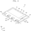
- FIG. 2 is a perspective view illustrating a state in which a display flexible printed circuit board and a touch flexible printed circuit board in the display apparatus of FIG. 1 are bent.
- FIG. 3 is a plan view illustrating a touch screen panel, a display flexible printed circuit board, and a touch flexible printed circuit board, according to an exemplary embodiment of the present inventive concept.
- a display apparatus DP may include a window, which may be referred to herein as a "window member" 100, a touch screen panel 200, a display flexible printed circuit board 300, a touch flexible printed circuit board 400, and a reinforcement member PTL, which may be a supportive structural element, such as a block or rectangular prism (e.g. cuboid).
- FIGS. 1 and 2 illustrate a display apparatus DP which is turned upside down for convenience of description, and the direction in which an image is displayed is a lower direction (a direction opposite to DR3) in the drawings.
- the vertical relationship between elements is determined on the basis of the form in which the display apparatus DP illustrated in FIGS 1 and 2 is turned upside down.
- the window member 100 is disposed on the touch screen panel 200.
- the window member 100 so disposed, may serve to protect the touch screen panel 200 from external impact.
- the window member 100 may have a wider area than that of the touch screen panel 200.
- an active area AA and a non-active area NAA may be defined.
- the active area AA may be configured to display an image and sense the touch input.
- the non-active area NAA is adjacent to the active area AA, and does not display an image and does not sense the touch input.
- all of the pixels of the touch screen panel 200, as well as all of the touch sensing elements of the touch screen panel 200, may be disposed exclusively within the active area AA, and not in the non-active area NAA.
- the touch screen panel 200 may include a first side 201 and a second side 203 which primarily extend in directions different from each other (e.g. the first side 201 and the second side 203 may meet at a right angle).
- the extending direction of the first side 201 of the touch screen panel 200 may be defined as a first direction DR1
- the extending direction of the second side 203 of the touch screen panel 200 may be defined as a second direction DR2
- the thickness direction of the touch screen panel 200 may be defined as a third direction DR3.
- the first side 201 and the second side 203 may be an upper side or a lower side of the side surface of the touch screen panel 200.
- the lower side of the side surface of the touch screen panel 200 is illustrated exemplarily.
- the display flexible printed circuit board 300 may be connected to the touch screen panel 200 and may at least partially overlap the first side 201 of the touch screen panel 200.
- the display flexible printed circuit board 300 may include a flexible wiring substrate 301 and a drive circuit chip 303.
- the drive circuit chip 303 is electrically connected to wirings of the flexible wiring substrate 301.
- a signal output from the drive circuit chip 303 may be applied to pixels of the touch screen panel 200 and a gate drive circuit through the wirings of the flexible wiring substrate 301.
- the display apparatus DP may further include a printed circuit board 350.
- the printed circuit board 350 may be connected to the display flexible printed circuit board 300 and the printed circuit board 350 may receive/transmit signals from/to the drive circuit chip 303.
- the printed circuit board 350 may supply image data, control signals, power supply voltage, etc. to the touch screen panel 200 or the display flexible printed circuit board 300.
- the touch flexible printed circuit board 400 may be connected to the second side 203 of the touch screen panel 200.
- the touch flexible printed circuit board 400 may receive/transmit signals for touch coordinate sensing from/to the touch screen panel 200.
- the touch flexible printed circuit board 400 may include a main portion 410 and branch portions 420.
- the branch portions 420 may protrude from the main portion 410.
- the branch portions 420 may be provided in plurality and each of the plurality of branch portions 420 may be spaced apart from its neighboring branch portions in the second direction DR2.
- Each of the plurality of branch portions 420 may protrude from the same main portion 410.
- the main portion 410 and the branch portions 420 may all together have a single integral shape.
- the branch portions 420 may be connected to the touch screen panel 200.
- a touch drive chip may be mounted on the touch flexible printed circuit board 400, and the signals for touch coordinate sensing may be received/transmitted through the touch drive chip.
- the present invention is not limited thereto, and a separate touch printed circuit board may be attached to the touch flexible printed circuit board 400, and the touch drive chip may be mounted on the touch printed circuit board.
- the reinforcement member PTL may be in contact with both a lower surface of the touch flexible printed circuit board 400 and a portion of the side surface of the touch screen panel 200.
- a first bending area BA1 may be defined in the non-active area NAA of the touch screen panel 200.
- the first bending area BA1 may extend in the first direction DR1 and may be defined between the active area AA and the display flexible printed circuit board 300.
- the touch screen panel 200 may be bent about a first reference axis AX1 extending in the first direction DR1 within the first bending area BA1.
- a second bending area BA2 may be defined in the touch flexible printed circuit board 400.
- the second bending area BA2 may extend in the second direction DR2.
- the touch flexible printed circuit board 400 may be bent about a second reference axis AX2 extending in the second direction DR2 within the second bending area BA2.
- the first bending area BA1 and the second bending area BA2 may each be defined in the window member 100.
- the window member 100 may be exposed through spaces between the branch portions 420.
- the widow member 100 may be supported by a frame disposed between the several branch portions 420.
- the touch screen panel 200 may be divided into a first portion 200-1 and a second portion 200-2.
- the first bending area BA1 may separate the first portion 200-1 from the second portion 200-2.
- both the active area AA and a portion of the non-active area NAA are present, and in the second portion 200-2, only the non-active area is present.
- the second portion 200-2 of the touch screen panel 200 may at least partially overlap the main portion 410 of the touch flexible printed circuit board 400.
- the display flexible printed circuit board and the touch flexible printed circuit board are connected to one side of the touch screen panel.
- the display flexible display circuit board or the touch flexible printed circuit board is bent to the outside of the touch flexible printed circuit board, so that the radius of curvature is increased.
- a size of a bezel may be increased around one side of the touch screen panel.
- the display flexible printed circuit board 300 and the touch flexible printed circuit board 400 are connected to different sides of the touch screen panel 200, so that the radius of curvature of the touch flexible printed circuit board 400 may be minimized, and the bezel of the display apparatus DP may be reduced.
- FIG. 4 is a cross-sectional view illustrating a portion of a touch screen panel.
- one pixel may be disposed in one pixel area PA.
- the touch screen panel 200 may include a display panel 210 and a touch sensing unit 250.
- the display panel 210 may be flexible. According to an exemplary embodiment of the present inventive concept, the display panel 210 will be exemplarily described as an organic light emitting display panel.
- the display panel 210 may include a base substrate 211, a drive layer 213, an organic light emitting device layer 215 and an encapsulation layer 217.
- the base substrate 211 may be a flexible substrate, and may be made of a plastic having excellent heat resistance and durability, such as polyethylene ether phthalate, polyethylene naphthalate, polycarbonate, polyacrylate, polyether imide, polyether sulfone, polyimide, or the like.
- the base substrate 211 will be exemplarily described as a base substrate including polyimide.
- the drive layer 213 may include devices for providing signals to the organic light emitting device layer 215.
- the drive layer 213 may include various signal lines, for example, a scan line, a data line, a power supply line, and a light emitting line.
- the drive layer 213 may include a plurality of transistors and capacitors.
- the transistors may include a switching transistor and a drive transistor Qd.
- the drive transistor Qd is illustrated exemplarily.
- the drive transistor Qd includes an active layer 221, a gate electrode 223, a source electrode 225, and a drain electrode 227.
- the active layer 221 may be disposed on the base substrate 211.
- the drive layer 213 may further include a first insulation layer 231 disposed between the active layer 221 and the gate electrode 223.
- the first insulation layer 231 may insulate the active layer 221 and the gate electrode 223 from each other.
- the source electrode 225 and the drain electrode 227 may each be disposed on the gate electrode 223.
- the drive layer 213 may further include a second insulation layer 233 disposed between the gate electrode 223 and the source electrode 225 and between the gate electrode 223 and the drain electrode 227.
- the source electrode 225 and the drain electrode 227 may be respectively connected to the active layer 221 through contact holes CH1 and CH2 provided in the first insulation layer 231 and the second insulation layer 233.
- the drive layer 213 may further include a protective film 240 disposed on the source electrode 225 and the drain electrode 227.
- the protective film 240 may be planarizing.
- the present invention is not limited to the structure of the drive transistor Qd illustrated in FIG. 4 , and the relative positions and structures of the active layer 221, the gate electrode 223, the source electrode 225 and the drain electrode 227 may be changed into various forms.
- the gate electrode 223 is illustrated as being disposed on the active layer 221 in FIG. 3 , the gate electrode 223 may be disposed under the active layer 221.
- the switching transistor and the drive transistor Qd may have the same structure. However, the present invention is not limited thereto, and the switching transistor and the drive transistor Qd may have different structures. For example, an active layer of the switching transistor and the active layer 221 of the drive transistor Qd may be disposed on different layers.
- the drive layer 213 may further include one or more display pads. Referring back to FIG. 3 , the drive layer 213 may be disposed along the first side 201 of the touch screen panel 200 at a position at least partially overlapping the display flexible printed circuit board 300.
- the organic light emitting device layer 215 may include an organic light emitting diode LD.
- the organic light emitting diode LD is a front light emitting type organic light emitting diode, and it may emit light in the third direction DR3.
- the organic light emitting diode LD may include a first electrode AE, an organic layer OL, and a second electrode CE.
- the first electrode AE is disposed on the protective film 240.
- the first electrode AE is connected to the drain electrode 227 through a contact hole CH3 formed in the protective film 240.
- the first electrode AE may be a pixel electrode or a positive electrode.
- the first electrode AE may be a semi-transmissive electrode or a reflective electrode (i.e. semi-transmissive of light or reflective of light).
- the first electrode AE may include silver (Ag), magnesium (Mg), aluminum (Al), platinum (Pt), palladium (Pd), gold (Au), nickel (Ni), neodymium (Nd), iridium (Ir), chromium (Cr) or a mixture thereof.
- the first electrode AE may be a single layer, or a multilayered structure having a plurality of layers made of a metal oxide or metal.
- the first electrode AE may have, but is not limited to having, a single layer structure made of indium tin oxide (ITO), Ag or a metallic mixture (e.g., a mixture of Ag and Mg), a two-layer structure made of ITO/Mg or ITO/MgF, or a three-layer structure made of ITO/Ag/ITO.
- the organic layer OL may include an organic emission layer EML made of a low-molecular organic material or a polymer organic material.
- the organic emission layer may emit light.
- the organic layer OL may optionally include, in addition to the organic emission layer, a hole transport layer HTL, a hole injection layer HIL, an electron transport layer ETL, an electron injection layer EIL, and the like.
- the second electrode CE may be provided on the organic layer OL.
- the second electrode CE may be a common electrode or a negative electrode.
- the second electrode CE may be a transmissive electrode or a semi-transmissive electrode (i.e. semi-transmissive of light or reflective of light).
- the second electrode CE may include lithium (Li), lithium 8-quinolate (Liq), calcium (Ca), lithium fluoride (LiF)/Ca, LiF/Al, Al, Mg, barium fluoride (BaF), barium (Ba), Ag or a compound or mixture (e.g., a mixture of Ag and Mg) thereof.
- the second electrode CE may include an auxiliary electrode.
- the auxiliary electrode may include a layer formed by depositing the material to face the emission layer, and a transparent metal oxide on the layer, such as indium tin oxide (ITO), indium zinc oxide (IZO), zinc oxide (ZnO) and indium tin zinc oxide (ITZO).
- ITO indium tin oxide
- IZO indium zinc oxide
- ZnO zinc oxide
- ITZO indium tin zinc oxide
- ITZO indium tin zinc oxide
- ITZO indium tin zinc oxide
- ITZO indium tin zinc oxide
- the auxiliary electrode may include molybdenum (Mo), thallium (Ti), Ag, or the like.
- the organic light emitting device layer 215 may further include a pixel definition layer PDL disposed on the protective film 240.
- the pixel definition layer PDL may be disposed so as to at least partially overlap a boundary of the pixel area PA on a plane.
- the encapsulation layer 217 may be disposed on an upper portion of the organic light emitting device layer 215.
- the encapsulation layer 217 may block the penetration of ambient moisture and air into the organic light emitting device layer 215.
- the encapsulation layer 217 may include an encapsulation substrate 241 and a sealing member disposed thereon.
- the sealing member is disposed along an edge of the encapsulation substrate 241, and may seal the organic light emitting diode LD together with the encapsulation substrate 241.
- An interior space 243 formed by the encapsulation substrate 241 and the sealing member may be evacuated.
- the present invention is not limited thereto, and the interior space 243 may be filled with nitrogen (N 2 ), or may be filled with a filling member made of an insulation material.
- the encapsulation layer 217 may include an organic layer and an inorganic layer that are stacked multiple times in the form of a thin film.
- the touch sensing unit 250 may be disposed at an upper portion of the display panel 210.
- the touch sensing unit 250 may be configured to sense the user's touch.
- the touch flexible printed circuit board 400 may be connected to the touch sensing unit 250.
- the touch flexible printed circuit board 400 may provide a touch drive signal to the touch sensing unit 250, and may be configured to sense a touch coordinate from the provided touch drive signal.
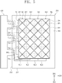
- FIG. 5 is a plan view illustrating the touch sensing unit and the touch flexible printed circuit board of FIG. 4 .
- the touch sensing unit 250 may be realized as a static capacitance type.
- the touch sensing unit 250 may be operated in a way in which touch coordinates are extracted based on capacitance variation amounts of capacitors formed by two kinds of touch lines extending in different directions and insulated and a way in which touch coordinates are extracted based on a capacitance variation amount of capacitors formed by a plurality of touch electrodes disposed in the active area.
- the touch sensing unit 250 will be described in terms of an example operated in the former way.
- the touch sensing unit 250 may be divided into an active area AA1 and a non-active area NAA1.
- the active area AA1 and the non-active area NAA1 of the touch sensing unit 250 may be substantially the same as the active area AA and the non-active area NAA illustrated in FIG 1 , respectively.
- the touch sensing unit 250 may sense a touch input from the active area AA1, and might not sense the touch input from the non-active area NAA1.
- the touch sensing unit 250 may include a base layer TBL, transmission touch lines TX1 to TX5, sensing touch lines RX1 to RX4, transmission lines TL1 to TL5, sensing lines RL1 to RL5, and touch pads TPD.
- Each of the transmission touch lines TX1 to TX5 includes a plurality of transmission touch sensor units SP1 and a plurality of first connection units CP1.
- the transmission touch sensor units SP1 are aligned along the first direction DR1.
- Each of the first connection units CP1 connects two adjacent transmission touch sensor units SP1 among the transmission touch sensor units SP1.
- Each of the transmission touch sensor units SP1 may have a mesh shape having openings disposed therein.
- the sensing touch lines RX1 to RX4 insulate and cross the transmission touch lines TX1 to TX5.
- Each of the sensing touch lines RX1 to RX4 includes a plurality of sensing touch sensor units SP2 and a plurality of second connection units CP2.
- the sensing touch sensor units SP2 are aligned along the second direction DR2.
- Each of the second connection units CP2 connects two adjacent sensing touch sensor units SP2 among the sensing touch sensor units SP2.
- Each of the sensing touch sensor units SP2 may have a mesh shape having various openings disposed therein.
- the transmission touch sensor units SP1 and the first connection units CP1 may be disposed on a first layer, and the sensing touch sensor units SP2 and the second connection units CP2 may be disposed on a second layer different from the first layer.
- the transmission touch sensor units SP1, the first connection units CP1, and the sensing touch sensor units SP2 may be disposed on the first layer, and the second connection units CP2 may be disposed on the second layer different from the first layer.
- the transmission touch lines TX1 to TX5 and the sensing touch lines RX1 to RX4 form a touch capacitor.
- the touch sensing unit 250 may sense a touch input coordinate based on the capacitance variation amount of the touch capacitor.
- each of the transmission lines TL1 to TL5 may be connected to the transmission touch lines TX1 to TX5.
- the other end of each of the transmission lines TL1 to TL5 may be connected to the touch pads TPD.
- the transmission lines TL1 to TL5 may provide the touch drive signals applied from the touch flexible printed circuit board 400 to the transmission touch lines TX1 to TX5 through the touch pads TPD.
- each of the sensing lines RL1 to RL4 may be connected to the sensing touch lines RX1 to RX4.
- the other end of each of the sensing lines RL1 to RL4 may be connected to the touch pads TPD.
- the sensing lines RX1 to RX4 may provide the sensing signals received from the sensing touch lines RX1 to RX4 to the touch flexible printed circuit board 400 through the touch pads TPD.
- the touch sensing unit 250 includes a first side 251 extending in the first direction DR1 and a second side 253 extending in the second direction DR2.
- the first side 251 of the touch sensing unit 250 corresponds to the first side 201 of the touch screen panel 200 described with reference to FIGS. 1 and 2 .
- the second side 253 of the touch sensing unit 250 corresponds to the second side 203 of the touch screen panel 200 described with reference to FIGS. 1 and 2 .
- the touch pads TPD may be disposed along the second side 253 of the touch sensing unit 250.
- FIG. 6 is a cross-sectional view taken along line I-I' of FIG. 3 , in a display apparatus according to an exemplary embodiment of the present inventive concept
- FIG. 7 is a cross-sectional view taken along line II-II' of FIG. 3 , in a display apparatus according to an exemplary embodiment of the present inventive concept.
- the base substrate 211 and the drive layer 213 of the display panel 210 may be bent in the first bending area BA1.
- the touch screen panel 200 may further include a protective film FL disposed on a lower portion of the base substrate 211.
- the protective film FL may protect the base substrate 211.
- the protective film FL may be made of polyethylene terephthalate (PET), polyethylene naphthalate (PEN), polypropylene (PP), polycarbonate (PC), polystyrene (PS), polysulfone (PSul), polyethylene (PE), polyphthalamide (PPA), polyethersulfone (PES), polyarylate (PAR), polycarbonate oxide (PCO), modified polyphenylene oxide (MPPO), or the like.
- the protective film FL is not disposed in the first bending area BA1. Therefore, the base substrate 211 and the drive layer 213 may be easily bent in the first bending area BA1.
- the display panel 210 may further include a stress compensation layer 219.
- the stress compensation layer 219 may be disposed on the drive layer 213 and may cover the first bending area BA1.
- a neutral surface of the display panel 210 may be adjusted in the first bending area BA1 by the stress compensation layer 219. Also, as the base substrate 211 and the drive layer 213 are bent, the tensile stress applied to the base substrate 211 and the drive layer 213 may be mitigated.
- the display apparatus DP may further include a sensor unit SRP.
- the sensor unit SRP may be disposed on the lower portion of the protective film FL.
- the sensor unit SRP may include, but is not limited to including, various sensors such as a force sensor. According to an exemplary embodiment of the present inventive concept, the sensor unit SRP might be omitted.
- the display panel 210 and the touch sensing unit 250 may be attached by a first adhesion layer AD1.
- the first adhesion layer AD1 may be made of a urethane-based material, an acryl-based material, a silicon-based material, or the like.
- the touch sensing unit 250 and the window member 100 may be attached by a second adhesion layer AD2.
- the second adhesion layer AD2 may be made of one of the aforementioned materials and may be made of the same material as the first adhesion layer AD1.
- the touch flexible printed circuit board 400 may be attached to the lower surface of the touch sensing unit 250.
- the reinforcement member PTL may be in contact with the lower surface of the touch flexible printed circuit board 400 and a portion of the side surface of the touch screen panel 200.
- the reinforcement member PTL may be attached to the side surface of the display panel 210 and to the lower surface of the touch flexible printed circuit board 400.
- the reinforcement member PTL may be attached to at least the base substrate 211 and the encapsulation layer 217 of the display panel 210.
- the reinforcement member PRL may be attached to the protective film FL.
- the reinforcement layer PTL may be made of a photocurable material, a thermosetting material, or a natural curable material.
- the reinforcement member PTL is attached to the side surface of the display panel 210, so that cracks may be prevented from occurring in the touch flexible printed circuit board 400.
- FIG. 8 is an enlarged plan view illustrating area BB of FIG. 3 .
- FIG. 8 Only the touch sensing unit 250 of the touch screen panel 200 is illustrated in FIG. 8 . However, it is to be understood that various other components may also be provided.
- the touch pads TPD are disposed along the second side 253 of the touch sensing unit 250.
- the touch flexible printed circuit board 400 and the touch sensing unit 250 may be electrically connected to each other through the touch pads TPD.
- the reinforcement member PTL may be disposed between the second bending area BA2 and the touch sensing unit 250 in the first direction DR1.
- the present invention is not limited to this particular configuration.
- the reinforcement member PTL may be disposed so as to partially overlap the second bending area BA2.
- FIG. 9 is a cross-sectional view taken along line II-II' of FIG. 3 , in a display apparatus according to an exemplary embodiment of the present inventive concept.
- a display apparatus DP1 to be described with reference to FIG. 9 differs from the display apparatus DP described with reference to FIG. 7 in configurations of a touch flexible printed circuit board 401 and a reinforcement member PTL1, and to the extent that details concerning other elements are omitted, it may be assumed that the omitted elements are at least similar to corresponding elements that have already been described.
- the difference between the display apparatus DP1 of FIG. 9 and the display apparatus DP of FIG. 7 will be mainly described.
- the touch flexible printed circuit board 401 of the display apparatus DP1 may be attached to the upper surface of the touch sensing unit 250.
- the reinforcement member PTL1 may be attached to a lower surface of the touch flexible printed circuit board 401, a side surface of the touch sensing unit 250, and a side surface of the display panel 210.
- the reinforcement member PTL1 is attached to the side surface of the touch sensing unit 250, so that the touch flexible printed circuit board 401 may be supported more firmly than in the configuration illustrated in FIG. 7 . Therefore, the reinforcement member PTL1 may prevent cracks from occurring in the touch flexible printed circuit board 401.
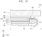
- FIG. 10 is a cross-sectional view taken along line II-II' of FIG. 3 , in a display apparatus according to an exemplary embodiment of the present inventive concept.
- a display apparatus DP2 to be described with reference to FIG. 10 differs from the display apparatus described with reference to FIG. 7 in configuration of a reinforcement member PTL2, and to the extent that details concerning other elements are omitted, it may be assumed that the omitted elements are at least similar to corresponding elements that have already been described.
- the difference between the display apparatus of FIG. 10 and the display apparatus of FIG. 7 will be mainly described.
- the reinforcement member PTL2 of the display apparatus DP2 may be attached to a lower surface of the touch flexible printed circuit board 400 by a third adhesion layer AD3.
- the reinforcement member PTL2 may be in contact with a side surface of the display panel 210.
- the reinforcement member PTL2 is exemplarily illustrated as not being attached to the side surface of the display panel 210.
- the present invention is not limited to this particular configuration, and the reinforcement member PTL2 may be attached to the side surface of the display panel 210 through the adhesion layer. Further, the reinforcement member PTL2 may be attached to the lower surface of the touch flexible printed circuit board 400 or the side surface of the display panel 210.
- the reinforcement member PTL2 may be made of a rubber or urethane-based material.
- the reinforcement member PTL2 may be in contact with the touch flexible printed circuit board 400 in the second bending area BA2 to support the bending of the touch flexible printed circuit board 400.
- the reinforcement member PTL2 may prevent cracks from occurring in the touch flexible printed circuit board 400.
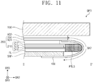
- FIG. 11 is a cross-sectional view taken along line II-II' of FIG. 3 , in a display apparatus according to an exemplary embodiment of the present inventive concept.
- a display apparatus DP3 described with reference to FIG.11 differs from the display apparatus DP described with reference to FIG. 7 in the configuration of a reinforcement member PTL3, and the remaining elements may be assumed to be substantially similar to corresponding elements described in detail above.
- the difference between the display apparatus DP3 of FIG. 11 and the display apparatus DP of FIG. 7 will be mainly described.
- the reinforcement member PTL3 of the display apparatus DP3 may be attached to a side surface of the display panel 210.
- One side of the reinforcement member PTL3 may have a substantially rounded shape.
- One side of the reinforcement member PTL3 may be in contact with the touch flexible printed circuit board 400 in the second bending area BA2 to support the bending of the touch flexible printed circuit board 400.
- the reinforcement member PTL3 may prevent cracks from occurring in the touch flexible printed circuit board 400.
- the radii of curvature of a display flexible printed circuit board and a touch flexible printed circuit board may be minimized, thereby reducing the size of the bezel of the display apparatus.
- a display apparatus having a reinforcement member attached on a lower surface of a touch flexible printed circuit board and a side surface of the touch screen panel, thereby preventing an adhesive portion of a touch flexible printed circuit board from cracking.
Landscapes
- Engineering & Computer Science (AREA)
- Theoretical Computer Science (AREA)
- General Engineering & Computer Science (AREA)
- Physics & Mathematics (AREA)
- General Physics & Mathematics (AREA)
- Human Computer Interaction (AREA)
- Microelectronics & Electronic Packaging (AREA)
- Optics & Photonics (AREA)
- Geometry (AREA)
- Devices For Indicating Variable Information By Combining Individual Elements (AREA)
- Electroluminescent Light Sources (AREA)
Abstract
A display apparatus includes a touch screen panel having an active area and a non-active area. The touch screen panel includes a first side and a second side. A display flexible printed circuit board is connected to the touch screen panel. The display flexible printed circuit board at least partially overlaps the first side of the touch screen panel. A touch flexible printed circuit board is connected to the touch screen panel. The touch flexible printed circuit board at least partially overlaps the second side of the touch screen panel. The touch flexible printed circuit board is bent toward a lower surface of the touch screen panel. A reinforcement member contacts a lower surface of the touch flexible printed circuit board. A portion of a side surface of the touch screen panel is connected to the second side of the touch screen panel.
Description
- The present disclosure relates to a display apparatus, and more particularly, to an organic light emitting diode (OLED) display apparatus with a reduced bezel.
- Organic light emitting diode (OLED) displays represent an important display technology. As with most modern display devices, OLED displays often include a display panel and a touch panel. The display panel includes a plurality of pixels configured to display an image. Each of the plurality of pixels includes an organic light emitting diode (OLED) and a circuit unit configured to control the organic light emitting diode. The circuit unit includes at least a control transistor, a drive transistor, and a storage capacitor. The touch panel may be disposed on the display panel to sense a touch input and calculate touch coordinates therefrom.
- A display circuit board is generally connected to the display panel, and a touch circuit board is generally connected to the touch panel.
- Many modern display panels, such as OLED display devices, are configured to be bent. However, it is possible that in bending these display panels, cracks might occur. These cracks may render the display device inoperable or otherwise defective.
- A display apparatus includes a touch screen panel having an active area and a non-active area defined thereon. The non-active area at least partially surrounds the active area. The touch screen panel includes a first side and a second side. A display flexible printed circuit board is connected to the touch screen panel. The display flexible printed circuit board at least partially overlaps the first side of the touch screen panel. A touch flexible printed circuit board is connected to the touch screen panel. The touch flexible printed circuit board at least partially overlaps the second side of the touch screen panel. The touch flexible printed circuit board is bent toward a lower surface of the touch screen panel. A reinforcement member contacts a lower surface of the touch flexible printed circuit board. A portion of a side surface of the touch screen panel is connected to the second side of the touch screen panel.
- A display apparatus includes a display panel having a first side extending primarily in a first direction. The display panel has an active area and a non-active area defined thereon. The non-active are at least partially surrounds the active area. The display panel is bent with respect to a first reference axis extending in the first direction. A touch sensing unit is disposed on the display panel and has a second side extending in a second direction crossing the first direction. A display flexible printed circuit board is connected to the display panel. The display flexible printed circuit board at least partially overlaps the first side of the display panel. A touch flexible printed circuit board is connected to the touch sensing unit. The touch flexible printed circuit board at least partially overlaps the second side of the touch sensing unit. The touch flexible printed circuit board is bent with respect to a second reference axis extending in the second direction. A reinforcement member contacts both a lower surface of the touch flexible printed circuit board and a portion of a side surface of the display panel.
- A more complete appreciation of the present disclosure and many of the attendant aspects thereof will be readily obtained as the same becomes better understood by reference to the following detailed description when considered in connection with the accompanying drawings, wherein:
-
FIG. 1 is a perspective view illustrating a display apparatus according to an exemplary embodiment of the present inventive concept; -
FIG. 2 is a perspective view illustrating a state in which a display flexible printed circuit board and a touch flexible printed circuit board of the display apparatus ofFIG. 1 are bent; -
FIG. 3 is a plan view illustrating a touch screen panel, a display flexible printed circuit board, and a touch flexible printed circuit board according to an exemplary embodiment of the present inventive concept; -
FIG. 4 is a cross-sectional view illustrating a portion of a touch screen panel; -
FIG. 5 is a plan view illustrating the touch sensing unit and the touch flexible printed circuit board ofFIG. 4 ; -
FIG. 6 is a cross-sectional view taken along line I-I' ofFIG. 3 , in a display apparatus according to an exemplary embodiment of the present inventive concept; -
FIG. 7 is a cross-sectional view taken along line II-II' ofFIG. 3 , in a display apparatus according to an exemplary embodiment of the present inventive concept; -
FIG. 8 is an enlarged plan view illustrating area BB ofFIG. 3 ; -
FIG. 9 is a cross-sectional view taken along line II-II' ofFIG. 3 , in a display apparatus according to an exemplary embodiment of the present inventive concept; -
FIG. 10 is a cross-sectional view taken along line II-II' ofFIG. 3 , in a display apparatus according to an exemplary embodiment of the present inventive concept; and -
FIG.11 is a cross-sectional view taken along line II-II' ofFIG. 3 , in a display apparatus according to an exemplary embodiment of the present inventive concept. - The inventive concept may be modified in many alternate forms, and thus specific embodiments will be exemplified in the drawings and described in detail in the text. It should be understood, however, that the invention is not intended to be limited to the particular forms disclosed.
- In the following description, the terms "upper" and "lower" are used herein to describe the directions based on the drawings. Also, it will be understood that when a portion of a layer, a film, a region, a plate, or the like is referred to as being "on" another portion, it can be "directly on" the other portion, or intervening layers may also be present. Moreover, it will be understood that when a portion such as a layer, a film, an area, a plate, or the like is referred to as being "under" another portion, it can "be directly under" the other portion, or intervening portions may also be present.
-
FIG. 1 is a perspective view illustrating a display apparatus according to an exemplary embodiment of the present inventive concept.FIG. 2 is a perspective view illustrating a state in which a display flexible printed circuit board and a touch flexible printed circuit board in the display apparatus ofFIG. 1 are bent.FIG. 3 . is a plan view illustrating a touch screen panel, a display flexible printed circuit board, and a touch flexible printed circuit board, according to an exemplary embodiment of the present inventive concept. - Referring to
FIGS. 1 to 3 , a display apparatus DP may include a window, which may be referred to herein as a "window member" 100, atouch screen panel 200, a display flexible printedcircuit board 300, a touch flexible printedcircuit board 400, and a reinforcement member PTL, which may be a supportive structural element, such as a block or rectangular prism (e.g. cuboid). -
FIGS. 1 and2 illustrate a display apparatus DP which is turned upside down for convenience of description, and the direction in which an image is displayed is a lower direction (a direction opposite to DR3) in the drawings. In the present specification, the vertical relationship between elements is determined on the basis of the form in which the display apparatus DP illustrated inFIGS 1 and2 is turned upside down. - The
window member 100 is disposed on thetouch screen panel 200. Thewindow member 100, so disposed, may serve to protect thetouch screen panel 200 from external impact. Thewindow member 100 may have a wider area than that of thetouch screen panel 200. - In the
touch screen panel 200, an active area AA and a non-active area NAA may be defined. - The active area AA may be configured to display an image and sense the touch input. The non-active area NAA is adjacent to the active area AA, and does not display an image and does not sense the touch input. Thus, all of the pixels of the
touch screen panel 200, as well as all of the touch sensing elements of thetouch screen panel 200, may be disposed exclusively within the active area AA, and not in the non-active area NAA. - The
touch screen panel 200 may include afirst side 201 and asecond side 203 which primarily extend in directions different from each other (e.g. thefirst side 201 and thesecond side 203 may meet at a right angle). - According to an exemplary embodiment of the present inventive concept, the extending direction of the
first side 201 of thetouch screen panel 200 may be defined as a first direction DR1, the extending direction of thesecond side 203 of thetouch screen panel 200 may be defined as a second direction DR2, and the thickness direction of thetouch screen panel 200 may be defined as a third direction DR3. - When the
touch screen panel 200 is viewed from the third direction DR3, thefirst side 201 and thesecond side 203 may be an upper side or a lower side of the side surface of thetouch screen panel 200. However, inFIGS. 1 and2 , the lower side of the side surface of thetouch screen panel 200 is illustrated exemplarily. - The display flexible printed
circuit board 300 may be connected to thetouch screen panel 200 and may at least partially overlap thefirst side 201 of thetouch screen panel 200. - The display flexible printed
circuit board 300 may include aflexible wiring substrate 301 and adrive circuit chip 303. Thedrive circuit chip 303 is electrically connected to wirings of theflexible wiring substrate 301. A signal output from thedrive circuit chip 303 may be applied to pixels of thetouch screen panel 200 and a gate drive circuit through the wirings of theflexible wiring substrate 301. - The display apparatus DP may further include a printed
circuit board 350. - The printed
circuit board 350 may be connected to the display flexible printedcircuit board 300 and the printedcircuit board 350 may receive/transmit signals from/to thedrive circuit chip 303. The printedcircuit board 350 may supply image data, control signals, power supply voltage, etc. to thetouch screen panel 200 or the display flexible printedcircuit board 300. - The touch flexible printed
circuit board 400 may be connected to thesecond side 203 of thetouch screen panel 200. The touch flexible printedcircuit board 400 may receive/transmit signals for touch coordinate sensing from/to thetouch screen panel 200. - The touch flexible printed
circuit board 400 may include amain portion 410 andbranch portions 420. - The
branch portions 420 may protrude from themain portion 410. Thebranch portions 420 may be provided in plurality and each of the plurality ofbranch portions 420 may be spaced apart from its neighboring branch portions in the second direction DR2. Each of the plurality ofbranch portions 420 may protrude from the samemain portion 410. Themain portion 410 and thebranch portions 420 may all together have a single integral shape. Thebranch portions 420 may be connected to thetouch screen panel 200. - According to an exemplary embodiment of the present inventive concept, a touch drive chip may be mounted on the touch flexible printed
circuit board 400, and the signals for touch coordinate sensing may be received/transmitted through the touch drive chip. However, the present invention is not limited thereto, and a separate touch printed circuit board may be attached to the touch flexible printedcircuit board 400, and the touch drive chip may be mounted on the touch printed circuit board. - The reinforcement member PTL may be in contact with both a lower surface of the touch flexible printed
circuit board 400 and a portion of the side surface of thetouch screen panel 200. - A first bending area BA1 may be defined in the non-active area NAA of the
touch screen panel 200. The first bending area BA1 may extend in the first direction DR1 and may be defined between the active area AA and the display flexible printedcircuit board 300. - The
touch screen panel 200 may be bent about a first reference axis AX1 extending in the first direction DR1 within the first bending area BA1. - A second bending area BA2 may be defined in the touch flexible printed
circuit board 400. The second bending area BA2 may extend in the second direction DR2. The touch flexible printedcircuit board 400 may be bent about a second reference axis AX2 extending in the second direction DR2 within the second bending area BA2. - The first bending area BA1 and the second bending area BA2 may each be defined in the
window member 100. - In a state in which the touch flexible printed
circuit board 400 is bent, thewindow member 100 may be exposed through spaces between thebranch portions 420. Thewidow member 100 may be supported by a frame disposed between theseveral branch portions 420. - The
touch screen panel 200 may be divided into a first portion 200-1 and a second portion 200-2. The first bending area BA1 may separate the first portion 200-1 from the second portion 200-2. In the first portion 200-1, both the active area AA and a portion of the non-active area NAA are present, and in the second portion 200-2, only the non-active area is present. - In a state in which the
touch screen panel 200 and the touch flexible printedcircuit board 400 are bent through the first bending area BA1 and the second bending area BA2, the second portion 200-2 of thetouch screen panel 200 may at least partially overlap themain portion 410 of the touch flexible printedcircuit board 400. - As a comparative example, it may be assumed that the display flexible printed circuit board and the touch flexible printed circuit board are connected to one side of the touch screen panel. In this case, the display flexible display circuit board or the touch flexible printed circuit board is bent to the outside of the touch flexible printed circuit board, so that the radius of curvature is increased. In order to cover the radius of curvature of the touch flexible printed circuit board, a size of a bezel may be increased around one side of the touch screen panel.
- In the display apparatus DP, according to an exemplary embodiment of the present inventive concept, the display flexible printed
circuit board 300 and the touch flexible printedcircuit board 400 are connected to different sides of thetouch screen panel 200, so that the radius of curvature of the touch flexible printedcircuit board 400 may be minimized, and the bezel of the display apparatus DP may be reduced. -
FIG. 4 is a cross-sectional view illustrating a portion of a touch screen panel. InFIG. 4 , one pixel may be disposed in one pixel area PA. - Referring to
FIG. 4 , thetouch screen panel 200 may include adisplay panel 210 and atouch sensing unit 250. - The
display panel 210 may be flexible. According to an exemplary embodiment of the present inventive concept, thedisplay panel 210 will be exemplarily described as an organic light emitting display panel. - The
display panel 210 may include abase substrate 211, adrive layer 213, an organic light emittingdevice layer 215 and anencapsulation layer 217. - The
base substrate 211 may be a flexible substrate, and may be made of a plastic having excellent heat resistance and durability, such as polyethylene ether phthalate, polyethylene naphthalate, polycarbonate, polyacrylate, polyether imide, polyether sulfone, polyimide, or the like. Hereinafter, thebase substrate 211 will be exemplarily described as a base substrate including polyimide. - The
drive layer 213 may include devices for providing signals to the organic light emittingdevice layer 215. Thedrive layer 213 may include various signal lines, for example, a scan line, a data line, a power supply line, and a light emitting line. Thedrive layer 213 may include a plurality of transistors and capacitors. The transistors may include a switching transistor and a drive transistor Qd. - In
FIG. 4 , the drive transistor Qd is illustrated exemplarily. The drive transistor Qd includes anactive layer 221, agate electrode 223, asource electrode 225, and adrain electrode 227. - The
active layer 221 may be disposed on thebase substrate 211. Thedrive layer 213 may further include afirst insulation layer 231 disposed between theactive layer 221 and thegate electrode 223. Thefirst insulation layer 231 may insulate theactive layer 221 and thegate electrode 223 from each other. Thesource electrode 225 and thedrain electrode 227 may each be disposed on thegate electrode 223. Thedrive layer 213 may further include asecond insulation layer 233 disposed between thegate electrode 223 and thesource electrode 225 and between thegate electrode 223 and thedrain electrode 227. Thesource electrode 225 and thedrain electrode 227 may be respectively connected to theactive layer 221 through contact holes CH1 and CH2 provided in thefirst insulation layer 231 and thesecond insulation layer 233. - The
drive layer 213 may further include aprotective film 240 disposed on thesource electrode 225 and thedrain electrode 227. Theprotective film 240 may be planarizing. - The present invention is not limited to the structure of the drive transistor Qd illustrated in
FIG. 4 , and the relative positions and structures of theactive layer 221, thegate electrode 223, thesource electrode 225 and thedrain electrode 227 may be changed into various forms. For example, although thegate electrode 223 is illustrated as being disposed on theactive layer 221 inFIG. 3 , thegate electrode 223 may be disposed under theactive layer 221. - The switching transistor and the drive transistor Qd may have the same structure. However, the present invention is not limited thereto, and the switching transistor and the drive transistor Qd may have different structures. For example, an active layer of the switching transistor and the
active layer 221 of the drive transistor Qd may be disposed on different layers. - The
drive layer 213 may further include one or more display pads. Referring back toFIG. 3 , thedrive layer 213 may be disposed along thefirst side 201 of thetouch screen panel 200 at a position at least partially overlapping the display flexible printedcircuit board 300. - The organic light emitting
device layer 215 may include an organic light emitting diode LD. According to an exemplary embodiment of the present inventive concept, the organic light emitting diode LD is a front light emitting type organic light emitting diode, and it may emit light in the third direction DR3. - The organic light emitting diode LD may include a first electrode AE, an organic layer OL, and a second electrode CE.
- The first electrode AE is disposed on the
protective film 240. The first electrode AE is connected to thedrain electrode 227 through a contact hole CH3 formed in theprotective film 240. - The first electrode AE may be a pixel electrode or a positive electrode. The first electrode AE may be a semi-transmissive electrode or a reflective electrode (i.e. semi-transmissive of light or reflective of light). When the first electrode AE is a semi-transmissive electrode or a reflective electrode, the first electrode AE may include silver (Ag), magnesium (Mg), aluminum (Al), platinum (Pt), palladium (Pd), gold (Au), nickel (Ni), neodymium (Nd), iridium (Ir), chromium (Cr) or a mixture thereof.
- The first electrode AE may be a single layer, or a multilayered structure having a plurality of layers made of a metal oxide or metal. For example, the first electrode AE may have, but is not limited to having, a single layer structure made of indium tin oxide (ITO), Ag or a metallic mixture (e.g., a mixture of Ag and Mg), a two-layer structure made of ITO/Mg or ITO/MgF, or a three-layer structure made of ITO/Ag/ITO.
- The organic layer OL may include an organic emission layer EML made of a low-molecular organic material or a polymer organic material. The organic emission layer may emit light. The organic layer OL may optionally include, in addition to the organic emission layer, a hole transport layer HTL, a hole injection layer HIL, an electron transport layer ETL, an electron injection layer EIL, and the like.
- Holes and electrons are injected into the organic emission layer inside the organic layer OL from the first electrode AE and the second electrode CE, respectively. In the organic emission layer, excitons are formed by combinations of holes and electrons, and thus light is emitted while the excitons relax from the excited state to the ground state.
- The second electrode CE may be provided on the organic layer OL. The second electrode CE may be a common electrode or a negative electrode. The second electrode CE may be a transmissive electrode or a semi-transmissive electrode (i.e. semi-transmissive of light or reflective of light). When the second electrode CE is a transmissive or semi-transmissive electrode, the second electrode CE may include lithium (Li), lithium 8-quinolate (Liq), calcium (Ca), lithium fluoride (LiF)/Ca, LiF/Al, Al, Mg, barium fluoride (BaF), barium (Ba), Ag or a compound or mixture (e.g., a mixture of Ag and Mg) thereof.
- The second electrode CE may include an auxiliary electrode. The auxiliary electrode may include a layer formed by depositing the material to face the emission layer, and a transparent metal oxide on the layer, such as indium tin oxide (ITO), indium zinc oxide (IZO), zinc oxide (ZnO) and indium tin zinc oxide (ITZO). Also, the auxiliary electrode may include molybdenum (Mo), thallium (Ti), Ag, or the like.
- The organic light emitting
device layer 215 may further include a pixel definition layer PDL disposed on theprotective film 240. The pixel definition layer PDL may be disposed so as to at least partially overlap a boundary of the pixel area PA on a plane. - The
encapsulation layer 217 may be disposed on an upper portion of the organic light emittingdevice layer 215. Theencapsulation layer 217 may block the penetration of ambient moisture and air into the organic light emittingdevice layer 215. Theencapsulation layer 217 may include anencapsulation substrate 241 and a sealing member disposed thereon. The sealing member is disposed along an edge of theencapsulation substrate 241, and may seal the organic light emitting diode LD together with theencapsulation substrate 241. Aninterior space 243 formed by theencapsulation substrate 241 and the sealing member may be evacuated. However, the present invention is not limited thereto, and theinterior space 243 may be filled with nitrogen (N2), or may be filled with a filling member made of an insulation material. - Unlike the structure illustrated
FIG. 4 , theencapsulation layer 217 may include an organic layer and an inorganic layer that are stacked multiple times in the form of a thin film. - The
touch sensing unit 250 may be disposed at an upper portion of thedisplay panel 210. Thetouch sensing unit 250 may be configured to sense the user's touch. - The touch flexible printed
circuit board 400 may be connected to thetouch sensing unit 250. The touch flexible printedcircuit board 400 may provide a touch drive signal to thetouch sensing unit 250, and may be configured to sense a touch coordinate from the provided touch drive signal. -
FIG. 5 is a plan view illustrating the touch sensing unit and the touch flexible printed circuit board ofFIG. 4 . - Referring to
FIG. 5 , thetouch sensing unit 250 may be realized as a static capacitance type. Thetouch sensing unit 250 may be operated in a way in which touch coordinates are extracted based on capacitance variation amounts of capacitors formed by two kinds of touch lines extending in different directions and insulated and a way in which touch coordinates are extracted based on a capacitance variation amount of capacitors formed by a plurality of touch electrodes disposed in the active area. In the following description, thetouch sensing unit 250 will be described in terms of an example operated in the former way. - The
touch sensing unit 250 may be divided into an active area AA1 and a non-active area NAA1. The active area AA1 and the non-active area NAA1 of thetouch sensing unit 250 may be substantially the same as the active area AA and the non-active area NAA illustrated inFIG 1 , respectively. Thetouch sensing unit 250 may sense a touch input from the active area AA1, and might not sense the touch input from the non-active area NAA1. - The
touch sensing unit 250 may include a base layer TBL, transmission touch lines TX1 to TX5, sensing touch lines RX1 to RX4, transmission lines TL1 to TL5, sensing lines RL1 to RL5, and touch pads TPD. - Each of the transmission touch lines TX1 to TX5 includes a plurality of transmission touch sensor units SP1 and a plurality of first connection units CP1. The transmission touch sensor units SP1 are aligned along the first direction DR1. Each of the first connection units CP1 connects two adjacent transmission touch sensor units SP1 among the transmission touch sensor units SP1. Each of the transmission touch sensor units SP1 may have a mesh shape having openings disposed therein.
- The sensing touch lines RX1 to RX4 insulate and cross the transmission touch lines TX1 to TX5. Each of the sensing touch lines RX1 to RX4 includes a plurality of sensing touch sensor units SP2 and a plurality of second connection units CP2. The sensing touch sensor units SP2 are aligned along the second direction DR2. Each of the second connection units CP2 connects two adjacent sensing touch sensor units SP2 among the sensing touch sensor units SP2. Each of the sensing touch sensor units SP2 may have a mesh shape having various openings disposed therein.
- According to an exemplary embodiment of the present inventive concept, the transmission touch sensor units SP1 and the first connection units CP1 may be disposed on a first layer, and the sensing touch sensor units SP2 and the second connection units CP2 may be disposed on a second layer different from the first layer. According to an exemplary embodiment of the present inventive concept, the transmission touch sensor units SP1, the first connection units CP1, and the sensing touch sensor units SP2 may be disposed on the first layer, and the second connection units CP2 may be disposed on the second layer different from the first layer.
- The transmission touch lines TX1 to TX5 and the sensing touch lines RX1 to RX4 form a touch capacitor. The
touch sensing unit 250 may sense a touch input coordinate based on the capacitance variation amount of the touch capacitor. - One end of each of the transmission lines TL1 to TL5 may be connected to the transmission touch lines TX1 to TX5. The other end of each of the transmission lines TL1 to TL5 may be connected to the touch pads TPD. The transmission lines TL1 to TL5 may provide the touch drive signals applied from the touch flexible printed
circuit board 400 to the transmission touch lines TX1 to TX5 through the touch pads TPD. - One end of each of the sensing lines RL1 to RL4 may be connected to the sensing touch lines RX1 to RX4. The other end of each of the sensing lines RL1 to RL4 may be connected to the touch pads TPD. The sensing lines RX1 to RX4 may provide the sensing signals received from the sensing touch lines RX1 to RX4 to the touch flexible printed
circuit board 400 through the touch pads TPD. - The
touch sensing unit 250 includes afirst side 251 extending in the first direction DR1 and asecond side 253 extending in the second direction DR2. Thefirst side 251 of thetouch sensing unit 250 corresponds to thefirst side 201 of thetouch screen panel 200 described with reference toFIGS. 1 and2 . Thesecond side 253 of thetouch sensing unit 250 corresponds to thesecond side 203 of thetouch screen panel 200 described with reference toFIGS. 1 and2 . - The touch pads TPD may be disposed along the
second side 253 of thetouch sensing unit 250. -
FIG. 6 is a cross-sectional view taken along line I-I' ofFIG. 3 , in a display apparatus according to an exemplary embodiment of the present inventive concept, andFIG. 7 is a cross-sectional view taken along line II-II' ofFIG. 3 , in a display apparatus according to an exemplary embodiment of the present inventive concept. - Referring to
FIG. 6 , thebase substrate 211 and thedrive layer 213 of thedisplay panel 210 may be bent in the first bending area BA1. - The
touch screen panel 200 may further include a protective film FL disposed on a lower portion of thebase substrate 211. - The protective film FL may protect the
base substrate 211. The protective film FL may be made of polyethylene terephthalate (PET), polyethylene naphthalate (PEN), polypropylene (PP), polycarbonate (PC), polystyrene (PS), polysulfone (PSul), polyethylene (PE), polyphthalamide (PPA), polyethersulfone (PES), polyarylate (PAR), polycarbonate oxide (PCO), modified polyphenylene oxide (MPPO), or the like. - The protective film FL is not disposed in the first bending area BA1. Therefore, the
base substrate 211 and thedrive layer 213 may be easily bent in the first bending area BA1. - The
display panel 210 may further include astress compensation layer 219. Thestress compensation layer 219 may be disposed on thedrive layer 213 and may cover the first bending area BA1. A neutral surface of thedisplay panel 210 may be adjusted in the first bending area BA1 by thestress compensation layer 219. Also, as thebase substrate 211 and thedrive layer 213 are bent, the tensile stress applied to thebase substrate 211 and thedrive layer 213 may be mitigated. - The display apparatus DP may further include a sensor unit SRP. The sensor unit SRP may be disposed on the lower portion of the protective film FL. The sensor unit SRP may include, but is not limited to including, various sensors such as a force sensor. According to an exemplary embodiment of the present inventive concept, the sensor unit SRP might be omitted.
- The
display panel 210 and thetouch sensing unit 250 may be attached by a first adhesion layer AD1. The first adhesion layer AD1 may be made of a urethane-based material, an acryl-based material, a silicon-based material, or the like. - The
touch sensing unit 250 and thewindow member 100 may be attached by a second adhesion layer AD2. The second adhesion layer AD2 may be made of one of the aforementioned materials and may be made of the same material as the first adhesion layer AD1. - Referring to
FIG. 7 , in an exemplary embodiment of the present inventive concept, the touch flexible printedcircuit board 400 may be attached to the lower surface of thetouch sensing unit 250. - The reinforcement member PTL may be in contact with the lower surface of the touch flexible printed
circuit board 400 and a portion of the side surface of thetouch screen panel 200. For example, the reinforcement member PTL may be attached to the side surface of thedisplay panel 210 and to the lower surface of the touch flexible printedcircuit board 400. In this case, the reinforcement member PTL may be attached to at least thebase substrate 211 and theencapsulation layer 217 of thedisplay panel 210. The reinforcement member PRL may be attached to the protective film FL. - The reinforcement layer PTL may be made of a photocurable material, a thermosetting material, or a natural curable material.
- As the touch flexible printed
circuit board 400 is bent, cracks may occur in the vicinity of the adhesion portion between the touch flexible printedcircuit board 400 and thetouch sensing unit 250. The reinforcement member PTL is attached to the side surface of thedisplay panel 210, so that cracks may be prevented from occurring in the touch flexible printedcircuit board 400. -
FIG. 8 is an enlarged plan view illustrating area BB ofFIG. 3 . - Only the
touch sensing unit 250 of thetouch screen panel 200 is illustrated inFIG. 8 . However, it is to be understood that various other components may also be provided. - The touch pads TPD are disposed along the
second side 253 of thetouch sensing unit 250. The touch flexible printedcircuit board 400 and thetouch sensing unit 250 may be electrically connected to each other through the touch pads TPD. - The reinforcement member PTL may be disposed between the second bending area BA2 and the
touch sensing unit 250 in the first direction DR1. However, the present invention is not limited to this particular configuration. For example, the reinforcement member PTL may be disposed so as to partially overlap the second bending area BA2. -
FIG. 9 is a cross-sectional view taken along line II-II' ofFIG. 3 , in a display apparatus according to an exemplary embodiment of the present inventive concept. - A display apparatus DP1 to be described with reference to
FIG. 9 differs from the display apparatus DP described with reference toFIG. 7 in configurations of a touch flexible printedcircuit board 401 and a reinforcement member PTL1, and to the extent that details concerning other elements are omitted, it may be assumed that the omitted elements are at least similar to corresponding elements that have already been described. Hereinafter, the difference between the display apparatus DP1 ofFIG. 9 and the display apparatus DP ofFIG. 7 will be mainly described. - The touch flexible printed
circuit board 401 of the display apparatus DP1 may be attached to the upper surface of thetouch sensing unit 250. - The reinforcement member PTL1 may be attached to a lower surface of the touch flexible printed
circuit board 401, a side surface of thetouch sensing unit 250, and a side surface of thedisplay panel 210. - As the touch flexible printed
circuit board 401 is attached to the upper surface of thetouch sensing unit 250, the reinforcement member PTL1 is attached to the side surface of thetouch sensing unit 250, so that the touch flexible printedcircuit board 401 may be supported more firmly than in the configuration illustrated inFIG. 7 . Therefore, the reinforcement member PTL1 may prevent cracks from occurring in the touch flexible printedcircuit board 401. -
FIG. 10 is a cross-sectional view taken along line II-II' ofFIG. 3 , in a display apparatus according to an exemplary embodiment of the present inventive concept. - A display apparatus DP2 to be described with reference to
FIG. 10 differs from the display apparatus described with reference toFIG. 7 in configuration of a reinforcement member PTL2, and to the extent that details concerning other elements are omitted, it may be assumed that the omitted elements are at least similar to corresponding elements that have already been described. Hereinafter, the difference between the display apparatus ofFIG. 10 and the display apparatus ofFIG. 7 will be mainly described. - The reinforcement member PTL2 of the display apparatus DP2 may be attached to a lower surface of the touch flexible printed
circuit board 400 by a third adhesion layer AD3. The reinforcement member PTL2 may be in contact with a side surface of thedisplay panel 210. InFIG. 10 , the reinforcement member PTL2 is exemplarily illustrated as not being attached to the side surface of thedisplay panel 210. However, the present invention is not limited to this particular configuration, and the reinforcement member PTL2 may be attached to the side surface of thedisplay panel 210 through the adhesion layer. Further, the reinforcement member PTL2 may be attached to the lower surface of the touch flexible printedcircuit board 400 or the side surface of thedisplay panel 210. - The reinforcement member PTL2 may be made of a rubber or urethane-based material.
- The reinforcement member PTL2 may be in contact with the touch flexible printed
circuit board 400 in the second bending area BA2 to support the bending of the touch flexible printedcircuit board 400. The reinforcement member PTL2 may prevent cracks from occurring in the touch flexible printedcircuit board 400. -
FIG. 11 is a cross-sectional view taken along line II-II' ofFIG. 3 , in a display apparatus according to an exemplary embodiment of the present inventive concept. - A display apparatus DP3 described with reference to
FIG.11 differs from the display apparatus DP described with reference toFIG. 7 in the configuration of a reinforcement member PTL3, and the remaining elements may be assumed to be substantially similar to corresponding elements described in detail above. Hereinafter, the difference between the display apparatus DP3 ofFIG. 11 and the display apparatus DP ofFIG. 7 will be mainly described. - The reinforcement member PTL3 of the display apparatus DP3 may be attached to a side surface of the
display panel 210. One side of the reinforcement member PTL3 may have a substantially rounded shape. One side of the reinforcement member PTL3 may be in contact with the touch flexible printedcircuit board 400 in the second bending area BA2 to support the bending of the touch flexible printedcircuit board 400. The reinforcement member PTL3 may prevent cracks from occurring in the touch flexible printedcircuit board 400. - In a display apparatus according to an exemplary embodiment of the present inventive concept, the radii of curvature of a display flexible printed circuit board and a touch flexible printed circuit board may be minimized, thereby reducing the size of the bezel of the display apparatus.
- According to an exemplary embodiment of the present inventive concept, there is also provided a display apparatus having a reinforcement member attached on a lower surface of a touch flexible printed circuit board and a side surface of the touch screen panel, thereby preventing an adhesive portion of a touch flexible printed circuit board from cracking.
- Although exemplary embodiments of the present invention have been described, it is understood that the present invention should not be limited to these exemplary embodiments..
- It is clear for a person skilled in the art that the disclosed embodiments can also be combined where possible.
Claims (15)
- A display apparatus, comprising:a touch screen panel (200) having an active area (AA) and a non-active area (NAA) defined thereon, the non-active area (NAA) at least partially surrounding the active area (AA), and the touch screen panel (200) including a first side (201) and a second side (203);a display flexible printed circuit board (300) connected to the touch screen panel (200), the display flexible printed circuit board (300) at least partially overlapping the first side (201) of the touch screen panel (200);a touch flexible printed circuit board (400) connected to the touch screen panel, the touch flexible printed circuit board (400) at least partially overlapping the second side (203) of the touch screen panel (200), and the touch flexible printed circuit board (400) being bent toward a lower surface of the touch screen panel (200); anda reinforcement member (PTL) contacting a lower surface of the touch flexible printed circuit board (400) and a portion of a side surface of the touch screen panel (200) connected to the second side (203) of the touch screen panel (200).
- The display apparatus of claim 1, wherein the touch screen panel (200), comprises:a display panel (210); anda touch sensing unit (250) disposed on the display panel (210),wherein the display flexible printed circuit board (300) is attached to an upper surface of the display panel (210), andwherein the touch flexible printed circuit board (400) is attached to the touch sensing unit (250).
- The display apparatus of claim 2, wherein the touch flexible printed circuit board (400) is attached to a lower surface of the touch sensing unit (250), and
wherein the reinforcement member (PTL) is attached to both a side surface of the display panel (210) and the lower surface of the touch flexible printed circuit board (400). - The display apparatus of claim 2, wherein the touch flexible printed circuit board (400) is attached to an upper surface of the touch sensing unit (250), and
wherein the reinforcement member (PTL) is attached to both a side surface of the display panel (210) and a side surface of the touch sensing unit (250). - The display apparatus of one of the preceding claims, wherein the reinforcement member (PTL) comprises a curable material.
- The display apparatus of one of the preceding claims, wherein the non-active area (NAA) of the touch screen panel (200) includes a first bending area (BA1) extending in a direction parallel to the first side (201) of the touch screen panel (200),
wherein the first bending area is defined between the active area (AA) and the display flexible printed circuit board (300), and
wherein the touch screen panel (200) is configured to be bent in the first bending area (BA1). - The display apparatus of claim 6, wherein the touch screen panel (200) further comprises a protective film disposed under the display panel (210), and
wherein the protective film does not overlap the first bending area (BA1). - The display apparatus of one of claims 2 to 7, wherein the display panel (210) comprises:a base substrate (211);a drive layer (213) disposed on the base substrate and including a plurality of signal lines and a transistor;an organic light emitting device layer (215) configured to receive signals from the drive layer and including an organic light emitting diode disposed within the active area;a stress compensation layer (219) disposed on the drive layer (213) and configured to at least partially cover the first bending area (BA1); andan encapsulation layer (217) covering the organic light emitting device layer.
- The display apparatus of one of the preceding claims, wherein the touch flexible printed circuit board (400) includes a second bending area (BA2) extending in a direction parallel to the second side (203) of the touch screen panel (200), and
wherein the touch flexible printed circuit board (400) is configured to be bent in the second bending area (BA2). - The display apparatus of claim 9, wherein the touch screen panel (200) comprises a first portion (200-1) and a second potion (200-2) separated from each other by the first bending area (BA1), and wherein the active area (AA) is defined within the first portion (200-1), and
wherein the second portion (200-2) of the touch screen panel (200) at least partially overlaps the touch flexible printed circuit board (400) in a state in which both the touch screen panel (200) and the touch flexible printed circuit board (400) are bent. - The display apparatus of claim 9 or 10, wherein the reinforcement member (PTL) is attached to a lower surface of the touch flexible printed circuit board (400) and/or a side surface of the display panel (210), and
wherein the reinforcement member (PTL) is in contact with the touch flexible printed circuit board (400) in the second bending area. - The display apparatus of claim 11, wherein the reinforcement member (PTL) includes a rubber or a urethane-based material.
- The display apparatus of claim 9, wherein the reinforcement member (PTL) is attached to a side surface of the display panel (210), and
wherein one side of the reinforcement member (PTL) has a rounded shape and is in contact with the touch flexible printed circuit board in the second bending area. - The display apparatus of one of claims 2 to 13, wherein the touch flexible printed circuit board (400) comprises a main portion (410) and a plurality of branch portions (420), each of which protrudes from the main portion (410), wherein each of the plurality of branch portions (420) is attached to the touch sensing unit (250), and each of the plurality of branch portions (420) is spaced apart from neighboring branch portions of the plurality of branch portions (420).
- The display apparatus of claim 14, wherein the plurality of branch portions (420) includes a second bending area extending in a direction parallel to the second side (203), wherein each of the plurality of branch portions is configured to be bent in the second bending area.
Applications Claiming Priority (1)
| Application Number | Priority Date | Filing Date | Title |
|---|---|---|---|
| KR1020180020720A KR102502274B1 (en) | 2018-02-21 | 2018-02-21 | Display apparatus |
Publications (1)
| Publication Number | Publication Date |
|---|---|
| EP3531256A1 true EP3531256A1 (en) | 2019-08-28 |
Family
ID=65520113
Family Applications (1)
| Application Number | Title | Priority Date | Filing Date |
|---|---|---|---|
| EP19158481.2A Withdrawn EP3531256A1 (en) | 2018-02-21 | 2019-02-21 | Oled display apparatus |
Country Status (6)
| Country | Link |
|---|---|
| US (1) | US10811471B2 (en) |
| EP (1) | EP3531256A1 (en) |
| JP (1) | JP7353769B2 (en) |
| KR (1) | KR102502274B1 (en) |
| CN (1) | CN110176475B (en) |
| TW (1) | TWI830719B (en) |
Families Citing this family (28)
| Publication number | Priority date | Publication date | Assignee | Title |
|---|---|---|---|---|
| KR102621685B1 (en) * | 2018-09-18 | 2024-01-09 | 삼성디스플레이 주식회사 | Touch screen and display device having the same |
| KR102205125B1 (en) * | 2019-09-17 | 2021-01-19 | 연세대학교 산학협력단 | Apparatus for Printing Wires of Bezel-Less Display, and Display |
| JP7338375B2 (en) * | 2019-09-30 | 2023-09-05 | セイコーエプソン株式会社 | Display device with capacitive touch panel |
| CN112652240A (en) * | 2019-10-11 | 2021-04-13 | 群创光电股份有限公司 | Flexible display device and method for manufacturing flexible display device |
| CN112735261A (en) * | 2019-10-28 | 2021-04-30 | 华为技术有限公司 | Flexible display screen and display terminal |
| KR102760149B1 (en) * | 2019-11-04 | 2025-01-31 | 삼성디스플레이 주식회사 | Display device |
| US12058925B2 (en) * | 2019-11-28 | 2024-08-06 | Chengdu Boe Optoelectronics Technology Co., Ltd. | Display assembly and manufacturing method thereof and display device |
| KR102768125B1 (en) * | 2019-12-02 | 2025-02-13 | 엘지디스플레이 주식회사 | Stretchable display device comprising the same |
| CN111142712B (en) * | 2019-12-31 | 2023-07-18 | 信利(惠州)智能显示有限公司 | Flexible circuit board, display module and display screen |
| KR102874594B1 (en) * | 2019-12-31 | 2025-10-22 | 엘지디스플레이 주식회사 | Display device |
| CN111292622B (en) * | 2020-02-26 | 2022-01-25 | 云谷(固安)科技有限公司 | Display panel and display device |
| CN111508356A (en) * | 2020-04-17 | 2020-08-07 | 武汉华星光电半导体显示技术有限公司 | Display device and electronic equipment |
| CN111524940B (en) * | 2020-04-26 | 2024-07-12 | 武汉华星光电半导体显示技术有限公司 | OLED display screen and preparation method thereof |
| CN113589964A (en) * | 2020-04-30 | 2021-11-02 | 京东方科技集团股份有限公司 | Binding circuit board, display device and electrical equipment |
| CN119861839A (en) * | 2020-05-22 | 2025-04-22 | 宸美(厦门)光电有限公司 | Foldable touch display device |
| CN112102723A (en) * | 2020-09-15 | 2020-12-18 | 京东方科技集团股份有限公司 | Display module, manufacturing method thereof and display device |
| KR20220046750A (en) * | 2020-10-07 | 2022-04-15 | 삼성디스플레이 주식회사 | Display device |
| KR102866444B1 (en) * | 2020-12-21 | 2025-10-01 | 삼성디스플레이 주식회사 | Electronic device |
| KR20220096896A (en) * | 2020-12-31 | 2022-07-07 | 엘지디스플레이 주식회사 | Transparent Touch Display apparatus |
| CN112786557B (en) * | 2021-01-12 | 2023-10-31 | 武汉华星光电半导体显示技术有限公司 | Flexible display devices and terminal equipment |
| CN112929799B (en) * | 2021-01-20 | 2022-11-01 | 武汉华星光电半导体显示技术有限公司 | Vibration sounding assembly and display device |
| US12213260B2 (en) * | 2021-02-25 | 2025-01-28 | Apple Inc. | Electronic device |
| US12003019B2 (en) | 2021-02-25 | 2024-06-04 | Apple Inc. | Electronic device |
| KR20220129123A (en) * | 2021-03-15 | 2022-09-23 | 삼성디스플레이 주식회사 | display device |
| CN114067683B (en) * | 2021-10-18 | 2023-11-24 | 维信诺科技股份有限公司 | Display panels and display devices |
| KR102873685B1 (en) | 2021-11-15 | 2025-10-17 | 엘지디스플레이 주식회사 | Display apparatus |
| KR20230134011A (en) | 2022-03-10 | 2023-09-20 | 삼성디스플레이 주식회사 | Display device and method of operation thereof |
| US20250204214A1 (en) * | 2022-05-18 | 2025-06-19 | Sharp Display Technology Corporation | Display device and method for manufacturing same |
Citations (8)
| Publication number | Priority date | Publication date | Assignee | Title |
|---|---|---|---|---|
| WO2014119972A1 (en) * | 2013-02-01 | 2014-08-07 | LG Display Co.,Ltd. | Electronic devices with flexible display and method for manufacturing the same |
| US20160073528A1 (en) * | 2014-09-04 | 2016-03-10 | Samsung Display Co., Ltd. | Display device |
| US20160147361A1 (en) * | 2014-11-21 | 2016-05-26 | Samsung Display Co., Ltd. | Display device including touch screen panel |
| WO2016111895A1 (en) * | 2015-01-09 | 2016-07-14 | Apple Inc. | Organic light-emitting diode display with bent substrate |
| US20160363800A1 (en) * | 2015-06-09 | 2016-12-15 | Samsung Display Co., Ltd. | Display device |
| EP3139207A1 (en) * | 2015-08-31 | 2017-03-08 | LG Display Co., Ltd. | Back cover and transparent display apparatus including the same |
| US20170194411A1 (en) * | 2015-12-31 | 2017-07-06 | Lg Display Co., Ltd. | Electronic device with flexible display panel |
| US20180027673A1 (en) * | 2016-07-21 | 2018-01-25 | Japan Display Inc. | Method for manufacturing display device and display device |
Family Cites Families (14)
| Publication number | Priority date | Publication date | Assignee | Title |
|---|---|---|---|---|
| JP4582169B2 (en) * | 2008-03-26 | 2010-11-17 | ソニー株式会社 | Capacitance type input device, display device with input function, and electronic device |
| KR101870798B1 (en) | 2011-08-30 | 2018-06-26 | 엘지디스플레이 주식회사 | Flexible display device and method for manufacturing the same |
| KR20130027307A (en) * | 2011-09-07 | 2013-03-15 | 삼성전기주식회사 | Touch pannel |
| US9083344B2 (en) * | 2012-02-01 | 2015-07-14 | Apple Inc. | Touch sensor with integrated signal bus extensions |
| KR102178470B1 (en) * | 2012-09-26 | 2020-11-18 | 엘지디스플레이 주식회사 | Display device having a flexible film cable |
| KR102095013B1 (en) * | 2013-04-11 | 2020-03-31 | 삼성디스플레이 주식회사 | Flexible device |
| JP6142745B2 (en) * | 2013-09-10 | 2017-06-07 | ソニー株式会社 | Sensor device, input device and electronic apparatus |
| KR102168132B1 (en) * | 2013-12-31 | 2020-10-21 | 삼성디스플레이 주식회사 | Organic light emitting device |
| US9706607B2 (en) * | 2014-12-10 | 2017-07-11 | Lg Display Co., Ltd. | Flexible display device with multiple types of micro-coating layers |
| US9780157B2 (en) | 2014-12-23 | 2017-10-03 | Lg Display Co., Ltd. | Flexible display device with gate-in-panel circuit |
| KR102275318B1 (en) | 2015-03-02 | 2021-07-13 | 삼성디스플레이 주식회사 | Image display apparatus |
| KR102577239B1 (en) * | 2015-12-16 | 2023-09-08 | 엘지디스플레이 주식회사 | Flexible display apparatus |
| JP6695727B2 (en) * | 2016-04-08 | 2020-05-20 | 株式会社ジャパンディスプレイ | Display device |
| EP3293606B1 (en) * | 2016-09-09 | 2020-12-30 | Samsung Display Co., Ltd. | Display device and method of manufacturing electronic device using the same |
-
2018
- 2018-02-21 KR KR1020180020720A patent/KR102502274B1/en active Active
-
2019
- 2019-02-07 US US16/270,130 patent/US10811471B2/en active Active
- 2019-02-20 CN CN201910125564.0A patent/CN110176475B/en active Active
- 2019-02-21 JP JP2019029262A patent/JP7353769B2/en active Active
- 2019-02-21 EP EP19158481.2A patent/EP3531256A1/en not_active Withdrawn
- 2019-02-21 TW TW108105881A patent/TWI830719B/en active
Patent Citations (8)
| Publication number | Priority date | Publication date | Assignee | Title |
|---|---|---|---|---|
| WO2014119972A1 (en) * | 2013-02-01 | 2014-08-07 | LG Display Co.,Ltd. | Electronic devices with flexible display and method for manufacturing the same |
| US20160073528A1 (en) * | 2014-09-04 | 2016-03-10 | Samsung Display Co., Ltd. | Display device |
| US20160147361A1 (en) * | 2014-11-21 | 2016-05-26 | Samsung Display Co., Ltd. | Display device including touch screen panel |
| WO2016111895A1 (en) * | 2015-01-09 | 2016-07-14 | Apple Inc. | Organic light-emitting diode display with bent substrate |
| US20160363800A1 (en) * | 2015-06-09 | 2016-12-15 | Samsung Display Co., Ltd. | Display device |
| EP3139207A1 (en) * | 2015-08-31 | 2017-03-08 | LG Display Co., Ltd. | Back cover and transparent display apparatus including the same |
| US20170194411A1 (en) * | 2015-12-31 | 2017-07-06 | Lg Display Co., Ltd. | Electronic device with flexible display panel |
| US20180027673A1 (en) * | 2016-07-21 | 2018-01-25 | Japan Display Inc. | Method for manufacturing display device and display device |
Also Published As
| Publication number | Publication date |
|---|---|
| US20190259818A1 (en) | 2019-08-22 |
| JP2019144551A (en) | 2019-08-29 |
| KR102502274B1 (en) | 2023-02-22 |
| TW201941037A (en) | 2019-10-16 |
| CN110176475A (en) | 2019-08-27 |
| KR20190100997A (en) | 2019-08-30 |
| JP7353769B2 (en) | 2023-10-02 |
| US10811471B2 (en) | 2020-10-20 |
| TWI830719B (en) | 2024-02-01 |
| CN110176475B (en) | 2024-06-14 |
Similar Documents
| Publication | Publication Date | Title |
|---|---|---|
| EP3531256A1 (en) | Oled display apparatus | |
| US11249588B2 (en) | Display apparatus | |
| US10347866B1 (en) | Organic light emitting display apparatus having an insulating dam | |
| JP7002908B2 (en) | Display device | |
| JP6706999B2 (en) | Display device | |
| KR102111562B1 (en) | Thin film semiconductor device and organic light emitting display | |
| US9989820B2 (en) | Display device including flexible printed circuit board | |
| US9412803B2 (en) | Display device | |
| JP6785627B2 (en) | Display device | |
| US11107416B2 (en) | Display device | |
| US20150090969A1 (en) | Display device | |
| KR102891653B1 (en) | Touch display device | |
| KR20180047536A (en) | Organic light emitting display device | |
| KR20180028597A (en) | Display device | |
| KR20180073352A (en) | Organic light emitting display device | |
| KR20160000980A (en) | Organic light emitting display device | |
| KR20210084990A (en) | Display device | |
| US9263474B2 (en) | Thin film transistor array substrate and organic light-emitting display apparatus including the same | |
| KR102911310B1 (en) | Organic light emitting display device | |
| KR20190049173A (en) | Display device | |
| KR101950472B1 (en) | Flexible display apparatus and the method of manufacturing the same | |
| KR20210058333A (en) | Display device | |
| US20250127019A1 (en) | Display device | |
| KR20220133828A (en) | Flexible display apparatus and the method of manufacturing the same | |
| CN121646145A (en) | Display device and manufacturing method thereof |
Legal Events
| Date | Code | Title | Description |
|---|---|---|---|
| PUAI | Public reference made under article 153(3) epc to a published international application that has entered the european phase |
Free format text: ORIGINAL CODE: 0009012 |
|
| STAA | Information on the status of an ep patent application or granted ep patent |
Free format text: STATUS: THE APPLICATION HAS BEEN PUBLISHED |
|
| AK | Designated contracting states |
Kind code of ref document: A1 Designated state(s): AL AT BE BG CH CY CZ DE DK EE ES FI FR GB GR HR HU IE IS IT LI LT LU LV MC MK MT NL NO PL PT RO RS SE SI SK SM TR |
|
| AX | Request for extension of the european patent |
Extension state: BA ME |
|
| STAA | Information on the status of an ep patent application or granted ep patent |
Free format text: STATUS: THE APPLICATION IS DEEMED TO BE WITHDRAWN |
|
| 18D | Application deemed to be withdrawn |
Effective date: 20200229 |