EP3529922B1 - A current modulation circuit, a driving circuit, and a method for driving a lighting load with current modulation - Google Patents
A current modulation circuit, a driving circuit, and a method for driving a lighting load with current modulation Download PDFInfo
- Publication number
- EP3529922B1 EP3529922B1 EP17780138.8A EP17780138A EP3529922B1 EP 3529922 B1 EP3529922 B1 EP 3529922B1 EP 17780138 A EP17780138 A EP 17780138A EP 3529922 B1 EP3529922 B1 EP 3529922B1
- Authority
- EP
- European Patent Office
- Prior art keywords
- current
- voltage
- circuit
- modulating element
- pass filter
- Prior art date
- Legal status (The legal status is an assumption and is not a legal conclusion. Google has not performed a legal analysis and makes no representation as to the accuracy of the status listed.)
- Active
Links
Images


Classifications
-
- H—ELECTRICITY
- H04—ELECTRIC COMMUNICATION TECHNIQUE
- H04B—TRANSMISSION
- H04B10/00—Transmission systems employing electromagnetic waves other than radio-waves, e.g. infrared, visible or ultraviolet light, or employing corpuscular radiation, e.g. quantum communication
- H04B10/11—Arrangements specific to free-space transmission, i.e. transmission through air or vacuum
- H04B10/114—Indoor or close-range type systems
- H04B10/116—Visible light communication
-
- H—ELECTRICITY
- H02—GENERATION; CONVERSION OR DISTRIBUTION OF ELECTRIC POWER
- H02M—APPARATUS FOR CONVERSION BETWEEN AC AND AC, BETWEEN AC AND DC, OR BETWEEN DC AND DC, AND FOR USE WITH MAINS OR SIMILAR POWER SUPPLY SYSTEMS; CONVERSION OF DC OR AC INPUT POWER INTO SURGE OUTPUT POWER; CONTROL OR REGULATION THEREOF
- H02M1/00—Details of apparatus for conversion
- H02M1/08—Circuits specially adapted for the generation of control voltages for semiconductor devices incorporated in static converters
-
- H—ELECTRICITY
- H02—GENERATION; CONVERSION OR DISTRIBUTION OF ELECTRIC POWER
- H02M—APPARATUS FOR CONVERSION BETWEEN AC AND AC, BETWEEN AC AND DC, OR BETWEEN DC AND DC, AND FOR USE WITH MAINS OR SIMILAR POWER SUPPLY SYSTEMS; CONVERSION OF DC OR AC INPUT POWER INTO SURGE OUTPUT POWER; CONTROL OR REGULATION THEREOF
- H02M1/00—Details of apparatus for conversion
- H02M1/14—Arrangements for reducing ripples from DC input or output
-
- H—ELECTRICITY
- H05—ELECTRIC TECHNIQUES NOT OTHERWISE PROVIDED FOR
- H05B—ELECTRIC HEATING; ELECTRIC LIGHT SOURCES NOT OTHERWISE PROVIDED FOR; CIRCUIT ARRANGEMENTS FOR ELECTRIC LIGHT SOURCES, IN GENERAL
- H05B45/00—Circuit arrangements for operating light-emitting diodes [LED]
- H05B45/30—Driver circuits
- H05B45/347—Dynamic headroom control [DHC]
-
- H—ELECTRICITY
- H05—ELECTRIC TECHNIQUES NOT OTHERWISE PROVIDED FOR
- H05B—ELECTRIC HEATING; ELECTRIC LIGHT SOURCES NOT OTHERWISE PROVIDED FOR; CIRCUIT ARRANGEMENTS FOR ELECTRIC LIGHT SOURCES, IN GENERAL
- H05B45/00—Circuit arrangements for operating light-emitting diodes [LED]
- H05B45/30—Driver circuits
- H05B45/395—Linear regulators
-
- H—ELECTRICITY
- H05—ELECTRIC TECHNIQUES NOT OTHERWISE PROVIDED FOR
- H05B—ELECTRIC HEATING; ELECTRIC LIGHT SOURCES NOT OTHERWISE PROVIDED FOR; CIRCUIT ARRANGEMENTS FOR ELECTRIC LIGHT SOURCES, IN GENERAL
- H05B47/00—Circuit arrangements for operating light sources in general, i.e. where the type of light source is not relevant
- H05B47/10—Controlling the light source
- H05B47/105—Controlling the light source in response to determined parameters
- H05B47/11—Controlling the light source in response to determined parameters by determining the brightness or colour temperature of ambient light
-
- H—ELECTRICITY
- H05—ELECTRIC TECHNIQUES NOT OTHERWISE PROVIDED FOR
- H05B—ELECTRIC HEATING; ELECTRIC LIGHT SOURCES NOT OTHERWISE PROVIDED FOR; CIRCUIT ARRANGEMENTS FOR ELECTRIC LIGHT SOURCES, IN GENERAL
- H05B47/00—Circuit arrangements for operating light sources in general, i.e. where the type of light source is not relevant
- H05B47/10—Controlling the light source
- H05B47/175—Controlling the light source by remote control
- H05B47/185—Controlling the light source by remote control via power line carrier transmission
-
- H—ELECTRICITY
- H05—ELECTRIC TECHNIQUES NOT OTHERWISE PROVIDED FOR
- H05B—ELECTRIC HEATING; ELECTRIC LIGHT SOURCES NOT OTHERWISE PROVIDED FOR; CIRCUIT ARRANGEMENTS FOR ELECTRIC LIGHT SOURCES, IN GENERAL
- H05B45/00—Circuit arrangements for operating light-emitting diodes [LED]
- H05B45/30—Driver circuits
- H05B45/37—Converter circuits
- H05B45/3725—Switched mode power supply [SMPS]
-
- Y—GENERAL TAGGING OF NEW TECHNOLOGICAL DEVELOPMENTS; GENERAL TAGGING OF CROSS-SECTIONAL TECHNOLOGIES SPANNING OVER SEVERAL SECTIONS OF THE IPC; TECHNICAL SUBJECTS COVERED BY FORMER USPC CROSS-REFERENCE ART COLLECTIONS [XRACs] AND DIGESTS
- Y02—TECHNOLOGIES OR APPLICATIONS FOR MITIGATION OR ADAPTATION AGAINST CLIMATE CHANGE
- Y02B—CLIMATE CHANGE MITIGATION TECHNOLOGIES RELATED TO BUILDINGS, e.g. HOUSING, HOUSE APPLIANCES OR RELATED END-USER APPLICATIONS
- Y02B20/00—Energy efficient lighting technologies, e.g. halogen lamps or gas discharge lamps
- Y02B20/30—Semiconductor lamps, e.g. solid state lamps [SSL] light emitting diodes [LED] or organic LED [OLED]
-
- Y—GENERAL TAGGING OF NEW TECHNOLOGICAL DEVELOPMENTS; GENERAL TAGGING OF CROSS-SECTIONAL TECHNOLOGIES SPANNING OVER SEVERAL SECTIONS OF THE IPC; TECHNICAL SUBJECTS COVERED BY FORMER USPC CROSS-REFERENCE ART COLLECTIONS [XRACs] AND DIGESTS
- Y02—TECHNOLOGIES OR APPLICATIONS FOR MITIGATION OR ADAPTATION AGAINST CLIMATE CHANGE
- Y02B—CLIMATE CHANGE MITIGATION TECHNOLOGIES RELATED TO BUILDINGS, e.g. HOUSING, HOUSE APPLIANCES OR RELATED END-USER APPLICATIONS
- Y02B20/00—Energy efficient lighting technologies, e.g. halogen lamps or gas discharge lamps
- Y02B20/40—Control techniques providing energy savings, e.g. smart controller or presence detection
Definitions
- This invention relates to the communication of data by encoding a light output.
- Visual light communication systems are known, in which LEDs are used to transmit data. Fast variations of the LED current are provided, which give rise to a varying light output, which conveys a data stream. The light fluctuations may be sufficiently rapid to avoid any visual light flicker.
- lighting components may communicate with each other or with a central system controller, for example to transmit sensor data wirelessly from a luminaire to a central controller.
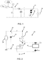
- Figure 1 shows in schematic form three possible general approaches for providing a modulated output current to an LED load 10.
- a first approach is to achieve current modulation based on modified control of the main driver, which is typically a switch mode power converter.
- An analogue input voltage "Vref” or else a digital pulse width modulation disable signal “PWM disable” controls a transmission gate 12 at the output of the driver. This works well for slow data, for example data at less than 20 kbits/second, corresponding to the switching frequency of the switch mode power converter.
- a second approach is to use a parallel shunt 14. This turns off the LED by providing a bypass for the LED current. This can waste a substantial amount of energy.
- a third approach is to use a linear modulator 16. This provides a current modification by controlling a transistor which functions as a current regulator in series with the LED load 10. This is a more power-efficient solution.
- the output of the driver has an output capacitor.
- the output capacitor should be very small, whereas for the third approach, it should be very large.
- the linear modulator functions as a current control element for controlling the current between fixed voltage rails.
- the linear modulator comprises a MOS transistor with a controlled source-drain current.
- the resulting current flowing may be used as a feedback control parameter to control the modulation function.
- a current-regulating LED driver in series with a currentmodulating transistor is known to be difficult to control.
- the circuit comprises two current sources in series: the LED driver which is the source and the current modulator that acts as the load. With a minor mismatch between these two currents, clipping of the modulation current may occur or a rapid escalation of output voltage of the driver may occur that also causes dramatic power losses in the current modulator.
- EP 2 547 174 shows the use of a linear modulator according to the third approach wherein a current feedback loop is provided to the driver for maintaining a constant average current in the LEDs.
- the feedback loop of EP 2 547 174 comprises a low pass filter in such a way that the modulated current is minimized in the feedback loop.
- Such feedback loop does not compensate a possible drift in the output voltage of the driver because it only takes into account the average current.
- a current modulator circuit for modulating a drive current through a lighting load, comprising:
- This modulator circuit provides two feedback control paths. One operates at a relatively low frequency, for example at DC, and the control is based on a voltage across the current modulating element. The average DC voltage obtained by low pass filtering is representative of the average voltage at the output of the driver. This voltage feedback thus stabilizes the general steady state operating conditions of the current modulating element.
- the second feedback path operates provides the data modulation. In this way, a compensation can be made on the modulating current to match a constant input current provided by the driver for preventing voltage drift.
- the current modulating element for example comprises a transistor (such as a MOSFET, other type of FET or other type of transistor) or any other controllable semiconductor device.
- the feedback based on the voltage across the current modulating element aims to keep the current modulating element in a well-defined operational mode, while at the same time keeping the losses low.
- An error between the supply current to the current modulating circuit and the average current through the current modulating element can be measured over an integrated time as a voltage difference between an operating voltage of the current modulating circuit and the lighting load voltage.
- a voltage drop provides headroom for the current modulating element to regulate the average current and the modulation current. Too little voltage headroom will deteriorate the modulation current and too high headroom voltage will result in excessive power losses.
- a capacitance decrease increases the voltage peak-to-peak amplitude), which both have an influence on the operation of the current modulating element a lowest voltage can be monitored and used as a feedback signal. In this way, the voltage across the current modulating element takes a dynamic value which depends on the nature of the lighting load.
- the invention is thus based on controlling a low frequency (e.g. DC average) voltage of the current modulating element or controlling a peak (e.g. minimal) voltage to be equal to a reference control voltage.
- a low frequency (e.g. DC average) voltage of the current modulating element or controlling a peak (e.g. minimal) voltage to be equal to a reference control voltage.
- An AC (high frequency) current through the LED load is controlled in proportion to the modulating data signal.
- the first feedback control path (e.g. DC control loop) for example comprises an operational amplifier, for example including an integrator function and proportional-integral control, to measure and regulate the voltage across the current modulating element towards a reference voltage.
- the measured voltage is for example the average voltage across the current modulating element or it may be a peak voltage across the current modulating element, in particular the minimum peak voltage across the current modulating element.
- the requirements for the average voltage drop across the current modulating element strongly depends on the V-I characteristics of the lighting load (which varies for different lighting load types) and the configuration of the lighting load such as the number of lighting elements in series and parallel, as well as average current and modulation depth.
- the minimum peak voltage provides a measure of the headroom provided by the current modulating element. By ensuring this is at a low level, the efficiency of the system is improved by maintaining low losses.
- the ESR (equivalent series resistance) of LEDs is dependent on the drive current: typically the ESR increases at lower current levels e.g. when dimming the luminaire. Optimization of the modulation efficiency requires a minimum average voltage drop across the modulator and a minimum voltage across the modulator is required to ensure that the modulation signal does not get distorted.
- the drive current needs the ability to adapt its average voltage drop in order to improve efficiency. For this reason, a good input signal to control the average voltage drop across the modulator in a dynamic way is indeed the minimum voltage across the modulator (so that it never gets saturated).
- the current modulating element for example comprises a transistor as explained above and the reference voltage is then selected such that the transistor operates in the linear mode but close to the limit of saturation. This provides efficient operation of the circuit.
- the feedback system may comprise a filter between an output of the current modulating element and a control input of the current modulating element. This is used to enable control based on the DC current flowing.
- the filter for example comprises a low pass filter. It may be implemented as a proportional-integral filter.
- the data input signal may be provided to one terminal of the filter.
- This provides a joint high frequency (AC) and low frequency (DC) control loop.
- the first (DC) feedback control path is based on a voltage associated with the current modulating element, and the second (AC) feedback control path is implemented by injecting the data input signal. This provides a closed loop AC control.
- an AC control loop may be based on measurement of the current through the current modulating transistor, wherein the current through the current modulating transistor is compared with the data input signal, and the result is provided to one terminal of the low pass filter through a high pass filter.
- the high pass filter operates at a higher frequency than the low pass filter.
- This provides separate closed loop AC and DC control loops for the low frequency and high frequency feedback control paths.
- the AC control loop may furthermore include an input signal based on measurement of the optical output of the LED load. This enables different optical efficiencies to be taken into account.
- the modulator can also be designed such that it suppresses a mains ripple that usually appears at the output of a single stage LED driver. To do so, the LED current can be measured and fed through a filter and then be applied to the modulator input signal.
- the invention also provides a driving circuit for driving a lighting load, comprising:
- This circuit makes use of a capacitor to enable the output current from the driver and the current through the lighting load to differ over short time scales, but the average current over time is the same.
- the current modulating element thus delivers an average current which is equal to the delivered current by the driver.
- the variation is a superimposed modulated current on top of the average current.
- the feedback system ensures the average currents remain equal.
- the first feedback control path sets the operating point for the current modulating element, and provides a match between the overall driver current and the lighting load integrated current over time.
- the second feedback control path implements the data modulation, and the fluctuations between the driver current and the lighting load current result in charge flow to and from the capacitor.
- the invention also provides a lighting circuit comprising:
- the lighting load preferably comprises an LED arrangement comprising series and/or parallel LEDs.
- the invention provides a current modulating circuit, for example for use in a driving circuit for driving a lighting load such as an LED arrangement.
- a current modulating element is provided in series with the lighting load, and modulates the current based on a data input signal.
- a feedback system controls the current modulating element, and it has a first feedback control path which uses a voltage across the current modulating element, and a second feedback control path which uses the data input signal. The difference in current is taken up by a capacitor at the output of the driver. The voltage feedback is used to avoid a drift of the voltage across the capacitor at the output of the driver while the average current is maintained close to the current outputted by the driver.
- FIG 2 shows an example of a driving circuit 20 for driving a lighting load such as an LED load 22.
- the driving circuit 20 is all parts shown in Figure 2 apart from the LED load 22.
- An LED driver is shown as a current source 24, which represents a (typically switch mode) power supply which delivers a controlled current between first and second driver output terminals 26, 28. These output terminals connect to a current modulator circuit for controlling the current supplied to the LED load.
- An output capacitor 30 is connected between the first and second driver output terminals 26, 28 and it absorbs or delivers current so that the driver output current may be constant even while the load current varies.
- the circuit 20 has first and second driving circuit outputs 32, 34, for connection to the LED load 22.
- the first driving circuit output 32 is connected to the first driver output terminal 26, and the second driving circuit output 34 is connected to the second driver output terminal 28 through the current modulating transistor 36.
- the transistor 36 may instead be at the high side (so that the terminal 28 may instead be considered to be the "first" driver output terminal).
- a feedback system 38 is provided for controlling the current modulating transistor 36 thereby to implement modulation of the current through the LED load 22.
- the feedback system 38 comprises a first input Vmod of a voltage across the current modulating transistor 36, and a second input of the data input signal Vdata. These two inputs implement separate feedback control paths, which operate at different frequencies. One control path is a low frequency steady state control path and the other is a high frequency data modulation control path.
- the operating range of the transistor 36 is for example guaranteed by controlling the average voltage across the source-drain of the transistor.
- a current difference between the supply current of the LED driver 24 and the average current through the transistor 36 is monitored over time based on the voltage difference between the LED driver output 26, 28 and the LED voltage.
- the voltage drop across the transistor 36 provides headroom for the transistor to regulate both the average current and also the modulation current. Too little voltage headroom will deteriorate the modulation current and too high headroom voltage will result in excessive power losses.
- the voltage resulting from the highest current may be monitored. This corresponds to the lowest voltage. This enables the system to tolerate current intensity dimming, wherein the current dimming shifts down the average voltage. Similarly, the aging of the electrolytic capacitor 30 may be compensated. These both have an influence on the transistor operation.
- the feedback system 38 includes a filter 40, in particular a low pass filter so that only the slow average voltage variations (in the voltage Vmod across the transistor) are used as feedback parameter.
- the low pass filter may comprise a proportional-integral (PI) filter.
- the filter is between an output (e.g. drain) of the current modulating transistor 36 and a control input (e.g. gate) of the current modulating transistor 36.
- the circuit of Figure 2 has a single loop which combines the two feedback control paths.
- the filter 40 implements a DC feedback control path, and the data input signal Vdata is provided to one terminal of the filter and thereby adds an AC control path to the single loop.
- a first difference voltage between the measured voltage Vmod and a reference voltage Vref is generated using an adder (with negative input for Vmod, i.e. a subtractor/comparator implemented using an operational amplifier) and the data voltage Vdata is added into the control loop.
- Vdata AC feedback control path
- Vref DC feedback control path
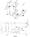
- Figure 3 shows an alternative design with two control loops for the two feedback control paths.
- the DC control loop comprises the low pass filter 40 as explained above.
- the AC control loop is based on measurement of the current through the current modulating transistor 36 using a current sensing resistor 42 in series with the transistor 36 and LED load 22.
- a signal based on the current through the current modulating transistor 36 (in particular the voltage across the current sensing resistor) is compared with the data input signal Vdata, and the result is provided to one terminal of the low pass filter through a high pass filter 44.
- a first difference voltage between the measured voltage Vmod and a reference voltage Vref is generated using an adder (with negative input for Vmod, i.e. a subtractor/comparators implemented using an operational amplifier).
- a second difference voltage between the sensed voltage across the resistor 42 and the data voltage is generated using a second adder (with negative input for the resistor voltage, i.e. a subtractor/comparator implemented using an operational amplifier). The high pass filtered result is then added into the DC control loop.
- the AC control path may be implemented by directly coupling the modulating signal to the control input of the transistor thereby providing open loop feedforward control ( Figure 2 ), or by using a feedback loop that compares the actual transistor or LED load current with the modulating signal and feeding the difference via a feedback loop with a high pass filter ( Figure 3 ).
- the high pass filter blocks DC.
- a combination of an open loop control for high speed data and a closed loop for lower frequency data may also be used to reduce flicker coming from the main power driver.
- the measured LED current can be fed through a filter and then be applied to the modulator input signal.
- the DC control loop keeps the transistor in a well-defined operational mode at the same time as keeping the losses low, for example operating in the linear mode, but close to the saturation point for low losses.
- the transistor By operating in the linear mode, the transistor functions as a controllable current source. For example, if the voltage across the transistor increases, a larger portion of the driver current flows into the capacitor and thus less current flows through the LEDs.
- the voltage reference Vref may be a constant voltage level. However, it may also be adaptive to ensure that it is just large enough to enable the desired modulation depth of the light output of the LED load. For example, the modulator can automatically adapt to an unknown number of LEDs, or to a variable current from the driver and enable a variable modulation depth to be implemented. This approach is explained in detail below with reference to Figure 6 .
- the voltage margin that the transistor should handle is linearly dependent on the number of LEDs in series with the transistor.
- the voltage margin is also linearly dependent on the current intensity, which is relevant for example for a dimmable driver.
- the voltage margin is also linearly dependent on the modulation depth.
- the AC feedback loop may also use measurement of the LED optical output.
- nonlinearity in the LED output can also be taken into account.
- the voltage across the transistor can be slowly reduced to almost zero. This limits the losses of the modulator when no modulation is applied.
- Automatic adjustment of the reference voltage and voltage reduction across the transistor during long periods of no modulation may instead be achieved by the DC feedback loop, when the minimal peak voltage on the drain (or collector) of the transistor is used as the feedback parameter.
- the reference voltage Vref may be dynamically adjustable so that it can be set according to different drive current, LEDs, and LED configuration. For fixed output and fixed LEDs luminaires, Vref can be set at a fixed value.
- the voltage drop across the transistor should be as low as possible.
- the necessary voltage swing depends on number of LEDs, current intensity and modulation depth.
- a circuit that measures the minimal voltage on the source (or emitter) enables this control, by providing a feedback loop that regulates this minimal peak voltage to a reference Vref. In this way, the optimal efficiency is ensured for all variations in number of LEDs, current intensity and modulation depth, avoiding saturation of the transistor.
- the transistor is controlled in an analog manner, functioning as an analog controllable current source.
- the transistor may instead be operated in a hard on-off mode at a fast switching rate.
- the transistor may in this way perform pulse width modulation.
- the AC and DC control loops may then be operated at frequencies sufficiently below the switching rate.
- the AC control loop will also filter the PWM signal.
- the AC control loop should have a pass through band from a few hundreds of Hz to a few kHz (and below 16 kHz) .
- the AC control loop may also control the LED current at double the mains frequency i.e. 100 Hz or 120 Hz. In that case, ripple from the main driver is reduced.
- the circuit may then be used as a ripple reduction circuit.
- Figure 4 shows a simulated circuit.
- the LED driver 24 is simulated as an ideal current source I1, an overvoltage protection realized by diode D2 and voltage source V1, an output diode D3 and the output capacitor C1.
- the coded light injector comprises the input capacitor 30 (C2) the transistor 36 (Q1) and the current sense resistor 42 (R42).
- VCTRL The low pass filtered version of the voltage Vmod is provided as VCTRL and the high pass filtered version of the comparison result of the sensed current (I_DC) and the data input is provided as VCTRL2 They are summed at the gate of the transistor 36.
- Figure 5 shows simulation results.
- the top plot shows the LED power.
- the second plot shows the power losses within the modulating transistor Q1.
- the third plot shows the data input and the bottom plot shows the LED current.
- Figure 6 shows a second example of a circuit which makes use of detection of the minimum voltage across the current modulating element.
- Figure 6A shows:
- the circuit of Figure 6A connects to the circuit of Figure 6B at the nodes shown as X and Y.
- Figure 6B shows a minimum peak detector 72.
- the transistor M1 in Figure 6A is the modulation transistor.
- the LED current is sensed via resistor R16 of the current sense circuit 68 and it is averaged via the low pass filter R14 and C2 within the average current setting circuit 66.
- the voltage across C2 represents the average LED current and is fed to the '+' input of the operational amplifier U1 within the current regulation unit 62.
- the instantaneous LED current is sensed via R10 and R16 (R10 can be 0 ohm) within the LED current sense circuit.
- This signal is fed to the '-' input of the operational amplifier U1 in the current regulation unit 62.
- the error signal difference voltage between the '+' and '-'
- the operational amplifier U1 and its feedback capacitor C10 forms a PI controller.
- the error signal is integrated and the output of the operational amplifier U1 provides a driving signal for the modulation transistor M1.
- the drain voltage of the transistor M1 is sensed via the divider R7 and R8 in the average drain voltage detector circuit 70. This voltage is then averaged by C2 and R5 in the average current setting circuit 66. Therefore, only the average drain voltage is added to the feedback circuit. This is a slow reacting loop.
- the data modulation is injected to the '-' input of the operational amplifier U1 via AC coupling of capacitor C9 within the amplitude modulation circuit 60. This adds the data modulation to the instantaneous current sense value. This is a closed loop modulation.
- the resistor R27 determines the modulation depth.
- the feedback loop will suppress the low frequency modulation (e.g. 100Hz ripple from the LED driver) due to low-pass filter in loop 66, while letting the high frequency modulation (the data) pass through a proper tuning of the bandwidth of the feedback loop 64. In this way the low frequency ripple is removed by the modulator and the LED current will not contain the low frequency ripple, rather only the high frequency modulation data.
- the low frequency modulation e.g. 100Hz ripple from the LED driver
- the high frequency modulation the data
- the circuit also comprises a minimum peak detector shown in Figure 6B .
- This circuit senses the valley of the drain voltage via a fast-reacting circuit.
- the drain voltage charges the capacitor C7 via D5 and R9.
- This circuit has long time constant.
- the Vcc voltage also charges C7 and tries to keep C7 at high level.
- the discharging of C7 is directly via D2 and thus has a much faster time constant. In this way, the voltage across C7 will represent the valley voltage of the drain of the transistor M1 (i.e. the minimum peak).
- This signal is further filtered by R13, R6, C8 and D10.
- the voltage at capacitor C8 is a clean signal, representing the minimum peak voltage of the drain.
- the operational amplifier U2 compares the minimum peak to a (constant) setpoint provided by the divider R15 and R19. The output of U2 is injected to the '+' input node of U1. In this way, the feedback loop will maintain the minimum peak of the drain voltage to a constant level. In this way, the average drain voltage is controlled in a dynamic way and depends on the LED current, LED type, modulation depth and electrolytic capacitance and age, etc.
- This circuit shows how the voltage across the current modulating transistor is effectively controlled in a dynamic way, by instead using detection of a minimum valley current and setting this to a constant level.
- the invention is of relevance generally to lighting applications in which data is modulated through light such as so-called coded light and so-called LiFi.
- Indoor positioning systems may for example make use of coded visual light communication.
- the invention instead enables energy efficient current ripple reduction of a low-cost driver or ballast.
Landscapes
- Engineering & Computer Science (AREA)
- Power Engineering (AREA)
- Physics & Mathematics (AREA)
- Electromagnetism (AREA)
- Computer Networks & Wireless Communication (AREA)
- Signal Processing (AREA)
- Circuit Arrangement For Electric Light Sources In General (AREA)
- Optical Communication System (AREA)
Applications Claiming Priority (2)
| Application Number | Priority Date | Filing Date | Title |
|---|---|---|---|
| EP16195066 | 2016-10-21 | ||
| PCT/EP2017/075929 WO2018073069A1 (en) | 2016-10-21 | 2017-10-11 | A current modulation circuit, a driving circuit, and a method for driving a lighting load with current modulation |
Publications (2)
| Publication Number | Publication Date |
|---|---|
| EP3529922A1 EP3529922A1 (en) | 2019-08-28 |
| EP3529922B1 true EP3529922B1 (en) | 2021-04-14 |
Family
ID=57206042
Family Applications (1)
| Application Number | Title | Priority Date | Filing Date |
|---|---|---|---|
| EP17780138.8A Active EP3529922B1 (en) | 2016-10-21 | 2017-10-11 | A current modulation circuit, a driving circuit, and a method for driving a lighting load with current modulation |
Country Status (5)
| Country | Link |
|---|---|
| US (1) | US10602575B2 (https=) |
| EP (1) | EP3529922B1 (https=) |
| JP (1) | JP7101667B2 (https=) |
| CN (1) | CN109863702B (https=) |
| WO (1) | WO2018073069A1 (https=) |
Families Citing this family (3)
| Publication number | Priority date | Publication date | Assignee | Title |
|---|---|---|---|---|
| CN113423162B (zh) * | 2021-04-27 | 2023-04-25 | 安波福电子(苏州)有限公司 | 一种用于对照明系统的控制电流进行校准的方法 |
| FR3124042B1 (fr) * | 2021-06-09 | 2026-01-02 | Commissariat Energie Atomique | Convertisseur de puissance |
| CN118101046B (zh) * | 2024-04-29 | 2024-07-23 | 南昌大学 | 一种led阵列的等效电路结构和照明通信联合性能分析系统 |
Family Cites Families (16)
| Publication number | Priority date | Publication date | Assignee | Title |
|---|---|---|---|---|
| JPH0758704A (ja) * | 1993-08-13 | 1995-03-03 | Ricoh Co Ltd | 光通信制御装置 |
| JP5195193B2 (ja) * | 2008-09-11 | 2013-05-08 | 東芝ライテック株式会社 | 電源装置及び照明器具 |
| JP5906408B2 (ja) * | 2011-07-15 | 2016-04-20 | パナソニックIpマネジメント株式会社 | 照明光通信装置及びそれを用いた照明器具、並びに照明システム |
| JP6010284B2 (ja) * | 2011-08-11 | 2016-10-19 | ローム株式会社 | スイッチングレギュレータおよびその制御回路、制御方法、ならびに電子機器 |
| KR101877371B1 (ko) * | 2011-10-14 | 2018-07-12 | 삼성전자주식회사 | 전원 변조기를 보호하기 위한 장치 및 방법 |
| CN102695343B (zh) * | 2012-06-06 | 2014-01-29 | 矽力杰半导体技术(杭州)有限公司 | 一种led驱动电路 |
| US8803445B2 (en) * | 2012-09-07 | 2014-08-12 | Infineon Technologies Austria Ag | Circuit and method for driving LEDs |
| US9374855B2 (en) * | 2013-10-24 | 2016-06-21 | Osram Sylvania Inc. | Power line communication for lighting systems |
| CN104768263B (zh) * | 2014-01-02 | 2018-11-27 | 深圳市海洋王照明工程有限公司 | 自适应led升压驱动电路 |
| FR3019268A1 (fr) | 2014-03-26 | 2015-10-02 | Luciom | Dispositif de commande de l'intensite lumineuse d'ambiance d'un systeme d'eclairage et de transfert de donnees |
| US9351352B2 (en) * | 2014-04-03 | 2016-05-24 | Linear Technology Corporation | Boost then floating buck mode converter for LED driver using common switch control signal |
| EP3113578B1 (en) * | 2015-06-30 | 2018-08-08 | Nxp B.V. | A filter circuit |
| JP6699073B2 (ja) * | 2016-03-25 | 2020-05-27 | ヤマハ株式会社 | 自励式d級増幅器 |
| JP6799819B2 (ja) * | 2017-01-30 | 2020-12-16 | パナソニックIpマネジメント株式会社 | 点灯装置、照明器具及び看板 |
| CN107094329B (zh) * | 2017-05-03 | 2019-01-29 | 矽力杰半导体技术(杭州)有限公司 | Led驱动电路 |
| US10310528B1 (en) * | 2017-12-06 | 2019-06-04 | Silicon Laboratories Inc. | System and method for correcting offset voltage errors within a band gap circuit |
-
2017
- 2017-10-11 JP JP2019520027A patent/JP7101667B2/ja active Active
- 2017-10-11 CN CN201780064831.7A patent/CN109863702B/zh active Active
- 2017-10-11 US US16/341,913 patent/US10602575B2/en active Active
- 2017-10-11 WO PCT/EP2017/075929 patent/WO2018073069A1/en not_active Ceased
- 2017-10-11 EP EP17780138.8A patent/EP3529922B1/en active Active
Non-Patent Citations (1)
| Title |
|---|
| None * |
Also Published As
| Publication number | Publication date |
|---|---|
| WO2018073069A1 (en) | 2018-04-26 |
| CN109863702A (zh) | 2019-06-07 |
| CN109863702B (zh) | 2022-09-23 |
| US10602575B2 (en) | 2020-03-24 |
| EP3529922A1 (en) | 2019-08-28 |
| JP2019537868A (ja) | 2019-12-26 |
| JP7101667B2 (ja) | 2022-07-15 |
| US20190246465A1 (en) | 2019-08-08 |
Similar Documents
| Publication | Publication Date | Title |
|---|---|---|
| US8680787B2 (en) | Load control device for a light-emitting diode light source | |
| KR100960825B1 (ko) | Led 어레이를 구동하기 위한 스위칭 디바이스 | |
| US8803445B2 (en) | Circuit and method for driving LEDs | |
| US10412796B2 (en) | LED drive circuit with a programmable input for LED lighting | |
| US8680781B1 (en) | Circuit and method for driving LEDs | |
| US8319445B2 (en) | Modified dimming LED driver | |
| US10278242B2 (en) | Thermal and power optimization for linear regulator | |
| US7688053B2 (en) | Variable voltage regulating device | |
| US10136487B2 (en) | Power optimization for linear regulator | |
| EP3113578B1 (en) | A filter circuit | |
| US20140184076A1 (en) | Low intensity dimming circuit for an led lamp and method of controlling an led | |
| KR20080087819A (ko) | 전자 디바이스에 공급되는 전류를 제어하는 방법 및 장치 | |
| EP2716134A1 (en) | A method of driving led lighting sources and related device | |
| US10492259B2 (en) | Dimmable LED driver and dimming method | |
| EP3529922B1 (en) | A current modulation circuit, a driving circuit, and a method for driving a lighting load with current modulation | |
| US10306718B1 (en) | Light emitting device driver apparatus with multiple dimming modes and conversion control circuit thereof | |
| JP2017534155A (ja) | ドライバ回路及び方法 | |
| WO2016049671A1 (en) | Switched direct ac driver for leds | |
| EP3139483A1 (en) | Electronic reverse buck converter, and corresponding method of operating an electronic reverse buck converter | |
| GB2517455A (en) | Light Apparatus | |
| WO2016131719A1 (en) | Level control circuit and method | |
| Pai et al. | Design and prototyping of dimmable LED driver for general lighting application | |
| CN210579380U (zh) | 照明驱动电路以及照明系统 | |
| KR20150046980A (ko) | Triac 제어를 이용한 엘이디 조명 장치 | |
| KR20150046495A (ko) | Dc/dc 컨버터 |
Legal Events
| Date | Code | Title | Description |
|---|---|---|---|
| STAA | Information on the status of an ep patent application or granted ep patent |
Free format text: STATUS: UNKNOWN |
|
| STAA | Information on the status of an ep patent application or granted ep patent |
Free format text: STATUS: THE INTERNATIONAL PUBLICATION HAS BEEN MADE |
|
| PUAI | Public reference made under article 153(3) epc to a published international application that has entered the european phase |
Free format text: ORIGINAL CODE: 0009012 |
|
| STAA | Information on the status of an ep patent application or granted ep patent |
Free format text: STATUS: REQUEST FOR EXAMINATION WAS MADE |
|
| 17P | Request for examination filed |
Effective date: 20190521 |
|
| AK | Designated contracting states |
Kind code of ref document: A1 Designated state(s): AL AT BE BG CH CY CZ DE DK EE ES FI FR GB GR HR HU IE IS IT LI LT LU LV MC MK MT NL NO PL PT RO RS SE SI SK SM TR |
|
| AX | Request for extension of the european patent |
Extension state: BA ME |
|
| DAV | Request for validation of the european patent (deleted) | ||
| DAX | Request for extension of the european patent (deleted) | ||
| STAA | Information on the status of an ep patent application or granted ep patent |
Free format text: STATUS: EXAMINATION IS IN PROGRESS |
|
| 17Q | First examination report despatched |
Effective date: 20200602 |
|
| REG | Reference to a national code |
Ref country code: DE Ref legal event code: R079 Ref document number: 602017036743 Country of ref document: DE Free format text: PREVIOUS MAIN CLASS: H04B0010116000 Ipc: H05B0045395000 |
|
| RIC1 | Information provided on ipc code assigned before grant |
Ipc: H05B 47/165 20200101ALI20201006BHEP Ipc: H05B 45/395 20200101AFI20201006BHEP Ipc: H04B 10/116 20130101ALI20201006BHEP |
|
| GRAP | Despatch of communication of intention to grant a patent |
Free format text: ORIGINAL CODE: EPIDOSNIGR1 |
|
| STAA | Information on the status of an ep patent application or granted ep patent |
Free format text: STATUS: GRANT OF PATENT IS INTENDED |
|
| INTG | Intention to grant announced |
Effective date: 20201113 |
|
| GRAS | Grant fee paid |
Free format text: ORIGINAL CODE: EPIDOSNIGR3 |
|
| GRAA | (expected) grant |
Free format text: ORIGINAL CODE: 0009210 |
|
| STAA | Information on the status of an ep patent application or granted ep patent |
Free format text: STATUS: THE PATENT HAS BEEN GRANTED |
|
| AK | Designated contracting states |
Kind code of ref document: B1 Designated state(s): AL AT BE BG CH CY CZ DE DK EE ES FI FR GB GR HR HU IE IS IT LI LT LU LV MC MK MT NL NO PL PT RO RS SE SI SK SM TR |
|
| REG | Reference to a national code |
Ref country code: GB Ref legal event code: FG4D |
|
| REG | Reference to a national code |
Ref country code: CH Ref legal event code: EP |
|
| REG | Reference to a national code |
Ref country code: DE Ref legal event code: R096 Ref document number: 602017036743 Country of ref document: DE |
|
| REG | Reference to a national code |
Ref country code: IE Ref legal event code: FG4D |
|
| REG | Reference to a national code |
Ref country code: AT Ref legal event code: REF Ref document number: 1383627 Country of ref document: AT Kind code of ref document: T Effective date: 20210515 |
|
| REG | Reference to a national code |
Ref country code: LT Ref legal event code: MG9D |
|
| REG | Reference to a national code |
Ref country code: AT Ref legal event code: MK05 Ref document number: 1383627 Country of ref document: AT Kind code of ref document: T Effective date: 20210414 |
|
| REG | Reference to a national code |
Ref country code: NL Ref legal event code: MP Effective date: 20210414 |
|
| PG25 | Lapsed in a contracting state [announced via postgrant information from national office to epo] |
Ref country code: FI Free format text: LAPSE BECAUSE OF FAILURE TO SUBMIT A TRANSLATION OF THE DESCRIPTION OR TO PAY THE FEE WITHIN THE PRESCRIBED TIME-LIMIT Effective date: 20210414 Ref country code: LT Free format text: LAPSE BECAUSE OF FAILURE TO SUBMIT A TRANSLATION OF THE DESCRIPTION OR TO PAY THE FEE WITHIN THE PRESCRIBED TIME-LIMIT Effective date: 20210414 Ref country code: NL Free format text: LAPSE BECAUSE OF FAILURE TO SUBMIT A TRANSLATION OF THE DESCRIPTION OR TO PAY THE FEE WITHIN THE PRESCRIBED TIME-LIMIT Effective date: 20210414 Ref country code: BG Free format text: LAPSE BECAUSE OF FAILURE TO SUBMIT A TRANSLATION OF THE DESCRIPTION OR TO PAY THE FEE WITHIN THE PRESCRIBED TIME-LIMIT Effective date: 20210714 Ref country code: AT Free format text: LAPSE BECAUSE OF FAILURE TO SUBMIT A TRANSLATION OF THE DESCRIPTION OR TO PAY THE FEE WITHIN THE PRESCRIBED TIME-LIMIT Effective date: 20210414 Ref country code: HR Free format text: LAPSE BECAUSE OF FAILURE TO SUBMIT A TRANSLATION OF THE DESCRIPTION OR TO PAY THE FEE WITHIN THE PRESCRIBED TIME-LIMIT Effective date: 20210414 |
|
| PG25 | Lapsed in a contracting state [announced via postgrant information from national office to epo] |
Ref country code: GR Free format text: LAPSE BECAUSE OF FAILURE TO SUBMIT A TRANSLATION OF THE DESCRIPTION OR TO PAY THE FEE WITHIN THE PRESCRIBED TIME-LIMIT Effective date: 20210715 Ref country code: IS Free format text: LAPSE BECAUSE OF FAILURE TO SUBMIT A TRANSLATION OF THE DESCRIPTION OR TO PAY THE FEE WITHIN THE PRESCRIBED TIME-LIMIT Effective date: 20210814 Ref country code: SE Free format text: LAPSE BECAUSE OF FAILURE TO SUBMIT A TRANSLATION OF THE DESCRIPTION OR TO PAY THE FEE WITHIN THE PRESCRIBED TIME-LIMIT Effective date: 20210414 Ref country code: RS Free format text: LAPSE BECAUSE OF FAILURE TO SUBMIT A TRANSLATION OF THE DESCRIPTION OR TO PAY THE FEE WITHIN THE PRESCRIBED TIME-LIMIT Effective date: 20210414 Ref country code: PT Free format text: LAPSE BECAUSE OF FAILURE TO SUBMIT A TRANSLATION OF THE DESCRIPTION OR TO PAY THE FEE WITHIN THE PRESCRIBED TIME-LIMIT Effective date: 20210816 Ref country code: PL Free format text: LAPSE BECAUSE OF FAILURE TO SUBMIT A TRANSLATION OF THE DESCRIPTION OR TO PAY THE FEE WITHIN THE PRESCRIBED TIME-LIMIT Effective date: 20210414 Ref country code: LV Free format text: LAPSE BECAUSE OF FAILURE TO SUBMIT A TRANSLATION OF THE DESCRIPTION OR TO PAY THE FEE WITHIN THE PRESCRIBED TIME-LIMIT Effective date: 20210414 Ref country code: NO Free format text: LAPSE BECAUSE OF FAILURE TO SUBMIT A TRANSLATION OF THE DESCRIPTION OR TO PAY THE FEE WITHIN THE PRESCRIBED TIME-LIMIT Effective date: 20210714 |
|
| REG | Reference to a national code |
Ref country code: DE Ref legal event code: R097 Ref document number: 602017036743 Country of ref document: DE |
|
| PG25 | Lapsed in a contracting state [announced via postgrant information from national office to epo] |
Ref country code: SM Free format text: LAPSE BECAUSE OF FAILURE TO SUBMIT A TRANSLATION OF THE DESCRIPTION OR TO PAY THE FEE WITHIN THE PRESCRIBED TIME-LIMIT Effective date: 20210414 Ref country code: SK Free format text: LAPSE BECAUSE OF FAILURE TO SUBMIT A TRANSLATION OF THE DESCRIPTION OR TO PAY THE FEE WITHIN THE PRESCRIBED TIME-LIMIT Effective date: 20210414 Ref country code: CZ Free format text: LAPSE BECAUSE OF FAILURE TO SUBMIT A TRANSLATION OF THE DESCRIPTION OR TO PAY THE FEE WITHIN THE PRESCRIBED TIME-LIMIT Effective date: 20210414 Ref country code: DK Free format text: LAPSE BECAUSE OF FAILURE TO SUBMIT A TRANSLATION OF THE DESCRIPTION OR TO PAY THE FEE WITHIN THE PRESCRIBED TIME-LIMIT Effective date: 20210414 Ref country code: EE Free format text: LAPSE BECAUSE OF FAILURE TO SUBMIT A TRANSLATION OF THE DESCRIPTION OR TO PAY THE FEE WITHIN THE PRESCRIBED TIME-LIMIT Effective date: 20210414 Ref country code: RO Free format text: LAPSE BECAUSE OF FAILURE TO SUBMIT A TRANSLATION OF THE DESCRIPTION OR TO PAY THE FEE WITHIN THE PRESCRIBED TIME-LIMIT Effective date: 20210414 Ref country code: ES Free format text: LAPSE BECAUSE OF FAILURE TO SUBMIT A TRANSLATION OF THE DESCRIPTION OR TO PAY THE FEE WITHIN THE PRESCRIBED TIME-LIMIT Effective date: 20210414 |
|
| PLBE | No opposition filed within time limit |
Free format text: ORIGINAL CODE: 0009261 |
|
| STAA | Information on the status of an ep patent application or granted ep patent |
Free format text: STATUS: NO OPPOSITION FILED WITHIN TIME LIMIT |
|
| 26N | No opposition filed |
Effective date: 20220117 |
|
| REG | Reference to a national code |
Ref country code: CH Ref legal event code: PL |
|
| PG25 | Lapsed in a contracting state [announced via postgrant information from national office to epo] |
Ref country code: IS Free format text: LAPSE BECAUSE OF FAILURE TO SUBMIT A TRANSLATION OF THE DESCRIPTION OR TO PAY THE FEE WITHIN THE PRESCRIBED TIME-LIMIT Effective date: 20210814 Ref country code: AL Free format text: LAPSE BECAUSE OF FAILURE TO SUBMIT A TRANSLATION OF THE DESCRIPTION OR TO PAY THE FEE WITHIN THE PRESCRIBED TIME-LIMIT Effective date: 20210414 |
|
| REG | Reference to a national code |
Ref country code: BE Ref legal event code: MM Effective date: 20211031 |
|
| PG25 | Lapsed in a contracting state [announced via postgrant information from national office to epo] |
Ref country code: MC Free format text: LAPSE BECAUSE OF FAILURE TO SUBMIT A TRANSLATION OF THE DESCRIPTION OR TO PAY THE FEE WITHIN THE PRESCRIBED TIME-LIMIT Effective date: 20210414 |
|
| PG25 | Lapsed in a contracting state [announced via postgrant information from national office to epo] |
Ref country code: LU Free format text: LAPSE BECAUSE OF NON-PAYMENT OF DUE FEES Effective date: 20211011 Ref country code: IT Free format text: LAPSE BECAUSE OF FAILURE TO SUBMIT A TRANSLATION OF THE DESCRIPTION OR TO PAY THE FEE WITHIN THE PRESCRIBED TIME-LIMIT Effective date: 20210414 Ref country code: BE Free format text: LAPSE BECAUSE OF NON-PAYMENT OF DUE FEES Effective date: 20211031 |
|
| PG25 | Lapsed in a contracting state [announced via postgrant information from national office to epo] |
Ref country code: LI Free format text: LAPSE BECAUSE OF NON-PAYMENT OF DUE FEES Effective date: 20211031 Ref country code: CH Free format text: LAPSE BECAUSE OF NON-PAYMENT OF DUE FEES Effective date: 20211031 |
|
| PG25 | Lapsed in a contracting state [announced via postgrant information from national office to epo] |
Ref country code: IE Free format text: LAPSE BECAUSE OF NON-PAYMENT OF DUE FEES Effective date: 20211011 |
|
| P01 | Opt-out of the competence of the unified patent court (upc) registered |
Effective date: 20230425 |
|
| PG25 | Lapsed in a contracting state [announced via postgrant information from national office to epo] |
Ref country code: CY Free format text: LAPSE BECAUSE OF FAILURE TO SUBMIT A TRANSLATION OF THE DESCRIPTION OR TO PAY THE FEE WITHIN THE PRESCRIBED TIME-LIMIT Effective date: 20210414 |
|
| PG25 | Lapsed in a contracting state [announced via postgrant information from national office to epo] |
Ref country code: HU Free format text: LAPSE BECAUSE OF FAILURE TO SUBMIT A TRANSLATION OF THE DESCRIPTION OR TO PAY THE FEE WITHIN THE PRESCRIBED TIME-LIMIT; INVALID AB INITIO Effective date: 20171011 |
|
| PG25 | Lapsed in a contracting state [announced via postgrant information from national office to epo] |
Ref country code: MK Free format text: LAPSE BECAUSE OF FAILURE TO SUBMIT A TRANSLATION OF THE DESCRIPTION OR TO PAY THE FEE WITHIN THE PRESCRIBED TIME-LIMIT Effective date: 20210414 |
|
| PG25 | Lapsed in a contracting state [announced via postgrant information from national office to epo] |
Ref country code: TR Free format text: LAPSE BECAUSE OF FAILURE TO SUBMIT A TRANSLATION OF THE DESCRIPTION OR TO PAY THE FEE WITHIN THE PRESCRIBED TIME-LIMIT Effective date: 20210414 |
|
| PG25 | Lapsed in a contracting state [announced via postgrant information from national office to epo] |
Ref country code: MT Free format text: LAPSE BECAUSE OF FAILURE TO SUBMIT A TRANSLATION OF THE DESCRIPTION OR TO PAY THE FEE WITHIN THE PRESCRIBED TIME-LIMIT Effective date: 20210414 |
|
| PGFP | Annual fee paid to national office [announced via postgrant information from national office to epo] |
Ref country code: GB Payment date: 20251023 Year of fee payment: 9 |
|
| PGFP | Annual fee paid to national office [announced via postgrant information from national office to epo] |
Ref country code: FR Payment date: 20251027 Year of fee payment: 9 |
|
| PGFP | Annual fee paid to national office [announced via postgrant information from national office to epo] |
Ref country code: DE Payment date: 20251229 Year of fee payment: 9 |