EP3529884B1 - Power supply with low to high power transition mode - Google Patents
Power supply with low to high power transition mode Download PDFInfo
- Publication number
- EP3529884B1 EP3529884B1 EP17862982.0A EP17862982A EP3529884B1 EP 3529884 B1 EP3529884 B1 EP 3529884B1 EP 17862982 A EP17862982 A EP 17862982A EP 3529884 B1 EP3529884 B1 EP 3529884B1
- Authority
- EP
- European Patent Office
- Prior art keywords
- power mode
- voltage
- during
- power supply
- low power
- Prior art date
- Legal status (The legal status is an assumption and is not a legal conclusion. Google has not performed a legal analysis and makes no representation as to the accuracy of the status listed.)
- Active
Links
Images
Classifications
-
- H—ELECTRICITY
- H02—GENERATION; CONVERSION OR DISTRIBUTION OF ELECTRIC POWER
- H02M—APPARATUS FOR CONVERSION BETWEEN AC AND AC, BETWEEN AC AND DC, OR BETWEEN DC AND DC, AND FOR USE WITH MAINS OR SIMILAR POWER SUPPLY SYSTEMS; CONVERSION OF DC OR AC INPUT POWER INTO SURGE OUTPUT POWER; CONTROL OR REGULATION THEREOF
- H02M3/00—Conversion of DC power input into DC power output
- H02M3/02—Conversion of DC power input into DC power output without intermediate conversion into AC
- H02M3/04—Conversion of DC power input into DC power output without intermediate conversion into AC by static converters
- H02M3/10—Conversion of DC power input into DC power output without intermediate conversion into AC by static converters using discharge tubes with control electrode or semiconductor devices with control electrode
- H02M3/145—Conversion of DC power input into DC power output without intermediate conversion into AC by static converters using discharge tubes with control electrode or semiconductor devices with control electrode using devices of a triode or transistor type requiring continuous application of a control signal
- H02M3/155—Conversion of DC power input into DC power output without intermediate conversion into AC by static converters using discharge tubes with control electrode or semiconductor devices with control electrode using devices of a triode or transistor type requiring continuous application of a control signal using semiconductor devices only
- H02M3/156—Conversion of DC power input into DC power output without intermediate conversion into AC by static converters using discharge tubes with control electrode or semiconductor devices with control electrode using devices of a triode or transistor type requiring continuous application of a control signal using semiconductor devices only with automatic control of output voltage or current, e.g. switching regulators
- H02M3/158—Conversion of DC power input into DC power output without intermediate conversion into AC by static converters using discharge tubes with control electrode or semiconductor devices with control electrode using devices of a triode or transistor type requiring continuous application of a control signal using semiconductor devices only with automatic control of output voltage or current, e.g. switching regulators including plural semiconductor devices as final control devices for a single load
-
- H—ELECTRICITY
- H02—GENERATION; CONVERSION OR DISTRIBUTION OF ELECTRIC POWER
- H02M—APPARATUS FOR CONVERSION BETWEEN AC AND AC, BETWEEN AC AND DC, OR BETWEEN DC AND DC, AND FOR USE WITH MAINS OR SIMILAR POWER SUPPLY SYSTEMS; CONVERSION OF DC OR AC INPUT POWER INTO SURGE OUTPUT POWER; CONTROL OR REGULATION THEREOF
- H02M1/00—Details of apparatus for conversion
- H02M1/0003—Details of control, feedback or regulation circuits
- H02M1/0032—Control circuits allowing low power mode operation, e.g. in standby mode
-
- H—ELECTRICITY
- H02—GENERATION; CONVERSION OR DISTRIBUTION OF ELECTRIC POWER
- H02M—APPARATUS FOR CONVERSION BETWEEN AC AND AC, BETWEEN AC AND DC, OR BETWEEN DC AND DC, AND FOR USE WITH MAINS OR SIMILAR POWER SUPPLY SYSTEMS; CONVERSION OF DC OR AC INPUT POWER INTO SURGE OUTPUT POWER; CONTROL OR REGULATION THEREOF
- H02M1/00—Details of apparatus for conversion
- H02M1/08—Circuits specially adapted for the generation of control voltages for semiconductor devices incorporated in static converters
-
- H—ELECTRICITY
- H02—GENERATION; CONVERSION OR DISTRIBUTION OF ELECTRIC POWER
- H02M—APPARATUS FOR CONVERSION BETWEEN AC AND AC, BETWEEN AC AND DC, OR BETWEEN DC AND DC, AND FOR USE WITH MAINS OR SIMILAR POWER SUPPLY SYSTEMS; CONVERSION OF DC OR AC INPUT POWER INTO SURGE OUTPUT POWER; CONTROL OR REGULATION THEREOF
- H02M3/00—Conversion of DC power input into DC power output
- H02M3/02—Conversion of DC power input into DC power output without intermediate conversion into AC
- H02M3/04—Conversion of DC power input into DC power output without intermediate conversion into AC by static converters
- H02M3/10—Conversion of DC power input into DC power output without intermediate conversion into AC by static converters using discharge tubes with control electrode or semiconductor devices with control electrode
- H02M3/145—Conversion of DC power input into DC power output without intermediate conversion into AC by static converters using discharge tubes with control electrode or semiconductor devices with control electrode using devices of a triode or transistor type requiring continuous application of a control signal
- H02M3/155—Conversion of DC power input into DC power output without intermediate conversion into AC by static converters using discharge tubes with control electrode or semiconductor devices with control electrode using devices of a triode or transistor type requiring continuous application of a control signal using semiconductor devices only
- H02M3/156—Conversion of DC power input into DC power output without intermediate conversion into AC by static converters using discharge tubes with control electrode or semiconductor devices with control electrode using devices of a triode or transistor type requiring continuous application of a control signal using semiconductor devices only with automatic control of output voltage or current, e.g. switching regulators
- H02M3/1566—Conversion of DC power input into DC power output without intermediate conversion into AC by static converters using discharge tubes with control electrode or semiconductor devices with control electrode using devices of a triode or transistor type requiring continuous application of a control signal using semiconductor devices only with automatic control of output voltage or current, e.g. switching regulators with means for compensating against rapid load changes, e.g. with auxiliary current source, with dual mode control or with inductance variation
-
- H—ELECTRICITY
- H02—GENERATION; CONVERSION OR DISTRIBUTION OF ELECTRIC POWER
- H02M—APPARATUS FOR CONVERSION BETWEEN AC AND AC, BETWEEN AC AND DC, OR BETWEEN DC AND DC, AND FOR USE WITH MAINS OR SIMILAR POWER SUPPLY SYSTEMS; CONVERSION OF DC OR AC INPUT POWER INTO SURGE OUTPUT POWER; CONTROL OR REGULATION THEREOF
- H02M3/00—Conversion of DC power input into DC power output
- H02M3/02—Conversion of DC power input into DC power output without intermediate conversion into AC
- H02M3/04—Conversion of DC power input into DC power output without intermediate conversion into AC by static converters
- H02M3/10—Conversion of DC power input into DC power output without intermediate conversion into AC by static converters using discharge tubes with control electrode or semiconductor devices with control electrode
- H02M3/145—Conversion of DC power input into DC power output without intermediate conversion into AC by static converters using discharge tubes with control electrode or semiconductor devices with control electrode using devices of a triode or transistor type requiring continuous application of a control signal
- H02M3/155—Conversion of DC power input into DC power output without intermediate conversion into AC by static converters using discharge tubes with control electrode or semiconductor devices with control electrode using devices of a triode or transistor type requiring continuous application of a control signal using semiconductor devices only
- H02M3/156—Conversion of DC power input into DC power output without intermediate conversion into AC by static converters using discharge tubes with control electrode or semiconductor devices with control electrode using devices of a triode or transistor type requiring continuous application of a control signal using semiconductor devices only with automatic control of output voltage or current, e.g. switching regulators
- H02M3/158—Conversion of DC power input into DC power output without intermediate conversion into AC by static converters using discharge tubes with control electrode or semiconductor devices with control electrode using devices of a triode or transistor type requiring continuous application of a control signal using semiconductor devices only with automatic control of output voltage or current, e.g. switching regulators including plural semiconductor devices as final control devices for a single load
- H02M3/1582—Buck-boost converters
-
- H—ELECTRICITY
- H02—GENERATION; CONVERSION OR DISTRIBUTION OF ELECTRIC POWER
- H02M—APPARATUS FOR CONVERSION BETWEEN AC AND AC, BETWEEN AC AND DC, OR BETWEEN DC AND DC, AND FOR USE WITH MAINS OR SIMILAR POWER SUPPLY SYSTEMS; CONVERSION OF DC OR AC INPUT POWER INTO SURGE OUTPUT POWER; CONTROL OR REGULATION THEREOF
- H02M1/00—Details of apparatus for conversion
- H02M1/0003—Details of control, feedback or regulation circuits
- H02M1/0009—Devices or circuits for detecting current in a converter
-
- H—ELECTRICITY
- H02—GENERATION; CONVERSION OR DISTRIBUTION OF ELECTRIC POWER
- H02M—APPARATUS FOR CONVERSION BETWEEN AC AND AC, BETWEEN AC AND DC, OR BETWEEN DC AND DC, AND FOR USE WITH MAINS OR SIMILAR POWER SUPPLY SYSTEMS; CONVERSION OF DC OR AC INPUT POWER INTO SURGE OUTPUT POWER; CONTROL OR REGULATION THEREOF
- H02M1/00—Details of apparatus for conversion
- H02M1/0003—Details of control, feedback or regulation circuits
- H02M1/0025—Arrangements for modifying reference values, feedback values or error values in the control loop of a converter
-
- Y—GENERAL TAGGING OF NEW TECHNOLOGICAL DEVELOPMENTS; GENERAL TAGGING OF CROSS-SECTIONAL TECHNOLOGIES SPANNING OVER SEVERAL SECTIONS OF THE IPC; TECHNICAL SUBJECTS COVERED BY FORMER USPC CROSS-REFERENCE ART COLLECTIONS [XRACs] AND DIGESTS
- Y02—TECHNOLOGIES OR APPLICATIONS FOR MITIGATION OR ADAPTATION AGAINST CLIMATE CHANGE
- Y02B—CLIMATE CHANGE MITIGATION TECHNOLOGIES RELATED TO BUILDINGS, e.g. HOUSING, HOUSE APPLIANCES OR RELATED END-USER APPLICATIONS
- Y02B70/00—Technologies for an efficient end-user side electric power management and consumption
- Y02B70/10—Technologies improving the efficiency by using switched-mode power supplies [SMPS], i.e. efficient power electronics conversion e.g. power factor correction or reduction of losses in power supplies or efficient standby modes
Definitions
- This relates generally to power supplies, and more particularly to a power supply with a low to high power transition mode.
- a switching mode power supply is an electronic power supply that incorporates a switching regulator to convert electrical power efficiently.
- the SMPS transfers power from a DC or AC source, to DC loads, such as automotive electronics, while converting voltage and current characteristics.
- the SMPS continually switches between low-dissipation, full-on and full-off states, and spends very little time in the high dissipation transitions, which minimizes wasted energy.
- Voltage regulation is achieved by varying the ratio of on-to-off time.
- a linear power supply regulates the output voltage by continually dissipating power. This higher power conversion efficiency is an important advantage of the SMPS.
- a common issue with SMPS is that power efficiency is very low when the load current is low because the controller consumes a fixed amount of power regardless of load current.
- a low power mode operation can be added to shut down function blocks in regular(high power) feedback loop while keeping the output regulated with a simple and low current controller.
- Low power mode helps to eliminate the power consumption of the regular controller when load current is low.
- the transition from low power mode to high power mode can cause output voltage overshoot or dip if the handover of two modes is not smooth.
- US 2011/115456 relates to a DC-DC converter and a semiconductor integrated circuit.
- US 2009/200998 discloses a buck switching regulator with improved mode transition and control method thereof.
- One example includes a switching power supply according to claim 1.
- Another example includes a method for providing an output signal for a switching power supply according to claim 9.
- the switching power supply includes a voltage loop amplifier, a current loop amplifier, a precharge voltage generator, and a current sense element.
- the voltage loop amplifier produces a voltage error amplitude voltage indicating an amount of voltage error produced by the switching power supply during a high power mode.
- the current loop amplifier produces a current error amplitude voltage indicating an amount of current error produced by the switching power supply during the high power mode.
- the precharge voltage generator determines and applies a precharge voltage to an output of a current loop amplifier during a transition period between a low power mode and the high power mode of the switching power supply, where a transitioning to the high power mode disables the precharge voltage applied during the transition period.
- the switch at an output of the precharge voltage generator, switchably disconnects the precharge generator from an output of the current loop amplifier when changing from the transition period to the high power mode.
- the current sense element applies a current amplitude voltage to the output of the voltage loop amplifier during the transition period between the low power mode and the high power mode, where a transition to the high power mode disables the current amplitude voltage applied by the current sense element during the transition period.
- the switching power supply includes a power stage, a feedback loop, a low power mode controller, and a simulated feedback error generator.
- the power stages element provides an output signal in response to a switching signal.
- the feedback loop monitors the output signal and provides a feedback error signal to adjust a duty cycle of the switching signal to regulate the output signal.
- the low power mode controller disables the feedback loop during a low power mode and temporarily supplies the switching signal to the power stages element during the low power mode.
- the simulated feedback error generator temporarily provides a simulated feedback error signal during a transition period from the low power mode to a high power mode of the switching power supply, wherein the low power mode controller enables the simulated feedback error generator during the transition period.
- transitioning from the low power mode to the high power mode requires an amount of time for the SMPS to settle at producing a voltage that meets a target voltage, with the feedback loop being used to monitor and correct for error in the voltage produced by the SMPS.
- the SMPS can begin the high power mode substantially at a target voltage, which substantially mitigates the amount of time needed for the SMPS to settle at producing a voltage that meets a target voltage.
- adding the simulated feedback error generator to the SMPS smooths a transition from the low power mode to the high power mode.
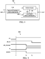
- FIG. 1 illustrates an example of a system 100 to smooth a transition from a low power mode to a high power mode of the system 100.
- the system 100 is a switching power supply (SMPS).
- the system 100 includes a power stages 116 element coupled to a system output VOUT and a feedback loop 120, a low power mode controller 118 coupled to the power stages 116 and VOUT, and a simulated feedback error generator 114 coupled to the feedback loop 120.
- the feedback loop 120 is further coupled to the low power mode controller 118.
- the system 100 converts an input direct current (DC) voltage to a proper output DC voltage available at VOUT.
- the system 100 modifies a duty cycle to arrive at such a target output DC voltage at VOUT.
- Such a voltage at VOUT can be maintained by the system 100 to substantially match a target predesigned voltage.
- the system 100 maintains a target predesigned current at VOUT by modifying the duty cycle.
- the system 100 operates in a low power mode and a high power mode, and additionally operates during a transition period between the low power mode and the high power mode. During the low power mode, much of the system 100 is disabled, with the remaining components of the system 100 producing a smaller amount of power than is available during the high power mode, described in more detail with reference to FIG. 2 .
- the entire system 100 is activated to produce the target output DC voltage VOUT.
- the system 100 determines and applies a simulated feedback error signal to allow the system 100 to begin the high power mode producing a voltage that meets target voltage requirements at VOUT, substantially mitigating conventional time needed to settle at the target predesigned voltage VOUT for the system 100, thereby substantially mitigating overshoot and undershoot at VOUT that conventionally occurs after change to the high power mode.
- the simulated feedback error generator 114 produces a simulated voltage error amplitude (VEA) signal that represents an amount of voltage error that exists at VOUT.
- the simulated feedback error generator 114 produces a simulated current error amplitude (CEA) signal that represents an amount of current error that exists at VOUT.
- the VEA signal and CEA signal produce a forced balanced state within system 100 to give the feedback loop 120 a proper starting point(s) with which to being the high power mode.
- the low power mode controller 118 of the system 100 activates transition from the low power mode to the high power mode, the system 100 begins the transition period.
- the simulated feedback error generator 114 determines the simulated VEA signal and applies such a signal to the feedback loop 120 before a VOUT being produced by the system 100 in the high power mode.
- the feedback loop 120 has a beginning error signal applied during the transition period before any error even exists at VOUT, with such a beginning error signal setting the feedback loop 120 to produce a target VOUT. Then, during the transition of the system 100 to the high power mode, the simulated feedback error generator 114 is disabled and the normal feedback functions of the feedback loop 120 take over to maintain the target VOUT.
- the simulated feedback error generator 114 accounts for variables within the system 100 that cannot be conventionally accounted for. For example, the simulated feedback error generator 114 accounts for variations in power, voltage, and temperature within the system 100 that results in changes to the simulated voltage error amplitude (VEA) signal and the simulated current error amplitude (CEA) signal. Likewise, the simulated feedback error generator 114 accounts for variations in switching frequencies of a particular modulator being employed within the system 100, manufacturing variations for the components within the system 100, variations in various input voltages VREF, VIN, VDD, etc.. The simulated feedback error generator 114 accounts for any variations within the system 100 that results in changes to the simulated VEA signal and the simulated CEA signal that results in the system 100 beginning the high power mode with substantially zero error in the feedback loop 120.
- the power stages 116 produces power for the system 100 during the low power mode and the high power mode. Such a low power mode requires less power at VOUT than is required during the high power mode.
- the power stages 116 is modulated with a signal having a duty cycle that allows the power stages 116 to maintain a target power at VOUT during the low power mode.
- the low power mode controller 118 provides such a modulated signal to the power stages 116. When the system 100 transitions from the low power mode to the high power mode, the low power mode controller 118 activates the power stages 116 to allow the system 100 to produce high power at VOUT.
- the low power mode controller 118 receives a voltage signal from VOUT during the low power mode to allow the low power mode controller 118 to modify a duty cycle used to produce a voltage at VOUT during the low power mode. In one example, the low power mode controller 118 receives a current signal from VOUT during the low power mode to allow the low power mode controller 118 to modify a duty cycle used to produce a current at VOUT during the low power mode.
- the system 100 can be employed as a power supply to supply power to electronics of an automobile.
- the system 100 operates in a low power mode when the automobile is parked with the ignition off and a high power mode when the ignition is turned on and most of the automobile's electronics are active.
- the electronics transition from this low power mode to the high power mode.
- conventionally such a change requires time for the system 100 to settle at a predesignated target voltage and current.
- the example system 100 substantially mitigates such delays when making the transition from an automobile's low power mode to the high power mode.
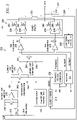
- FIG. 2 illustrates an example circuit 200 to smooth a transition from a low power mode to a high power mode of the circuit 200.
- the term circuit can include a collection of active and/or passive elements that perform a circuit function, such as an amplifier and a comparator. Also, for example, the term circuit can include an integrated circuit where all the circuit elements are fabricated on a common substrate.
- the circuit 200 accepts a reference voltage VREF as an input to a voltage loop amplifier 216.
- the voltage loop amplifier 216 produces a voltage error amplitude (VEA) signal that represents an amount of voltage error within the voltage loop 240.
- VOA voltage error amplitude
- the voltage loop amplifier 216 has a switch S2 coupled across its two input terminals.
- a switch S1 is coupled to the input terminal of the voltage loop amplifier 216 opposite the VREF input.
- the switch S1 is coupled to the voltage feedback loop 240 between resistor 212 and resistor 214, the resistor 212 and resistor 214 forming a voltage divider.
- An output of the voltage loop amplifier 216 is coupled to a voltage clamp 222 that clamps an output voltage of the voltage loop amplifier 216 between a Vmin which is a minimum reference voltage at the output of the voltage loop amplifier 216 and a Vmax which is a maximum reference voltage at the output of the voltage loop amplifier 216.
- Capacitor 244 is coupled to resistor 242 which is coupled to the output of the voltage loop amplifier 216, the capacitor 244 and resistor 242 providing voltage loop compensation.
- a current loop amplifier 220 is coupled to the output of the voltage loop amplifier 216.
- the current loop amplifier 220 produces a current error amplitude (CEA) signal that represents an amount of current error within the current loop 248.
- CEA current error amplitude
- the current loop amplifier has a switch coupled across its two input terminals. One terminal of the current loop amplifier 220 is coupled to the output of the voltage loop amplifier 216 and the other terminal of the current loop amplifier 220 is coupled to the current sense 218 within the current feedback loop 248.
- the current sense 218 is additionally coupled to the precharge voltage generator 238.
- a capacitor 246 is coupled to a resistor 250, with the resistor 250 being coupled to an output of the current loop amplifier 220, such that the capacitor 246 and resistor 250 provide current loop compensation.
- a capacitor 232 is coupled to VOUT.
- the feedback loop 120 shown in FIG. 1 may include the voltage feedback loop 240, the current feedback loop 248, or both the voltage feedback loop 240 and the current feedback loop 248.
- a pulse-width modulation (PWM) modulator 224 is coupled to and provides a buck ramp modulated signal to PWM comparator 226 and boost ramp modulated signal to PWM comparator 228.
- the ramp generator 224 produces a sawtooth wave signal.
- the PWM comparators 226 and 228 are coupled to the output of the current loop amplifier 220.
- the precharge voltage generator 238 is coupled to the output of the current loop amplifier 220.
- the current loop amplifier 220 outputs an error signal to the PWM comparators 226 and 228, with such an error signal setting the duty cycle of the circuit 200 to produce a target voltage and target current at VOUT.
- the precharge voltage generator 238 and the ramp generator 224 are coupled to an input voltage VDD.
- the outputs of the PWM comparators 226 and 228 are coupled to a power stages 236 circuit element, with the output of power stages 236 producing a target voltage and current at VOUT in both the high power mode and the low power mode.
- An inductor 252 is coupled across first and second stages of the power stages 236.
- the power stages 236 transitions the circuit 200 from the low power mode to the high power mode, producing target voltage and current in the low power mode via modulated signals temporarily received from the low power mode controller 230 during the low power mode.
- the power stages 236 is driven by a pulse voltage produced by the PWM comparators 226 and 228 and makes corresponding voltage available at VOUT.
- the precharge voltage generator 238, the ramp generator 224, and the power stages 236 are coupled to an input voltage VIN, with power from VIN being sent to VOUT.
- the power stages 236 includes a first stage and a second stage.
- the first stage of the power stages 236 includes a buffer element 258 and an inverter 260 in parallel, both coupled to the output of the PWM comparator 226.
- An output of the buffer element 258 and inverter 260 are coupled to field-effect transistors (FETs) 262 and 264, respectively.
- the FETs 262 and 264 are coupled to inductor 252.
- the second stage of the power stages 236 includes a buffer element 254 and an inverter 256 in parallel, both coupled to the output of the PWM comparator 228.
- An output of the buffer element 254 and inverter 256 are coupled to FETs 266 and 268, respectively.
- the FET 266 is further coupled to VOUT and the current feedback loop 248, with FET 268 being coupled to inductor 252 and current feedback loop 248.
- the power stages 236 supports both a buck mode and a boost mode, with the VIN being either lower or higher than output voltage VOUT.
- elements 228, 254, 256, 266, and 268 are not activated by the example circuit 200
- elements 226, 258, 260, 262, and 264 are not activated by the example circuit 200.
- the low power mode controller 230 includes a modulator that operates in the low power mode to set a duty cycle of the power stages 236. Such a duty cycle in the low power mode is based on feedback that the low power mode controller 230 receives from VOUT.
- switches S1 are open and switches S2,S3 and S4 are closed. Closing switches S2 and S3 during the low power mode shorts the inputs of the loop amplifiers 216 and 220, respectively. Such shorting provides the benefit of establishing a balanced state for the loop amplifiers 216 and 220 when the loop amplifiers 216 and 220 begin being employed in the high power mode.
- switches S2 and S3 are opened to allow the voltage loop 240 and the current loop 248 to maintain the proper voltage and current at VOUT, respectively.
- Opening switch S1 prevents a voltage from the voltage loop 240 from being applied to the voltage loop amplifier 216 during the low power mode. Opening switch S4 prevents the precharge voltage generator 238 from applying a precharge voltage, PRECHARGE, to the output of the current loop amplifier 220 during the high power mode. During the transition period between the low power mode and the high power mode of the circuit 200, the switch S4 is closed. Closing of switch S4 enables the precharge voltage generator 238 to apply a simulated voltage feedback error signal at the output of the current loop amplifier. Such a simulated voltage feedback error signal sets the starting duty cycle for the PWM comparators 226 and 228 as changing from the transition period to the high power mode.
- the circuit 200 begins the high power mode by powering on components of the circuit 200 that were powered off during the low power mode and begin producing a voltage, based on the precharge voltage produced by the precharge voltage generator 238, at VOUT with substantially zero error and matching a target voltage for VOUT.
- the circuit 200 employs the current sense 218 within the current loop 248 to perform a function similar to that described for the precharge voltage generator 238, except to apply a simulated current feedback error signal, CSENSE voltage.
- the current sense 218 and the output of the voltage loop amplifier 220, VEA are clamped to a common mode voltage.
- Such a simulated current feedback error signal sets the starting duty cycle for the PWM comparators 226 and 228 as changing from the transition period to the high power mode.
- the circuit 200 begins the high power mode by powering on components of the circuit 200 that were powered off during the low power mode and begin producing a current, based on the CSENSE voltage produced by the current sense 218, at VOUT with substantially zero error matching a target current for VOUT, substantially mitigating time needed for the circuit to settle at the target current for VOUT.
- the precharge voltage generator 238 may be employed without assistance from the current sense 218.
- the current sense 218 may be employed without assistance from the precharge voltage generator 238.
- the current sense 218 and the precharge voltage generator 238 may both be employed.
- the precharge voltage generator 238 may operate with less transition accuracy on VOUT when the circuit 200 lacks the current sense 218 driving voltage loop amplifier 220.
- the current sense 218 drives the voltage loop amplifier 220 to operate the current loop.
- the voltage produced by the precharge voltage generator 238 and the ramp generator 224 is independent of VDD, where variations to VDD will not affect VOUT, and the same being true for Fsw, process, and Temperature.
- a default Temperature can used to determine the precharge voltage, with the default Temperature for the circuit 200 being used when the circuit 200 is below a threshold temperature.
- V PWM_RAMP is either the buck ramp voltage (BU RAMP) or the boost ramp voltage (BO_RAMP) produced by the ramp generator 224.
- power stages 236 is driven by one of the PWM comparators 226 and 228 associated with such modes.
- Ramp Gain tracks frequency of switching, resistance and capacitance for a buck regulator of the ramp generator 224, instead of using a fixed gain, generated using a replica of a ramp generator.
- k1 is set to an appropriate value so that the voltage produced by the precharge voltage generator 238 is a little higher, such that the duty cycle is a little higher to compensate at VOUT for any voltage loss that occurs in the power stages 236.
- FET field-effect transistor
- k1 ⁇ R ⁇ I CSENSE tracks a resistance, RDSON, of FET 266 to calculate the proper CEA voltage dependent on whether a light or heavy load is attached to the circuit 200.
- the output of the current sense 218 is coupled to the precharge voltage generator 238 as a basis of calculating Equation 4.
- V REF ⁇ k 2 is ideal VOUT target voltage
- V DROP is voltage loss due to power stages resistances
- VOUT V REF ⁇ k 2 Accordingly, VOUT is at expected value during transition.
- FIG. 3 illustrates an example timing diagram 300 of the circuit 200 shown in FIG. 2 .
- the timing diagram 300 illustrates logic transitions for an enable signal "EN”, a low power mode enable signal “LPM EN”, a low power mode release signal “LPM RELEASE”, a switching signal for switch S1, and a switching signal for switches S2, S3, and S4.
- LPM RELEASE goes low when all of the voltages VEA, CSENSE, and CEA voltages settle at their target values. Also at T2, switches S1 is closed and switches S2, S3, and S4 are opened to place the circuit 200 in the high power mode.
- the current loop 248 and the voltage loop 240 take over control of maintaining the power at VOUT at a target voltage and a target current level.
- LPM EN goes low to disable the low power mode of the circuit 200, which disables the precharge voltage generator 238 and low power mode controller 230.
- the circuit 200 completes the transition period and operates in the high power mode.
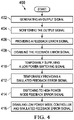
- FIG. 4 a method in accordance with various aspects of example embodiments is described with reference to FIG. 4 .
- the method of FIG. 4 is shown and described as executing serially, but example embodiments are not limited by the illustrated order, as some aspects could occur in different orders and/or concurrently with other aspects from that shown and described herein.
- not all illustrated features may be required to implement a method in accordance with an aspect of example embodiments.
- the method of FIG. 4 can include additional functional features (even if not described herein), with FIG. 4 being described with reference to the examples illustrated herein.
- FIG. 4 illustrates an example of a method 400 for smoothing a transition from a low power mode to a high power mode of the system 100 and circuit 200 shown in FIGS. 1 and 2 .
- the method 400 provides an output signal.
- the power stages 116 and 236 provide the output signal in response to a switching signal.
- the power stages 116 and 236 receive the switching signal from the low power mode controller 118 and 230.
- the method 400 monitors the output signal.
- the output signal, a voltage and/or current at VOUT is monitored with the feedback loop 120.
- the feedback loop 120 may include the voltage feedback loop 240, the current feedback loop 248, or both the voltage feedback loop 240 and the current feedback loop 248.
- the method 400 provides a feedback error signal.
- the feedback loop 120 provides a feedback error signal that is employed to adjust a duty cycle to regulate the output signal, VOUT.
- the feedback error signal includes at least one of a voltage feedback error representing an amount of error in the voltage available at VOUT, and a current feedback error representing an amount of error in the current being produced at VOUT during the high power mode.
- the method 400 disables the feedback loop 120.
- the low power mode controller 118 disables the feedback loops 120, 240, and 248 during a low power mode. Accordingly, the feedback error signal produced by the feedback loops 120, 240, and 248 is disabled in the low power mode.
- the method 400 temporarily supplies a switching signal.
- the low power mode controller 118 and 230 temporarily supply the switching signal to the power stages 116 during the low power mode.
- the method 400 temporarily provides the simulated feedback error signal.
- the simulated feedback error generator 114, current sense 218, and precharge voltage generator 238 provide a simulated feedback error signal to a switching power supply during a transition period from the low power mode, wherein the low power mode controller 118 enables the simulated feedback error generator 114, current sense 218, and precharge voltage generator 238 during the transition period until circuitry associated with the feedback error signal has transitioned back into providing the feedback error signal.
- the method 400 switches to producing the feedback error signal.
- the current loop amplifier 220 is activated to produce a feedback error signal.
- the method 400 disables the low power mode controller 118 and the simulated feedback error signal produced by the simulated feedback error generator 114, current sense 218, and precharge voltage generator 238.
Landscapes
- Engineering & Computer Science (AREA)
- Power Engineering (AREA)
- Dc-Dc Converters (AREA)
Applications Claiming Priority (2)
| Application Number | Priority Date | Filing Date | Title |
|---|---|---|---|
| US15/296,839 US10014774B2 (en) | 2016-10-18 | 2016-10-18 | Power supply with low to high power transition mode |
| PCT/US2017/057263 WO2018075687A1 (en) | 2016-10-18 | 2017-10-18 | Power supply with low to high power transition mode |
Publications (3)
| Publication Number | Publication Date |
|---|---|
| EP3529884A1 EP3529884A1 (en) | 2019-08-28 |
| EP3529884A4 EP3529884A4 (en) | 2019-10-09 |
| EP3529884B1 true EP3529884B1 (en) | 2022-11-02 |
Family
ID=61904160
Family Applications (1)
| Application Number | Title | Priority Date | Filing Date |
|---|---|---|---|
| EP17862982.0A Active EP3529884B1 (en) | 2016-10-18 | 2017-10-18 | Power supply with low to high power transition mode |
Country Status (5)
| Country | Link |
|---|---|
| US (1) | US10014774B2 (cg-RX-API-DMAC7.html) |
| EP (1) | EP3529884B1 (cg-RX-API-DMAC7.html) |
| JP (2) | JP7060851B2 (cg-RX-API-DMAC7.html) |
| KR (1) | KR102524950B1 (cg-RX-API-DMAC7.html) |
| WO (1) | WO2018075687A1 (cg-RX-API-DMAC7.html) |
Families Citing this family (4)
| Publication number | Priority date | Publication date | Assignee | Title |
|---|---|---|---|---|
| US10320292B2 (en) * | 2016-12-27 | 2019-06-11 | Rohm Co., Ltd. | Phase compensation circuit and DC/DC converter using the same |
| US10491116B2 (en) * | 2017-02-09 | 2019-11-26 | Microchip Technology Incorporated | Fast transient response circuit |
| US12113429B1 (en) | 2022-03-24 | 2024-10-08 | Cirrus Logic Inc. | Smooth transition between power modes in a power converter |
| US12381469B2 (en) | 2022-08-17 | 2025-08-05 | Cirrus Logic Inc. | Pulse frequency modulation regulation and exit scheme using single comparator for power converter |
Family Cites Families (15)
| Publication number | Priority date | Publication date | Assignee | Title |
|---|---|---|---|---|
| JPH09215320A (ja) | 1996-01-30 | 1997-08-15 | Hitachi Ltd | 自動車制御装置用電源回路 |
| WO2007024675A1 (en) * | 2005-08-23 | 2007-03-01 | Analog Devices, Inc. | Improving transient behavior while switching between control loops in a switching voltage regulator |
| CN1992493B (zh) | 2005-12-30 | 2011-05-18 | 艾默生网络能源系统北美公司 | 一种谐振直流/直流变换器及其控制方法 |
| US7990119B2 (en) * | 2008-07-29 | 2011-08-02 | Telefonaktiebolaget L M Ericsson (Publ) | Multimode voltage regulator circuit |
| TWI368838B (en) * | 2008-09-02 | 2012-07-21 | Richtek Technology Corp | Buck switching regulator with improved mode transition and control method thereof |
| DK177105B1 (en) * | 2009-08-14 | 2011-09-05 | Zzzero Aps | Low power switch mode power supply and use of the power supply |
| JP5586211B2 (ja) * | 2009-11-17 | 2014-09-10 | 株式会社東芝 | Dc−dcコンバータおよび半導体集積回路 |
| US8912773B2 (en) * | 2011-01-20 | 2014-12-16 | International Rectifier Corporation | Synchronous buck converter including multi-mode control for light load efficiency and related method |
| US8994351B2 (en) | 2011-08-02 | 2015-03-31 | Power Integrations, Inc. | Smooth mode transition plateau for a power supply controller |
| JP5844106B2 (ja) * | 2011-09-28 | 2016-01-13 | 三洋電機株式会社 | 車両用の電源装置とこの電源装置を備える車両 |
| JP6154584B2 (ja) * | 2012-06-18 | 2017-06-28 | ローム株式会社 | 電源装置、並びに、これを用いた車載機器及び車両 |
| CN103973267B (zh) * | 2013-01-25 | 2018-04-10 | 恩智浦美国有限公司 | 具有电源模式控制缓冲器的电子器件 |
| JP6097237B2 (ja) * | 2014-03-10 | 2017-03-15 | 株式会社東芝 | Dc−dcコンバータおよび半導体集積回路 |
| CN104767372B (zh) * | 2015-04-24 | 2017-12-19 | 矽力杰半导体技术(杭州)有限公司 | 控制电路、控制方法和应用其的反激式变换器 |
| JP2016106521A (ja) * | 2016-03-16 | 2016-06-16 | ルネサスエレクトロニクス株式会社 | デジタル制御電源装置 |
-
2016
- 2016-10-18 US US15/296,839 patent/US10014774B2/en active Active
-
2017
- 2017-10-18 JP JP2019520828A patent/JP7060851B2/ja active Active
- 2017-10-18 EP EP17862982.0A patent/EP3529884B1/en active Active
- 2017-10-18 KR KR1020197010749A patent/KR102524950B1/ko active Active
- 2017-10-18 WO PCT/US2017/057263 patent/WO2018075687A1/en not_active Ceased
-
2022
- 2022-03-30 JP JP2022055363A patent/JP7293445B2/ja active Active
Also Published As
| Publication number | Publication date |
|---|---|
| JP7060851B2 (ja) | 2022-04-27 |
| JP7293445B2 (ja) | 2023-06-19 |
| KR102524950B1 (ko) | 2023-05-02 |
| KR20190065295A (ko) | 2019-06-11 |
| US10014774B2 (en) | 2018-07-03 |
| JP2019531690A (ja) | 2019-10-31 |
| WO2018075687A1 (en) | 2018-04-26 |
| US20180109186A1 (en) | 2018-04-19 |
| JP2022088554A (ja) | 2022-06-14 |
| EP3529884A1 (en) | 2019-08-28 |
| EP3529884A4 (en) | 2019-10-09 |
Similar Documents
| Publication | Publication Date | Title |
|---|---|---|
| US12444966B2 (en) | Power management circuit | |
| US10468988B2 (en) | Three-level converter using an auxiliary switched capacitor circuit | |
| CN101610033B (zh) | Dc-dc变换器 | |
| US7804282B2 (en) | Buck converter with inductor pre-energizing | |
| JP7293445B2 (ja) | 低電力から高電力への遷移モードを備える電力供給 | |
| US9385600B2 (en) | Low-loss step-up and step-down voltage converter | |
| US7812585B2 (en) | Advanced current-mode control for switched regulators | |
| US7504812B2 (en) | Transient behavior while switching between control loops in a switching voltage regulator | |
| US20170257026A1 (en) | Voltage converter control circuits and methods | |
| US20090108820A1 (en) | Topology for a positive buck-boost switching regulator | |
| US10020732B2 (en) | Power converter having low power operating mode | |
| US7256570B2 (en) | Light load current-mode control for switched step up-step down regulators | |
| TWI683519B (zh) | 模式控制裝置、電壓轉換器及模式控制方法 | |
| US10454370B2 (en) | Three quarter bridge for buck-derived switch-mode power supplies | |
| US8164315B2 (en) | Power supply circuit | |
| US11233454B2 (en) | Power stages and current monitor output signal (IMON) generation circuit | |
| US20220321004A1 (en) | Current limiting circuit | |
| US9413232B2 (en) | Droop reduction circuit for charge pump buck converter | |
| US20070253229A1 (en) | Startup for DC/DC converters | |
| KR101239628B1 (ko) | 직류-직류 컨버터 | |
| US8198879B2 (en) | Booster circuit and PWM signal generator | |
| EP1198057A2 (en) | A power supply |
Legal Events
| Date | Code | Title | Description |
|---|---|---|---|
| STAA | Information on the status of an ep patent application or granted ep patent |
Free format text: STATUS: THE INTERNATIONAL PUBLICATION HAS BEEN MADE |
|
| PUAI | Public reference made under article 153(3) epc to a published international application that has entered the european phase |
Free format text: ORIGINAL CODE: 0009012 |
|
| STAA | Information on the status of an ep patent application or granted ep patent |
Free format text: STATUS: REQUEST FOR EXAMINATION WAS MADE |
|
| 17P | Request for examination filed |
Effective date: 20190520 |
|
| AK | Designated contracting states |
Kind code of ref document: A1 Designated state(s): AL AT BE BG CH CY CZ DE DK EE ES FI FR GB GR HR HU IE IS IT LI LT LU LV MC MK MT NL NO PL PT RO RS SE SI SK SM TR |
|
| AX | Request for extension of the european patent |
Extension state: BA ME |
|
| A4 | Supplementary search report drawn up and despatched |
Effective date: 20190909 |
|
| RIC1 | Information provided on ipc code assigned before grant |
Ipc: H02M 3/156 20060101AFI20190903BHEP Ipc: H02M 1/00 20060101ALI20190903BHEP Ipc: H02M 3/158 20060101ALI20190903BHEP Ipc: H02M 1/42 20070101ALI20190903BHEP |
|
| DAV | Request for validation of the european patent (deleted) | ||
| DAX | Request for extension of the european patent (deleted) | ||
| STAA | Information on the status of an ep patent application or granted ep patent |
Free format text: STATUS: EXAMINATION IS IN PROGRESS |
|
| 17Q | First examination report despatched |
Effective date: 20200408 |
|
| GRAP | Despatch of communication of intention to grant a patent |
Free format text: ORIGINAL CODE: EPIDOSNIGR1 |
|
| STAA | Information on the status of an ep patent application or granted ep patent |
Free format text: STATUS: GRANT OF PATENT IS INTENDED |
|
| INTG | Intention to grant announced |
Effective date: 20220610 |
|
| GRAS | Grant fee paid |
Free format text: ORIGINAL CODE: EPIDOSNIGR3 |
|
| GRAA | (expected) grant |
Free format text: ORIGINAL CODE: 0009210 |
|
| STAA | Information on the status of an ep patent application or granted ep patent |
Free format text: STATUS: THE PATENT HAS BEEN GRANTED |
|
| AK | Designated contracting states |
Kind code of ref document: B1 Designated state(s): AL AT BE BG CH CY CZ DE DK EE ES FI FR GB GR HR HU IE IS IT LI LT LU LV MC MK MT NL NO PL PT RO RS SE SI SK SM TR |
|
| REG | Reference to a national code |
Ref country code: GB Ref legal event code: FG4D |
|
| REG | Reference to a national code |
Ref country code: CH Ref legal event code: EP Ref country code: AT Ref legal event code: REF Ref document number: 1529505 Country of ref document: AT Kind code of ref document: T Effective date: 20221115 |
|
| REG | Reference to a national code |
Ref country code: DE Ref legal event code: R096 Ref document number: 602017063384 Country of ref document: DE |
|
| REG | Reference to a national code |
Ref country code: IE Ref legal event code: FG4D |
|
| REG | Reference to a national code |
Ref country code: LT Ref legal event code: MG9D |
|
| REG | Reference to a national code |
Ref country code: NL Ref legal event code: MP Effective date: 20221102 |
|
| REG | Reference to a national code |
Ref country code: AT Ref legal event code: MK05 Ref document number: 1529505 Country of ref document: AT Kind code of ref document: T Effective date: 20221102 |
|
| PG25 | Lapsed in a contracting state [announced via postgrant information from national office to epo] |
Ref country code: SE Free format text: LAPSE BECAUSE OF FAILURE TO SUBMIT A TRANSLATION OF THE DESCRIPTION OR TO PAY THE FEE WITHIN THE PRESCRIBED TIME-LIMIT Effective date: 20221102 Ref country code: PT Free format text: LAPSE BECAUSE OF FAILURE TO SUBMIT A TRANSLATION OF THE DESCRIPTION OR TO PAY THE FEE WITHIN THE PRESCRIBED TIME-LIMIT Effective date: 20230302 Ref country code: NO Free format text: LAPSE BECAUSE OF FAILURE TO SUBMIT A TRANSLATION OF THE DESCRIPTION OR TO PAY THE FEE WITHIN THE PRESCRIBED TIME-LIMIT Effective date: 20230202 Ref country code: LT Free format text: LAPSE BECAUSE OF FAILURE TO SUBMIT A TRANSLATION OF THE DESCRIPTION OR TO PAY THE FEE WITHIN THE PRESCRIBED TIME-LIMIT Effective date: 20221102 Ref country code: FI Free format text: LAPSE BECAUSE OF FAILURE TO SUBMIT A TRANSLATION OF THE DESCRIPTION OR TO PAY THE FEE WITHIN THE PRESCRIBED TIME-LIMIT Effective date: 20221102 Ref country code: ES Free format text: LAPSE BECAUSE OF FAILURE TO SUBMIT A TRANSLATION OF THE DESCRIPTION OR TO PAY THE FEE WITHIN THE PRESCRIBED TIME-LIMIT Effective date: 20221102 Ref country code: AT Free format text: LAPSE BECAUSE OF FAILURE TO SUBMIT A TRANSLATION OF THE DESCRIPTION OR TO PAY THE FEE WITHIN THE PRESCRIBED TIME-LIMIT Effective date: 20221102 |
|
| PG25 | Lapsed in a contracting state [announced via postgrant information from national office to epo] |
Ref country code: RS Free format text: LAPSE BECAUSE OF FAILURE TO SUBMIT A TRANSLATION OF THE DESCRIPTION OR TO PAY THE FEE WITHIN THE PRESCRIBED TIME-LIMIT Effective date: 20221102 Ref country code: PL Free format text: LAPSE BECAUSE OF FAILURE TO SUBMIT A TRANSLATION OF THE DESCRIPTION OR TO PAY THE FEE WITHIN THE PRESCRIBED TIME-LIMIT Effective date: 20221102 Ref country code: LV Free format text: LAPSE BECAUSE OF FAILURE TO SUBMIT A TRANSLATION OF THE DESCRIPTION OR TO PAY THE FEE WITHIN THE PRESCRIBED TIME-LIMIT Effective date: 20221102 Ref country code: IS Free format text: LAPSE BECAUSE OF FAILURE TO SUBMIT A TRANSLATION OF THE DESCRIPTION OR TO PAY THE FEE WITHIN THE PRESCRIBED TIME-LIMIT Effective date: 20230302 Ref country code: HR Free format text: LAPSE BECAUSE OF FAILURE TO SUBMIT A TRANSLATION OF THE DESCRIPTION OR TO PAY THE FEE WITHIN THE PRESCRIBED TIME-LIMIT Effective date: 20221102 Ref country code: GR Free format text: LAPSE BECAUSE OF FAILURE TO SUBMIT A TRANSLATION OF THE DESCRIPTION OR TO PAY THE FEE WITHIN THE PRESCRIBED TIME-LIMIT Effective date: 20230203 |
|
| P01 | Opt-out of the competence of the unified patent court (upc) registered |
Effective date: 20230523 |
|
| PG25 | Lapsed in a contracting state [announced via postgrant information from national office to epo] |
Ref country code: NL Free format text: LAPSE BECAUSE OF FAILURE TO SUBMIT A TRANSLATION OF THE DESCRIPTION OR TO PAY THE FEE WITHIN THE PRESCRIBED TIME-LIMIT Effective date: 20221102 |
|
| PG25 | Lapsed in a contracting state [announced via postgrant information from national office to epo] |
Ref country code: SM Free format text: LAPSE BECAUSE OF FAILURE TO SUBMIT A TRANSLATION OF THE DESCRIPTION OR TO PAY THE FEE WITHIN THE PRESCRIBED TIME-LIMIT Effective date: 20221102 Ref country code: RO Free format text: LAPSE BECAUSE OF FAILURE TO SUBMIT A TRANSLATION OF THE DESCRIPTION OR TO PAY THE FEE WITHIN THE PRESCRIBED TIME-LIMIT Effective date: 20221102 Ref country code: EE Free format text: LAPSE BECAUSE OF FAILURE TO SUBMIT A TRANSLATION OF THE DESCRIPTION OR TO PAY THE FEE WITHIN THE PRESCRIBED TIME-LIMIT Effective date: 20221102 Ref country code: DK Free format text: LAPSE BECAUSE OF FAILURE TO SUBMIT A TRANSLATION OF THE DESCRIPTION OR TO PAY THE FEE WITHIN THE PRESCRIBED TIME-LIMIT Effective date: 20221102 Ref country code: CZ Free format text: LAPSE BECAUSE OF FAILURE TO SUBMIT A TRANSLATION OF THE DESCRIPTION OR TO PAY THE FEE WITHIN THE PRESCRIBED TIME-LIMIT Effective date: 20221102 |
|
| REG | Reference to a national code |
Ref country code: DE Ref legal event code: R097 Ref document number: 602017063384 Country of ref document: DE |
|
| PG25 | Lapsed in a contracting state [announced via postgrant information from national office to epo] |
Ref country code: SK Free format text: LAPSE BECAUSE OF FAILURE TO SUBMIT A TRANSLATION OF THE DESCRIPTION OR TO PAY THE FEE WITHIN THE PRESCRIBED TIME-LIMIT Effective date: 20221102 Ref country code: AL Free format text: LAPSE BECAUSE OF FAILURE TO SUBMIT A TRANSLATION OF THE DESCRIPTION OR TO PAY THE FEE WITHIN THE PRESCRIBED TIME-LIMIT Effective date: 20221102 |
|
| PLBE | No opposition filed within time limit |
Free format text: ORIGINAL CODE: 0009261 |
|
| STAA | Information on the status of an ep patent application or granted ep patent |
Free format text: STATUS: NO OPPOSITION FILED WITHIN TIME LIMIT |
|
| 26N | No opposition filed |
Effective date: 20230803 |
|
| PG25 | Lapsed in a contracting state [announced via postgrant information from national office to epo] |
Ref country code: SI Free format text: LAPSE BECAUSE OF FAILURE TO SUBMIT A TRANSLATION OF THE DESCRIPTION OR TO PAY THE FEE WITHIN THE PRESCRIBED TIME-LIMIT Effective date: 20221102 |
|
| PG25 | Lapsed in a contracting state [announced via postgrant information from national office to epo] |
Ref country code: IT Free format text: LAPSE BECAUSE OF FAILURE TO SUBMIT A TRANSLATION OF THE DESCRIPTION OR TO PAY THE FEE WITHIN THE PRESCRIBED TIME-LIMIT Effective date: 20221102 Ref country code: MC Free format text: LAPSE BECAUSE OF FAILURE TO SUBMIT A TRANSLATION OF THE DESCRIPTION OR TO PAY THE FEE WITHIN THE PRESCRIBED TIME-LIMIT Effective date: 20221102 |
|
| REG | Reference to a national code |
Ref country code: CH Ref legal event code: PL |
|
| REG | Reference to a national code |
Ref country code: BE Ref legal event code: MM Effective date: 20231031 |
|
| PG25 | Lapsed in a contracting state [announced via postgrant information from national office to epo] |
Ref country code: LU Free format text: LAPSE BECAUSE OF NON-PAYMENT OF DUE FEES Effective date: 20231018 |
|
| PG25 | Lapsed in a contracting state [announced via postgrant information from national office to epo] |
Ref country code: LU Free format text: LAPSE BECAUSE OF NON-PAYMENT OF DUE FEES Effective date: 20231018 |
|
| PG25 | Lapsed in a contracting state [announced via postgrant information from national office to epo] |
Ref country code: CH Free format text: LAPSE BECAUSE OF NON-PAYMENT OF DUE FEES Effective date: 20231031 |
|
| PG25 | Lapsed in a contracting state [announced via postgrant information from national office to epo] |
Ref country code: CH Free format text: LAPSE BECAUSE OF NON-PAYMENT OF DUE FEES Effective date: 20231031 |
|
| PG25 | Lapsed in a contracting state [announced via postgrant information from national office to epo] |
Ref country code: BE Free format text: LAPSE BECAUSE OF NON-PAYMENT OF DUE FEES Effective date: 20231031 |
|
| PG25 | Lapsed in a contracting state [announced via postgrant information from national office to epo] |
Ref country code: IE Free format text: LAPSE BECAUSE OF NON-PAYMENT OF DUE FEES Effective date: 20231018 |
|
| PG25 | Lapsed in a contracting state [announced via postgrant information from national office to epo] |
Ref country code: IE Free format text: LAPSE BECAUSE OF NON-PAYMENT OF DUE FEES Effective date: 20231018 |
|
| PG25 | Lapsed in a contracting state [announced via postgrant information from national office to epo] |
Ref country code: BG Free format text: LAPSE BECAUSE OF FAILURE TO SUBMIT A TRANSLATION OF THE DESCRIPTION OR TO PAY THE FEE WITHIN THE PRESCRIBED TIME-LIMIT Effective date: 20221102 |
|
| PG25 | Lapsed in a contracting state [announced via postgrant information from national office to epo] |
Ref country code: BG Free format text: LAPSE BECAUSE OF FAILURE TO SUBMIT A TRANSLATION OF THE DESCRIPTION OR TO PAY THE FEE WITHIN THE PRESCRIBED TIME-LIMIT Effective date: 20221102 |
|
| PG25 | Lapsed in a contracting state [announced via postgrant information from national office to epo] |
Ref country code: CY Free format text: LAPSE BECAUSE OF FAILURE TO SUBMIT A TRANSLATION OF THE DESCRIPTION OR TO PAY THE FEE WITHIN THE PRESCRIBED TIME-LIMIT; INVALID AB INITIO Effective date: 20171018 |
|
| PG25 | Lapsed in a contracting state [announced via postgrant information from national office to epo] |
Ref country code: HU Free format text: LAPSE BECAUSE OF FAILURE TO SUBMIT A TRANSLATION OF THE DESCRIPTION OR TO PAY THE FEE WITHIN THE PRESCRIBED TIME-LIMIT; INVALID AB INITIO Effective date: 20171018 |
|
| PGFP | Annual fee paid to national office [announced via postgrant information from national office to epo] |
Ref country code: GB Payment date: 20250923 Year of fee payment: 9 |
|
| PGFP | Annual fee paid to national office [announced via postgrant information from national office to epo] |
Ref country code: FR Payment date: 20250925 Year of fee payment: 9 |
|
| PG25 | Lapsed in a contracting state [announced via postgrant information from national office to epo] |
Ref country code: TR Free format text: LAPSE BECAUSE OF FAILURE TO SUBMIT A TRANSLATION OF THE DESCRIPTION OR TO PAY THE FEE WITHIN THE PRESCRIBED TIME-LIMIT Effective date: 20221102 |
|
| PGFP | Annual fee paid to national office [announced via postgrant information from national office to epo] |
Ref country code: DE Payment date: 20250923 Year of fee payment: 9 |