EP3525282B1 - Signalhandhabungsvorrichtung mit mehreren substratlagen - Google Patents
Signalhandhabungsvorrichtung mit mehreren substratlagen Download PDFInfo
- Publication number
- EP3525282B1 EP3525282B1 EP19153509.5A EP19153509A EP3525282B1 EP 3525282 B1 EP3525282 B1 EP 3525282B1 EP 19153509 A EP19153509 A EP 19153509A EP 3525282 B1 EP3525282 B1 EP 3525282B1
- Authority
- EP
- European Patent Office
- Prior art keywords
- conductors
- substrate
- handling device
- conductive
- signal handling
- Prior art date
- Legal status (The legal status is an assumption and is not a legal conclusion. Google has not performed a legal analysis and makes no representation as to the accuracy of the status listed.)
- Active
Links
Images



Classifications
-
- H—ELECTRICITY
- H01—ELECTRIC ELEMENTS
- H01P—WAVEGUIDES; RESONATORS, LINES, OR OTHER DEVICES OF THE WAVEGUIDE TYPE
- H01P3/00—Waveguides; Transmission lines of the waveguide type
- H01P3/12—Hollow waveguides
- H01P3/121—Hollow waveguides integrated in a substrate
-
- H—ELECTRICITY
- H01—ELECTRIC ELEMENTS
- H01P—WAVEGUIDES; RESONATORS, LINES, OR OTHER DEVICES OF THE WAVEGUIDE TYPE
- H01P5/00—Coupling devices of the waveguide type
- H01P5/02—Coupling devices of the waveguide type with invariable factor of coupling
- H01P5/022—Transitions between lines of the same kind and shape, but with different dimensions
- H01P5/024—Transitions between lines of the same kind and shape, but with different dimensions between hollow waveguides
-
- H—ELECTRICITY
- H01—ELECTRIC ELEMENTS
- H01P—WAVEGUIDES; RESONATORS, LINES, OR OTHER DEVICES OF THE WAVEGUIDE TYPE
- H01P3/00—Waveguides; Transmission lines of the waveguide type
- H01P3/18—Waveguides; Transmission lines of the waveguide type built-up from several layers to increase operating surface, i.e. alternately conductive and dielectric layers
-
- H—ELECTRICITY
- H01—ELECTRIC ELEMENTS
- H01P—WAVEGUIDES; RESONATORS, LINES, OR OTHER DEVICES OF THE WAVEGUIDE TYPE
- H01P5/00—Coupling devices of the waveguide type
- H01P5/08—Coupling devices of the waveguide type for linking dissimilar lines or devices
-
- H—ELECTRICITY
- H05—ELECTRIC TECHNIQUES NOT OTHERWISE PROVIDED FOR
- H05K—PRINTED CIRCUITS; CASINGS OR CONSTRUCTIONAL DETAILS OF ELECTRIC APPARATUS; MANUFACTURE OF ASSEMBLAGES OF ELECTRICAL COMPONENTS
- H05K1/00—Printed circuits
- H05K1/02—Details
- H05K1/0213—Electrical arrangements not otherwise provided for
- H05K1/0237—High frequency adaptations
- H05K1/0242—Structural details of individual signal conductors, e.g. related to the skin effect
-
- H—ELECTRICITY
- H05—ELECTRIC TECHNIQUES NOT OTHERWISE PROVIDED FOR
- H05K—PRINTED CIRCUITS; CASINGS OR CONSTRUCTIONAL DETAILS OF ELECTRIC APPARATUS; MANUFACTURE OF ASSEMBLAGES OF ELECTRICAL COMPONENTS
- H05K1/00—Printed circuits
- H05K1/02—Details
- H05K1/0213—Electrical arrangements not otherwise provided for
- H05K1/0237—High frequency adaptations
- H05K1/025—Impedance arrangements, e.g. impedance matching, reduction of parasitic impedance
- H05K1/0251—Impedance arrangements, e.g. impedance matching, reduction of parasitic impedance related to vias or transitions between vias and transmission lines
-
- H—ELECTRICITY
- H05—ELECTRIC TECHNIQUES NOT OTHERWISE PROVIDED FOR
- H05K—PRINTED CIRCUITS; CASINGS OR CONSTRUCTIONAL DETAILS OF ELECTRIC APPARATUS; MANUFACTURE OF ASSEMBLAGES OF ELECTRICAL COMPONENTS
- H05K1/00—Printed circuits
- H05K1/02—Details
- H05K1/11—Printed elements for providing electric connections to or between printed circuits
- H05K1/115—Via connections; Lands around holes or via connections
Definitions
- radar systems and wireless communication systems include over-the-air signaling.
- One challenge associated with such systems is providing adequate bandwidth in devices that handle such signals.
- Some existing signal handling devices include a transition from a substrate integrated waveguide to an orthogonally oriented, air-filled waveguide.
- the bandwidth of such devices is typically very narrow resulting in poor manufacturability.
- One attempt at increasing the bandwidth for such devices has been to include metal plates to establish a resonating cavity. Such plates have to be particularly designed for particular applications, which introduces manufacturing inefficiencies. Additionally, such plates increase the cost of the device.
- a signal handling device in accordance with the preamble of claim 1 is substantially known from US 2008 / 309 427 A1 . Further details of signal handling devices are disclosed in references JP 2004 135 095 A , EP 2 426 782 A1 and EP 1 195 839 A1 .
- a signal handling device comprising all the features of present claim 1.
- the first substrate comprises a dielectric material
- the first conductors comprise vias
- the second substrate comprises a dielectric material
- the second conductors comprise vias
- the signal carrier comprises a waveguide
- the waveguide comprises an air-filled waveguide.
- the first substrate is planar
- the second substrate is planar and parallel with the first substrate
- the signal carrier is at least partially transverse to the first substrate.
- the signal carrier is at least partially perpendicular to the first substrate.
- An example embodiment having one or more features of the signal handling device of any of the previous paragraphs includes a pressure sensitive adhesive aligned with one side of the first substrate and wherein at least a portion of one end of the signal carrier is secured to the pressure sensitive adhesive.
- the conductive ribbon establishes a barrier to prevent signal leakage from the second conductors through the adhesive layer.
- the conductive ribbon establishes a frame corresponding to a perimeter of the resonating cavity formed by the second conductors and the conductive ribbon has an opening aligned with the first and second openings.
- the adhesive in contact with the second conductive layer comprises a fibrous material impregnated with a resin.
- each of the conductive layers comprises metal.
- the first opening is generally rectangular, the first opening has four sides, three sides of the first opening are bordered by at least some of the first conductors, the second opening is generally rectangular, and the second opening is surrounded by at least some of the second conductors.
- the at least some of the first conductors that border the three sides of the first opening are coaxial with respective ones of the at least some of the second conductors.
- others of the first conductors are arranged in two parallel lines and the others of the first conductors establish a fence of the substrate integrated waveguide.
- a signal handling device designed according to an embodiment of this invention includes a resonating cavity formed by conductors in a dielectric substrate that facilitates propagating an electromagnetic wave from a substrate integrated waveguide to a transversely oriented waveguide.
- Embodiments of this invention increase bandwidth compared to previous devices that include a transition from a substrate integrated waveguide to an air-filled waveguide. For example, some embodiments provide up to four times the bandwidth available with previous signal handling devices.
- Figures 1 and 2 diagrammatically illustrate a signal handling device 20 that may be used for a variety of purposes.
- One example use includes signal handling for devices mounted on an automotive vehicle. Some implementations are useful for automated vehicles that have autonomous or semi-autonomous vehicle control features. Another useful implementation of an embodiment of this invention is for wireless communications.
- the example signal handling device 20 includes a first substrate 22 that comprises a dielectric material that is not conductive.
- the first substrate 22 includes a plurality of first conductors 24 that are arranged to form a substrate integrated waveguide.
- a second substrate 26 comprises a dielectric material that is not conductive.
- the second substrate 26 includes a plurality of second conductors 28 that are arranged to form a resonating cavity or backshort near one end of the substrate integrated waveguide.
- An air-filled waveguide 30 is oriented at least partially transverse to the first substrate 22.
- the air-filled waveguide 30 is oriented perpendicular to the first substrate 22.
- a pressure sensitive adhesive layer 36 which is not conductive, facilitates securing the waveguide 30 to the first substrate 22.
- the device 20 includes features that facilitate handling signals, such as electromagnetic waves, that propagate in the substrate integrated waveguide formed by the first conductors 24 and are converted to electromagnetic waves that propagate in the air-filled waveguide 30.
- the first substrate 22 includes a conductive layer 32 on one side of the first substrate 22.
- Another conductive layer 34 is situated on an opposite side of the first substrate 22.
- the conductive layers 32 and 34 in this example comprises a sheet or layer of conductive metal such as copper.
- the conductive layers 32 and 34 respectively contact the ends of the first conductors 24.
- An adhesive layer 40 secures the second substrate 26 to the conductive layer 34 of the first substrate 22.
- the adhesive layer 40 in the illustrated example embodiment comprises a nonconductive prepreg layer including a fibrous material impregnated with a resin.
- a conductive layer 42 is situated on one side of the second substrate 26. The conductive layer 42 contacts one end of the second conductors 28 and provides a cap over the resonating cavity 50 established by the second conductors 28.
- Another conductive layer 44 is situated along a portion of an opposite side of the conductors 28 facing the first substrate 22.
- the conductive layer 44 in this example comprises a ribbon of conductive metal, such as copper, that prevents electromagnetic leakage from the second conductors 28 into and through the adhesive layer 40.
- the illustrated arrangement utilizes a substrate integrated waveguide formed by the first conductors 24 in the first substrate 22 and a backshort or resonating cavity formed by the second conductors 28 in the second substrate 26.
- the resonating cavity 50 is aligned with the air-filled waveguide 30 of the device 20. That alignment facilitates converting an electromagnetic wave propagating through the substrate integrated waveguide into an electromagnetic wave propagating through the air-filled waveguide 30.
- Figure 3 illustrates an example conductive layer 32, such as a sheet of copper.
- the conductive layer 32 includes an opening 52 that is aligned with the waveguide 30 in the fully assembled device 20.
- the opening 52 may be established, for example, by etching away a corresponding area of the conductive layer 32.
- the illustrated example opening 52 includes tabs 54 that are dimensioned to provide microwave matching structures.
- the dimensions of the opening 52 and the tabs 54 may be selected or tuned to control the coupling between the substrate integrated waveguide of the first substrate 22 and the waveguide 30.
- the dimensions or configuration of the opening 52 may also serve as a secondary adjustment of frequency.
- Figure 4 illustrates the first substrate 22 on top of the conductive layer 32.
- the first substrate 22 comprises a dielectric layer and the first conductors 24 comprise vias in the first substrate 22.
- the first conductors 24 are open or empty vias while in other embodiments the vias are at least partially filled with a conductive material.
- one end of the substrate integrated waveguide formed by the first conductors 24 is aligned with the opening 52 to facilitate converting an electromagnetic wave propagating in the substrate integrated waveguide to an electromagnetic wave that propagates in the air-filled waveguide 30.
- Some of the first conductors 24 border three of the four sides of the opening 52 in this example.
- the fourth side of the opening 52 faces toward the port of the substrate integrated waveguide.
- Figure 5 shows the conductive layer 34 on an opposite side of the substrate 22 from the conductive layer 32.
- the conductive layer 34 includes an opening 58 aligned with the opening 52 of the conductive layer 32.
- the conductive layer 34 comprises a sheet of metal, such as copper and the opening 58 is established by etching away a corresponding portion of the layer 34.
- FIG 6 shows the adhesive layer 40 against the conductive layer 34.
- the conductive ribbon 44 is shown in contact with the adhesive layer 40.
- the conductive ribbon 44 in this example has the configuration of a rectangular frame that surrounds the area of the adhesive layer 40 that is aligned with the openings 52 and 58.
- the conductive ribbon 44 in some embodiments comprises a thin layer of copper.
- the conductive ribbon 44 functions as a cap for one side or end of the second conductors 28.
- the dimensions of the conductive ribbon 44 are selected to act as a band-stop filter to minimize or eliminate electromagnetic energy leakage into and through the nonconductive adhesive layer 40. Those skilled in the art who have the benefit of this description will be able to select a ribbon configuration and dimensions to meet their particular needs.
- Figure 7 shows the second substrate 26 situated on the adhesive layer 40.
- the second conductors 28 establish a border around the resonating cavity 50 that facilitates converting an electromagnetic wave propagating through the substrate integrated waveguide of the first substrate 22 into an electromagnetic wave propagating through the air-filled waveguide 30.
- the second conductors 28 comprise vias in the second substrate 26.
- the vias are empty or hollow while in others they are at least partially filled with a conductive material.
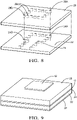
- Figure 8 illustrates the positional relationship among the conductors 28 and 24.
- the second conductors 28 that border the area aligned with the opening 52 are aligned with some of the first conductors 24 that border some of the opening 52.
- Those first conductors 24 are coaxial with corresponding ones of the second conductors 28.
- the first conductors 24a and 24b are respectively coaxially aligned with the second conductors 28a and 28b.
- the alignment of conductors can also be appreciated from Figures 1 and 2 . Others of the first conductors 24 that establish the fence of the substrate integrated waveguide in the substrate 22 are not aligned with second conductors 28 in the second substrate 26.
- One feature of the illustrated example is that the conductors 24 and 28 of the respective substrate layers do not have to be directly connected to each other. This provides a more economical manufacturing process and reduces overall cost. Securing the substrates 22 and 26 together using the adhesive 40 makes the manufacturing process for making the device 20 economical.
- the conductive ribbon 44 aligned with the second conductors 28 provides a cap to prevent leakage into or through the adhesive layer 40.
- Figure 9 shows a conductive layer 42 adjacent the second substrate 26 covering the second conductors 28 on a side of the second substrate 26 that is situated opposite the conductive ribbon 44 and facing away from the first substrate 22.
- the conductive layer 42 in some examples comprises a sheet of copper or another conductive metal.
- the second conductors 28 and the conductive layer 42 provide the backshort of the resonating cavity 50.
- the second substrate layer 26 in some examples includes a thickness that is selected to be approximately one-quarter of the wavelength of a signal frequency of interest in a system into which the signal handling device 20 will be incorporated. Such a substrate thickness is also appropriate for high efficiency antennas such that the device 20 lends itself to highly integrated packaging.
- Figure 10 illustrates another example embodiment that includes the additional feature of an antenna layer 70 on the second substrate 26 near the opening or port of the substrate integrated waveguide.
- Using the second conductors 28 and the second substrate 26 to form the resonating cavity or backshort of the device 20 provides a very wideband transition between the substrate integrated waveguide of the first substrate 22 and the air-filled waveguide 30. This is a significant advantage compared to other signal handling devices that have relatively poor bandwidth characteristics. Some embodiments designed consistent with the illustrated example provide a four-fold increase in bandwidth compared to prior devices.
Landscapes
- Engineering & Computer Science (AREA)
- Microelectronics & Electronic Packaging (AREA)
- Waveguides (AREA)
- Structure Of Printed Boards (AREA)
Claims (11)
- Signalhandhabungsvorrichtung (20), die umfasst:ein erstes Substrat (22);eine Vielzahl von ersten Leitern (24) in dem ersten Substrat (22), wobei die ersten Leiter (24) so angeordnet sind, dass sie einen in das Substrat integrierten Wellenleiter bilden;ein zweites Substrat (26);eine Vielzahl von zweiten Leitern (28) in dem zweiten Substrat (26), wobei die zweiten Leiter (28) so angeordnet sind, dass sie einen Resonanzhohlraum (50) in der Nähe eines Endes des in das Substrat integrierten Wellenleiters bilden; undeinen Signalträger (30), der mit dem einen Ende des in das Substrat integrierten Wellenleiters ausgerichtet ist; wobeidie Signalhandhabungsvorrichtung (20) ferner umfasst:eine erste leitende Schicht (32) an einer Seite des ersten Substrats (22), wobei die erste leitende Schicht (32) in leitendem Kontakt mit den ersten Leitern (24) steht, wobei die erste leitende Schicht (32) eine erste Öffnung (52) aufweist, die mit dem einen Ende des in das Substrat integrierten Wellenleiters ausgerichtet ist;eine zweite leitende Schicht (34) an einer gegenüberliegenden Seite des ersten Substrats (22), wobei die zweite leitende Schicht (34) in leitendem Kontakt mit den ersten Leitern (24) steht und die zweite leitende Schicht (34) eine zweite Öffnung (58) aufweist, die mit der ersten Öffnung (52) ausgerichtet ist;eine dritte leitende Schicht (42) an einer Seite des zweiten Substrats (26),die von dem ersten Substrat (22) abgewandt ist, wobei die dritte leitende Schicht (42) in leitendem Kontakt mit den zweiten Leitern (28) steht undeine Kappe über dem durch die zweiten Leiter (28) gebildeten Resonanzhohlraum (50) bereitstellt; dadurch gekennzeichnet, dassein Klebstoff (40) bereitgestellt ist, wobei der Klebstoff (40) in Kontakt mit der zweiten leitenden Schicht (34) steht, wobei der Klebstoff (40) das zweite Substrat (26) und die zweite leitende Schicht (34) zusammenhält;eine leitende Bandschicht (44) bereitgestellt ist, wobei das leitende Band (44) in Kontakt mit dem Klebstoff (40) und dem zweiten Substrat (26) steht, wobei die leitende Bandschicht (44) mit den zweiten Leitern (28) ausgerichtet ist und in leitendem Kontakt mit diesen steht.
- Signalhandhabungsvorrichtung (20) nach Anspruch 1, wobeidas erste Substrat (22) ein dielektrisches Material umfasst;die ersten Leiter (24) Durchkontaktierungen umfassen;das zweite Substrat (26) ein dielektrisches Material umfasst;die zweiten Leiter (28) Durchkontaktierungen umfassen; undder Signalträger (30) einen Wellenleiter umfasst.
- Signalhandhabungsvorrichtung (20) nach Anspruch 2, wobei der Wellenleiter einen luftgefüllten Wellenleiter umfasst.
- Signalhandhabungsvorrichtung (20) nach einem der vorhergehenden Ansprüche, wobei der Klebstoff (40) ein druckempfindlicher Klebstoff (40) ist, der mit einer Seite des ersten Substrats (22) ausgerichtet ist, und wobei mindestens ein Teil eines Endes des Signalträgers (30) an dem druckempfindlichen Klebstoff (40) befestigt ist.
- Signalhandhabungsvorrichtung (20) nach einem der vorhergehenden Ansprüche, wobei die leitende Bandschicht (44) eine Barriere bildet, um ein Austreten von Signalen aus den zweiten Leitern (28) durch den Klebstoff (40) hindurch zu verhindern.
- Signalhandhabungsvorrichtung (20) nach einem der vorhergehenden Ansprüche, wobeidie leitende Bandschicht (44) einen Rahmen bildet, der einem Umfang des von den zweiten Leitern (28) gebildeten Resonanzhohlraums (50) entspricht; unddie leitende Bandschicht (44) eine Öffnung aufweist, die mit der ersten und zweiten Öffnung (52, 58) ausgerichtet ist.
- Signalhandhabungsvorrichtung (20) nach einem der vorhergehenden Ansprüche, wobei der Klebstoff (40), der mit der zweiten leitenden Schicht (34) in Kontakt steht, ein mit einem Harz imprägniertes Fasermaterial umfasst.
- Signalhandhabungsvorrichtung (20) nach einem der vorhergehenden Ansprüche, wobei jede der leitenden Schichten Metall umfasst.
- Signalhandhabungsvorrichtung (20) nach einem der vorhergehenden Ansprüche, wobeidie erste Öffnung (52) im Allgemeinen rechteckig ist;die erste Öffnung (52) vier Seiten aufweist;drei Seiten der ersten Öffnung von mindestens einigen der ersten Leiter (24) begrenzt werden;die zweite Öffnung (58) im Allgemeinen rechteckig ist; unddie zweite Öffnung (58 ) von mindestens einigen der zweiten Leiter (28) begrenzt wird.
- Signalhandhabungsvorrichtung (20) nach Anspruch 9, wobei die mindestens einigen der ersten Leiter (24), die die drei Seiten der ersten Öffnung (52) begrenzen, koaxial mit entsprechenden der mindestens einigen der zweiten Leiter (28) sind.
- Signalhandhabungsvorrichtung (20) nach einem der Ansprüche 9 und 10, wobeiandere der ersten Leiter (24) in zwei parallelen Linien angeordnet sind; unddie anderen der ersten Leiter (24) einen Zaun des in das Substrat integrierten Wellenleiters bilden.
Applications Claiming Priority (2)
| Application Number | Priority Date | Filing Date | Title |
|---|---|---|---|
| US201862628038P | 2018-02-08 | 2018-02-08 | |
| US15/934,126 US10680305B2 (en) | 2018-02-08 | 2018-03-23 | Signal handling device including a surface integrated waveguide and a resonating cavity formed in multiple substrate layers |
Publications (2)
| Publication Number | Publication Date |
|---|---|
| EP3525282A1 EP3525282A1 (de) | 2019-08-14 |
| EP3525282B1 true EP3525282B1 (de) | 2022-07-20 |
Family
ID=65228460
Family Applications (1)
| Application Number | Title | Priority Date | Filing Date |
|---|---|---|---|
| EP19153509.5A Active EP3525282B1 (de) | 2018-02-08 | 2019-01-24 | Signalhandhabungsvorrichtung mit mehreren substratlagen |
Country Status (3)
| Country | Link |
|---|---|
| US (1) | US10680305B2 (de) |
| EP (1) | EP3525282B1 (de) |
| CN (1) | CN110137652B (de) |
Families Citing this family (6)
| Publication number | Priority date | Publication date | Assignee | Title |
|---|---|---|---|---|
| WO2019235120A1 (ja) * | 2018-06-04 | 2019-12-12 | 日本電気株式会社 | 誘電体導波管線路と導波管との接続構造 |
| JP7402035B2 (ja) * | 2019-12-18 | 2023-12-20 | Jrcモビリティ株式会社 | 導波管変換器 |
| JP7294191B2 (ja) * | 2020-03-06 | 2023-06-20 | 株式会社デンソー | 両面基板、レーダ装置、伝送部材、および伝送部材の製造方法 |
| EP4016620A1 (de) | 2020-12-16 | 2022-06-22 | Nxp B.V. | Package mit einem ic-chip und einem wellenleiter-anreger |
| CN113193347B (zh) * | 2021-04-14 | 2022-05-03 | 电子科技大学 | 基于人工电磁结构和腔体奇模激励的双波束背腔式天线 |
| US20230352841A1 (en) * | 2022-05-02 | 2023-11-02 | Texas Instruments Incorporated | Wireless system package |
Family Cites Families (12)
| Publication number | Priority date | Publication date | Assignee | Title |
|---|---|---|---|---|
| JP3617633B2 (ja) | 2000-10-06 | 2005-02-09 | 三菱電機株式会社 | 導波管接続部 |
| JP3829787B2 (ja) | 2002-10-10 | 2006-10-04 | 三菱電機株式会社 | 導波管・マイクロストリップ線路変換器 |
| KR100714451B1 (ko) | 2005-12-08 | 2007-05-04 | 한국전자통신연구원 | 유전체 도파관 대 표준 도파관 천이구조 |
| JP5179513B2 (ja) * | 2007-12-28 | 2013-04-10 | 京セラ株式会社 | 高周波伝送線路の接続構造、配線基板、高周波モジュールおよびレーダ装置 |
| CN201383535Y (zh) * | 2009-04-01 | 2010-01-13 | 惠州市硕贝德通讯科技有限公司 | 一种矩形波导-基片集成波导信号转换及功率分配器 |
| WO2010125835A1 (ja) | 2009-04-28 | 2010-11-04 | 三菱電機株式会社 | 導波路変換部の接続構造、その作製方法、及びこの接続構造を用いたアンテナ装置 |
| JP5476873B2 (ja) * | 2009-09-05 | 2014-04-23 | 富士通株式会社 | 信号変換器及びその製造方法 |
| WO2011102300A1 (ja) | 2010-02-17 | 2011-08-25 | 日本電気株式会社 | 導波管・平面線路変換器 |
| KR101761920B1 (ko) * | 2011-02-16 | 2017-07-26 | 삼성전기주식회사 | 유전체 도파관 안테나 |
| JP6059746B2 (ja) * | 2015-02-09 | 2017-01-11 | 株式会社フジクラ | 変換器 |
| CN105609909A (zh) * | 2016-03-08 | 2016-05-25 | 电子科技大学 | 一种用于Ka波段矩形波导转基片集成波导的装置 |
| US10468736B2 (en) * | 2017-02-08 | 2019-11-05 | Aptiv Technologies Limited | Radar assembly with ultra wide band waveguide to substrate integrated waveguide transition |
-
2018
- 2018-03-23 US US15/934,126 patent/US10680305B2/en active Active
-
2019
- 2019-01-24 EP EP19153509.5A patent/EP3525282B1/de active Active
- 2019-02-11 CN CN201910110072.4A patent/CN110137652B/zh active Active
Also Published As
| Publication number | Publication date |
|---|---|
| EP3525282A1 (de) | 2019-08-14 |
| US10680305B2 (en) | 2020-06-09 |
| CN110137652A (zh) | 2019-08-16 |
| CN110137652B (zh) | 2021-08-24 |
| US20190245257A1 (en) | 2019-08-08 |
Similar Documents
| Publication | Publication Date | Title |
|---|---|---|
| US10680305B2 (en) | Signal handling device including a surface integrated waveguide and a resonating cavity formed in multiple substrate layers | |
| US11670829B2 (en) | Radar assembly with rectangular waveguide to substrate integrated waveguide transition | |
| US8860607B2 (en) | Gain enhanced LTCC system-on-package for UMRR applications | |
| EP2293380B1 (de) | Übergang zwischen Triplate-Leitungen und planare Gruppenantenne | |
| US20150207233A1 (en) | Dielectric resonator antenna | |
| EP1860731B1 (de) | Planarantennenmodul, planare triplate-gruppenantenne und triplate-leitung-wellenleiterwandler | |
| US20080204347A1 (en) | Increasing isolation between multiple antennas with a grounded meander line structure | |
| EP3432422B1 (de) | Antenne | |
| CN110098485B (zh) | 小间距微带天线阵列 | |
| KR20180089302A (ko) | 무선 주파수 장치 패키지 및 이의 형성 방법 | |
| US20140176264A1 (en) | High-frequency signal line and electronic device including the same | |
| EP3410533B1 (de) | Breitbandantennensystem | |
| US20200119423A1 (en) | Connection structure between waveguide and coaxial cable | |
| EP3890113A1 (de) | Wellenleiter-schlitzantenne | |
| US20230318183A1 (en) | Metasurface for smartphone antenna, and smartphone device comprising same | |
| KR101914014B1 (ko) | 기판 집적형 도파관 구조를 갖는 밀리미터파 서큘레이터 | |
| KR20220030883A (ko) | 스마트폰 안테나용 메타표면 및 이를 구비한 스마트폰 장치 | |
| US11271326B2 (en) | Antenna system | |
| US20200212553A1 (en) | Millimeter wave ltcc filter | |
| JP5581245B2 (ja) | パッチアンテナ | |
| EP4343966A1 (de) | Antennenstruktur und elektronische vorrichtung damit | |
| KR20220163282A (ko) | 통합 다이플렉서를 가진 소형 저프로파일 개구 안테나 | |
| US20160006099A1 (en) | Wideband transition between a planar transmission line and a waveguide | |
| US20200083606A1 (en) | Antenna device and printed circuit board | |
| EP4641834A1 (de) | Antennenvorrichtung und endgerätevorrichtung |
Legal Events
| Date | Code | Title | Description |
|---|---|---|---|
| PUAI | Public reference made under article 153(3) epc to a published international application that has entered the european phase |
Free format text: ORIGINAL CODE: 0009012 |
|
| STAA | Information on the status of an ep patent application or granted ep patent |
Free format text: STATUS: THE APPLICATION HAS BEEN PUBLISHED |
|
| AK | Designated contracting states |
Kind code of ref document: A1 Designated state(s): AL AT BE BG CH CY CZ DE DK EE ES FI FR GB GR HR HU IE IS IT LI LT LU LV MC MK MT NL NO PL PT RO RS SE SI SK SM TR |
|
| AX | Request for extension of the european patent |
Extension state: BA ME |
|
| STAA | Information on the status of an ep patent application or granted ep patent |
Free format text: STATUS: REQUEST FOR EXAMINATION WAS MADE |
|
| 17P | Request for examination filed |
Effective date: 20200214 |
|
| RBV | Designated contracting states (corrected) |
Designated state(s): AL AT BE BG CH CY CZ DE DK EE ES FI FR GB GR HR HU IE IS IT LI LT LU LV MC MK MT NL NO PL PT RO RS SE SI SK SM TR |
|
| STAA | Information on the status of an ep patent application or granted ep patent |
Free format text: STATUS: EXAMINATION IS IN PROGRESS |
|
| 17Q | First examination report despatched |
Effective date: 20210126 |
|
| GRAP | Despatch of communication of intention to grant a patent |
Free format text: ORIGINAL CODE: EPIDOSNIGR1 |
|
| STAA | Information on the status of an ep patent application or granted ep patent |
Free format text: STATUS: GRANT OF PATENT IS INTENDED |
|
| INTG | Intention to grant announced |
Effective date: 20220215 |
|
| GRAS | Grant fee paid |
Free format text: ORIGINAL CODE: EPIDOSNIGR3 |
|
| GRAA | (expected) grant |
Free format text: ORIGINAL CODE: 0009210 |
|
| STAA | Information on the status of an ep patent application or granted ep patent |
Free format text: STATUS: THE PATENT HAS BEEN GRANTED |
|
| AK | Designated contracting states |
Kind code of ref document: B1 Designated state(s): AL AT BE BG CH CY CZ DE DK EE ES FI FR GB GR HR HU IE IS IT LI LT LU LV MC MK MT NL NO PL PT RO RS SE SI SK SM TR |
|
| REG | Reference to a national code |
Ref country code: CH Ref legal event code: EP |
|
| REG | Reference to a national code |
Ref country code: DE Ref legal event code: R096 Ref document number: 602019017080 Country of ref document: DE |
|
| REG | Reference to a national code |
Ref country code: AT Ref legal event code: REF Ref document number: 1506133 Country of ref document: AT Kind code of ref document: T Effective date: 20220815 |
|
| REG | Reference to a national code |
Ref country code: IE Ref legal event code: FG4D |
|
| REG | Reference to a national code |
Ref country code: LT Ref legal event code: MG9D |
|
| REG | Reference to a national code |
Ref country code: NL Ref legal event code: MP Effective date: 20220720 |
|
| PG25 | Lapsed in a contracting state [announced via postgrant information from national office to epo] |
Ref country code: SE Free format text: LAPSE BECAUSE OF FAILURE TO SUBMIT A TRANSLATION OF THE DESCRIPTION OR TO PAY THE FEE WITHIN THE PRESCRIBED TIME-LIMIT Effective date: 20220720 Ref country code: RS Free format text: LAPSE BECAUSE OF FAILURE TO SUBMIT A TRANSLATION OF THE DESCRIPTION OR TO PAY THE FEE WITHIN THE PRESCRIBED TIME-LIMIT Effective date: 20220720 Ref country code: PT Free format text: LAPSE BECAUSE OF FAILURE TO SUBMIT A TRANSLATION OF THE DESCRIPTION OR TO PAY THE FEE WITHIN THE PRESCRIBED TIME-LIMIT Effective date: 20221121 Ref country code: NO Free format text: LAPSE BECAUSE OF FAILURE TO SUBMIT A TRANSLATION OF THE DESCRIPTION OR TO PAY THE FEE WITHIN THE PRESCRIBED TIME-LIMIT Effective date: 20221020 Ref country code: NL Free format text: LAPSE BECAUSE OF FAILURE TO SUBMIT A TRANSLATION OF THE DESCRIPTION OR TO PAY THE FEE WITHIN THE PRESCRIBED TIME-LIMIT Effective date: 20220720 Ref country code: LV Free format text: LAPSE BECAUSE OF FAILURE TO SUBMIT A TRANSLATION OF THE DESCRIPTION OR TO PAY THE FEE WITHIN THE PRESCRIBED TIME-LIMIT Effective date: 20220720 Ref country code: LT Free format text: LAPSE BECAUSE OF FAILURE TO SUBMIT A TRANSLATION OF THE DESCRIPTION OR TO PAY THE FEE WITHIN THE PRESCRIBED TIME-LIMIT Effective date: 20220720 Ref country code: FI Free format text: LAPSE BECAUSE OF FAILURE TO SUBMIT A TRANSLATION OF THE DESCRIPTION OR TO PAY THE FEE WITHIN THE PRESCRIBED TIME-LIMIT Effective date: 20220720 Ref country code: ES Free format text: LAPSE BECAUSE OF FAILURE TO SUBMIT A TRANSLATION OF THE DESCRIPTION OR TO PAY THE FEE WITHIN THE PRESCRIBED TIME-LIMIT Effective date: 20220720 |
|
| REG | Reference to a national code |
Ref country code: AT Ref legal event code: MK05 Ref document number: 1506133 Country of ref document: AT Kind code of ref document: T Effective date: 20220720 |
|
| PG25 | Lapsed in a contracting state [announced via postgrant information from national office to epo] |
Ref country code: PL Free format text: LAPSE BECAUSE OF FAILURE TO SUBMIT A TRANSLATION OF THE DESCRIPTION OR TO PAY THE FEE WITHIN THE PRESCRIBED TIME-LIMIT Effective date: 20220720 Ref country code: IS Free format text: LAPSE BECAUSE OF FAILURE TO SUBMIT A TRANSLATION OF THE DESCRIPTION OR TO PAY THE FEE WITHIN THE PRESCRIBED TIME-LIMIT Effective date: 20221120 Ref country code: HR Free format text: LAPSE BECAUSE OF FAILURE TO SUBMIT A TRANSLATION OF THE DESCRIPTION OR TO PAY THE FEE WITHIN THE PRESCRIBED TIME-LIMIT Effective date: 20220720 Ref country code: GR Free format text: LAPSE BECAUSE OF FAILURE TO SUBMIT A TRANSLATION OF THE DESCRIPTION OR TO PAY THE FEE WITHIN THE PRESCRIBED TIME-LIMIT Effective date: 20221021 |
|
| RAP4 | Party data changed (patent owner data changed or rights of a patent transferred) |
Owner name: APTIV TECHNOLOGIES LIMITED |
|
| REG | Reference to a national code |
Ref country code: DE Ref legal event code: R097 Ref document number: 602019017080 Country of ref document: DE |
|
| PG25 | Lapsed in a contracting state [announced via postgrant information from national office to epo] |
Ref country code: SM Free format text: LAPSE BECAUSE OF FAILURE TO SUBMIT A TRANSLATION OF THE DESCRIPTION OR TO PAY THE FEE WITHIN THE PRESCRIBED TIME-LIMIT Effective date: 20220720 Ref country code: RO Free format text: LAPSE BECAUSE OF FAILURE TO SUBMIT A TRANSLATION OF THE DESCRIPTION OR TO PAY THE FEE WITHIN THE PRESCRIBED TIME-LIMIT Effective date: 20220720 Ref country code: DK Free format text: LAPSE BECAUSE OF FAILURE TO SUBMIT A TRANSLATION OF THE DESCRIPTION OR TO PAY THE FEE WITHIN THE PRESCRIBED TIME-LIMIT Effective date: 20220720 Ref country code: CZ Free format text: LAPSE BECAUSE OF FAILURE TO SUBMIT A TRANSLATION OF THE DESCRIPTION OR TO PAY THE FEE WITHIN THE PRESCRIBED TIME-LIMIT Effective date: 20220720 Ref country code: AT Free format text: LAPSE BECAUSE OF FAILURE TO SUBMIT A TRANSLATION OF THE DESCRIPTION OR TO PAY THE FEE WITHIN THE PRESCRIBED TIME-LIMIT Effective date: 20220720 |
|
| PLBE | No opposition filed within time limit |
Free format text: ORIGINAL CODE: 0009261 |
|
| STAA | Information on the status of an ep patent application or granted ep patent |
Free format text: STATUS: NO OPPOSITION FILED WITHIN TIME LIMIT |
|
| PG25 | Lapsed in a contracting state [announced via postgrant information from national office to epo] |
Ref country code: SK Free format text: LAPSE BECAUSE OF FAILURE TO SUBMIT A TRANSLATION OF THE DESCRIPTION OR TO PAY THE FEE WITHIN THE PRESCRIBED TIME-LIMIT Effective date: 20220720 Ref country code: EE Free format text: LAPSE BECAUSE OF FAILURE TO SUBMIT A TRANSLATION OF THE DESCRIPTION OR TO PAY THE FEE WITHIN THE PRESCRIBED TIME-LIMIT Effective date: 20220720 |
|
| P01 | Opt-out of the competence of the unified patent court (upc) registered |
Effective date: 20230424 |
|
| 26N | No opposition filed |
Effective date: 20230421 |
|
| PG25 | Lapsed in a contracting state [announced via postgrant information from national office to epo] |
Ref country code: AL Free format text: LAPSE BECAUSE OF FAILURE TO SUBMIT A TRANSLATION OF THE DESCRIPTION OR TO PAY THE FEE WITHIN THE PRESCRIBED TIME-LIMIT Effective date: 20220720 |
|
| PG25 | Lapsed in a contracting state [announced via postgrant information from national office to epo] |
Ref country code: SI Free format text: LAPSE BECAUSE OF FAILURE TO SUBMIT A TRANSLATION OF THE DESCRIPTION OR TO PAY THE FEE WITHIN THE PRESCRIBED TIME-LIMIT Effective date: 20220720 |
|
| REG | Reference to a national code |
Ref country code: CH Ref legal event code: PL |
|
| PG25 | Lapsed in a contracting state [announced via postgrant information from national office to epo] |
Ref country code: LU Free format text: LAPSE BECAUSE OF NON-PAYMENT OF DUE FEES Effective date: 20230124 |
|
| REG | Reference to a national code |
Ref country code: BE Ref legal event code: MM Effective date: 20230131 |
|
| PG25 | Lapsed in a contracting state [announced via postgrant information from national office to epo] |
Ref country code: LI Free format text: LAPSE BECAUSE OF NON-PAYMENT OF DUE FEES Effective date: 20230131 Ref country code: CH Free format text: LAPSE BECAUSE OF NON-PAYMENT OF DUE FEES Effective date: 20230131 |
|
| PG25 | Lapsed in a contracting state [announced via postgrant information from national office to epo] |
Ref country code: BE Free format text: LAPSE BECAUSE OF NON-PAYMENT OF DUE FEES Effective date: 20230131 |
|
| PG25 | Lapsed in a contracting state [announced via postgrant information from national office to epo] |
Ref country code: IE Free format text: LAPSE BECAUSE OF NON-PAYMENT OF DUE FEES Effective date: 20230124 |
|
| PG25 | Lapsed in a contracting state [announced via postgrant information from national office to epo] |
Ref country code: IT Free format text: LAPSE BECAUSE OF FAILURE TO SUBMIT A TRANSLATION OF THE DESCRIPTION OR TO PAY THE FEE WITHIN THE PRESCRIBED TIME-LIMIT Effective date: 20220720 |
|
| PG25 | Lapsed in a contracting state [announced via postgrant information from national office to epo] |
Ref country code: MC Free format text: LAPSE BECAUSE OF FAILURE TO SUBMIT A TRANSLATION OF THE DESCRIPTION OR TO PAY THE FEE WITHIN THE PRESCRIBED TIME-LIMIT Effective date: 20220720 |
|
| PG25 | Lapsed in a contracting state [announced via postgrant information from national office to epo] |
Ref country code: MC Free format text: LAPSE BECAUSE OF FAILURE TO SUBMIT A TRANSLATION OF THE DESCRIPTION OR TO PAY THE FEE WITHIN THE PRESCRIBED TIME-LIMIT Effective date: 20220720 |
|
| PG25 | Lapsed in a contracting state [announced via postgrant information from national office to epo] |
Ref country code: BG Free format text: LAPSE BECAUSE OF FAILURE TO SUBMIT A TRANSLATION OF THE DESCRIPTION OR TO PAY THE FEE WITHIN THE PRESCRIBED TIME-LIMIT Effective date: 20220720 |
|
| PG25 | Lapsed in a contracting state [announced via postgrant information from national office to epo] |
Ref country code: BG Free format text: LAPSE BECAUSE OF FAILURE TO SUBMIT A TRANSLATION OF THE DESCRIPTION OR TO PAY THE FEE WITHIN THE PRESCRIBED TIME-LIMIT Effective date: 20220720 |
|
| REG | Reference to a national code |
Ref country code: DE Ref legal event code: R081 Ref document number: 602019017080 Country of ref document: DE Owner name: APTIV TECHNOLOGIES AG, CH Free format text: FORMER OWNER: APTIV TECHNOLOGIES LIMITED, ST. MICHAEL, BB |
|
| PG25 | Lapsed in a contracting state [announced via postgrant information from national office to epo] |
Ref country code: CY Free format text: LAPSE BECAUSE OF FAILURE TO SUBMIT A TRANSLATION OF THE DESCRIPTION OR TO PAY THE FEE WITHIN THE PRESCRIBED TIME-LIMIT; INVALID AB INITIO Effective date: 20190124 |
|
| PG25 | Lapsed in a contracting state [announced via postgrant information from national office to epo] |
Ref country code: HU Free format text: LAPSE BECAUSE OF FAILURE TO SUBMIT A TRANSLATION OF THE DESCRIPTION OR TO PAY THE FEE WITHIN THE PRESCRIBED TIME-LIMIT; INVALID AB INITIO Effective date: 20190124 |
|
| PG25 | Lapsed in a contracting state [announced via postgrant information from national office to epo] |
Ref country code: TR Free format text: LAPSE BECAUSE OF FAILURE TO SUBMIT A TRANSLATION OF THE DESCRIPTION OR TO PAY THE FEE WITHIN THE PRESCRIBED TIME-LIMIT Effective date: 20220720 |
|
| PGFP | Annual fee paid to national office [announced via postgrant information from national office to epo] |
Ref country code: GB Payment date: 20260112 Year of fee payment: 8 |
|
| PGFP | Annual fee paid to national office [announced via postgrant information from national office to epo] |
Ref country code: DE Payment date: 20251217 Year of fee payment: 8 |
|
| PGFP | Annual fee paid to national office [announced via postgrant information from national office to epo] |
Ref country code: FR Payment date: 20260107 Year of fee payment: 8 |