EP3523833B1 - Laminated device comprising a film with piezoelectric polymer region - Google Patents
Laminated device comprising a film with piezoelectric polymer region Download PDFInfo
- Publication number
- EP3523833B1 EP3523833B1 EP17794039.2A EP17794039A EP3523833B1 EP 3523833 B1 EP3523833 B1 EP 3523833B1 EP 17794039 A EP17794039 A EP 17794039A EP 3523833 B1 EP3523833 B1 EP 3523833B1
- Authority
- EP
- European Patent Office
- Prior art keywords
- film
- active region
- sheet
- adhesive sheet
- laminated device
- Prior art date
- Legal status (The legal status is an assumption and is not a legal conclusion. Google has not performed a legal analysis and makes no representation as to the accuracy of the status listed.)
- Active
Links
Images

Classifications
-
- H—ELECTRICITY
- H10—SEMICONDUCTOR DEVICES; ELECTRIC SOLID-STATE DEVICES NOT OTHERWISE PROVIDED FOR
- H10N—ELECTRIC SOLID-STATE DEVICES NOT OTHERWISE PROVIDED FOR
- H10N30/00—Piezoelectric or electrostrictive devices
- H10N30/50—Piezoelectric or electrostrictive devices having a stacked or multilayer structure
-
- B—PERFORMING OPERATIONS; TRANSPORTING
- B32—LAYERED PRODUCTS
- B32B—LAYERED PRODUCTS, i.e. PRODUCTS BUILT-UP OF STRATA OF FLAT OR NON-FLAT, e.g. CELLULAR OR HONEYCOMB, FORM
- B32B27/00—Layered products comprising a layer of synthetic resin
- B32B27/06—Layered products comprising a layer of synthetic resin as the main or only constituent of a layer, which is next to another layer of the same or of a different material
-
- B—PERFORMING OPERATIONS; TRANSPORTING
- B32—LAYERED PRODUCTS
- B32B—LAYERED PRODUCTS, i.e. PRODUCTS BUILT-UP OF STRATA OF FLAT OR NON-FLAT, e.g. CELLULAR OR HONEYCOMB, FORM
- B32B37/00—Methods or apparatus for laminating, e.g. by curing or by ultrasonic bonding
- B32B37/04—Methods or apparatus for laminating, e.g. by curing or by ultrasonic bonding characterised by the partial melting of at least one layer
-
- C—CHEMISTRY; METALLURGY
- C08—ORGANIC MACROMOLECULAR COMPOUNDS; THEIR PREPARATION OR CHEMICAL WORKING-UP; COMPOSITIONS BASED THEREON
- C08L—COMPOSITIONS OF MACROMOLECULAR COMPOUNDS
- C08L27/00—Compositions of homopolymers or copolymers of compounds having one or more unsaturated aliphatic radicals, each having only one carbon-to-carbon double bond, and at least one being terminated by a halogen; Compositions of derivatives of such polymers
- C08L27/02—Compositions of homopolymers or copolymers of compounds having one or more unsaturated aliphatic radicals, each having only one carbon-to-carbon double bond, and at least one being terminated by a halogen; Compositions of derivatives of such polymers not modified by chemical after-treatment
- C08L27/12—Compositions of homopolymers or copolymers of compounds having one or more unsaturated aliphatic radicals, each having only one carbon-to-carbon double bond, and at least one being terminated by a halogen; Compositions of derivatives of such polymers not modified by chemical after-treatment containing fluorine atoms
-
- H—ELECTRICITY
- H04—ELECTRIC COMMUNICATION TECHNIQUE
- H04R—LOUDSPEAKERS, MICROPHONES, GRAMOPHONE PICK-UPS OR LIKE ACOUSTIC ELECTROMECHANICAL TRANSDUCERS; ELECTRIC HEARING AIDS; PUBLIC ADDRESS SYSTEMS
- H04R17/00—Piezoelectric transducers; Electrostrictive transducers
- H04R17/005—Piezoelectric transducers; Electrostrictive transducers using a piezoelectric polymer
-
- H—ELECTRICITY
- H10—SEMICONDUCTOR DEVICES; ELECTRIC SOLID-STATE DEVICES NOT OTHERWISE PROVIDED FOR
- H10N—ELECTRIC SOLID-STATE DEVICES NOT OTHERWISE PROVIDED FOR
- H10N30/00—Piezoelectric or electrostrictive devices
- H10N30/01—Manufacture or treatment
- H10N30/02—Forming enclosures or casings
-
- H—ELECTRICITY
- H10—SEMICONDUCTOR DEVICES; ELECTRIC SOLID-STATE DEVICES NOT OTHERWISE PROVIDED FOR
- H10N—ELECTRIC SOLID-STATE DEVICES NOT OTHERWISE PROVIDED FOR
- H10N30/00—Piezoelectric or electrostrictive devices
- H10N30/01—Manufacture or treatment
- H10N30/05—Manufacture of multilayered piezoelectric or electrostrictive devices, or parts thereof, e.g. by stacking piezoelectric bodies and electrodes
-
- H—ELECTRICITY
- H10—SEMICONDUCTOR DEVICES; ELECTRIC SOLID-STATE DEVICES NOT OTHERWISE PROVIDED FOR
- H10N—ELECTRIC SOLID-STATE DEVICES NOT OTHERWISE PROVIDED FOR
- H10N30/00—Piezoelectric or electrostrictive devices
- H10N30/01—Manufacture or treatment
- H10N30/06—Forming electrodes or interconnections, e.g. leads or terminals
-
- H—ELECTRICITY
- H10—SEMICONDUCTOR DEVICES; ELECTRIC SOLID-STATE DEVICES NOT OTHERWISE PROVIDED FOR
- H10N—ELECTRIC SOLID-STATE DEVICES NOT OTHERWISE PROVIDED FOR
- H10N30/00—Piezoelectric or electrostrictive devices
- H10N30/01—Manufacture or treatment
- H10N30/09—Forming piezoelectric or electrostrictive materials
- H10N30/092—Forming composite materials
-
- H—ELECTRICITY
- H10—SEMICONDUCTOR DEVICES; ELECTRIC SOLID-STATE DEVICES NOT OTHERWISE PROVIDED FOR
- H10N—ELECTRIC SOLID-STATE DEVICES NOT OTHERWISE PROVIDED FOR
- H10N30/00—Piezoelectric or electrostrictive devices
- H10N30/01—Manufacture or treatment
- H10N30/09—Forming piezoelectric or electrostrictive materials
- H10N30/098—Forming organic materials
-
- H—ELECTRICITY
- H10—SEMICONDUCTOR DEVICES; ELECTRIC SOLID-STATE DEVICES NOT OTHERWISE PROVIDED FOR
- H10N—ELECTRIC SOLID-STATE DEVICES NOT OTHERWISE PROVIDED FOR
- H10N30/00—Piezoelectric or electrostrictive devices
- H10N30/80—Constructional details
- H10N30/85—Piezoelectric or electrostrictive active materials
- H10N30/853—Ceramic compositions
-
- H—ELECTRICITY
- H10—SEMICONDUCTOR DEVICES; ELECTRIC SOLID-STATE DEVICES NOT OTHERWISE PROVIDED FOR
- H10N—ELECTRIC SOLID-STATE DEVICES NOT OTHERWISE PROVIDED FOR
- H10N30/00—Piezoelectric or electrostrictive devices
- H10N30/80—Constructional details
- H10N30/85—Piezoelectric or electrostrictive active materials
- H10N30/857—Macromolecular compositions
-
- H—ELECTRICITY
- H10—SEMICONDUCTOR DEVICES; ELECTRIC SOLID-STATE DEVICES NOT OTHERWISE PROVIDED FOR
- H10N—ELECTRIC SOLID-STATE DEVICES NOT OTHERWISE PROVIDED FOR
- H10N30/00—Piezoelectric or electrostrictive devices
- H10N30/80—Constructional details
- H10N30/88—Mounts; Supports; Enclosures; Casings
-
- B—PERFORMING OPERATIONS; TRANSPORTING
- B32—LAYERED PRODUCTS
- B32B—LAYERED PRODUCTS, i.e. PRODUCTS BUILT-UP OF STRATA OF FLAT OR NON-FLAT, e.g. CELLULAR OR HONEYCOMB, FORM
- B32B15/00—Layered products comprising a layer of metal
- B32B15/04—Layered products comprising a layer of metal comprising metal as the main or only constituent of a layer, which is next to another layer of the same or of a different material
- B32B15/043—Layered products comprising a layer of metal comprising metal as the main or only constituent of a layer, which is next to another layer of the same or of a different material of metal
-
- B—PERFORMING OPERATIONS; TRANSPORTING
- B32—LAYERED PRODUCTS
- B32B—LAYERED PRODUCTS, i.e. PRODUCTS BUILT-UP OF STRATA OF FLAT OR NON-FLAT, e.g. CELLULAR OR HONEYCOMB, FORM
- B32B2250/00—Layers arrangement
- B32B2250/03—3 layers
-
- B—PERFORMING OPERATIONS; TRANSPORTING
- B32—LAYERED PRODUCTS
- B32B—LAYERED PRODUCTS, i.e. PRODUCTS BUILT-UP OF STRATA OF FLAT OR NON-FLAT, e.g. CELLULAR OR HONEYCOMB, FORM
- B32B2307/00—Properties of the layers or laminate
- B32B2307/20—Properties of the layers or laminate having particular electrical or magnetic properties, e.g. piezoelectric
-
- B—PERFORMING OPERATIONS; TRANSPORTING
- B32—LAYERED PRODUCTS
- B32B—LAYERED PRODUCTS, i.e. PRODUCTS BUILT-UP OF STRATA OF FLAT OR NON-FLAT, e.g. CELLULAR OR HONEYCOMB, FORM
- B32B2310/00—Treatment by energy or chemical effects
- B32B2310/14—Corona, ionisation, electrical discharge, plasma treatment
-
- B—PERFORMING OPERATIONS; TRANSPORTING
- B32—LAYERED PRODUCTS
- B32B—LAYERED PRODUCTS, i.e. PRODUCTS BUILT-UP OF STRATA OF FLAT OR NON-FLAT, e.g. CELLULAR OR HONEYCOMB, FORM
- B32B2405/00—Adhesive articles, e.g. adhesive tapes
Definitions
- This invention relates to laminated piezoelectric devices, and to components and methods for manufacturing the same.
- Piezoelectric materials generate a voltage when subjected to mechanical stress, and have many applications such as in microphones and sensors. They can also deform when subjected to an externally-applied voltage, and so can be used as loudspeakers, motors, actuators, etc. Some piezoelectric materials also exhibit a pyroelectric effect, enabling them to be used for applications such as infrared detectors. Piezoelectric materials are used across a wide range of industries, including manufacturing, automotive, telecommunications and medical instruments.
- Piezoelectric devices traditionally employ bulk crystal or ceramic materials that can exhibit a piezoelectric effect. More recently, however, polymers such as polyvinylidene fluoride (PVDF) and the copolymer poly(vinylidenefluoride-co-trifluoroethylene) (P(VDF-TrFE)) have increasingly been used. Unlike ceramics, these piezoelectric polymers are flexible. They can also be processed using techniques such as spraying, spin-coating, and dip-coating. For acoustic applications, they provide a good acoustic match to many other materials such as water, biological tissue, and polymers.
- PVDF polyvinylidene fluoride
- P(VDF-TrFE) copolymer poly(vinylidenefluoride-co-trifluoroethylene)
- piezo-composite materials which incorporate piezo-ceramic particles into a polymer (e.g., in powdered form), which is not necessarily a piezoelectric polymer (e.g., an epoxy resin).
- a polymer e.g., in powdered form
- piezoelectric polymer e.g., an epoxy resin
- piezoelectric ceramic-polymer composites should be considered to be included within the general term "piezoelectric polymer”.
- Piezoelectric polymers are well suited to micro-fabrication. Such devices can be made to be flexible, making them well suited for various sensing applications, and for incorporating into flexible circuits.
- An example of direct attachment is a commercially-available metallized piezo-film sheet, which consist of a PVDF film covered top and/or bottom with metal, such as a compliant silver ink, or one or more sputtered metals. These metal layers may be etched to create electrodes for connection to a circuit, as described in " Flexible Piezoelectric Tactile Sensor Array for Dynamic Three-Axis Force Measurement" by Ping Yu et al., Sensors 16, no. 6: 819 .
- etching is complex and involves chemicals that are environmentally harmful. Connecting an electronic circuit to the electrodes (e.g., by wire-bonding or a conductive adhesive) is not straightforward due to the temperature limitations of the PVDF material.
- an external circuit can be attached to a piezoelectric material during the manufacturing process.
- a thin dielectric adhesive layer can be used to bond the piezoelectric material to the circuit material or electrode.
- This adhesive layer has to be thin, in order to avoid a significant reduction of the electric field inside the piezoelectric material.
- the adhesive may also need to match the acoustic impedance of the other materials.
- CN101714608 describes a method for encapsulating a piezoelectric polymer thin-film sensor. Metal electrodes are deposited on a piezoelectric polymer. Metal wired are adhered using conductive adhesive. The piezoelectric polymer thin-film sensor is then encapsulated in an encapsulating film to form a water- and dust-proof sensor.
- US 2014/0218663 describes a multi-layered foil body for marking a security document. The foil has a change layer between colour filters. electrodes couple to the change layer. The electrodes can couple to a separate piezoelectric energy source.
- EP 2919249 describes a membrane switch.
- a first conductive part is formed on a first substrate.
- a second conductive part is formed on a second substrate.
- the first substrate and the second substrate are layered via a spacer so that the conductive parts face each other with a space between them.
- the conductive parts are settled inside a through-hole in the spacer.
- the space can be filled with an organic material showing piezoelectricity.
- An adhesive layer can be interposed between one or both of the substrates and the spacer.
- a piezoelectric-capable film has an adhesive sheet alongside a piezoelectric-capable active region, within the thickness of the film.
- one or more regions of piezoelectric polymer may form "islands" within, and through, the adhesive sheet.
- At least one of the upper and lower surfaces of the film has an active area and a separate adhesive area. This allows a circuit sheet to be bonded to the film without the need to apply any additional adhesive layer between the film and the circuit sheet.
- it enables an electrode on the circuit sheet to be in direct contact with the active area or region of the film, without any intervening adhesive layer. This ensures a good and consistent electrical coupling between the electrode and the active region. It can also provide a good acoustical coupling between the electrode and the active region, which may be equally important for certain applications, such as microphones.
- the adhesive sheet can also provide a support to the film, facilitating handling of the film. It may also define (on its own, or in combination with other elements) the thickness and size of the film, and of the active region within the film.
- the manufacturing method may comprise heating the active region, when laminating the circuit sheet to the film, although this is not essential. This can allow the active region to bond more strongly with the electrode region, e.g., by causing the active region to melt, at least partially, and deform towards the electrode region. Such heating can also improve the uniformity of the active region at an interface with the electrode region.
- the electrode region preferably touches the active region, and is preferably bonded to it (albeit preferably not using a traditionally-applied adhesive layer).
- the piezoelectric polymer may need to be polarised (e.g., by applying a strong electric field across at least part of the active region, under appropriate temperature conditions) before the active region will exhibit a piezoelectric effect.
- piezoelectric should therefore be understood as including all materials that are capable of giving a piezoelectric effect after appropriate treatment, such as annealing and/or poling.
- the film may have any appropriate thickness. However, in some embodiments the film has a thickness (a mean thickness, or a maximum or minimum thickness, or a thickness at one point), of between 1 micrometre and 1 millimetre, or between 5 micrometres and 500 micrometres-e.g., around 50 micrometres.
- the film is preferably of substantially uniform thickness-for example, having a thickness that deviates by at most +/-1%, +/-10% or +/-50%-over at least 50% or 75% or 90% or 100% of the area of the film.
- the upper and lower surfaces of the film may have any shape; in some embodiments they may be rectangular.
- the film may be of any appropriate size-for example, it may have a length of 1, 10 or 100 centimetres or more, and it may have a width of 1, 10 or 100 centimetres or more.
- the film is preferably flexible. It may have a substantially planar upper and/or lower surface when in a relaxed state. It will be appreciated that terms such as “upper”, “lower”, “length” and “width” are used for convenience only, and are not intended to limit the film to being used in a horizontal orientation. In some embodiments, the laminated device is flexible.
- the film may comprise other materials beyond the adhesive sheet and the piezoelectric polymer.
- the adhesive sheet and the polymer together make up at least 50%, 75%, 90% or 100% of the film by mass, or by surface area on the upper or lower surface of the film.
- the active region may have any appropriate shape-e.g., having a square, rectangular or circular cross-section, within the plane of the film when the film is lying flat.
- the active region preferably extends from the upper surface to the lower surface of the film over at least 90% of the active region, by surface area-and preferably over the whole area.
- the active region preferably defines an active area of the upper surface of the film; it preferably defines an active area of the lower surface of the film.
- the active region is preferably surrounded by the adhesive sheet, for at least part of the thickness of the film. This helps to ensure a reliable connection with the circuit sheet.
- the adhesive sheet may also thereby provide a frame for the active region, containing the active region during manufacturing and/or use of the film (e.g., when the active region is in a liquid phase). However, it is not essential that the adhesive sheet fully surround the active region.
- the adhesive sheet may be substantially homogeneous in its composition, over its depth and/or area.
- the adhesive sheet preferably touches the active region.
- the adhesive sheet may meet the active region at an edge face of the active region within the film. This edge face may extend from the upper surface to the lower surface of the film, although this is not essential.
- the edge face may be planar; it may be perpendicular to the upper or lower surface of the film.
- the adhesive sheet has a thickness that extends from the upper surface of the film to the lower surface of the film.
- the adhesive sheet would thus define parts of both the upper surface and the lower surface of the film.
- the adhesive sheet may extend from the upper surface to the lower surface of the film over at least 90% and preferably the whole of the adhesive sheet-i.e., so that preferably the film consists only or substantially of the adhesive sheet over those areas of the film where the adhesive sheet is present.
- Such a film may, for example, be manufactured by cutting or forming a hole through an adhesive sheet, and filling the hole with the piezoelectric polymer, to the same thickness as the adhesive sheet.
- the adhesive sheet could be deposited or formed around a slab of the piezoelectric polymer.
- the adhesive sheet does not extend from the upper surface of the film to the lower surface of the film. This may be appropriate if it is desired to bond a circuit sheet only to one surface of the film. It can also be advantageous in thicker films (e.g., having a thickness of greater than 50 micrometres) which may require additional structural support.
- the film comprises a second adhesive sheet that defines part of the lower or upper surface of the film, and further comprises a support sheet (e.g., a stiffening sheet)-preferably of a non-adhesive material, and preferably a polymer sheet-that lies between the second adhesive sheet and the first adhesive sheet.
- the support sheet may be present over the whole area occupied by the first and/or second adhesive sheet, or only a portion of this area.
- the second adhesive sheet preferably touches the active region. It may meet the active region at an edge face of the active region within the film. It may surround the active region.
- the first and second adhesive sheets preferably respectively define parts of the upper and lower surfaces of the film.
- the active region preferably comprises PVDF or a copolymer of PVDF, such as P(VDF-TrFE).
- the active region may consist only of a piezoelectric polymer, or only of a piezoelectric polymer and a coupling agent. However, in other embodiments the active region may comprise a mixture of a piezoelectric polymer and at least one other material.
- the piezoelectric polymer may be, or may comprise, a piezoelectric ceramic-polymer composite (such as PiezoPaint TM by Meggitt A/S).
- Manufacturing the laminated device may comprise melting a mixture of a piezoelectric ceramic powder and the polymer.
- the manufacturing method may also comprise poling at least part of the active region to polarise the piezoelectric polymer. This may be achieved by applying an electric field across at least a part of the active region and/or heating or cooling the active region, as is known in the art.
- the electrode region may be used to apply the electric field. It may also be necessary to treat the piezoelectric polymer to activate a phase change-e.g., to change PVDF from an alpha phase to a beta phase. This is referred to as annealing.
- annealing may be carried out after lamination, by applying heat and pressure for a defined period (e.g., 2-3 hours).
- the active region and/or the electrode region of the circuit sheet may be treated to increase a bonding strength between the active region and the electrode region.
- Possible treatments include plasma treatment, a chemical primer, or a combination of these.
- the method of manufacturing may therefore comprise applying a plasma or a chemical primer to the active region or to the electrode region.
- the active region and/or the electrode region may be primed with a coupling agent (also called a cross-linking agent), such as a silane.
- a coupling agent also called a cross-linking agent
- the active region may therefore further comprise a coupling agent.
- the coupling agent is preferably present at a surface of the active region.
- priming a surface of the active region with a coupling agent, or treating the surface using a plasma is very different from adding a traditional adhesive layer onto a piezoelectric material, as is known from the prior art.
- the cross-linking action of a coupling agent in the polymer of the active region is different from the chemical interaction of a typical adhesive layer-relying on ionic bonding, rather than the Van de Walls forces or mechanical action used by a typical adhesive.
- a silane coupling agent for instance, is a single molecule where one end is tailored to bond well to the organic side (e.g., PVDF polymer) while the other side is tailored to bond strongly to the inorganic side (e.g., an electrode material like Au).
- the coupling agent is therefore preferably deposited with a thickness of only around one or two molecules thick.
- a solution such as ethanol, is preferably used to wash excess coupling agent from the active region or from the electrode region of the circuit sheet.
- the coupling agent is preferably much thinner than a typical adhesive layer would be.
- the surface treatment influences only a few molecular layers around an interface between the active region and the electrode region-e.g. having a thickness of less than 10, 100 or 1,000 nanometres in the laminated device.
- a coupling agent layer preferably has a mean or maximum thickness, across the primed active region, of no more than 10, 100, or 1,000 nanometres-for example, around 0.8 nm. Because any surface treatment is so thin, it will cause only a small reduction to the electric field in the active region.
- a traditional epoxy or acrylic adhesive needs to polymerize into very long molecules, which limits how thin such layers can be made. The way that such adhesives are typically applied also makes it difficult to make thin, uniform layers (e.g., of less than a micrometre).
- the adhesive sheet may comprise an epoxy, acrylic or polyimide adhesive.
- the adhesive may be only partially-cured before lamination. This has been found to facilitate the forming of a void for filling with the piezoelectric polymer during manufacture of the film.
- the adhesive sheet may comprise Pyralux TM LF Sheet Adhesive from Dupont TM .
- the circuit sheet may comprise a polymer layer and a metal layer.
- the electrode region may be formed in the metal layer. It may be substantially the same size and/or shape as the area of the active region on the upper or lower surface of the film, or it may be smaller or larger.
- a plurality of electrode regions in the circuit sheet may be bonded to the one active region.
- the circuit sheet may comprise any suitable material. It may comprise a composite such as FR4, commonly used in PCBs. However, in some embodiments, the circuit sheet may comprise an isotropic polymer, preferably one with a high glass transition temperature like polyimide (PI) or polyethyleneimine (PEI). These may be preferred due to their isotropic properties and/or low sound attenuation.
- PI polyimide
- PEI polyethyleneimine
- the polymer in-fill may comprise a polyimide adhesive or a high-temperature epoxy.
- the polymer in-fill may have a surface that is flush with a surface of the electrode region.
- the polymer in-fill and the electrode region may have an equal thickness.
- the polymer in-fill may be arranged to bond to the adhesive sheet when the circuit sheet is laminated to the film. Using a polymer in-fill to smooth the surface of the circuit sheet in this way can improve the bonding of the circuit sheet to the film.
- the circuit sheet is laminated to the upper or lower surface of the film.
- the laminated device comprises a second circuit sheet, which may be laminated to the opposite surface of the film to the first circuit sheet.
- the second circuit sheet preferably comprises a second electrode region that is adjacent the active region of the film.
- the electrode regions of the first and/or second circuit sheets are preferably arranged for connection to one or more electrical circuits, which may include any one or more of: a power supply, a voltage measuring system, an amplifier, an analogue driver, a DAC, an ADC, a processor, a DSP, an ASIC, an FPGA, a resistor, a capacitor, a wire, a socket, an antenna, etc.
- Some or all of these components may be part of the laminated device (e.g., being part of, or connected to, one or other of the circuit sheets), or they may be separate from the laminated device.
- the laminating of the circuit sheet to the film may comprise applying heat and/or pressure to one or both of the circuit sheet and the film, at appropriate levels and for appropriate durations.
- the film may comprise a plurality of active regions, each comprising a polymer that has a piezoelectric phase-e.g., 10 or 100 or more active regions. Each of the active regions may have some or all of the same optional features as the active region described above.
- the active regions are preferably spaced apart from each other within the film-e.g., separated by the adhesive sheet.
- the active regions may be arranged in a regular grid-e.g., a rectangular array. This is desirable when using the film as a beamforming transducer, such as an array microphone or hydrophone, or an array speaker.
- the laminated device may comprise a plurality of films as described herein-e.g., stacked in layers with additional circuit layers in between. It may comprise additional circuit sheets, which may be bonded to the upper and/or lower circuit sheet, and which may be electrically connected to the upper and/or lower circuit sheet using vias.
- the laminated device may be, or may form part of, a microphone, a hydrophone, a loudspeaker, an infrared sensor, an actuator, a voltage generator, a pressure sensor, a microbalance, an ultrasonic nozzle, an oscillator, or any other appropriate device.
- the laminated device is a single or array microphone or loudspeaker-e.g., for receiving and/or transmitting ultrasound.
- Standard adhesive (bonding) materials can be used outside the active piezoelectric domains. This is believed to have advantages in terms of, for example, increasing the overall bond strength and simplifying connection between different circuit layers (e.g. by using known solutions for via connections).
- the adhesive materials can be purchased in various thicknesses, which can then also act as "stoppers" for the lamination process, to control the final thickness of the piezoelectric film. This can simplify the lamination process by not requiring external "stopping" parts to be used in the lamination tool, and by making control of the temperature and pressure parameters less critical.
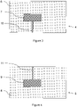
- Figure 1 shows a flexible, rectangle of film 1 in which a thin rectangle of polyvinylidene fluoride (PVDF) 2 is surrounded by an adhesive sheet 3.
- PVDF polyvinylidene fluoride
- the rectangle of film 1 shown in Figure 1 may be the entire film, or it may be part of a larger film, which may contain multiple PVDF rectangles-e.g., a regularly-spaced rectangular grid of such rectangles.
- Figure 2 shows a side view of the film 1, along the line A-A in Figure 1 .
- the rectangle of PVDF 2 and the adhesive sheet 3 have the same thickness as each other, which is also the thickness of the film 1. This thickness may be from 5 to 50 micrometres.
- the film 1 may be fabricated by creating a uniform rectangular sheet of partially-cured epoxy or acrylic adhesive, and then cutting the rectangle out-e.g., using milling, laser cutting, or die cutting-and replacing it with the PVDF 2.
- a flexible upper circuit sheet 4 and a flexible lower circuit sheet 5 are shown above the film 1 and below the film 1, respectively, lying parallel with the film 1. These sheets 4, 5 are shown in a spaced-apart relationship with the film 1, for ease of viewing. However, in reality, these circuit sheets 4, 5 will be placed in contact with the film 1 prior to lamination, and will be bonded to the film 1 after lamination.
- the upper circuit sheet 4 has a polymer layer 6, which may be polyimide (PI) or polyethyleneimine (PEI).
- a patterned metal layer has been deposited or etched on the underside of the polymer layer. This metal layer includes a rectangular electrode 7, which is aligned with (although smaller than) the PVDF rectangle 2 in the film 1.
- the lower circuit sheet 5 has a polymer layer 8, which may be PI or PEI.
- a patterned metal layer has been deposited or etched on the upper face of the polymer layer. This metal layer includes a rectangular electrode 9, which is aligned with the metal rectangle 7 of the upper circuit sheet 4.
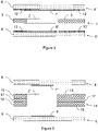
- Figure 3 shows the underside of the upper circuit sheet 4.
- the patterned metal layer may provide other circuit features such as a wire 10 for connecting the electrode 7 to an electrical circuit which may include components that are located off the film 1.
- Figure 4 shows the top side of the lower circuit sheet 5. This may similarly include other circuit features such as a wire 11 for connecting the electrode 9 to the same electrical circuit as the electrode 7 on the upper circuit sheet 4.
- the film 1 is sandwiched between the upper circuit sheet 4 and the lower circuit sheet 5, and heat and pressure are applied-e.g., by a heated press or roller.
- heat and pressure are applied-e.g., by a heated press or roller.
- This causes the polymer layers 6, 8 of the circuit sheets 4, 5 to stick to the upper and lower faces, respectively, of the adhesive sheet 3 of the film 1, everywhere except adjacent the rectangle of PVDF 2.
- the electrodes 7, 9 will contact the rectangle of PVDF 2 and will make physical and electrical contact by a combination of mechanisms.
- the exposed surfaces of the electrodes 7, 9 and/or the PVDF rectangle 2 may be treated with a plasma and/or a chemical primer, such as a silane, to improve the bonding.
- a plasma and/or a chemical primer such as a silane
- This surface treatment preferably influences only a few molecular layers around the electrode-PVDF interface, to minimize the electric field reduction in the PVDF 2.
- the electrodes 7, 9 are used to apply an electrical field across the rectangle of PVDF 2 in order to polarise the PVDF 2 so as to cause it to become piezoelectric.
- the laminated device may be used as, or incorporated into, a microphone, loudspeaker, actuator, or other component or circuit, as required.
- a different type of piezoelectric material may be used in the film 1, so long as it can be adapted to the temperature and pressure required for the bonding procedure, and embedding between the flexible circuits 4, 5.
- Examples of applicable piezoelectric material are P(VDF-TrFE), other copolymers of PVDF, and composites of ceramic powder mixed with one or more polymers.
- the piezoelectric material could also have different initial forms when it is inserted in a lamination press-for example, being a fluid or gel mixed with a solvent. It might instead be in the solid phase-e.g., in the form of a pellet, a powder or a film.
- the piezoelectric material should either be in a melted phase or near melting at least during a part of the lamination cycle, where it can deform toward the flexible circuits 4, 5 and electrodes 7, 9 to provide a sufficient strong bonding as well as uniformity to the facing materials.
- Figure 5 shows an embodiment of the present invention in which the same film 1 is sandwiched between alternative circuit sheets 4', 5'.
- the upper circuit sheet 4' is the same as the upper circuit sheet 4 of Figure 1 except that air gaps in the patterned metal layer, including the rectangular electrode 7', have been filled in with a filling material 12 to provide a planar lower face to the upper circuit sheet 4'. This can improve the bonding to the upper face of the film 1.
- the lower upper circuit sheet 5' is the same as the lower circuit sheet 5 of Figure 1 except that air gaps in the patterned metal layer, including the rectangular electrode 9', have been filled in with a filling material 13 to provide a planar upper face to the lower circuit sheet 5'.
- Figure 6 shows a variant in which an alternative film 14 structure is sandwiched between the upper and lower circuit sheets 4, 5.
- This variant is particularly suitable where a thicker piezoelectric region is desired-e.g., greater than 50 micrometres thick.
- a rectangle of PVDF 2" is surrounded by a three-layered structure comprising an upper adhesive sheet 15, a lower adhesive sheet 16, and-sandwiched between these-a stiffening sheet 17 made of a suitable flexible polymer.
- the film 14 may be formed by laminating complete rectangles of two adhesive sheets with a stiffening sheet, and then cutting out a rectangular hole, to be filled with PVDF 2".
- the variant has additional stiffness, which may simplify handling of the film 14.
Landscapes
- Engineering & Computer Science (AREA)
- Manufacturing & Machinery (AREA)
- Chemical & Material Sciences (AREA)
- Physics & Mathematics (AREA)
- Signal Processing (AREA)
- Acoustics & Sound (AREA)
- Spectroscopy & Molecular Physics (AREA)
- Polymers & Plastics (AREA)
- Organic Chemistry (AREA)
- Health & Medical Sciences (AREA)
- Medicinal Chemistry (AREA)
- Chemical Kinetics & Catalysis (AREA)
- Ceramic Engineering (AREA)
- Composite Materials (AREA)
- Materials Engineering (AREA)
- Piezo-Electric Transducers For Audible Bands (AREA)
- Transducers For Ultrasonic Waves (AREA)
- Laminated Bodies (AREA)
Applications Claiming Priority (2)
| Application Number | Priority Date | Filing Date | Title |
|---|---|---|---|
| GBGB1617171.2A GB201617171D0 (en) | 2016-10-10 | 2016-10-10 | Piezoelectric films |
| PCT/GB2017/053040 WO2018069680A1 (en) | 2016-10-10 | 2017-10-06 | Film with piezoelectric polymer region |
Publications (2)
| Publication Number | Publication Date |
|---|---|
| EP3523833A1 EP3523833A1 (en) | 2019-08-14 |
| EP3523833B1 true EP3523833B1 (en) | 2022-11-16 |
Family
ID=57610592
Family Applications (1)
| Application Number | Title | Priority Date | Filing Date |
|---|---|---|---|
| EP17794039.2A Active EP3523833B1 (en) | 2016-10-10 | 2017-10-06 | Laminated device comprising a film with piezoelectric polymer region |
Country Status (6)
| Country | Link |
|---|---|
| US (2) | US10797222B2 (enExample) |
| EP (1) | EP3523833B1 (enExample) |
| JP (1) | JP7132928B2 (enExample) |
| CA (1) | CA3039437A1 (enExample) |
| GB (1) | GB201617171D0 (enExample) |
| WO (1) | WO2018069680A1 (enExample) |
Families Citing this family (14)
| Publication number | Priority date | Publication date | Assignee | Title |
|---|---|---|---|---|
| GB201617171D0 (en) | 2016-10-10 | 2016-11-23 | Universitetet I Troms� - Norges Arktiske Universitet | Piezoelectric films |
| EP3595515A4 (en) | 2017-03-14 | 2020-12-30 | University of Connecticut | BIODEGRADABLE PRESSURE SENSOR |
| US11678989B2 (en) * | 2019-03-01 | 2023-06-20 | University Of Connecticut | Biodegradable piezoelectric nanofiber scaffold for bone or tissue regeneration |
| US11826495B2 (en) | 2019-03-01 | 2023-11-28 | University Of Connecticut | Biodegradable piezoelectric ultrasonic transducer system |
| WO2021052951A1 (en) | 2019-09-16 | 2021-03-25 | Apollo Tyres Global R&D B.V. | Method for chemically adhering a diene rubber to a piezoelectric polymer |
| US11745001B2 (en) | 2020-03-10 | 2023-09-05 | University Of Connecticut | Therapeutic bandage |
| US12491290B2 (en) | 2020-06-08 | 2025-12-09 | University Of Connecticut | Biodegradable piezoelectric composite materials |
| CN113432763B (zh) * | 2021-06-17 | 2023-07-21 | 中北大学 | 夹芯式pvdf压力计真空环境压制装置及方法 |
| CN113432772B (zh) * | 2021-06-17 | 2023-09-08 | 中北大学 | 物体表面冲击波测量高灵敏薄膜传感器及制作方法 |
| CN113346005B (zh) * | 2021-06-17 | 2024-07-02 | 太原工业学院 | 夹芯式薄膜传感器真空环境压合装置及方法 |
| CN113432773B (zh) * | 2021-06-17 | 2023-10-27 | 中北大学 | 适用于柔性物体表面冲击波压力测量传感器及制作方法 |
| KR102675469B1 (ko) * | 2021-09-29 | 2024-06-17 | 한국기술교육대학교 산학협력단 | 압전 필름 스피커 및 그 제조방법 |
| US12531330B1 (en) | 2024-02-05 | 2026-01-20 | Rockwell Collins, Inc. | Oscillator integrated piezoelectric radiator |
| US12431614B1 (en) | 2024-02-05 | 2025-09-30 | Rockwell Collins, Inc. | Frequency tunable piezoelectric VLF antenna |
Citations (1)
| Publication number | Priority date | Publication date | Assignee | Title |
|---|---|---|---|---|
| EP2919249A1 (en) * | 2012-11-08 | 2015-09-16 | Ajinomoto Co., Inc. | Membrane switch and object employing same |
Family Cites Families (29)
| Publication number | Priority date | Publication date | Assignee | Title |
|---|---|---|---|---|
| AT375466B (de) | 1977-07-27 | 1984-08-10 | List Hans | Messwertaufnehmer mit einem piezoelektrischen messelement |
| AU544447B2 (en) | 1980-02-07 | 1985-05-30 | Toray Industries, Inc. | Vinylidene fluoride and ethylene trifluoride copolymer |
| JPS57126125A (en) | 1981-01-29 | 1982-08-05 | Tokyo Shibaura Electric Co | Piezoelectric or pyroelectric element |
| US5089739A (en) | 1990-03-19 | 1992-02-18 | Brother Kogyo Kabushiki Kaisha | Laminate type piezoelectric actuator element |
| US5288551A (en) | 1991-08-09 | 1994-02-22 | Kureha Kagaku Kogyo Kabushiki Kaisha | Flexible piezoelectric device |
| US6420819B1 (en) | 1994-01-27 | 2002-07-16 | Active Control Experts, Inc. | Packaged strain actuator |
| US5702629A (en) | 1996-03-21 | 1997-12-30 | Alliedsignal Inc. | Piezeoelectric ceramic-polymer composites |
| JP3575373B2 (ja) * | 1999-04-19 | 2004-10-13 | 株式会社村田製作所 | 外力検知センサの製造方法 |
| JP2001250993A (ja) | 2000-03-03 | 2001-09-14 | Matsushita Electric Ind Co Ltd | 可撓性圧電素子およびその製造方法 |
| US20040263483A1 (en) * | 2003-06-24 | 2004-12-30 | Aufderheide Brian E | Sensing device |
| JP5044196B2 (ja) | 2006-11-13 | 2012-10-10 | アイシン精機株式会社 | 圧電センサ及びその製造方法 |
| CN101714608B (zh) | 2009-12-01 | 2011-05-25 | 同济大学 | 压电聚合物薄膜传感器的封装方法 |
| WO2011121882A1 (ja) | 2010-03-31 | 2011-10-06 | コニカミノルタエムジー株式会社 | 積層型圧電体および積層型圧電体の製造方法ならびに前記積層型圧電体を用いた超音波トランスデューサおよび超音波診断装置 |
| US8585187B2 (en) | 2011-04-29 | 2013-11-19 | Xerox Corporation | High density electrical interconnect for printing devices using flex circuits and dielectric underfill |
| DE102011107421A1 (de) * | 2011-07-07 | 2013-01-10 | Leonhard Kurz Stiftung & Co. Kg | Mehrschichtiger Folienkörper |
| KR20140073201A (ko) | 2012-12-06 | 2014-06-16 | 한국전자통신연구원 | 압전 에너지 하베스팅 장치 및 그 제조 방법 |
| JP6415451B2 (ja) * | 2012-12-28 | 2018-10-31 | ダウ シリコーンズ コーポレーション | トランスデューサー用硬化性オルガノシロキサン組成物及び硬化性シリコーン組成物のトランスデューサーへの使用 |
| JP5686443B2 (ja) | 2013-01-10 | 2015-03-18 | 日本写真印刷株式会社 | 接着層付きフィルム状感圧センサとこれを用いたタッチパッド、タッチ入力機能付き保護パネル及び電子機器 |
| JP6041978B2 (ja) | 2013-03-21 | 2016-12-14 | 株式会社村田製作所 | 変位センサ、押込量検出センサ、およびタッチ式入力装置 |
| WO2015077200A1 (en) | 2013-11-21 | 2015-05-28 | 3M Innovative Properties Company | Multi-layer piezoelectric polymer film devices and methods |
| EP2894631B1 (en) * | 2013-12-20 | 2018-08-22 | Samsung Medison Co., Ltd. | Ultrasonic diagnostic apparatus and manufacturing method thereof |
| WO2015129061A1 (ja) | 2014-02-27 | 2015-09-03 | 京セラ株式会社 | 圧電アクチュエータおよびこれを備えた圧電振動装置、携帯端末、音響発生器、音響発生装置、電子機器 |
| CN106489119B (zh) | 2014-07-02 | 2020-02-18 | 株式会社村田制作所 | 触摸面板 |
| WO2016027667A1 (ja) | 2014-08-21 | 2016-02-25 | 株式会社村田製作所 | 振動体及び触覚提示キーボード |
| KR101612456B1 (ko) * | 2014-09-12 | 2016-04-14 | 한국세라믹기술원 | 압전 파이버 컴포지트 구조체 및 이를 이용한 압전 스피커 |
| GB201617171D0 (en) | 2016-10-10 | 2016-11-23 | Universitetet I Troms� - Norges Arktiske Universitet | Piezoelectric films |
| KR102640240B1 (ko) * | 2016-10-31 | 2024-02-22 | 엘지디스플레이 주식회사 | 접촉 감응 소자 및 이를 포함하는 표시 장치 |
| CN109937488A (zh) * | 2016-11-14 | 2019-06-25 | 皇家飞利浦有限公司 | 用于电活性致动器的刚度控制 |
| US20190354222A1 (en) * | 2017-01-06 | 2019-11-21 | Sabic Global Technologies B.V. | Triboelectric sensor with haptic feedback |
-
2016
- 2016-10-10 GB GBGB1617171.2A patent/GB201617171D0/en not_active Ceased
-
2017
- 2017-10-06 WO PCT/GB2017/053040 patent/WO2018069680A1/en not_active Ceased
- 2017-10-06 JP JP2019540713A patent/JP7132928B2/ja active Active
- 2017-10-06 EP EP17794039.2A patent/EP3523833B1/en active Active
- 2017-10-06 US US16/340,614 patent/US10797222B2/en not_active Expired - Fee Related
- 2017-10-06 CA CA3039437A patent/CA3039437A1/en active Pending
-
2020
- 2020-02-28 US US16/805,301 patent/US11450800B2/en active Active
Patent Citations (1)
| Publication number | Priority date | Publication date | Assignee | Title |
|---|---|---|---|---|
| EP2919249A1 (en) * | 2012-11-08 | 2015-09-16 | Ajinomoto Co., Inc. | Membrane switch and object employing same |
Also Published As
| Publication number | Publication date |
|---|---|
| US20200373477A1 (en) | 2020-11-26 |
| JP2019530988A (ja) | 2019-10-24 |
| CA3039437A1 (en) | 2018-04-19 |
| JP7132928B2 (ja) | 2022-09-07 |
| US20190319181A1 (en) | 2019-10-17 |
| WO2018069680A1 (en) | 2018-04-19 |
| US10797222B2 (en) | 2020-10-06 |
| EP3523833A1 (en) | 2019-08-14 |
| US11450800B2 (en) | 2022-09-20 |
| GB201617171D0 (en) | 2016-11-23 |
Similar Documents
| Publication | Publication Date | Title |
|---|---|---|
| US11450800B2 (en) | Film with piezoelectric polymer region | |
| JP7609950B2 (ja) | 圧電素子 | |
| US9812634B2 (en) | Method of making thick film transducer arrays | |
| KR101603957B1 (ko) | 압전 액추에이터, 압전 진동 장치 및 휴대 단말 | |
| GB2229855A (en) | Laminated piezoelectric structures and process of forming the same | |
| WO2014098077A1 (ja) | 圧電アクチュエータ、圧電振動装置および携帯端末 | |
| TW200934271A (en) | Sound-generating device | |
| WO2015129061A1 (ja) | 圧電アクチュエータおよびこれを備えた圧電振動装置、携帯端末、音響発生器、音響発生装置、電子機器 | |
| JP7259075B2 (ja) | 圧電素子 | |
| TW202205705A (zh) | 壓電元件 | |
| JP6450416B2 (ja) | 超音波トランスデューサ及びその製造方法 | |
| WO2013171915A1 (ja) | 圧電アクチュエータ、圧電振動装置および携帯端末 | |
| CN116783902A (zh) | 压电薄膜 | |
| TW202119661A (zh) | 壓電元件 | |
| WO2014050240A1 (ja) | 圧電アクチュエータ、圧電振動装置および携帯端末 | |
| KR102298213B1 (ko) | 다층 구조의 멤브레인을 가진 초음파 트랜스듀서 및 이의 제작 방법 | |
| JP2004364334A (ja) | 圧電音響変換器 | |
| WO2013171918A1 (ja) | 圧電アクチュエータ、圧電振動装置および携帯端末 | |
| TW202236704A (zh) | 壓電薄膜 | |
| EP3545565B1 (en) | 2d ultrasound transducer array methods of making the same | |
| JP2003038486A (ja) | 超音波探触子 |
Legal Events
| Date | Code | Title | Description |
|---|---|---|---|
| STAA | Information on the status of an ep patent application or granted ep patent |
Free format text: STATUS: UNKNOWN |
|
| STAA | Information on the status of an ep patent application or granted ep patent |
Free format text: STATUS: THE INTERNATIONAL PUBLICATION HAS BEEN MADE |
|
| PUAI | Public reference made under article 153(3) epc to a published international application that has entered the european phase |
Free format text: ORIGINAL CODE: 0009012 |
|
| STAA | Information on the status of an ep patent application or granted ep patent |
Free format text: STATUS: REQUEST FOR EXAMINATION WAS MADE |
|
| 17P | Request for examination filed |
Effective date: 20190415 |
|
| AK | Designated contracting states |
Kind code of ref document: A1 Designated state(s): AL AT BE BG CH CY CZ DE DK EE ES FI FR GB GR HR HU IE IS IT LI LT LU LV MC MK MT NL NO PL PT RO RS SE SI SK SM TR |
|
| AX | Request for extension of the european patent |
Extension state: BA ME |
|
| RIN1 | Information on inventor provided before grant (corrected) |
Inventor name: WAGLE, SANAT Inventor name: MELANDSOE, FRANK Inventor name: HABIB, ANOWARUL |
|
| DAV | Request for validation of the european patent (deleted) | ||
| DAX | Request for extension of the european patent (deleted) | ||
| STAA | Information on the status of an ep patent application or granted ep patent |
Free format text: STATUS: EXAMINATION IS IN PROGRESS |
|
| 17Q | First examination report despatched |
Effective date: 20200707 |
|
| GRAP | Despatch of communication of intention to grant a patent |
Free format text: ORIGINAL CODE: EPIDOSNIGR1 |
|
| STAA | Information on the status of an ep patent application or granted ep patent |
Free format text: STATUS: GRANT OF PATENT IS INTENDED |
|
| INTG | Intention to grant announced |
Effective date: 20210624 |
|
| GRAJ | Information related to disapproval of communication of intention to grant by the applicant or resumption of examination proceedings by the epo deleted |
Free format text: ORIGINAL CODE: EPIDOSDIGR1 |
|
| STAA | Information on the status of an ep patent application or granted ep patent |
Free format text: STATUS: EXAMINATION IS IN PROGRESS |
|
| GRAP | Despatch of communication of intention to grant a patent |
Free format text: ORIGINAL CODE: EPIDOSNIGR1 |
|
| STAA | Information on the status of an ep patent application or granted ep patent |
Free format text: STATUS: GRANT OF PATENT IS INTENDED |
|
| INTC | Intention to grant announced (deleted) | ||
| INTG | Intention to grant announced |
Effective date: 20211130 |
|
| GRAS | Grant fee paid |
Free format text: ORIGINAL CODE: EPIDOSNIGR3 |
|
| GRAL | Information related to payment of fee for publishing/printing deleted |
Free format text: ORIGINAL CODE: EPIDOSDIGR3 |
|
| GRAS | Grant fee paid |
Free format text: ORIGINAL CODE: EPIDOSNIGR3 |
|
| GRAA | (expected) grant |
Free format text: ORIGINAL CODE: 0009210 |
|
| STAA | Information on the status of an ep patent application or granted ep patent |
Free format text: STATUS: THE PATENT HAS BEEN GRANTED |
|
| AK | Designated contracting states |
Kind code of ref document: B1 Designated state(s): AL AT BE BG CH CY CZ DE DK EE ES FI FR GB GR HR HU IE IS IT LI LT LU LV MC MK MT NL NO PL PT RO RS SE SI SK SM TR |
|
| REG | Reference to a national code |
Ref country code: GB Ref legal event code: FG4D |
|
| REG | Reference to a national code |
Ref country code: DE Ref legal event code: R079 Ref document number: 602017063780 Country of ref document: DE Free format text: PREVIOUS MAIN CLASS: H01L0041053000 Ipc: H10N0030880000 |
|
| REG | Reference to a national code |
Ref country code: CH Ref legal event code: EP |
|
| REG | Reference to a national code |
Ref country code: IE Ref legal event code: FG4D |
|
| REG | Reference to a national code |
Ref country code: DE Ref legal event code: R096 Ref document number: 602017063780 Country of ref document: DE |
|
| REG | Reference to a national code |
Ref country code: AT Ref legal event code: REF Ref document number: 1532306 Country of ref document: AT Kind code of ref document: T Effective date: 20221215 |
|
| REG | Reference to a national code |
Ref country code: LT Ref legal event code: MG9D |
|
| REG | Reference to a national code |
Ref country code: NL Ref legal event code: MP Effective date: 20221116 |
|
| REG | Reference to a national code |
Ref country code: AT Ref legal event code: MK05 Ref document number: 1532306 Country of ref document: AT Kind code of ref document: T Effective date: 20221116 |
|
| PG25 | Lapsed in a contracting state [announced via postgrant information from national office to epo] |
Ref country code: NO Free format text: LAPSE BECAUSE OF FAILURE TO SUBMIT A TRANSLATION OF THE DESCRIPTION OR TO PAY THE FEE WITHIN THE PRESCRIBED TIME-LIMIT Effective date: 20230216 Ref country code: LT Free format text: LAPSE BECAUSE OF FAILURE TO SUBMIT A TRANSLATION OF THE DESCRIPTION OR TO PAY THE FEE WITHIN THE PRESCRIBED TIME-LIMIT Effective date: 20221116 Ref country code: FI Free format text: LAPSE BECAUSE OF FAILURE TO SUBMIT A TRANSLATION OF THE DESCRIPTION OR TO PAY THE FEE WITHIN THE PRESCRIBED TIME-LIMIT Effective date: 20221116 Ref country code: ES Free format text: LAPSE BECAUSE OF FAILURE TO SUBMIT A TRANSLATION OF THE DESCRIPTION OR TO PAY THE FEE WITHIN THE PRESCRIBED TIME-LIMIT Effective date: 20221116 Ref country code: AT Free format text: LAPSE BECAUSE OF FAILURE TO SUBMIT A TRANSLATION OF THE DESCRIPTION OR TO PAY THE FEE WITHIN THE PRESCRIBED TIME-LIMIT Effective date: 20221116 Ref country code: SE Free format text: LAPSE BECAUSE OF FAILURE TO SUBMIT A TRANSLATION OF THE DESCRIPTION OR TO PAY THE FEE WITHIN THE PRESCRIBED TIME-LIMIT Effective date: 20221116 Ref country code: PT Free format text: LAPSE BECAUSE OF FAILURE TO SUBMIT A TRANSLATION OF THE DESCRIPTION OR TO PAY THE FEE WITHIN THE PRESCRIBED TIME-LIMIT Effective date: 20230316 |
|
| PG25 | Lapsed in a contracting state [announced via postgrant information from national office to epo] |
Ref country code: RS Free format text: LAPSE BECAUSE OF FAILURE TO SUBMIT A TRANSLATION OF THE DESCRIPTION OR TO PAY THE FEE WITHIN THE PRESCRIBED TIME-LIMIT Effective date: 20221116 Ref country code: PL Free format text: LAPSE BECAUSE OF FAILURE TO SUBMIT A TRANSLATION OF THE DESCRIPTION OR TO PAY THE FEE WITHIN THE PRESCRIBED TIME-LIMIT Effective date: 20221116 Ref country code: LV Free format text: LAPSE BECAUSE OF FAILURE TO SUBMIT A TRANSLATION OF THE DESCRIPTION OR TO PAY THE FEE WITHIN THE PRESCRIBED TIME-LIMIT Effective date: 20221116 Ref country code: IS Free format text: LAPSE BECAUSE OF FAILURE TO SUBMIT A TRANSLATION OF THE DESCRIPTION OR TO PAY THE FEE WITHIN THE PRESCRIBED TIME-LIMIT Effective date: 20230316 Ref country code: HR Free format text: LAPSE BECAUSE OF FAILURE TO SUBMIT A TRANSLATION OF THE DESCRIPTION OR TO PAY THE FEE WITHIN THE PRESCRIBED TIME-LIMIT Effective date: 20221116 Ref country code: GR Free format text: LAPSE BECAUSE OF FAILURE TO SUBMIT A TRANSLATION OF THE DESCRIPTION OR TO PAY THE FEE WITHIN THE PRESCRIBED TIME-LIMIT Effective date: 20230217 |
|
| PG25 | Lapsed in a contracting state [announced via postgrant information from national office to epo] |
Ref country code: NL Free format text: LAPSE BECAUSE OF FAILURE TO SUBMIT A TRANSLATION OF THE DESCRIPTION OR TO PAY THE FEE WITHIN THE PRESCRIBED TIME-LIMIT Effective date: 20221116 |
|
| PG25 | Lapsed in a contracting state [announced via postgrant information from national office to epo] |
Ref country code: SM Free format text: LAPSE BECAUSE OF FAILURE TO SUBMIT A TRANSLATION OF THE DESCRIPTION OR TO PAY THE FEE WITHIN THE PRESCRIBED TIME-LIMIT Effective date: 20221116 Ref country code: RO Free format text: LAPSE BECAUSE OF FAILURE TO SUBMIT A TRANSLATION OF THE DESCRIPTION OR TO PAY THE FEE WITHIN THE PRESCRIBED TIME-LIMIT Effective date: 20221116 Ref country code: EE Free format text: LAPSE BECAUSE OF FAILURE TO SUBMIT A TRANSLATION OF THE DESCRIPTION OR TO PAY THE FEE WITHIN THE PRESCRIBED TIME-LIMIT Effective date: 20221116 Ref country code: DK Free format text: LAPSE BECAUSE OF FAILURE TO SUBMIT A TRANSLATION OF THE DESCRIPTION OR TO PAY THE FEE WITHIN THE PRESCRIBED TIME-LIMIT Effective date: 20221116 Ref country code: CZ Free format text: LAPSE BECAUSE OF FAILURE TO SUBMIT A TRANSLATION OF THE DESCRIPTION OR TO PAY THE FEE WITHIN THE PRESCRIBED TIME-LIMIT Effective date: 20221116 |
|
| REG | Reference to a national code |
Ref country code: DE Ref legal event code: R097 Ref document number: 602017063780 Country of ref document: DE |
|
| PG25 | Lapsed in a contracting state [announced via postgrant information from national office to epo] |
Ref country code: SK Free format text: LAPSE BECAUSE OF FAILURE TO SUBMIT A TRANSLATION OF THE DESCRIPTION OR TO PAY THE FEE WITHIN THE PRESCRIBED TIME-LIMIT Effective date: 20221116 Ref country code: AL Free format text: LAPSE BECAUSE OF FAILURE TO SUBMIT A TRANSLATION OF THE DESCRIPTION OR TO PAY THE FEE WITHIN THE PRESCRIBED TIME-LIMIT Effective date: 20221116 |
|
| PLBE | No opposition filed within time limit |
Free format text: ORIGINAL CODE: 0009261 |
|
| STAA | Information on the status of an ep patent application or granted ep patent |
Free format text: STATUS: NO OPPOSITION FILED WITHIN TIME LIMIT |
|
| 26N | No opposition filed |
Effective date: 20230817 |
|
| PG25 | Lapsed in a contracting state [announced via postgrant information from national office to epo] |
Ref country code: SI Free format text: LAPSE BECAUSE OF FAILURE TO SUBMIT A TRANSLATION OF THE DESCRIPTION OR TO PAY THE FEE WITHIN THE PRESCRIBED TIME-LIMIT Effective date: 20221116 |
|
| REG | Reference to a national code |
Ref country code: DE Ref legal event code: R119 Ref document number: 602017063780 Country of ref document: DE |
|
| PG25 | Lapsed in a contracting state [announced via postgrant information from national office to epo] |
Ref country code: IT Free format text: LAPSE BECAUSE OF FAILURE TO SUBMIT A TRANSLATION OF THE DESCRIPTION OR TO PAY THE FEE WITHIN THE PRESCRIBED TIME-LIMIT Effective date: 20221116 Ref country code: MC Free format text: LAPSE BECAUSE OF FAILURE TO SUBMIT A TRANSLATION OF THE DESCRIPTION OR TO PAY THE FEE WITHIN THE PRESCRIBED TIME-LIMIT Effective date: 20221116 |
|
| REG | Reference to a national code |
Ref country code: CH Ref legal event code: PL |
|
| REG | Reference to a national code |
Ref country code: BE Ref legal event code: MM Effective date: 20231031 |
|
| PG25 | Lapsed in a contracting state [announced via postgrant information from national office to epo] |
Ref country code: LU Free format text: LAPSE BECAUSE OF NON-PAYMENT OF DUE FEES Effective date: 20231006 |
|
| GBPC | Gb: european patent ceased through non-payment of renewal fee |
Effective date: 20231006 |
|
| PG25 | Lapsed in a contracting state [announced via postgrant information from national office to epo] |
Ref country code: LU Free format text: LAPSE BECAUSE OF NON-PAYMENT OF DUE FEES Effective date: 20231006 |
|
| PG25 | Lapsed in a contracting state [announced via postgrant information from national office to epo] |
Ref country code: GB Free format text: LAPSE BECAUSE OF NON-PAYMENT OF DUE FEES Effective date: 20231006 |
|
| PG25 | Lapsed in a contracting state [announced via postgrant information from national office to epo] |
Ref country code: CH Free format text: LAPSE BECAUSE OF NON-PAYMENT OF DUE FEES Effective date: 20231031 |
|
| PG25 | Lapsed in a contracting state [announced via postgrant information from national office to epo] |
Ref country code: GB Free format text: LAPSE BECAUSE OF NON-PAYMENT OF DUE FEES Effective date: 20231006 Ref country code: FR Free format text: LAPSE BECAUSE OF NON-PAYMENT OF DUE FEES Effective date: 20231031 Ref country code: DE Free format text: LAPSE BECAUSE OF NON-PAYMENT OF DUE FEES Effective date: 20240501 Ref country code: CH Free format text: LAPSE BECAUSE OF NON-PAYMENT OF DUE FEES Effective date: 20231031 |
|
| PG25 | Lapsed in a contracting state [announced via postgrant information from national office to epo] |
Ref country code: BE Free format text: LAPSE BECAUSE OF NON-PAYMENT OF DUE FEES Effective date: 20231031 |
|
| PG25 | Lapsed in a contracting state [announced via postgrant information from national office to epo] |
Ref country code: IE Free format text: LAPSE BECAUSE OF NON-PAYMENT OF DUE FEES Effective date: 20231006 |
|
| PG25 | Lapsed in a contracting state [announced via postgrant information from national office to epo] |
Ref country code: IE Free format text: LAPSE BECAUSE OF NON-PAYMENT OF DUE FEES Effective date: 20231006 |
|
| PG25 | Lapsed in a contracting state [announced via postgrant information from national office to epo] |
Ref country code: BG Free format text: LAPSE BECAUSE OF FAILURE TO SUBMIT A TRANSLATION OF THE DESCRIPTION OR TO PAY THE FEE WITHIN THE PRESCRIBED TIME-LIMIT Effective date: 20221116 |
|
| PG25 | Lapsed in a contracting state [announced via postgrant information from national office to epo] |
Ref country code: BG Free format text: LAPSE BECAUSE OF FAILURE TO SUBMIT A TRANSLATION OF THE DESCRIPTION OR TO PAY THE FEE WITHIN THE PRESCRIBED TIME-LIMIT Effective date: 20221116 |
|
| PG25 | Lapsed in a contracting state [announced via postgrant information from national office to epo] |
Ref country code: CY Free format text: LAPSE BECAUSE OF FAILURE TO SUBMIT A TRANSLATION OF THE DESCRIPTION OR TO PAY THE FEE WITHIN THE PRESCRIBED TIME-LIMIT; INVALID AB INITIO Effective date: 20171006 |
|
| PG25 | Lapsed in a contracting state [announced via postgrant information from national office to epo] |
Ref country code: HU Free format text: LAPSE BECAUSE OF FAILURE TO SUBMIT A TRANSLATION OF THE DESCRIPTION OR TO PAY THE FEE WITHIN THE PRESCRIBED TIME-LIMIT; INVALID AB INITIO Effective date: 20171006 |
|
| PG25 | Lapsed in a contracting state [announced via postgrant information from national office to epo] |
Ref country code: TR Free format text: LAPSE BECAUSE OF FAILURE TO SUBMIT A TRANSLATION OF THE DESCRIPTION OR TO PAY THE FEE WITHIN THE PRESCRIBED TIME-LIMIT Effective date: 20221116 |